limits of fr-4 in high-speed designs -...
TRANSCRIPT

Successful Design of OC-48/2.5Gbps InterconnectsSlide 1
High Performance Engineering & Design
http://www.nesa.com
Limits of FR-4 inLimits of FR-4 inHigh-Speed DesignsHigh-Speed Designs
Dr. Edward Sayre, Mr. Michael Baxter, Dr. Jinhua ChenNESA
Tel: 978 897-8787 v Fax: 978 897-5359www.nesa.com v [email protected]
Successful Design of OC-48/2.5Gbps InterconnectsSlide 2
High Performance Engineering & Design
http://www.nesa.com
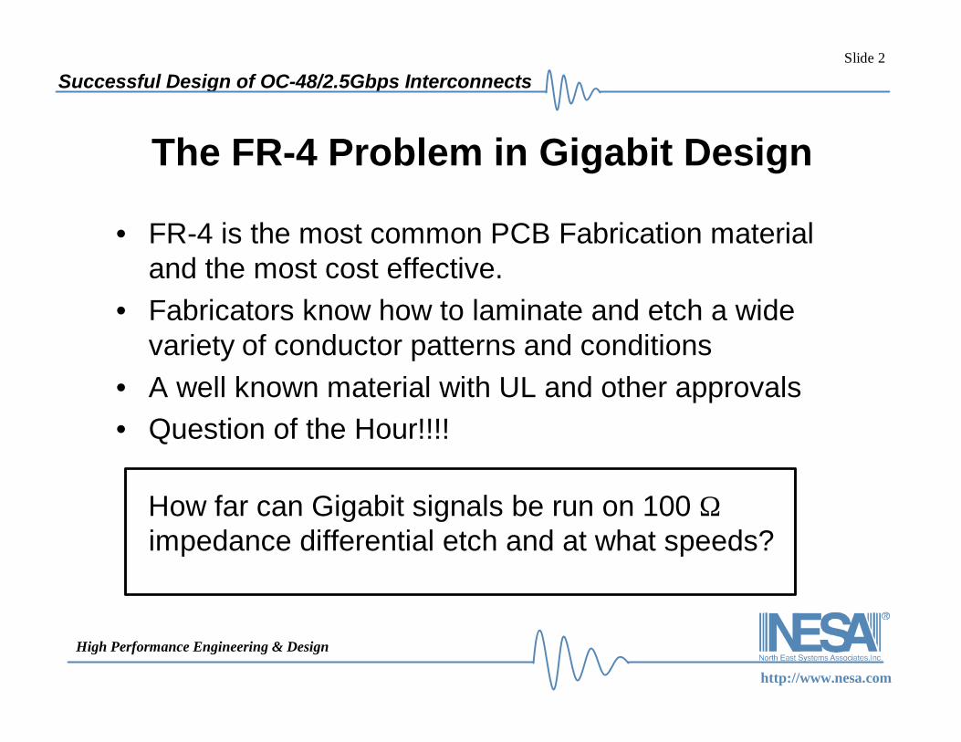
The FR-4 Problem in Gigabit Design
• FR-4 is the most common PCB Fabrication materialand the most cost effective.
• Fabricators know how to laminate and etch a widevariety of conductor patterns and conditions
• A well known material with UL and other approvals• Question of the Hour!!!!
How far can Gigabit signals be run on 100 Ωimpedance differential etch and at what speeds?

Successful Design of OC-48/2.5Gbps InterconnectsSlide 3
High Performance Engineering & Design
http://www.nesa.com
Total RF Transmission Line Loss
++=0
0**35.4)(Z
fRRZfGdB
LengthUnitPernAttenuatio sdc
d
Where: Gd = shunt dielectric conductance [Ω Hz]-1 Rs = skin effect series loss [Ω (Hz)-1/2]

Successful Design of OC-48/2.5Gbps InterconnectsSlide 4
High Performance Engineering & Design
http://www.nesa.com
Frequency Where Skin Effect LossesEqual Dielectric Losses
2
20
1
•≡
ZGRf
d
se
Where: Rs = Skin Effect Resistance [Ω(Hz)-1/2]Gd = Dielectric Shunt Conductance [Ω Hz]-1Zo = Transmission Line Impedance [Ω ]
Successful Design of OC-48/2.5Gbps InterconnectsSlide 5
High Performance Engineering & Design
http://www.nesa.com
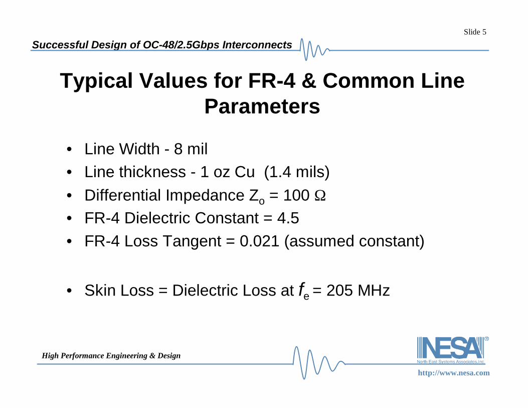
• Line Width - 8 mil• Line thickness - 1 oz Cu (1.4 mils)• Differential Impedance Zo = 100 Ω• FR-4 Dielectric Constant = 4.5• FR-4 Loss Tangent = 0.021 (assumed constant)
• Skin Loss = Dielectric Loss at fe = 205 MHz
Typical Values for FR-4 & Common LineParameters

Successful Design of OC-48/2.5Gbps InterconnectsSlide 6
High Performance Engineering & Design
http://www.nesa.com
RF Total Loss vs. Normalized FrequencyTotal Loss (% )
0.0%
10.0%20.0%
30.0%
40.0%
50.0%60.0%
70.0%
80.0%
0 1 2 3 4 5 6 7 8 9 10
Normalized Frequency (f /f e)
Perc
enta
ge L
oss

Successful Design of OC-48/2.5Gbps InterconnectsSlide 7
High Performance Engineering & Design
http://www.nesa.com
100 Ω Differential PCB percentage peak to peak loss as the function of
data rate, PCB lengths from 10” to 50” with 8 mil line width
0.00
10.00
20.00
30.00
40.00
50.00
60.00
70.00
80.00
0.0 0.5 1.0 1.5 2.0 2.5 3.0 3.5 4.0 4.5 5.0 5.5
Data Rate (Gbps)
PCB
Pea
k to
Pea
k Lo
ss (%
)
10"
20"
30"
40"50"

Successful Design of OC-48/2.5Gbps InterconnectsSlide 8
High Performance Engineering & Design
http://www.nesa.com
0.00
10.00
20.00
30.00
40.00
50.00
60.00
70.00
80.00
0.0 10.0 20.0 30.0 40.0 50.0 60.0
PCB Length (inch)
PCB
Pea
k to
Pea
k Lo
ss (%
)
622 Mbps
1.25 Gbps1.6 Gbps
2.5 Gbps
5 Gbps
100 Ω Differential PCB percentage peak to peak loss as the function of
PCB length with 8 mil line width

Successful Design of OC-48/2.5Gbps InterconnectsSlide 9
High Performance Engineering & Design
http://www.nesa.com
0.00
10.00
20.00
30.00
40.00
50.00
60.00
70.00
80.00
0.00 0.50 1.00 1.50 2.00 2.50 3.00 3.50 4.00 4.50 5.00 5.50
Data Rate (Gbps)
PCB
Pea
k to
Pea
k Lo
ss (%
)
10"
20"
30"
40"
50"
100 Ω Differential PCB percentage peak to peak loss as the function of
data rate, PCB lengths from 10” to 50” with 6 mil line width

Successful Design of OC-48/2.5Gbps InterconnectsSlide 10
High Performance Engineering & Design
http://www.nesa.com
0.00
10.00
20.00
30.00
40.00
50.00
60.00
70.00
80.00
0.0 10.0 20.0 30.0 40.0 50.0 60.0
PCB Length (inch)
PCB
Pea
k to
Pea
k Lo
ss (%
)
622 Mbps
1.25 Gbps
1.6 Gbps
2.5 Gbps
5 Gbps
100 Ω Differential PCB percentage peak to peak loss as the function of
PCB length with 6 mil line width

Successful Design of OC-48/2.5Gbps InterconnectsSlide 11
High Performance Engineering & Design
http://www.nesa.com
0.0
10.0
20.0
30.0
40.0
50.0
60.0
70.0
80.0
0.00 0.50 1.00 1.50 2.00 2.50 3.00 3.50 4.00 4.50 5.00 5.50
Data Rate (Gbps)
PCB
Peak
to P
eak
Loss
(%)
10"
20"
30"
40"
50"
100 Ω Differential PCB percentage peak to peak loss as the function of
data rate, PCB lengths from 10” to 50” with 4 mil line width

Successful Design of OC-48/2.5Gbps InterconnectsSlide 12
High Performance Engineering & Design
http://www.nesa.com
100 Ω Differential PCB percentage peak to peak loss as the function of
PCB length with 4 mil line width
0.0
10.0
20.0
30.0
40.0
50.0
60.0
70.0
80.0
0.00 10.00 20.00 30.00 40.00 50.00 60.00
PCB Length (inch)
PCB
Pea
k to
Pea
k Lo
ss (%
)
622 Mbps
1.25 Gbps1.6 Gbps
2.5 Gbps
5 Gbps

Successful Design of OC-48/2.5Gbps InterconnectsSlide 13
High Performance Engineering & Design
http://www.nesa.com
0.00
10.00
20.00
30.00
40.00
50.00
60.00
0.00 0.50 1.00 1.50 2.00 2.50 3.00 3.50 4.00 4.50 5.00 5.50
Data Rate (Gbps)
PCB
Pea
k to
Pea
k Lo
ss (%
)
8 mils
6 mils4 mils
100 Ω Differential PCBpercentage peak to peak loss as the function of data rate
30" traces with 4, 6 and 8 mil line width

Successful Design of OC-48/2.5Gbps InterconnectsSlide 14
High Performance Engineering & Design
http://www.nesa.com
-0.8
-0.6
-0.4
-0.2
0
0.2
0.4
0.6
0.8
0 0.1 0.2 0.3 0.4
Time (ns)
Vo
ltag
e (
V)
Simulated 2.5 Gbps Eye Patternskin effect + dielectric loss (FR-4 loss tangent 0.021) for 40” trace

Successful Design of OC-48/2.5Gbps InterconnectsSlide 15
High Performance Engineering & Design
http://www.nesa.com
-0.8
-0.6
-0.4
-0.2
0
0.2
0.4
0.6
0.8
0 0.1 0.2 0.3 0.4
Time (ns)
Vo
ltag
e (
V)
Simulated 2.5 Gbps Eye Pattern skin effect + dielectric loss for 40” trace with two backplane connectors

Successful Design of OC-48/2.5Gbps InterconnectsSlide 16
High Performance Engineering & Design
http://www.nesa.com
LONG CONTROL PAIR EYE DIAGRAM, 2.5GBPS
Measured 2.5 Gbps Eye Pattern skin effect + dielectric loss for 40” trace with two backplane connectors

Successful Design of OC-48/2.5Gbps InterconnectsSlide 17
High Performance Engineering & Design
http://www.nesa.com
Differential 1.25 Gbps Eye Pattern23” trace including two backplane connectors

Successful Design of OC-48/2.5Gbps InterconnectsSlide 18
High Performance Engineering & Design
http://www.nesa.com
SMA Connector
Skin Effect Region
Highly ResistiveLossy Etch
Poor Fabrication ResultsDifferential TDR vs. Risetime

Successful Design of OC-48/2.5Gbps InterconnectsSlide 19
High Performance Engineering & Design
http://www.nesa.com
1.25 Gbps Eye Patternproperly etched differential pair

Successful Design of OC-48/2.5Gbps InterconnectsSlide 20
High Performance Engineering & Design
http://www.nesa.com
1.25 Gbps Eye Patternover-etched differential pair

Successful Design of OC-48/2.5Gbps InterconnectsSlide 21
High Performance Engineering & Design
http://www.nesa.com
FR-4 PCB Limits - Summary• Eye Diagram Response
– Deterministic Jitter and Risetime Losses are well known and due to dielectricand conductor skin effect losses.
– Eye diagram mask violations in amplitude or bit time jitter lead to unacceptableBit Error Rates
• Fabrication Quality of PCB traces strongly affects eye response.– 100 Ω impedance line losses not strongly affected by line size.
• Semiconductor pulse fidelity and receiver determining factors– Receiver threshold region < (15 - 20%) of swing OK– Risetimes <(15 - 20)% of bit width reduces mask violations
• FR-4 max. line length depends on devices, bit rate, reflections and losses– As a practical matter, jitter more forcefully impacted by bandwidth limits due to
losses– Connector reflections shorten maximum length.
• Maximum usable clock rate Fclk ~ (7 - 10) * fe at reasonable PCB lengths of0.5 meter to 1.25 meter.