led driver series for lighting step-down type with 1.5a...
TRANSCRIPT
1/11 www.rohm.com 2009.07 - Rev.A
© 2009 ROHM Co., Ltd. All rights reserved.
LED Driver series for lighting Step-down type with 1.5A output BD9207FPS
Description
BD9207FPS is a LED driver with built-in step-down switching regulator and incorporates the built-in switching MOS EFT of Pch. Feedback voltage is as low as 0.2V and can suppress the loss on the sense resistance of LED. It is operated by PWM method with an oscillating frequency of 900 KHz and can use smaller coil than a switching regulator of low-frequency operation.
Features
1) Maximum switching current of 1.5A 2) Built-in Pch switching MOS FET for high efficiency 3) Low loss because feedback voltage is as low as 0.2V 4) High oscillating frequency of 900KHz (Fixed) 5) Built-in soft start function 6) Built-in overcurrent protection circuit (OCP) 7) Built-in thermal shutdown circuit (TSD) 8) ON/OFF of output is possible by STBY terminal. 9) Compact surface-mount TO252S-5 package
Applications
・For use in the light sources of PPC ・Printer etc. and the LCD backlights of LED lighting apparatus & monitor ・Note PC etc.
Absolute maximum ratings(Ta=25)
Parameter Symbol Rating Unit
Supply voltage(VCC-GND) Vcc 36 V
STBY-GND Voltage VSTBY 36 V
OUT-GND Voltage VOUT 36 V
INV-GND Voltage VINV 5 V
Maximum switching output current. Iout 1.5(*1) A
Allowable loss Pd 800(*2) mW
Operating temperature range Topr -20 ~ +85
Storage temperature range Tstg -55 ~ +150
(*1)Regardless of the listed rating, do not exceeded Pd, ASO or Tjmax=150.
(*2) Without heat sink, reducing by the 16 mW every 1 rise in temperature. (above 25)
No.09093EAT01

Technical Note
2/11
BD9207FPS
www.rohm.com 2009.07 - Rev.A© 2009 ROHM Co., Ltd. All rights reserved.
Operating range (Ta=-40~+85)
Parameter Symbol Limit
Unit Conditions Min. Typ. Max.
Supply voltage VCC 8.0 - 35.0 V
Output voltage Vo 2.5 - 0.8× (VCC-Io×Ron) V
Electrical characteristics(Unless otherwise specified, Ta=25,VCC=24V,STBY=3V)
Parameter Symbol Limit
Unit Conditions Min. Typ. Max.
Output MOS ON resistance Ron - 1.0 1.5 Ω
Oscillating frequency fosc 810 900 990 kHz
Overcurrent detection current Iocp 1.6 - - A
INV terminal threshold voltage
VINV 0.194 0.200 0.206 V
INV terminal bypass current IINV - 1 2 μA VINV=0.2V
STBY terminal control voltage
ON VSTBYON 2.0 - 36 V OFF VSTBYOFF -0.3 - 0.3 V
STBY terminal inflow current Istby 5 15 30 μA STBY=3V
Circuit current Icc - 5 12 mA
Standby current Ist - 0 5 μA STBY=0V
Soft start time Tss - - 10 ms STBY=0→3V
Without radiation-proof design.
Technical Note
3/11
BD9207FPS
www.rohm.com 2009.07 - Rev.A© 2009 ROHM Co., Ltd. All rights reserved.
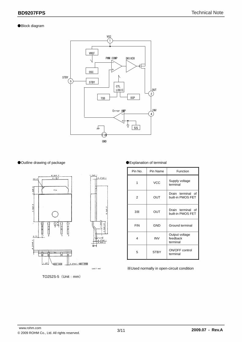
Block diagram
Outline drawing of package Explanation of terminal
※Used normally in open-circuit condition
Pin No. Pin Name Function
1 VCC Supply voltage terminal
2 OUT Drain terminal of built-in PMOS FET
3※ OUT Drain terminal of built-in PMOS FET
FIN GND Ground terminal
4 INV Output voltage feedback terminal
5 STBY ON/OFF control terminal
TO252S-5(Unit:mm)
SS
VREF
OSC
1
2
DRIVERPWM COMP
CTL
LOGIC
TSD
Error AMP4
INV
OUT
GND
STBY
5
VCC
OCP
STBY
FIN
Technical Note
4/11
BD9207FPS
www.rohm.com 2009.07 - Rev.A© 2009 ROHM Co., Ltd. All rights reserved.
Functional explanation of block
・ VREF
The constant voltage to be temperature-compensated is created from the voltage inputted from VCC terminal.
・ OSC
Triangular wave with an oscillating frequency of 900 KHz is created, as an input of PWM comparator, by built-in resistor
and capacitor.
・ Error AMP
It detects, at INC terminal, the voltage of sense resistance terminal created by LEC current, and compares it to the
reference voltage, and amplifies and outputs the differential voltage.
(The reference voltage is 0.2V±3%)
・ PWM COMP
PWM COMP converts the output voltage of error amplifier into the pulse-width modulation waveform and outputs it to
DRIVER.
・ DRIVER Push-pull FET driver takes in the PWM waveform and directly drives the Pch MOS FET that is built-in in the IC.
・ STBY
The ON/OFF control of output is performed by STBY terminal. The output becomes ON if STBY voltage is High level.
・ Thermal shutdown circuit (TSD)
TSD circuit protects the IC from runaway thermal operation or heat damage.
TSD circuit detects the temperature of chip, and the circuit becomes off if the temperature reaches 175. For TSD
detection and release, the hysteresis of 15 is set, so the malfunction caused by temperature variation is prevented.
・ Over Current Protection(OCP)
Out is turned off if the voltage difference between VCC – OUT, caused by the current flowing in the Pch MOS EFT built-in in OCP circuit, is detected and reaches the reference value of OCP. The OCP is not of latch type but of self-return type.
・ Soft start circuit (SS)
Soft start time is set by the built-in capacitor connected to SS circuit. The capacitor is charged when STBY terminal
becomes High level and the IC is started. The soft start time is set at 4ms or so.
Technical Note
5/11
BD9207FPS
www.rohm.com 2009.07 - Rev.A© 2009 ROHM Co., Ltd. All rights reserved.
Selection and setting of application parts
Coil L1
The application efficiency will decrease by the larger serial resistance element of coil. Moreover, because OCP operates by 1.6A(min) or more, so please notice the heat generated by overload output or short. Please set current ratings of coil with IOUT(MAX)+⊿IL or more. Iout(MAX): maximum load current
If current flows more than ratings current, then coil generates heat, magnetic saturation, and causes oscillation or low
efficiency.
Please select the peak current with enough margins not to exceed current rating of coil.
L1: Coil value,VCC: Input voltage,VOUT: Output voltage, ⊿IL: Ripple current, fosc: Oscillation frequency
When value the efficiency , we recommend C10-H5R(mitsumi) . Efficiency will be improved about 1~2%.
Schottky diode D1
Please select Schottky diode with lowest forward voltage VF. (We can suppress the dissipation of forward voltage descent, and raise the efficiency. ) Diode selection is based on maximum forward current rating, reverse voltage rating and permissible power dissipation of diode. ・The maximum current ratings are assumed more than the value of maximum load current+ coil ripple current(⊿IL).
・Reverse voltage rating is set to be VIN or more.
・Please choose the smallest one of reverse current IR.
Especially, IR grows at high temperature, and causes thermo runaway.
・Select the diode which permissible power dissipation within ratings. Diode power dissipation Pdi is shown below. Pdi=Iout(MAX)×Vf×(1-VOUT/VCC)
Iout(MAX): Load current. Vf: Forward voltage, VOUT: Output voltage, VCC: Input voltage
Output capacitor C1
Select the output capacitor with ESR met the following formula.
Moreover, permissible ripple current effective value of output capacity is calculated by the next formula, and use this value to select the capacitor with enough margins. IRMS =⊿IL/2√3 IRMS: Permissible ripple current effective value of output capacity, ⊿IL : Ripple current Ceramic capacitor must use the one more than B characteristic. Besides above mentioned, IC might not be normally operated according to the different setting condition of ambient temperature and output voltage. Moreover, even aluminum electrolytic capacitor can be used, please confirm its operation enough before using it.
Input capacitor C2
Input capacitor built in Pch MOS FET ON is the current supply of coil by FET. So, please close to IC as near as possible to connect it. Enough margins is taken on setting input capacitor in capacitor withstand voltage and permissible ripple current value. According to the ripple current effective value of input capacitor shown below, select the capacitor with enough permissible ripple current value.
IRMS : Permissible ripple current value of input capacitor
IOUT : Load current. VOUT: Output voltage, VCC: Input voltage
⊿IL. = L1
(VCC-VOUT) VOUT VCC fosc
1 × ×
IRMS=IOUT×√ (1-VOUT / VCC)×VOUT / VCC
ESR≦⊿VL/⊿IL
⊿VL : Permissible ripple voltage, ⊿IL : Ripple current
Technical Note
6/11
BD9207FPS
www.rohm.com 2009.07 - Rev.A© 2009 ROHM Co., Ltd. All rights reserved.
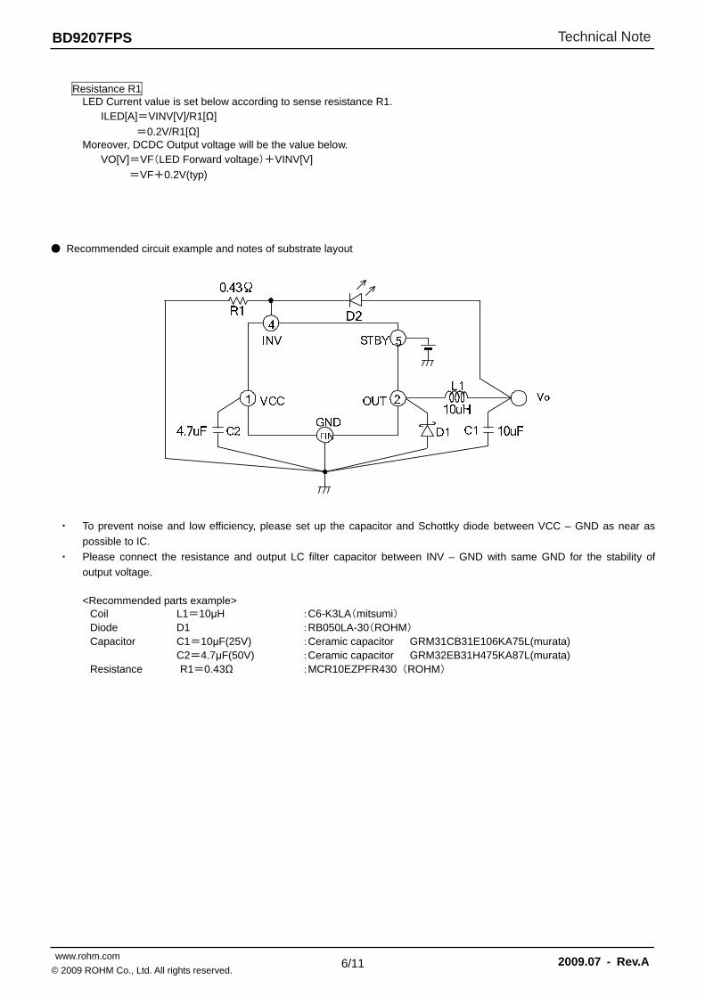
Resistance R1
LED Current value is set below according to sense resistance R1. ILED[A]=VINV[V]/R1[Ω]
=0.2V/R1[Ω] Moreover, DCDC Output voltage will be the value below.
VO[V]=VF(LED Forward voltage)+VINV[V]
=VF+0.2V(typ)
Recommended circuit example and notes of substrate layout
・ To prevent noise and low efficiency, please set up the capacitor and Schottky diode between VCC – GND as near as
possible to IC.
・ Please connect the resistance and output LC filter capacitor between INV – GND with same GND for the stability of
output voltage.
<Recommended parts example>
Coil L1=10μH :C6-K3LA(mitsumi) Diode D1 :RB050LA-30(ROHM) Capacitor C1=10μF(25V) :Ceramic capacitor GRM31CB31E106KA75L(murata) C2=4.7μF(50V) :Ceramic capacitor GRM32EB31H475KA87L(murata) Resistance R1=0.43Ω :MCR10EZPFR430(ROHM)

Technical Note
7/11
BD9207FPS
www.rohm.com 2009.07 - Rev.A© 2009 ROHM Co., Ltd. All rights reserved.
IINVIcc
Vcc
cccc
OUT GND INV STBY
Vcc
SW4 SW5SW2
1 2 FIN 4 5
A
Vo
f
A A
V
VINV
ISTB
VSTB
SW6
+
+
Io
0.43Ω
Measurement circuit diagram
Technical Note
8/11
BD9207FPS
www.rohm.com 2009.07 - Rev.A© 2009 ROHM Co., Ltd. All rights reserved.
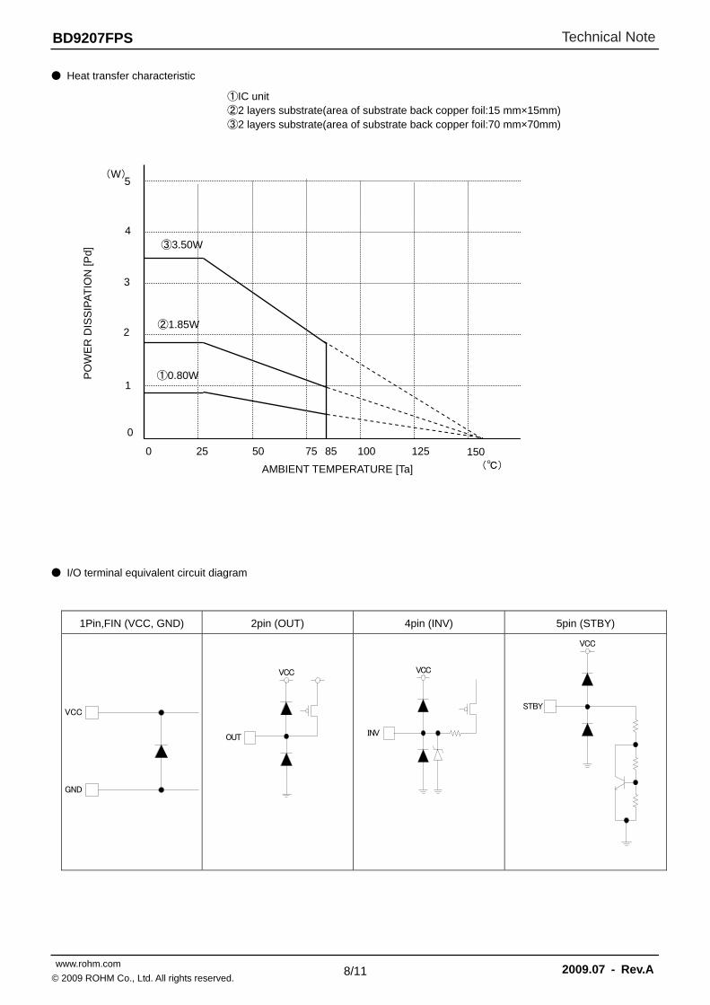
Heat transfer characteristic
I/O terminal equivalent circuit diagram
1Pin,FIN (VCC, GND) 2pin (OUT) 4pin (INV) 5pin (STBY)
PO
WE
R D
ISS
IPA
TIO
N [
Pd]
AMBIENT TEMPERATURE [Ta]
①IC unit ②2 layers substrate(area of substrate back copper foil:15 mm×15mm) ③2 layers substrate(area of substrate back copper foil:70 mm×70mm)
0
2
5
3
0 25 50 75 100 125 150()
①0.80W
②1.85W
1
4
85
③3.50W
(W)
VCC
GND
OUT
VCC
STBY
VCC
INV
VCC
Technical Note
9/11
BD9207FPS
www.rohm.com 2009.07 - Rev.A© 2009 ROHM Co., Ltd. All rights reserved.
Notes for use 1. We have paid enough attention to quality control of this product, but it may be destroyed when the absolute
maximum rating of impressed voltage and operating temperature range is exceeded. Because we can’t specify that is short-mode or open-mode etc while it is destroyed, so please discuss to give physical safety action with postulating the special mode exceeded absolute maximum rating.
2. About application circuit
Application circuit is recommended, but please fully confirm temperature characteristic etc when using it. Moreover, please acknowledge that our company can’t confirm enough about patent.
3. About the range of operation power-supply voltage
Circuit function operation at the range of operation ambient temperature is guaranteed when it is in the range of operation power-supply voltage. About characteristic value, the specification value of electric characteristic can’t be guaranteed, but the characteristic value doesn’t change rapidly in these ranges.
4. About ground connection
The ground connection shown in application circuit example should equip enough fat GND(FIN) to every ground
connection with shortest pattern drawing, and the pattern shouldn’t interfere the electric characteristic. 5. About input power-supply
The input power-supply shown in application circuit example should equip input pin VCC(1pin) with short enough pattern drawing, and the pattern shouldn’t interfere the electric characteristic.
6. Please think about permissible power dissipation (Pd) in an actual using status, and do the heat design with
enough margins. 7. Please pay enough attention to the direction and displacement of IC when you install it on PCB. If you install it by
mistake, IC might be destroyed, Moreover, when short-circuit happen by foreign substance entered between outputs, or output and power supply GND, it will be destroyed.
8. Please note that there is a possibility of malfunction if you use it in strong electromagnetic field. 9. Please set STBY terminal voltage to 0.3V or less when putting it on standby status, to 2.0V or more when putting it
on operation status. Please do not fix STBY terminal voltage from 0.3V to 2.0V. It may cause malfunction or breakdown.
Technical Note
10/11
BD9207FPS
www.rohm.com 2009.07 - Rev.A© 2009 ROHM Co., Ltd. All rights reserved.
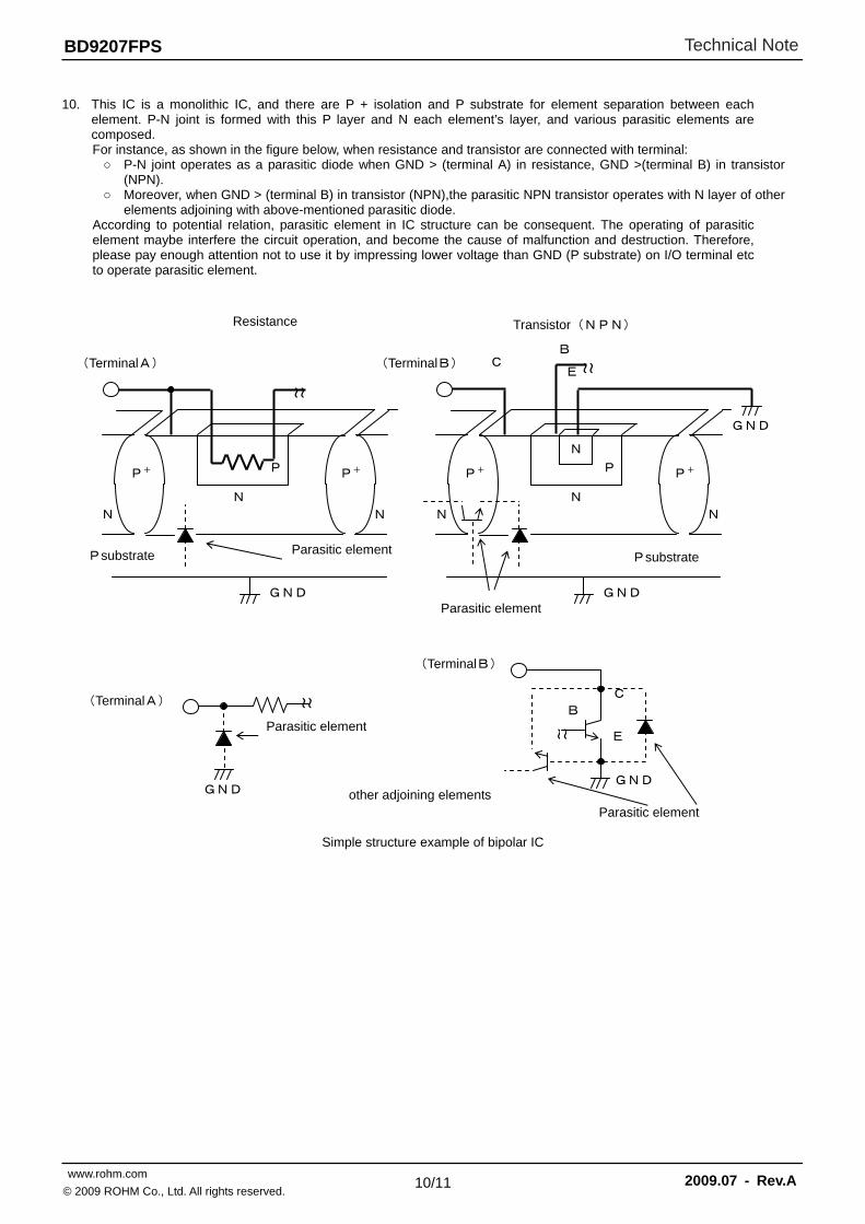
10. This IC is a monolithic IC, and there are P + isolation and P substrate for element separation between each
element. P-N joint is formed with this P layer and N each element’s layer, and various parasitic elements are composed. For instance, as shown in the figure below, when resistance and transistor are connected with terminal: P-N joint operates as a parasitic diode when GND > (terminal A) in resistance, GND >(terminal B) in transistor
(NPN). Moreover, when GND > (terminal B) in transistor (NPN),the parasitic NPN transistor operates with N layer of other
elements adjoining with above-mentioned parasitic diode. According to potential relation, parasitic element in IC structure can be consequent. The operating of parasitic element maybe interfere the circuit operation, and become the cause of malfunction and destruction. Therefore, please pay enough attention not to use it by impressing lower voltage than GND (P substrate) on I/O terminal etc to operate parasitic element.
Simple structure example of bipolar IC
~
~
GND
Psubstrate
N
P
N N
P+ P+
(TerminalA)
Resistance
~
~
GND
N
P
N N
P+ P+
(TerminalB)
Transistor(NPN)
B
N
E C
GND
~
~
(TerminalA)
GND
Parasitic element
~ ~
GND
(TerminalB)
B C
E
Psubstrate Parasitic element
Parasitic element
Parasitic element other adjoining elements
Technical Note
11/11
BD9207FPS
www.rohm.com 2009.07 - Rev.A© 2009 ROHM Co., Ltd. All rights reserved.
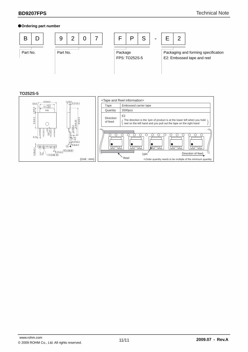
Ordering part number
B D 9 2 0 7 F P S - E 2
Part No. Part No.
Package
FPS: TO252S-5
Packaging and forming specification
E2: Embossed tape and reel
(Unit : mm)
TO252S-5
S
0.08 M
0.08 S
+64 –4
1 2
3
54
0.8
0.71
C0.56.5±0.2
5.1+0.2−0.1
5.5±
0.2
1.5±
0.2
FIN
0.27±0.1
1.0±
0.2
2.5±
0.15
9.5±
0.3
1.2±0.10.27±0.1
0.6±0.2
0.27±0.11.270.
35±0
.1
Direction of feed1pinReel ∗ Order quantity needs to be multiple of the minimum quantity.
<Tape and Reel information>
Embossed carrier tapeTape
Quantity
Direction of feed
The direction is the 1pin of product is at the lower left when you hold reel on the left hand and you pull out the tape on the right hand
2000pcs
E2
( )
DatasheetDatasheet
Notice - GE Rev.002© 2014 ROHM Co., Ltd. All rights reserved.
Notice Precaution on using ROHM Products
1. Our Products are designed and manufactured for application in ordinary electronic equipments (such as AV equipment, OA equipment, telecommunication equipment, home electronic appliances, amusement equipment, etc.). If you intend to use our Products in devices requiring extremely high reliability (such as medical equipment (Note 1), transport equipment, traffic equipment, aircraft/spacecraft, nuclear power controllers, fuel controllers, car equipment including car accessories, safety devices, etc.) and whose malfunction or failure may cause loss of human life, bodily injury or serious damage to property (“Specific Applications”), please consult with the ROHM sales representative in advance. Unless otherwise agreed in writing by ROHM in advance, ROHM shall not be in any way responsible or liable for any damages, expenses or losses incurred by you or third parties arising from the use of any ROHM’s Products for Specific Applications.
(Note1) Medical Equipment Classification of the Specific Applications JAPAN USA EU CHINA
CLASSⅢ CLASSⅢ
CLASSⅡb CLASSⅢ
CLASSⅣ CLASSⅢ
2. ROHM designs and manufactures its Products subject to strict quality control system. However, semiconductor
products can fail or malfunction at a certain rate. Please be sure to implement, at your own responsibilities, adequate safety measures including but not limited to fail-safe design against the physical injury, damage to any property, which a failure or malfunction of our Products may cause. The following are examples of safety measures:
[a] Installation of protection circuits or other protective devices to improve system safety [b] Installation of redundant circuits to reduce the impact of single or multiple circuit failure
3. Our Products are designed and manufactured for use under standard conditions and not under any special or extraordinary environments or conditions, as exemplified below. Accordingly, ROHM shall not be in any way responsible or liable for any damages, expenses or losses arising from the use of any ROHM’s Products under any special or extraordinary environments or conditions. If you intend to use our Products under any special or extraordinary environments or conditions (as exemplified below), your independent verification and confirmation of product performance, reliability, etc, prior to use, must be necessary:
[a] Use of our Products in any types of liquid, including water, oils, chemicals, and organic solvents [b] Use of our Products outdoors or in places where the Products are exposed to direct sunlight or dust [c] Use of our Products in places where the Products are exposed to sea wind or corrosive gases, including Cl2,
H2S, NH3, SO2, and NO2
[d] Use of our Products in places where the Products are exposed to static electricity or electromagnetic waves [e] Use of our Products in proximity to heat-producing components, plastic cords, or other flammable items [f] Sealing or coating our Products with resin or other coating materials [g] Use of our Products without cleaning residue of flux (even if you use no-clean type fluxes, cleaning residue of
flux is recommended); or Washing our Products by using water or water-soluble cleaning agents for cleaning residue after soldering
[h] Use of the Products in places subject to dew condensation
4. The Products are not subject to radiation-proof design. 5. Please verify and confirm characteristics of the final or mounted products in using the Products. 6. In particular, if a transient load (a large amount of load applied in a short period of time, such as pulse. is applied,
confirmation of performance characteristics after on-board mounting is strongly recommended. Avoid applying power exceeding normal rated power; exceeding the power rating under steady-state loading condition may negatively affect product performance and reliability.
7. De-rate Power Dissipation (Pd) depending on Ambient temperature (Ta). When used in sealed area, confirm the actual
ambient temperature. 8. Confirm that operation temperature is within the specified range described in the product specification. 9. ROHM shall not be in any way responsible or liable for failure induced under deviant condition from what is defined in
this document.
Precaution for Mounting / Circuit board design 1. When a highly active halogenous (chlorine, bromine, etc.) flux is used, the residue of flux may negatively affect product
performance and reliability. 2. In principle, the reflow soldering method must be used; if flow soldering method is preferred, please consult with the
ROHM representative in advance. For details, please refer to ROHM Mounting specification
DatasheetDatasheet
Notice - GE Rev.002© 2014 ROHM Co., Ltd. All rights reserved.
Precautions Regarding Application Examples and External Circuits 1. If change is made to the constant of an external circuit, please allow a sufficient margin considering variations of the
characteristics of the Products and external components, including transient characteristics, as well as static characteristics.
2. You agree that application notes, reference designs, and associated data and information contained in this document
are presented only as guidance for Products use. Therefore, in case you use such information, you are solely responsible for it and you must exercise your own independent verification and judgment in the use of such information contained in this document. ROHM shall not be in any way responsible or liable for any damages, expenses or losses incurred by you or third parties arising from the use of such information.
Precaution for Electrostatic
This Product is electrostatic sensitive product, which may be damaged due to electrostatic discharge. Please take proper caution in your manufacturing process and storage so that voltage exceeding the Products maximum rating will not be applied to Products. Please take special care under dry condition (e.g. Grounding of human body / equipment / solder iron, isolation from charged objects, setting of Ionizer, friction prevention and temperature / humidity control).
Precaution for Storage / Transportation 1. Product performance and soldered connections may deteriorate if the Products are stored in the places where:
[a] the Products are exposed to sea winds or corrosive gases, including Cl2, H2S, NH3, SO2, and NO2 [b] the temperature or humidity exceeds those recommended by ROHM [c] the Products are exposed to direct sunshine or condensation [d] the Products are exposed to high Electrostatic
2. Even under ROHM recommended storage condition, solderability of products out of recommended storage time period may be degraded. It is strongly recommended to confirm solderability before using Products of which storage time is exceeding the recommended storage time period.
3. Store / transport cartons in the correct direction, which is indicated on a carton with a symbol. Otherwise bent leads
may occur due to excessive stress applied when dropping of a carton. 4. Use Products within the specified time after opening a humidity barrier bag. Baking is required before using Products of
which storage time is exceeding the recommended storage time period.
Precaution for Product Label QR code printed on ROHM Products label is for ROHM’s internal use only.
Precaution for Disposition When disposing Products please dispose them properly using an authorized industry waste company.
Precaution for Foreign Exchange and Foreign Trade act Since our Products might fall under controlled goods prescribed by the applicable foreign exchange and foreign trade act, please consult with ROHM representative in case of export.
Precaution Regarding Intellectual Property Rights 1. All information and data including but not limited to application example contained in this document is for reference
only. ROHM does not warrant that foregoing information or data will not infringe any intellectual property rights or any other rights of any third party regarding such information or data. ROHM shall not be in any way responsible or liable for infringement of any intellectual property rights or other damages arising from use of such information or data.:
2. No license, expressly or implied, is granted hereby under any intellectual property rights or other rights of ROHM or any
third parties with respect to the information contained in this document.
Other Precaution 1. This document may not be reprinted or reproduced, in whole or in part, without prior written consent of ROHM. 2. The Products may not be disassembled, converted, modified, reproduced or otherwise changed without prior written
consent of ROHM. 3. In no event shall you use in any way whatsoever the Products and the related technical information contained in the
Products or this document for any military purposes, including but not limited to, the development of mass-destruction weapons.
4. The proper names of companies or products described in this document are trademarks or registered trademarks of
ROHM, its affiliated companies or third parties.
DatasheetDatasheet
Notice – WE Rev.001© 2014 ROHM Co., Ltd. All rights reserved.
General Precaution 1. Before you use our Pro ducts, you are requested to care fully read this document and fully understand its contents.
ROHM shall n ot be in an y way responsible or liabl e for fa ilure, malfunction or acci dent arising from the use of a ny ROHM’s Products against warning, caution or note contained in this document.
2. All information contained in this docume nt is current as of the issuing date and subj ect to change without any prior
notice. Before purchasing or using ROHM’s Products, please confirm the la test information with a ROHM sale s representative.
3. The information contained in this doc ument is provi ded on an “as is” basis and ROHM does not warrant that all
information contained in this document is accurate an d/or error-free. ROHM shall not be in an y way responsible or liable for any damages, expenses or losses incurred by you or third parties resulting from inaccuracy or errors of or concerning such information.