lecture: diannao and dadiannao
TRANSCRIPT

1
Lecture: DianNao and DaDianNao
• Topics: Diannao wrap-up and DaDianNao

2
DaDianNao Philosophy
• Need giga-bytes of storage for weights and accessing theseweights is the clear bottleneck
• Can’t store giga-bytes on 1 chip, but can store giga-byteson many chips on a board
• Surround a DianNao circuit with a large eDRAM (dense)structure to replace main memory (high storage-to-compute)
• Every operation is spread across several “tiles” to maximizeparallelism
DaDianNao tries to avoid going to off-chip memory altogether. It keeps the weights on-chip in eDRAM banks (eDRAM is a denser technology than SRAM). But one chip may not be enough. So you use as many chips as required to keep all the weights in on-chip eDRAM banks.
3
DaDianNao Philosophy
Even on a single DaDianNao chip, we can implement multiple tiles. Each tile has an NFU (like the one we discussed for DianNao), and an adjacent eDRAM bank. So, we have a distributed architecture, spread across many DaDianNao chips. We perform Near Data Processing, i.e., a computation is performed on the NFU next to the eDRAM that has the necessary weight. The computation for a layer is scattered across all available tiles. For example, if there are T tiles and N neurons, each tile is responsible for N/T neurons and all the weights for that neuron are stored in that local tile. When those neurons produce their output, they are broadcast to all the tiles that need these as inputs to the next layer (through central eDRAM buffers).Each tile has 4 512KB eDRAM banks to store its weights. A chip has 16 tiles and these tiles share 2 2MB eDRAM banks to store the inputs from the previous layer and the outputs of the current layer. So a DaDianNao chip has (significant) total storage of 36MB (32MB for synaptic weights). Recall that the NFU needs to receive 512 B/cycle to stay busy during the classifier layer. To provide this high bandwidth while tolerating the 3 cycle eDRAM latency (at ~600 MHz freq), they use 4 eDRAM banks. That is, they go through each eDRAM bank in round-robin fashion. Each eDRAM bank therefore has a read width of 512 bytes, which is a *lot* of wiring overhead. They are essentially dealing with the memory bandwidth problem by provisioning a lot of on-chip wiring (which does cost them in terms of chip area).

4
DaDianNao Philosophy II
• Synapses stay in place and neuron values move around(since synapses are so much larger)
• Use eDRAM instead of SRAM (about 2.85x higher density)
• Can get high internal bandwidth by having many banksfor eDRAM storage (they use 4)
• Implement many tiles on a chip – each tile has 4 eDRAMbanks for weights, and all tiles share 2 eDRAM banksfor input/output
• They allow 32-bit operations because it is useful for training

5
DaDianNao Layouts
Each eDRAM bank size is 512 KB (3 cyc); central eDRAM bank is2MB (10 cyc); total node storage is 36 MB; HT bw is 6.4 x 4 GB/s (80ns).

6
Other Details
• 606 MHz clock (because of the eDRAM)• 5.58 Tera ops/second• 16 W node (chip), 68 mm2
• Area breakdown: 45% tiles; 26% HT; 12% central eDRAM;9% central wiring
• Half the chip is eDRAM storage• Power breakdown: 39% in tiles, 50% HT; eDRAM power
is 38%; combinational circuits are 38%, 19% is registers
If you assume that every multiplier and every adder is producing a new value every cycle, you get a peak throughput of nearly 6 TOPs. The chip has modest size and power consumption. Note the breakdowns above. Note the significant speedups and energy reductions relative to a GPU on the next slides. All these improvements are because they are eliminating the memory access bottleneck.
7
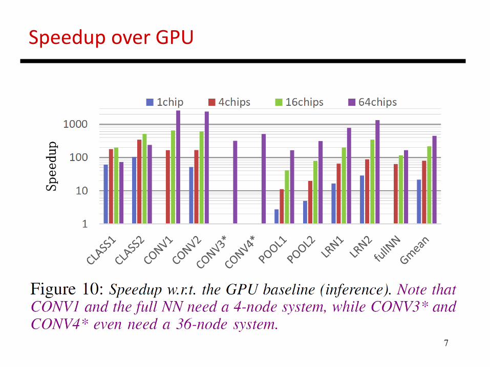
Speedup over GPU

8
Energy Reductions

9
Benchmarks
10
DaDianNao Summary
• Memory bandwidth is the key bottleneck, especiallywhen handling the fully-connected classifier layers
• DaDianNao manages this by distributing weights acrosseDRAM banks in many chips
• A layer is executed in parallel across several NFUs/chips;outputs are moved around; the next layer then executes(no memory accesses for weights)

11
Cerebras Wafer Scale Integration
Source: Cerebras.net
Trillion transistors18 GB SRAM15-50 KW power100 Pb/s internal bandwidth
12
Cerebras Wafer Scale Integration
See the August 29th blog post (that’s today!) on sigarch.org/blog about the Cerebras chip. This is the first trillion transistor package. The design philosophy for Cerebras is similar to that of DaDianNao. They are trying to pack the entire neural network model onto a number of chips. But instead of having separate packages that connect with HT, Cerebras uses WSI, i.e., an entire wafer is produced and is not sliced into dies. The metal layers are used to communicate between the dies. The overall SRAM capacity on the wafer is 18GB. The intra-wafer bandwidth is 100 Pb/s. They also have significant support for sparsity (details not currently available). Will dissipate 15-50 KW.

13
References
• “DianNao: A Small-Footprint High-Throughput Accelerator for UbiquitousMachine Learning”, T. Chen et al., Proceedings of ASPLOS, 2014
• “DaDianNao: A Machine-Learning Supercomputer”,Y. Chen et al., Proceedings of MICRO, 2014
• https://www.cerebras.net/wp-content/uploads/2019/08/Cerebras-Wafer-Scale-Engine-Whitepaper.pdf
• https://www.sigarch.org/the-first-trillion-transistor-chip-a-new-design-space