lecture 16 rc architecture types & fpga interns lecturer: simon winberg attribution-sharealike...
TRANSCRIPT

Lecture 16RC Architecture Types &
FPGA InternsLecturer:
Simon Winberg
Digital Systems
EEE4084F
Attribution-ShareAlike 4.0 International (CC BY-SA 4.0)
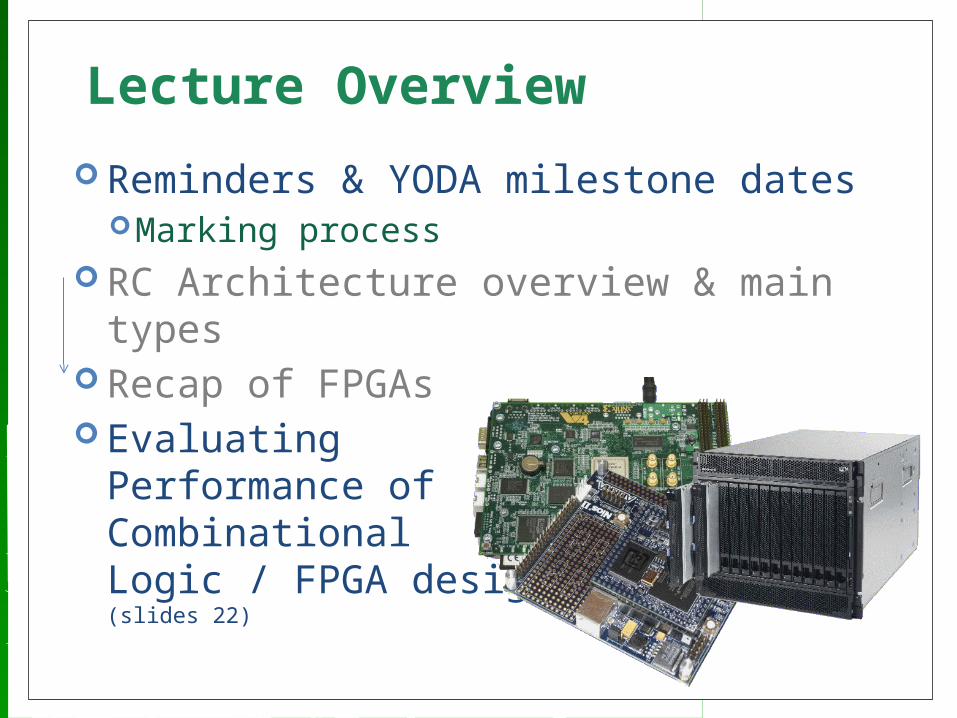
Lecture Overview
Reminders & YODA milestone datesMarking process
RC Architecture overview & main types
Recap of FPGAs Evaluating
Performance ofCombinationalLogic / FPGA design(slides 22)

Reminder
Indicate your YODA team in the Wiki. Add a blog entry to describe your topic
29 Apr – Blog about your product 15 May – Design Review 18-20 May – Demos 22 May final report & code (although
no late penalty if submitted before 25 May 8am)
See “EEE4084F YODA Mark Allocation Schema.pptx” for process of allocating marks for mark categories

YODA Report Marking process
Assignment work is marked in relation toCorrectnessCompletionStructure, effectiveness of wording & layoutAdequate amount of detail/results shown &
effectively dealing with the details Indication of student’s understanding and
engagement with the disciplineClarity of explanations/motivation of resultsProfessionalism and overall quality

RC Architectures OverviewReconfigurable Computing

Is it or isn’t it reconfigurable…?
A determining factor is ability to change hardware datapaths and control flows by software control
This change could be either a post-process / compile time or dynamically during runtime (doesn’t have to be both)
processingelements
Datapath
While the trivial case (a computer with one changeable datapath could be argued as being reconfigurable) it is usually assumed the computer system concerned has many changeable datapaths.
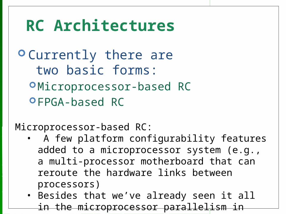
RC Architectures
Currently there are two basic forms:Microprocessor-based RCFPGA-based RC
Microprocessor-based RC:• A few platform configurability features added to a
microprocessor system (e.g., a multi-processor motherboard that can reroute the hardware links between processors)
• Besides that we’ve already seen it all in the microprocessor parallelism in part of the course

RC Architectures– basic forms
Microprocessor based RC Multi-core processors dynamically
joined to create a larger/smallerparallel system when needed
Assumed to be a single computer platform as apposed to a cluster of computers
Needs to support software-controlled dynamic reconfiguration (see previous slide)
Tends to become:Hardware essentially changeable in big blocks(“macro-level reconfiguration” - whole processors at a time)

RC Architectures– basic forms
FPGA basedGenerally much smaller level of
interconnects (more at the “micro-level reconfiguration”)
Processors that connect to FPGA(s)

General Architecture for using FPGA-based RC
Generally, these systems follow a processors + coprocessors arrangementCPU connectors to reprogrammable
hardware (usually FPGAs)The CPU itself may be
entirely in an FPGA The lower-level
architecture is moreinvolved…
CPU
FPGA-based Accelerator
card
…
high-speed bus
CPU…
FPGA-based Accelerator
card
Multi-processor o
r
multi-core processor
computer
Plug-in cardstopic of Seminar #8 (‘Interconnection Fabrics’) and further discussed in later lectures.

FPGA Interns
EEE4084F
Skip to slide 22; already covered in text book but scan through these slides to ensure you are well versed in these issues.

FPGA internal structure
Programmableinterconnect
Programmablelogic blocks
Image adapted from Maxfield (2004)
Programmable logic element (PLE)
(or FPLE*)
* FPLE = Field Programmable Logic Element
Note: one programmable logic block (PLB) may contain a complex arrangement of programmable logic elements (PLE).
The size of a FPGA or programmable logic device (PLD) is measured in the number of LEs (i.e., Logic Elements) that it has.

Logic Elements– Remember your logic primitives
You already know all your logic primitives…The primitive logic gates
AND, OR, NOR, NOT, NOR, NAND, XORAND3, OR4, etc (for multiple inputs).
Pins / sources / terminatorsGround, VCCInput, output
Storage elementsJK Flip FlopsLatches
Others items: delay, mux
OR
Input Pin
Output Pin
Altera Quartus II representations

Look Up Tables (LUTs)
A simple but powerful approach to FPGA design is to use lookup tables for the PLBs. These are usually implemented as a combination of a multiplexer and memory (even just using NOR gates)
Essentially, this approach is building complex circuits using truth tables (where each LUT enumerates a truth table)
The usual strategy for implementing PLBs
examples follows…
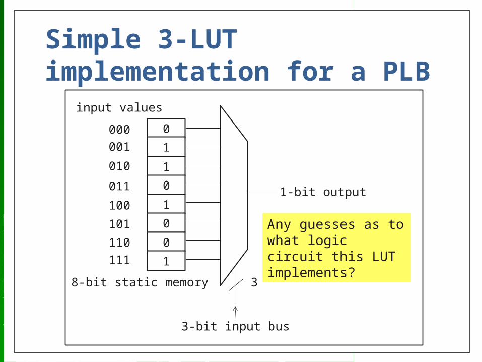
Simple 3-LUT implementation for a PLB
0
1
1
0
1
0
0
1
8-bit static memory 3
3-bit input bus
1-bit output
000
001
010
011
100
101
110
111
Any guesses as to what logic circuit this LUT implements?
input values

Simple 3-LUT implementation for a PLB
input lines
It’s an XOR of the 3 input lines!!!
output 0
1
1
0
1
0
0
1
000
001
010
011
100
101
110
111
in out

Mainstream* Programmable Logic Block (PLB)
k-input LUT
DFFclock
…k inputs output
config_sync
Configure synchronous or asynchronous response (i.e. a line from another big LUT).
0
1
Image adapted from Maxfield (2004)
Another example for implementing an alternate logic function.
* Used by manufacturers like Xilinx

Logic block clusters (LBCs) and Configurable logic blocks (CLBs)• Assume a k-input LUT for each logic block (LB)• Assume N x LBs per logic cluster• BLEs in each logic clusters are fully connected or mostly
connected
Diagram adapted from Sherief Reda (2007), EN2911X Lecture 2 Fall07, Brown University
The diagram shows the same input lines (I) are sent to each LB, in addition to each of the N LBs’ output lines. Each LB operates on 4 input lines at a time, and a MUX is used to decide which input to sample. The MUXs may be configured from a separate LUT, or could be controlled by the LB it is connected to.
LB
LB
…N x LBs

“Every slice contains four logic-function generators (or LUTs), eight storage elements, wide-function multiplexers, and carry logic. These elements are used by all slices to provide logic, arithmetic, and ROM functions. In addition to this, some slices supporttwo additional functions: storing data using distributed RAM and shifting data with 32-bit registers. Slices that support these additional functions are called SLICEM; others are called SLICEL. SLICEM represents a superset of elements and connections found in all slices. Each CLB can contain zero or one SLICEM. Every other CLB column contains a SLICEMs.In addition, the two CLB columns to the left of the DSP48E columns both contain a SLICELand a SLICEM.”
Xilinx L and M Slices Approachfor configurable logic blocks (CLBs)
Source: http://www.xilinx.com/support/documentation/user_guides/ug364.pdf pg 8

SLICEM slices support additional functions; they are a superset of SLICELs; i.e. the have all the standard LEs plus some additions.
Source: http://www.xilinx.com/support/documentation/user_guides/ug364.pdf pg 9

SLICEL slices contain the standard set of LEs for the particular FPGA concerned. As the diagram shows, it looks a little less complicated than the design of a SLICEM.
Source: http://www.xilinx.com/support/documentation/user_guides/ug364.pdf pg 10

Evaluating PerformanceEvaluating synthesis (simplified) of an FPGA design

HDL to FPGA execution & LE cost
Map ‘AND(e,f,g)’ to LB1
In order to implement a HDL design, the design need to be decomposed and mapped to the physical LBs on the FPGA and the interconnects need to be appropriately configured.
Example: x = AND(e,f,g) y = AND(b,NAND(NAND(b,c),d)) out = NAND((NAND(x,y),NAND(a,y))
out
xy
Map ‘NAND((NAND(x,y),NAND(a,y))’ to LB2
Map ‘AND(b,NAND(NAND(b,c),d)) ’ to LB3
Costing: 3 LBs, 8 LEs (assuming LBs have LEs that are AND or NAND gates)

Timing calculations The previous slide didn’t show whether the
connections were synchronized (i.e., a shared clock) or asynchronous –since they are all logic gates and no clocks show it’s probably asynchronous
Determining the timing constrains for synchronous configurations are generally easier, because everything is related to the clock speed. Still, you need to keep in mind cascading calculations.
For asynchronous use, the implementation could run faster, but can also become a more complicated design, and be more difficult to work out the timing…

Async Timing calculations Keep in mind that the propagation delays for the
various gates / LUTs may be different – for example, in the previous example, let’s assume each AND may take 6ns to stabilise, and the NANDS 10ns.
So time to compute out is =
MAX OF (time to compute x, time to compute y) + 2x10ns
= (2x10ns+6ns) + 20ns = 46ns = pretty fast!! Or is it??
Compared to a 1GHz CPU using just registers (and no
mem access)?
Try this calculation for yourself ... (assume each instruction takes on avg. 3 clocks due to pipeline, data dependencies, etc, as worst case performance on a RISC processor)

Comparing to CPU speedCPU running at 1GHz each clock 1ns periodAssume each instruction takes ~ 5 clocks each due to pipeline etcCODE:int doit ( unsigned a, b, c, d, e, f, g ) { unsigned x = AND(e,f,g); unsigned y = AND(b,NAND(NAND(b,c),d)) out = NAND((NAND(x,y),NAND(a,y)) return out;}
unsigned t1 = AND(e,f); 1 instruction, i.e. AND t1,e,f unsigned x = AND(t1,g);unsigned t1 = NAND(b,c)unsigned t2 = NAND(t1,d)unsigned y = AND(b,t2) t1 = NAND(x,y)t2 = NAND(a,y)out = NAND(t1,t2)
in all 8 instructions 8 x 3 clocks ea. = 24 ns (assuming all registers pre-loaded) A speed-up of 1.92 over the FPGA case
But some of theseCan’t be done as just 1RISC instruction.

Plans for Next lecture
RC architecture case studies IBM Blade & the cell processorSome large-scale RC systems
Amdahl’s Law reviewed and critiqued

Image sources:FYI Stamp – Wikipedia open commonsReminder stamp – Open Clipart www.openclipart.org (public domain)Xilinx FPGA related images & schematics – from Xilinx datasheets or their website
Disclaimers and copyright/licensing details
I have tried to follow the correct practices concerning copyright and licensing of material, particularly image sources that have been used in this presentation. I have put much effort into trying to make this material open access so that it can be of benefit to others in their teaching and learning practice. Any mistakes or omissions with regards to these issues I will correct when notified. To the best of my understanding the material in these slides can be shared according to the Creative Commons “Attribution-ShareAlike 4.0 International (CC BY-SA 4.0)” license, and that is why I selected that license to apply to this presentation (it’s not because I particulate want my slides referenced but more to acknowledge the sources and generosity of others who have provided free material such as the images I have used).