lecture 16 bipolar junction transistor...
TRANSCRIPT

Lecture 16
Bipolar Junction Transistor (BJT)
BJT 1-1

Outline Continue BJT analysis with AC signal
Common-Emitter and Emitter-Follower configurations • Analysis using various biasing circuits
Effect of source/load impedance on current and voltage gain
BJT 1-2

BJT
BJT 1-3

Why DC bias for BJT
BJT 1-4
linear and nonlinear operation of an inverting amplifier

BJT as an amplifier
BJT 1-5

Common-Emitter Configuration
BJT 1-6
bbe III 1
The diode re model can be replaced by the resistor re.
e
eI
mV 26r

Common-Emitter Configuration
BJT 1-7
Input impedance:
Output impedance:
Voltage gain:
Current gain:
e
B
ii rZIV
oo rZ
e
LV
r
RA VV
i
o
oriA
IIi
o
RL
Vo

Common-Emitter Configuration
BJT 1-8
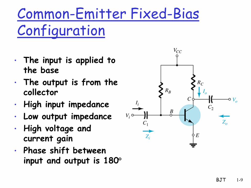
Common-Emitter Fixed-Bias Configuration
BJT 1-9
• The input is applied to the base
• The output is from the collector
• High input impedance
• Low output impedance
• High voltage and current gain
• Phase shift between input and output is 180

Common-Emitter Fixed-Bias Configuration
BJT 1-10
AC equivalent
re model
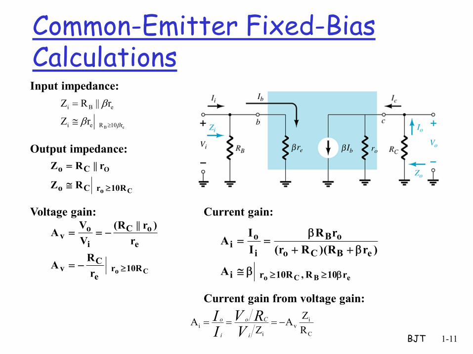
Common-Emitter Fixed-Bias Calculations
BJT 1-11
Co 10Rre
Cv
e
oC
i
ov
r
RA
r
)r||(R
V
VA
eBCo r10R ,10Rri
eBCo
oB
i
oi
A
)r)(RR(r
rR
I
IA
C
iv
i
iR
ZA
ZA
VRV
II
i
Co
i
o
Current gain from voltage gain:
Input impedance:
Output impedance:
Voltage gain: Current gain:
eB r10Rei
eBi
rZ
r||RZ
Co
O
R10rCo
Co
RZ
r||RZ

Common-Emitter Voltage-Divider Bias Configuration
BJT 1-12
AC equivalent circuit using the re model

Common-Emitter Voltage-Divider Bias Calculations
BJT 1-13
Current gain from voltage gain:
Input impedance:
Output impedance:
Voltage gain:
Current gain:
ei
21
r||RZ
R||RR
Co 10RrCo
oCo
RZ
r||RZ
Co 10Rre
C
i
ov
e
oC
i
ov
r
R
V
VA
r
r||R
V
VA
eCo
Co
r10R ,10Rri
oi
10Rrei
oi
eCo
o
i
oi
I
IA
rR
R
I
IA
)rR)(R(r
rR
I
IA
C
ivi
R
ZAA
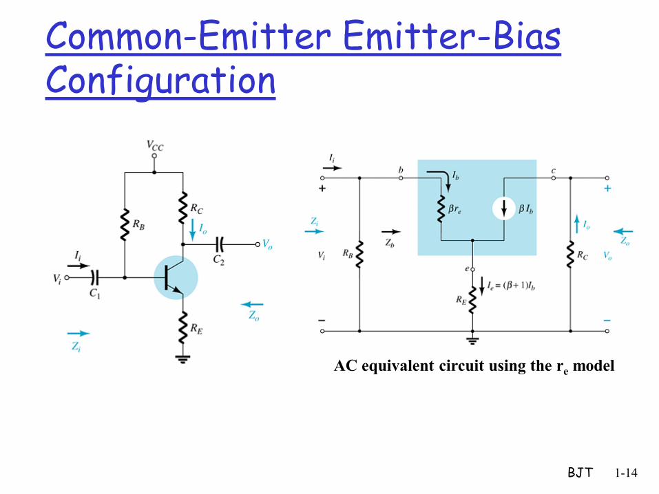
Common-Emitter Emitter-Bias Configuration
BJT 1-14
AC equivalent circuit using the re model

Common-Emitter Emitter-Bias Calculations
BJT 1-15
Eb
Eeb
Eeb
bBi
RZ
)R(rZ
1)R(rZ
Z||RZ
Input impedance:
Output impedance:
Co RZ
Voltage gain:
Eb
Eeb
RZE
C
i
ov
)R(rZEe
C
i
ov
b
C
i
ov
R
R
V
VA
Rr
R
V
VA
Z
R
V
VA
Current gain:
bB
B
i
oi
ZR
R
I
IA
Current gain from voltage gain:
C
ivi
R
ZAA

Example
BJT 1-16
For the CE Emitter-Bias Configuration circuit: (a) Determine re. (b) Find Zi and Zo. (c) Calculate Av and Ai.

Solution
BJT 1-17

Emitter-Follower Configuration
BJT 1-18
• This is also known as the common-collector configuration.
• The input is applied to the base and the output is taken from the
emitter.
• There is no phase shift between input and output.

Emitter-Follower Configuration Calculations
BJT 1-19
Input impedance:
Output impedance:
Current gain from voltage gain:
Voltage gain:
Current gain:
Eb
Eeb
Eeb
bBi
RZ
)R(rZ
1)R(rZ
Z||RZ
eE rReo
eEo
rZ
r||RZ
EeEeE RrR ,rRi
ov
eE
E
i
ov
1V
VA
rR
R
V
VA
bB
Bi
ZR
RA
E
ivi
R
ZAA

Table of Comparison
BJT 1-20

Take Home Problem
Determine the signal peak voltage at the base (Vb) of the transistor in the figure. This circuit shows a signal source of 10 mV rms. IE was previously found to be 3.80 mA
BJT 1-21
Vb

Effect of Load Impedance on Gain (Two-Port Systems Approach)
BJT 1-22 L
ivi
R
RAA
- This model can be applied to any current- or voltage-controlled amplifier.
vNL
oL
L
i
ov A
RR
R
V
VA
where AvNL is the no-load voltage gain
- Adding a load reduces the gain of the amplifier:

Effect of Source Impedance on Gain (Two-Port Systems Approach)
BJT 1-23
- The fraction of applied signal that reaches the input of the amplifier is:
- The internal resistance of the signal source reduces the overall gain:
si
sii
RR
VRV
vNLsi
i
s
ovs A
RR
R
V
VA

Combined Effects of source and load Impedance on Voltage Gain
BJT 1-24
Effects of RL and RS:
L
isvsis
vNLoL
L
si
i
s
ovs
R
RRAA
ARR
R
RR
R
V
VA

BJT 1-25
Lecture Summary
Covered material Continue BJT analysis with small AC signal
Common-Emitter and common-collector configurations • Analysis using various biasing circuits
Effect of source/load impedance on current and voltage gain
Material to be covered next lecture
Introduction to FET