lecture 070 – resistors and inductors
TRANSCRIPT
Lecture 070 – Resistors and Inductors (4/19/10) Page 070-1
CMOS Analog Circuit Design © P.E. Allen - 2010
LECTURE 070 – RESISTORS AND INDUCTORSLECTURE ORGANIZATION
Outline• Resistors• Inductors• SummaryCMOS Analog Circuit Design, 2nd Edition ReferencePages 47-48, 60-63 and new material
Lecture 070 – Resistors and Inductors (4/19/10) Page 070-2
CMOS Analog Circuit Design © P.E. Allen - 2010
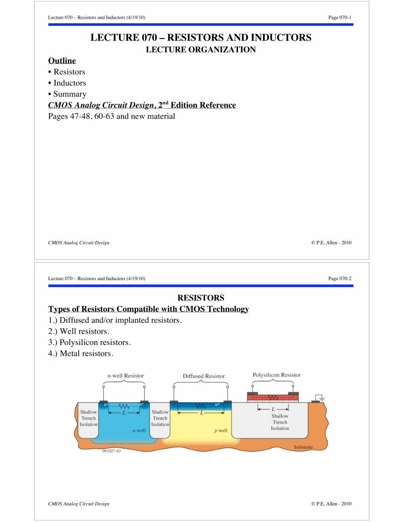
RESISTORSTypes of Resistors Compatible with CMOS Technology1.) Diffused and/or implanted resistors.2.) Well resistors.3.) Polysilicon resistors.4.) Metal resistors.
Lecture 070 – Resistors and Inductors (4/19/10) Page 070-3
CMOS Analog Circuit Design © P.E. Allen - 2010
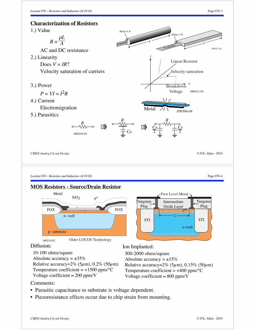
Characterization of Resistors1.) Value
R = L
AAC and DC resistance
2.) LinearityDoes V = IR?Velocity saturation of carriers
3.) Power
P = VI = I2R4.) Current
Electromigration5.) Parasitics
060210-01
R
Cp
R
Cp2
Cp2
R
L
Area = A
Current
050217-02
L
Area = A
Current
060211-01
i
v
Linear Resistor
Velocity saturation
BreakdownVoltage
Metal050304-04
Lecture 070 – Resistors and Inductors (4/19/10) Page 070-4
CMOS Analog Circuit Design © P.E. Allen - 2010
MOS Resistors - Source/Drain Resistor
060214-02
p- substrate
FOX FOX
SiO2Metal
n- well
p+
Older LOCOS Technology
p+
n-well
p+
STIL
TungstenPlug
IntermediateOxide Layer
TungstenPlug
First Level Metal
STI
Diffusion:10-100 ohms/squareAbsolute accuracy = ±35%Relative accuracy=2% (5μm), 0.2% (50μm)Temperature coefficient = +1500 ppm/°CVoltage coefficient 200 ppm/V
Ion Implanted:500-2000 ohms/squareAbsolute accuracy = ±15%Relative accuracy=2% (5μm), 0.15% (50μm)Temperature coefficient = +400 ppm/°CVoltage coefficient 800 ppm/V
Comments:• Parasitic capacitance to substrate is voltage dependent.• Piezoresistance effects occur due to chip strain from mounting.
Lecture 070 – Resistors and Inductors (4/19/10) Page 070-5
CMOS Analog Circuit Design © P.E. Allen - 2010
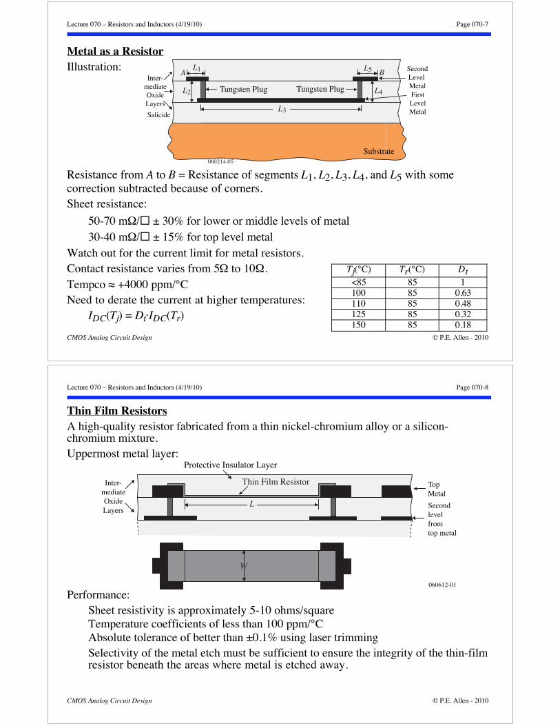
Polysilicon Resistor
30-100 ohms/square (unshielded)100-500 ohms/square (shielded)Absolute accuracy = ±3 0%Relative accuracy = 2% (5 μm)Temperature coefficient = 500-1000 ppm/°CVoltage coefficient 100 ppm/VComments:• Used for fuzzes and laser trimming• Good general resistor with low parasitics
Lecture 070 – Resistors and Inductors (4/19/10) Page 070-6
CMOS Analog Circuit Design © P.E. Allen - 2010
N-well Resistor
p- substrate
FOX FOX
Metal
n- well
n+
FOX
n-well
n+ n+
L
TungstenPlug
IntermediateOxide Layer
TungstenPlug
First Level Metal
STI STI
p-substrate
L
060214-04 LOCOS Technology
1000-5000 ohms/squareAbsolute accuracy = ±40%Relative accuracy 5%Temperature coefficient = 4000 ppm/°CVoltage coefficient is large 8000 ppm/VComments:• Good when large values of resistance are needed.• Parasitics are large and resistance is voltage dependent• Could put a p+ diffusion into the well to form a pinched resistor
Lecture 070 – Resistors and Inductors (4/19/10) Page 070-7
CMOS Analog Circuit Design © P.E. Allen - 2010
Metal as a ResistorIllustration:
Resistance from A to B = Resistance of segments L1, L2, L3, L4, and L5 with somecorrection subtracted because of corners.Sheet resistance:
50-70 m / ± 30% for lower or middle levels of metal30-40 m / ± 15% for top level metal
Watch out for the current limit for metal resistors.Contact resistance varies from 5 to 10 .Tempco +4000 ppm/°CNeed to derate the current at higher temperatures:
IDC(Tj) = Dt·IDC(Tr)
Salicide
FirstLevelMetal
SecondLevel Metal
Inter-mediateOxideLayers
Tungsten Plug
Substrate
Tungsten Plug
A BL1
L2
L3
L4
L5
060214-05
Tj(°C) Tr(°C) Dt<85 85 1100 85 0.63110 85 0.48125 85 0.32150 85 0.18
Lecture 070 – Resistors and Inductors (4/19/10) Page 070-8
CMOS Analog Circuit Design © P.E. Allen - 2010
Thin Film ResistorsA high-quality resistor fabricated from a thin nickel-chromium alloy or a silicon-chromium mixture.Uppermost metal layer:
060612-01
Secondlevel fromtop metal
Inter-mediateOxideLayers
Top Metal
Protective Insulator Layer
Thin Film Resistor
L
W
Performance:Sheet resistivity is approximately 5-10 ohms/squareTemperature coefficients of less than 100 ppm/°CAbsolute tolerance of better than ±0.1% using laser trimmingSelectivity of the metal etch must be sufficient to ensure the integrity of the thin-filmresistor beneath the areas where metal is etched away.
Lecture 070 – Resistors and Inductors (4/19/10) Page 070-9
CMOS Analog Circuit Design © P.E. Allen - 2010
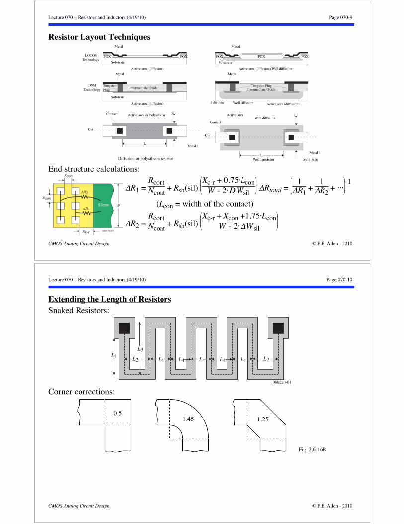
Resistor Layout Techniques
060219-01
Metal 1
Active area or PolysiliconContact
Diffusion or polysilicon resistor
L
W
Metal 1
Well diffusionContact
Well resistorL
WActive area
FOX FOXFOX
Metal
Active area (diffusion)
FOX FOX
Metal
Active area (diffusion) Well diffusion
Cut
Cut
Substrate Substrate
Metal
Active area (diffusion)
Substrate
TungstenPlug
LOCOSTechnology
DSMTechnology
Metal
Active area (diffusion)
Substrate
Tungsten Plug
Well diffusionSubstrate
Intermediate Oxide Intermediate Oxide
End structure calculations:
R1 = RcontNcont
+ Rsh(sil) Xc-r + 0.75·Lcon
W - 2·DWsil Rtotal =
1R1
+1R2
+ ···-1
(Lcon = width of the contact)
R2 = RcontNcont
+ Rsh(sil) Xc-r + Xcon +1.75·Lcon
W - 2· Wsil
Lecture 070 – Resistors and Inductors (4/19/10) Page 070-10
CMOS Analog Circuit Design © P.E. Allen - 2010
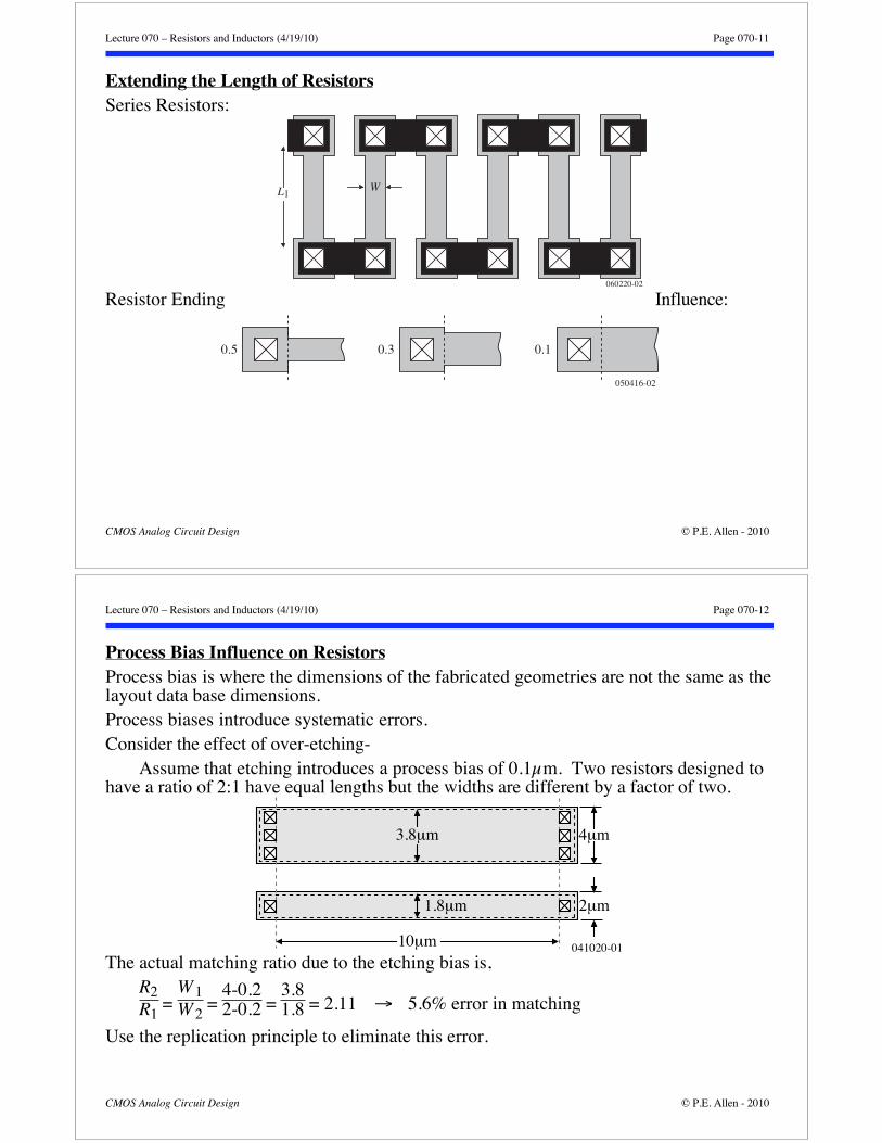
Extending the Length of ResistorsSnaked Resistors:
060220-01
L1 L2 L2L4 L4
L3
L4 L4 L4
Corner corrections:
0.51.45 1.25
Fig. 2.6-16B
Lecture 070 – Resistors and Inductors (4/19/10) Page 070-11
CMOS Analog Circuit Design © P.E. Allen - 2010
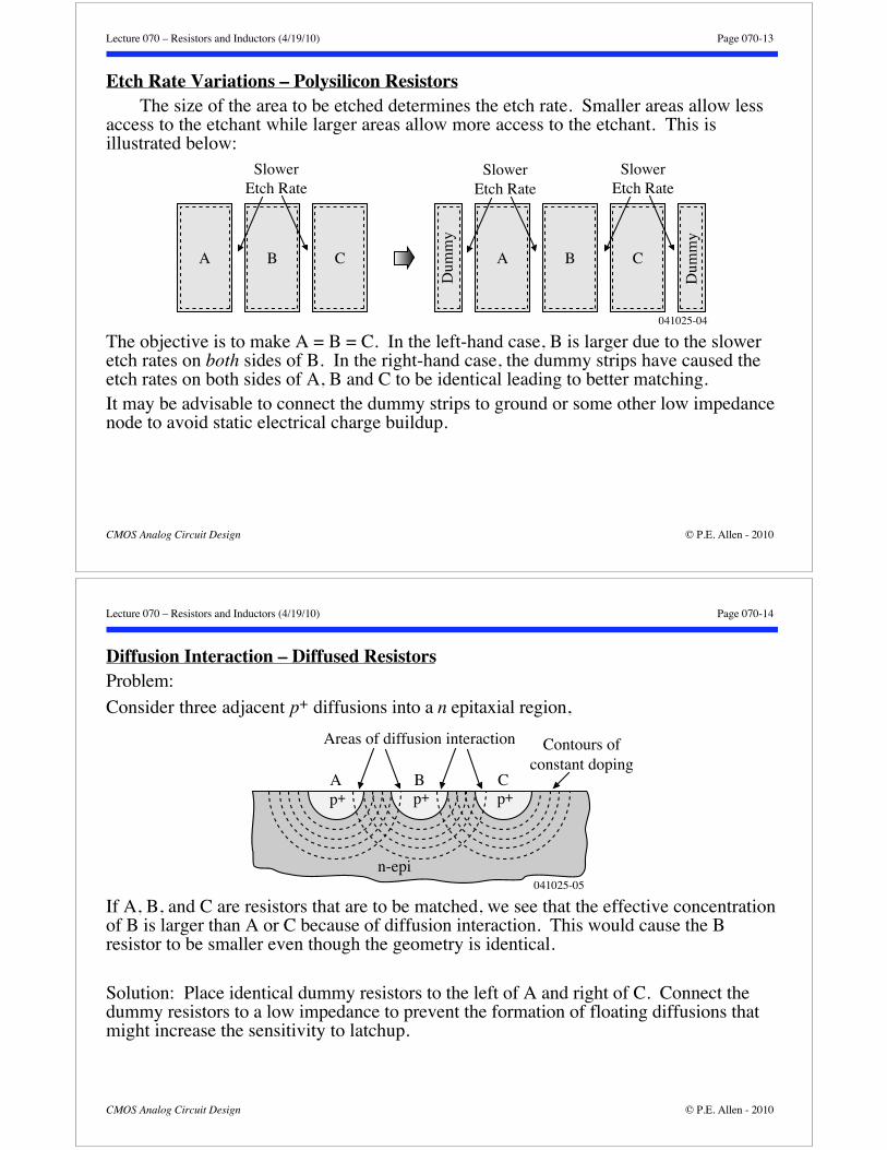
Extending the Length of ResistorsSeries Resistors:
Resistor Ending Influence:
050416-02
0.5 0.3 0.1
060220-02
L1W
Lecture 070 – Resistors and Inductors (4/19/10) Page 070-12
CMOS Analog Circuit Design © P.E. Allen - 2010
Process Bias Influence on ResistorsProcess bias is where the dimensions of the fabricated geometries are not the same as thelayout data base dimensions.Process biases introduce systematic errors.Consider the effect of over-etching-
Assume that etching introduces a process bias of 0.1μm. Two resistors designed tohave a ratio of 2:1 have equal lengths but the widths are different by a factor of two.
4μm
2μm
3.8μm
1.8μm
10μm 041020-01
The actual matching ratio due to the etching bias is,R2R1
= W 1W 2
= 4-0.22-0.2 =
3.81.8 = 2.11 5.6% error in matching
Use the replication principle to eliminate this error.
Lecture 070 – Resistors and Inductors (4/19/10) Page 070-13
CMOS Analog Circuit Design © P.E. Allen - 2010
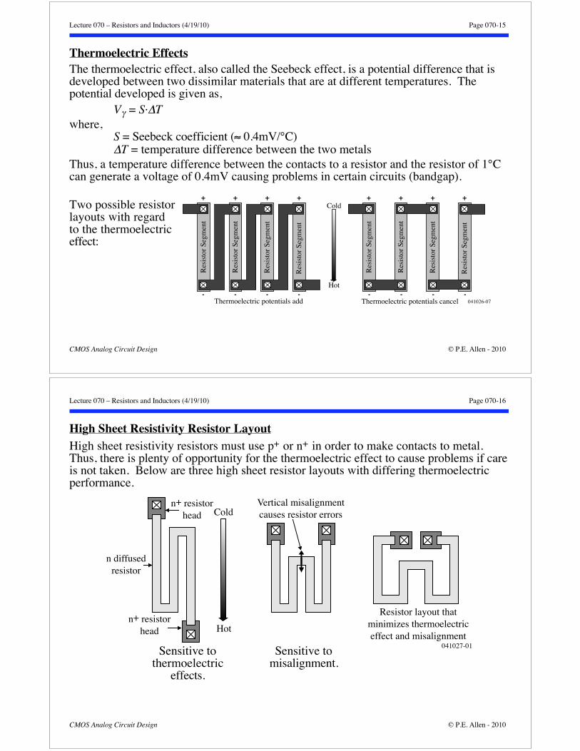
Etch Rate Variations – Polysilicon ResistorsThe size of the area to be etched determines the etch rate. Smaller areas allow less
access to the etchant while larger areas allow more access to the etchant. This isillustrated below:
A B C A B C
Dum
my
Dum
my
SlowerEtch Rate
SlowerEtch Rate
SlowerEtch Rate
041025-04
The objective is to make A = B = C. In the left-hand case, B is larger due to the sloweretch rates on both sides of B. In the right-hand case, the dummy strips have caused theetch rates on both sides of A, B and C to be identical leading to better matching.It may be advisable to connect the dummy strips to ground or some other low impedancenode to avoid static electrical charge buildup.
Lecture 070 – Resistors and Inductors (4/19/10) Page 070-14
CMOS Analog Circuit Design © P.E. Allen - 2010
Diffusion Interaction – Diffused ResistorsProblem:
Consider three adjacent p+ diffusions into a n epitaxial region,
n-epi
p+ p+ p+A B C
041025-05
Contours ofconstant doping
Areas of diffusion interaction
If A, B, and C are resistors that are to be matched, we see that the effective concentrationof B is larger than A or C because of diffusion interaction. This would cause the Bresistor to be smaller even though the geometry is identical.
Solution: Place identical dummy resistors to the left of A and right of C. Connect thedummy resistors to a low impedance to prevent the formation of floating diffusions thatmight increase the sensitivity to latchup.
Lecture 070 – Resistors and Inductors (4/19/10) Page 070-15
CMOS Analog Circuit Design © P.E. Allen - 2010
Thermoelectric EffectsThe thermoelectric effect, also called the Seebeck effect, is a potential difference that isdeveloped between two dissimilar materials that are at different temperatures. Thepotential developed is given as,
V = S· Twhere,
S = Seebeck coefficient ( 0.4mV/°C)T = temperature difference between the two metals
Thus, a temperature difference between the contacts to a resistor and the resistor of 1°Ccan generate a voltage of 0.4mV causing problems in certain circuits (bandgap).
Two possible resistorlayouts with regardto the thermoelectriceffect:
+ +
- -
Cold
Hot
Thermoelectric potentials add Thermoelectric potentials cancel
+
-
+
-
Res
isto
r Se
gmen
t
Res
isto
r Se
gmen
t
Res
isto
r Se
gmen
t
Res
isto
r Se
gmen
t
+ + + +
Res
isto
r Se
gmen
t
Res
isto
r Se
gmen
t
Res
isto
r Se
gmen
t
Res
isto
r Se
gmen
t
041026-07- - - -
Lecture 070 – Resistors and Inductors (4/19/10) Page 070-16
CMOS Analog Circuit Design © P.E. Allen - 2010
High Sheet Resistivity Resistor LayoutHigh sheet resistivity resistors must use p+ or n+ in order to make contacts to metal.Thus, there is plenty of opportunity for the thermoelectric effect to cause problems if careis not taken. Below are three high sheet resistor layouts with differing thermoelectricperformance.
n diffusedresistor
n+ resistorhead
n+ resistorhead
Cold
Hot
Vertical misalignmentcauses resistor errors
Resistor layout thatminimizes thermoelectric effect and misalignment
041027-01Sensitive tothermoelectric
effects.
Sensitive tomisalignment.
Lecture 070 – Resistors and Inductors (4/19/10) Page 070-17
CMOS Analog Circuit Design © P.E. Allen - 2010
Future Technology Impact on ResistorsWhat will be the impact of scaling down in CMOS technology?• If the size of the resistor remains the same, there will be little impact.• If the size scales with the technology, the contacts and connections to the resistors will
have more influence on the resistor.
Lecture 070 – Resistors and Inductors (4/19/10) Page 070-18
CMOS Analog Circuit Design © P.E. Allen - 2010
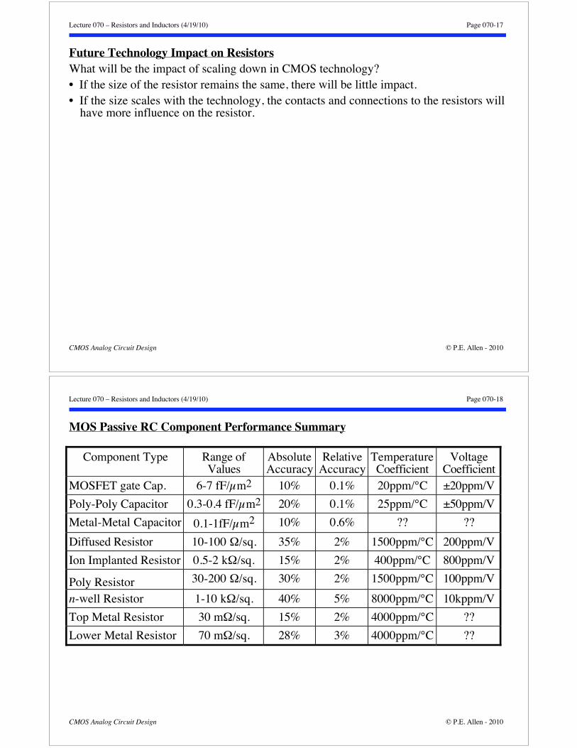
MOS Passive RC Component Performance Summary
Component Type Range ofValues
AbsoluteAccuracy
RelativeAccuracy
TemperatureCoefficient
VoltageCoefficient
MOSFET gate Cap. 6-7 fF/μm2 10% 0.1% 20ppm/°C ±20ppm/V
Poly-Poly Capacitor 0.3-0.4 fF/μm2 20% 0.1% 25ppm/°C ±50ppm/V
Metal-Metal Capacitor 0.1-1fF/μm2 10% 0.6% ?? ??
Diffused Resistor 10-100 /sq. 35% 2% 1500ppm/°C 200ppm/V
Ion Implanted Resistor 0.5-2 k /sq. 15% 2% 400ppm/°C 800ppm/V
Poly Resistor 30-200 /sq. 30% 2% 1500ppm/°C 100ppm/V
n-well Resistor 1-10 k /sq. 40% 5% 8000ppm/°C 10kppm/V
Top Metal Resistor 30 m /sq. 15% 2% 4000ppm/°C ??
Lower Metal Resistor 70 m /sq. 28% 3% 4000ppm/°C ??
Lecture 070 – Resistors and Inductors (4/19/10) Page 070-19
CMOS Analog Circuit Design © P.E. Allen - 2010
INDUCTORSCharacterization of Inductors1.) Value of the inductor
Spiral inductor†:
L μ0n2r = 4 x10⁻⁷n2r 1.2x10⁻⁶n2r
2.) Quality factor, Q = L
R
3.) Self-resonant frequency: fself = 1LC
† H.M Greenhouse, “Design of Planar Rectangular Microelectronic Inductors,” IEEE Trans. Parts, Hybrids, and Packaging, vol. 10, no. 2, June 1974,
pp. 101-109.
060216-02
2r
n = 3
Lecture 070 – Resistors and Inductors (4/19/10) Page 070-20
CMOS Analog Circuit Design © P.E. Allen - 2010
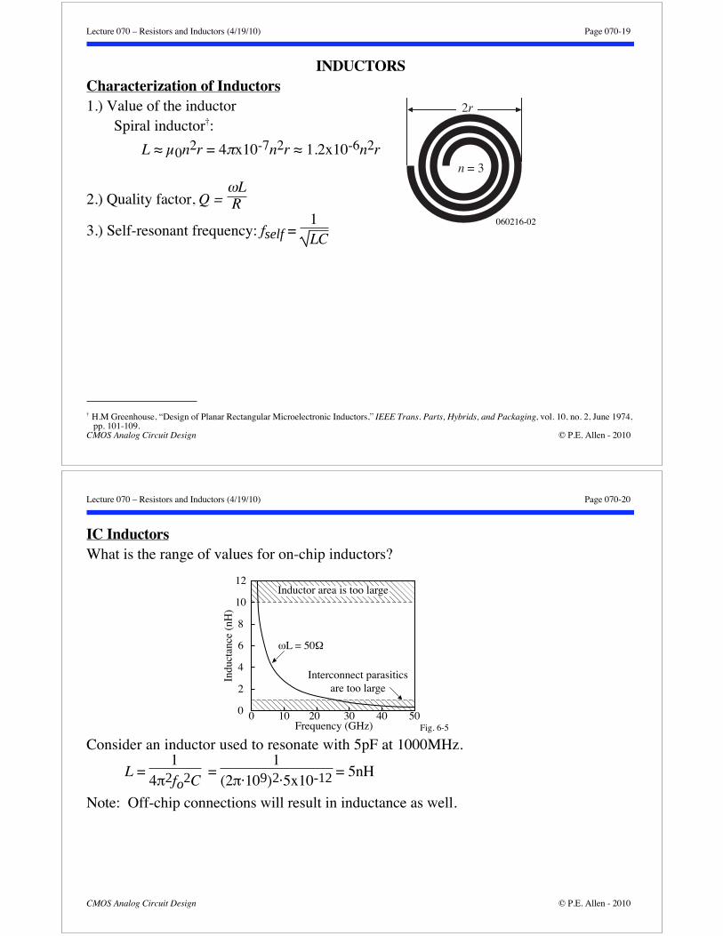
IC InductorsWhat is the range of values for on-chip inductors?
������
������
0 10 20 30 40 50
12
10
8
6
4
2
0Frequency (GHz)
Indu
ctan
ce (
nH)
ωL = 50Ω
Inductor area is too large
Interconnect parasiticsare too large
Fig. 6-5
Consider an inductor used to resonate with 5pF at 1000MHz.
L = 1
4 2fo2C =
1(2 ·109)2·5x10-12
= 5nH
Note: Off-chip connections will result in inductance as well.
Lecture 070 – Resistors and Inductors (4/19/10) Page 070-21
CMOS Analog Circuit Design © P.E. Allen - 2010
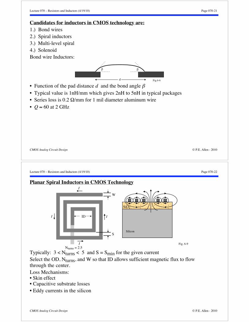
Candidates for inductors in CMOS technology are:1.) Bond wires2.) Spiral inductors3.) Multi-level spiral4.) SolenoidBond wire Inductors:
β β
d Fig.6-6
• Function of the pad distance d and the bond angle • Typical value is 1nH/mm which gives 2nH to 5nH in typical packages• Series loss is 0.2 /mm for 1 mil diameter aluminum wire• Q 60 at 2 GHz
Lecture 070 – Resistors and Inductors (4/19/10) Page 070-22
CMOS Analog Circuit Design © P.E. Allen - 2010
Planar Spiral Inductors in CMOS TechnologyI
I
I
I
W
S
ID
Nturns = 2.5
�����SiO2
Silicon
Fig. 6-9
Typically: 3 < Nturns < 5 and S = Smin for the given currentSelect the OD, Nturns, and W so that ID allows sufficient magnetic flux to flowthrough the center.Loss Mechanisms:• Skin effect• Capacitive substrate losses• Eddy currents in the silicon
Lecture 070 – Resistors and Inductors (4/19/10) Page 070-23
CMOS Analog Circuit Design © P.E. Allen - 2010
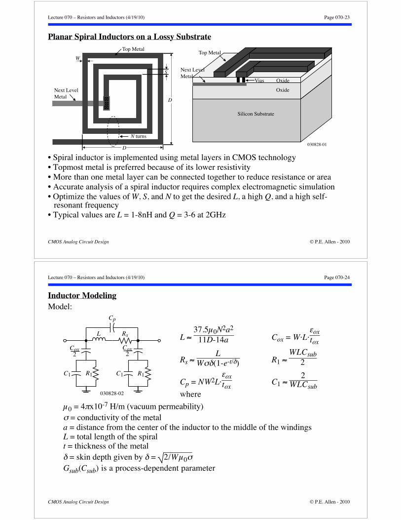
Planar Spiral Inductors on a Lossy Substrate
W
S
D
D
Top Metal
Next LevelMetal
Top Metal
Next LevelMetal
Vias
Oxide
Oxide
Silicon Substrate
N turns
030828-01
• Spiral inductor is implemented using metal layers in CMOS technology• Topmost metal is preferred because of its lower resistivity• More than one metal layer can be connected together to reduce resistance or area• Accurate analysis of a spiral inductor requires complex electromagnetic simulation• Optimize the values of W, S, and N to get the desired L, a high Q, and a high self-
resonant frequency• Typical values are L = 1-8nH and Q = 3-6 at 2GHz
Lecture 070 – Resistors and Inductors (4/19/10) Page 070-24
CMOS Analog Circuit Design © P.E. Allen - 2010
Inductor ModelingModel:
L 37.5μ0N2a2
11D-14a Cox = W·L·ox
tox
Rs L
W (1-e-t/ ) R1 WLCsub
2
Cp = NW2L·ox
tox C1
2WLCsub
where
μ0 = 4 x10⁻⁷ H/m (vacuum permeability) = conductivity of the metal
a = distance from the center of the inductor to the middle of the windingsL = total length of the spiralt = thickness of the metal = skin depth given by = 2/Wμ0
Gsub(Csub) is a process-dependent parameter
Cp
L Rs
Cox2
Cox2
C1 C1R1 R1
030828-02
Lecture 070 – Resistors and Inductors (4/19/10) Page 070-25
CMOS Analog Circuit Design © P.E. Allen - 2010
Inductor Modeling – ContinuedDefinition of the previous components:
Rs is the low frequency resistive loss of a metal and the skin effectCp arises from the overlap of the cross-under with the rest of the spiral. The lateralcapacitance from turn-to-turn is also included.Cox is the capacitance between the spiral and the substrateR1 is the substrate loss due to eddy currentsC1 is capacitance of the substrate
Design specifications:L = desired inductance valueQ = quality factorfSR = self-resonant frequency. The resonant frequency of the LC tank represents theupper useful frequency limit of the inductor. Inductor operation frequency should belower than fSR, f < fSR.
ASITIC: A software tool for analysis and simulation of CMOS spiral inductors andtransformers.
http://formosa.eecs.berkeley.edu/~niknejad/asitic.html
Lecture 070 – Resistors and Inductors (4/19/10) Page 070-26
CMOS Analog Circuit Design © P.E. Allen - 2010
Guidelines for Designing CMOS Sprial Inductors†
D – Outer diameter:• As D increases, Q increases but the self-resonant frequency decreases• A good design generally has D < 200μm
W – Metal width:• Metal width should be as wide as possible• As W increases, Q increases and Rs decreases• However, as W becomes large, the skin effects are more significant, increasing Rs• A good value of W is 10μm < W < 20μm
S – Spacing between turns:• The spacing should be as small as possible• As S and L increase, the mutual inductance, M, decreases• Use minimum metal spacing allowed in the technology but make sure the inter-winding capacitance between turns is not significant
N – Number of turns:
† Jaime Aguilera, et. al., “A Guide for On-Chip Inductor Design in a Conventional CMOS Process for RF Applications,” Applied Microwave &
Wireless, pp. 56-65, Oct. 2001.
• Use a value that gives a layout convenient to work with other parts of the circuit
Lecture 070 – Resistors and Inductors (4/19/10) Page 070-27
CMOS Analog Circuit Design © P.E. Allen - 2010
Design ExampleA 2GHz LC tank is to be designed as a part of LC oscillator. The C value is given as 3pF.(a) Find value of L. (b) Design a spiral inductor with L value (± 5% range) from (a) usingASITIC. Optimize design parameters, W, S, D and N to get a high Q (Qmin = 5). Show L,Q, fSR value obtained from simulation. (c) Show the layout. (d) Give a lumped circuitmodel.Solution(a) LC tank oscillation frequency is given as 2GHz.
osc =1
LC , L =1
osc2 C
=1
(2 2 109 )2 (3 10-12)= 2.11 10-9
L = 2.11nH is desired.(b) L = 2.11nH(± 5%) is used as input parameter. Several design parameters are triedto get high Q and fSR values. Final design has
• Parameters: W = 19um, S = 1um, D = 200um, N = 3.5• Resulting inductor: L = 2.06nH, Q = 7.11, fSR = 9.99GHz @ 2GHz
This design is acceptable as Q > Qmin and f < fSR .
Lecture 070 – Resistors and Inductors (4/19/10) Page 070-28
CMOS Analog Circuit Design © P.E. Allen - 2010
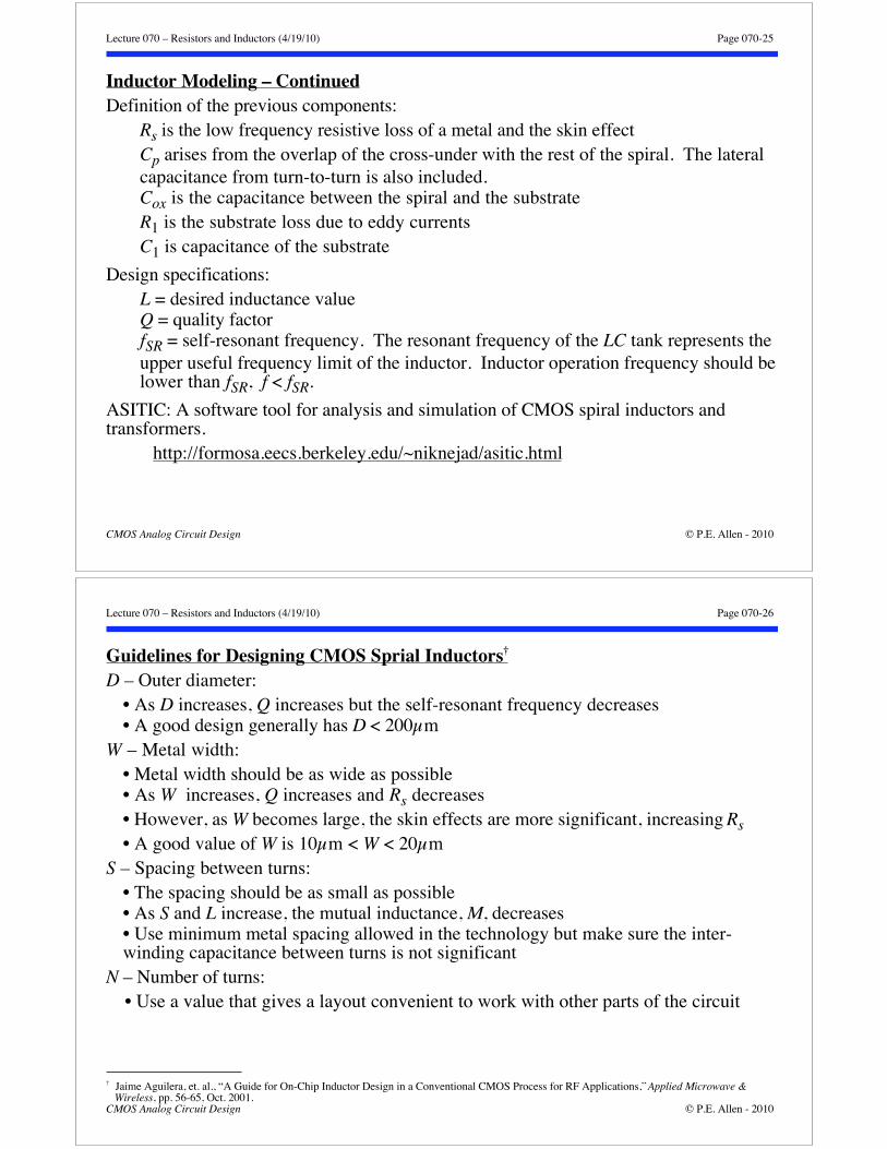
Design Example-Continued(c.) ASITIC generates a layout automatically. It can besaved and imported to use in other tools such as Cadence,ADS and Sonnet.
(d) Analysis in ASITIC gives the following model.2.06nH 3.5
123fF 128fF
4.51-3
The model is usually not symmetrical and this can be used for differential configurationwhere none of the two ports are ac-grounded.
Lecture 070 – Resistors and Inductors (4/19/10) Page 070-29
CMOS Analog Circuit Design © P.E. Allen - 2010
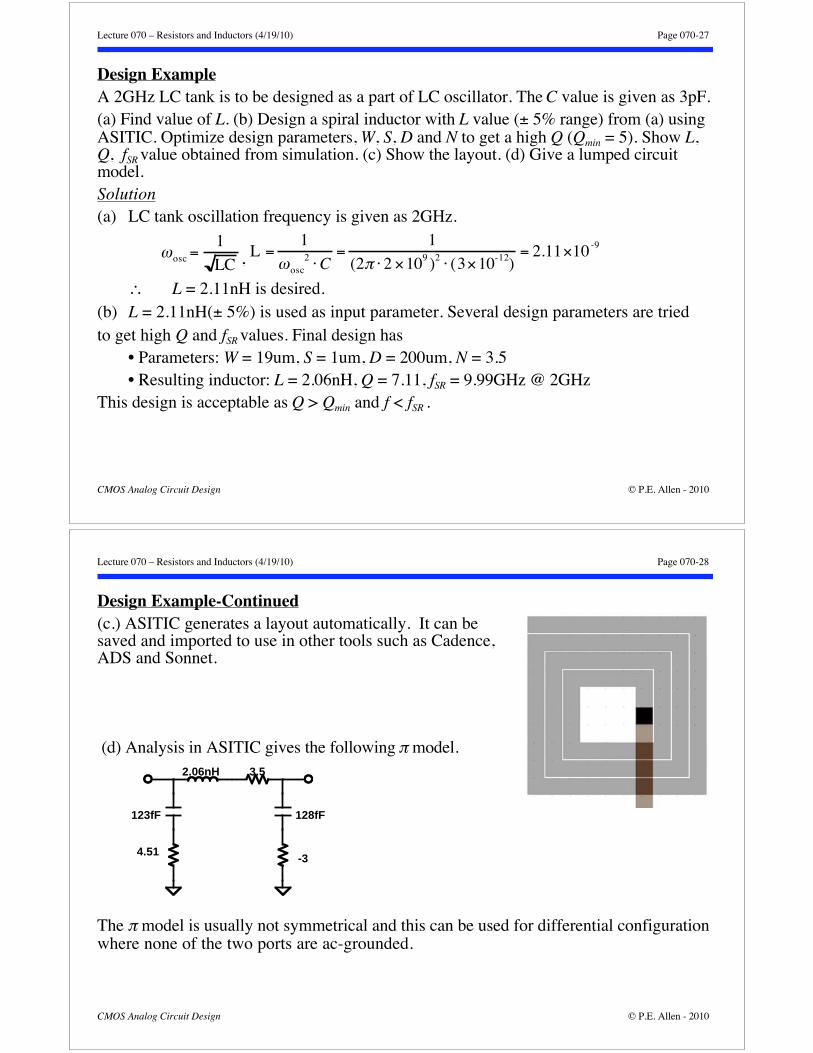
Reduction of Capacitance to GroundComments concerning implementation:1.) Put a metal ground shield between the inductor and the silicon to reduce the
capacitance.• Should be patterned so flux goes through but electric field is grounded• Metal strips should be orthogonal to the spiral to avoid induced loop current• The resistance of the shield should be low to terminate the electric field
2.) Avoid contact resistance wherever possibleto keep the series resistance low.
3.) Use the metal with the lowest resistanceand farthest away from the substrate.
4.) Parallel metal strips if other metal levelsare available to reduce the resistance.
Example
Fig. 2.5-12
Lecture 070 – Resistors and Inductors (4/19/10) Page 070-30
CMOS Analog Circuit Design © P.E. Allen - 2010
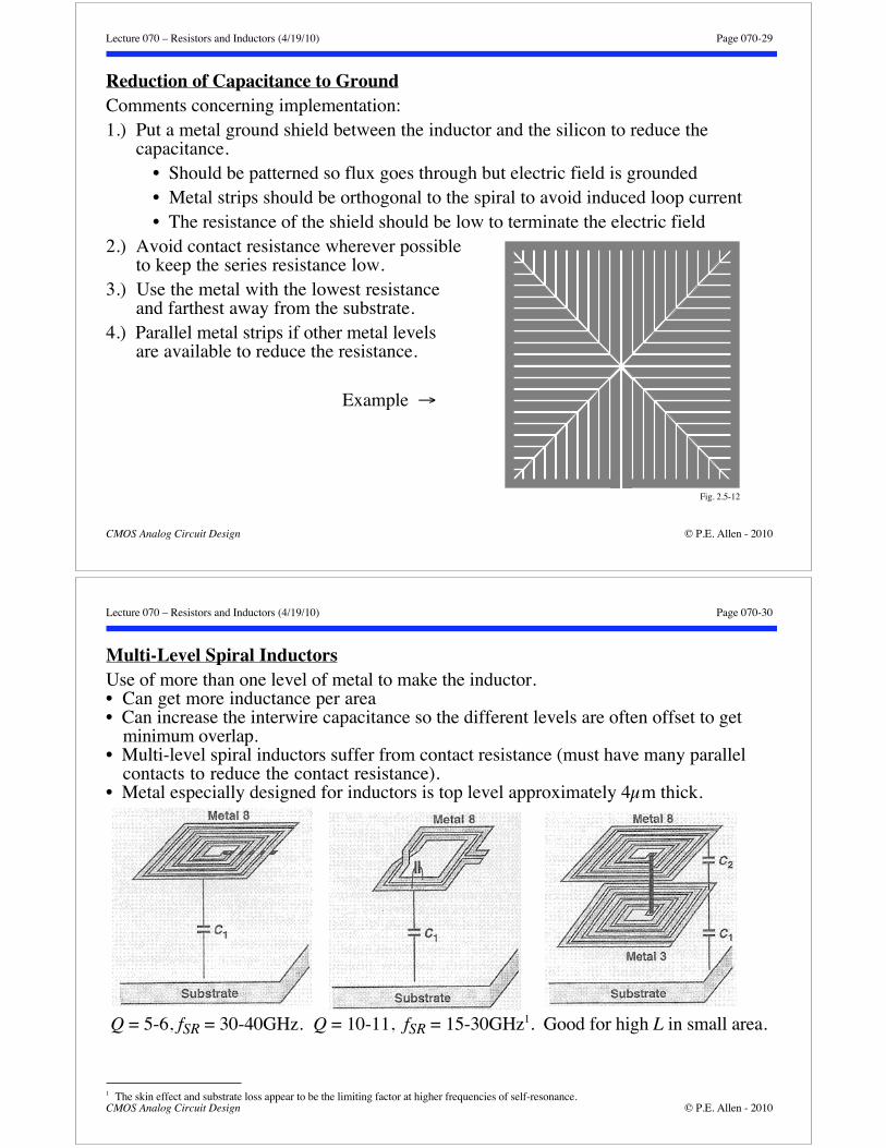
Multi-Level Spiral InductorsUse of more than one level of metal to make the inductor.• Can get more inductance per area• Can increase the interwire capacitance so the different levels are often offset to get
minimum overlap.• Multi-level spiral inductors suffer from contact resistance (must have many parallel
contacts to reduce the contact resistance).• Metal especially designed for inductors is top level approximately 4μm thick.
Q = 5-6, fSR = 30-40GHz. Q = 10-11, fSR = 15-30GHz1. Good for high L in small area.
1 The skin effect and substrate loss appear to be the limiting factor at higher frequencies of self-resonance.
Lecture 070 – Resistors and Inductors (4/19/10) Page 070-31
CMOS Analog Circuit Design © P.E. Allen - 2010
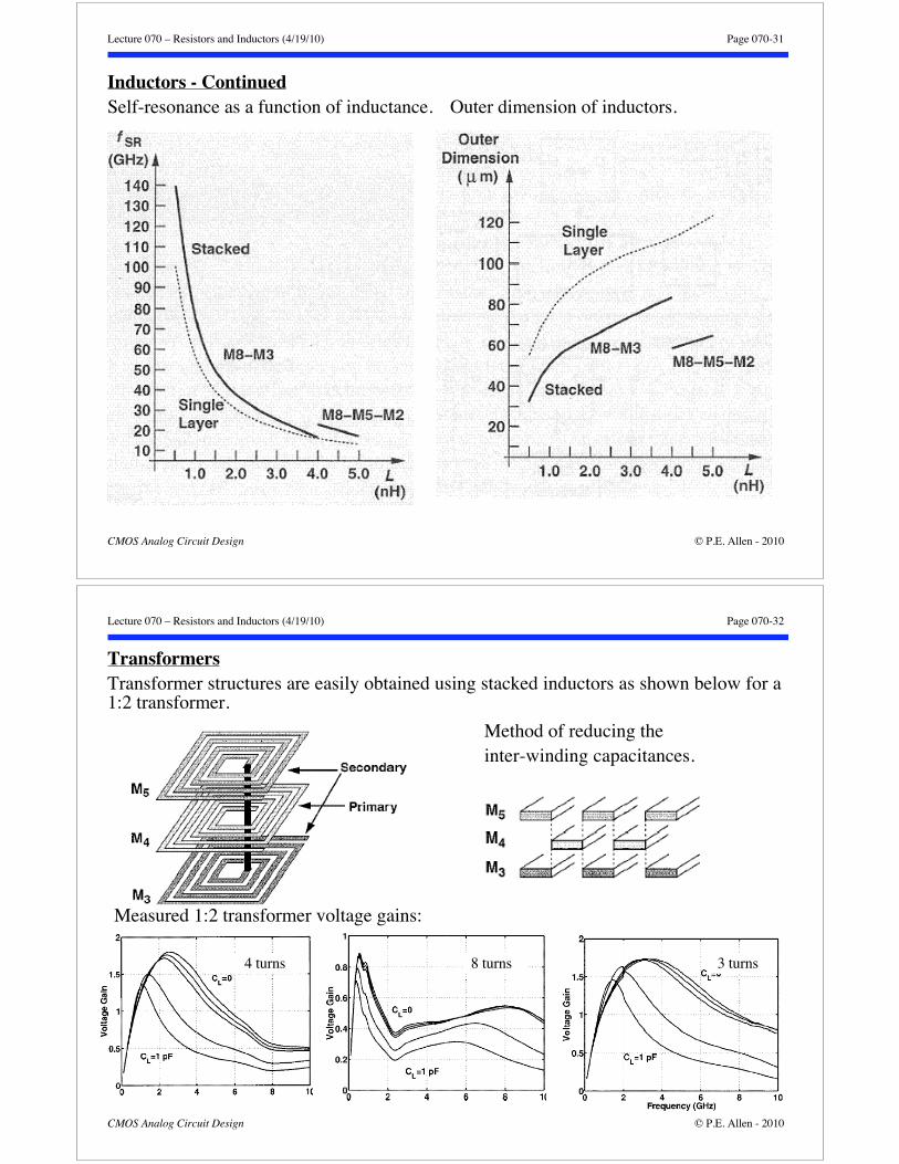
Inductors - ContinuedSelf-resonance as a function of inductance. Outer dimension of inductors.
Lecture 070 – Resistors and Inductors (4/19/10) Page 070-32
CMOS Analog Circuit Design © P.E. Allen - 2010
TransformersTransformer structures are easily obtained using stacked inductors as shown below for a1:2 transformer.
Method of reducing theinter-winding capacitances.
4 turns 8 turns 3 turns
Measured 1:2 transformer voltage gains:
Lecture 070 – Resistors and Inductors (4/19/10) Page 070-33
CMOS Analog Circuit Design © P.E. Allen - 2010
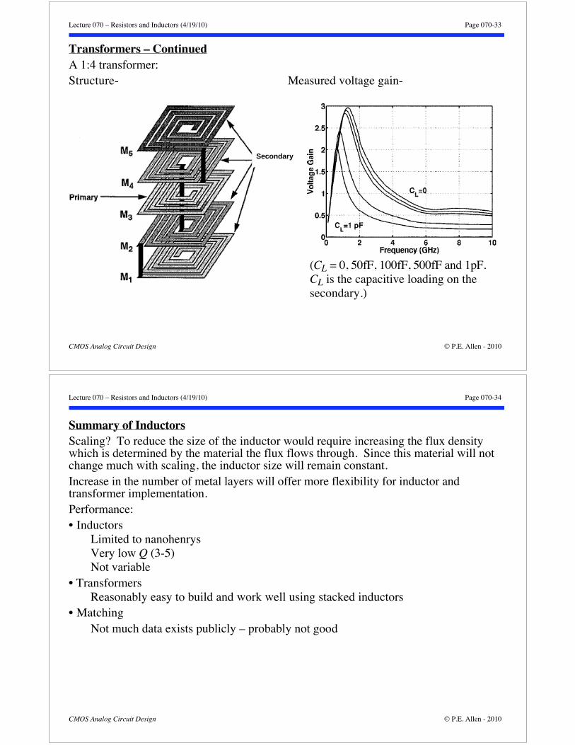
Transformers – ContinuedA 1:4 transformer:Structure- Measured voltage gain-
(CL = 0, 50fF, 100fF, 500fF and 1pF.CL is the capacitive loading on thesecondary.)
Secondary
Lecture 070 – Resistors and Inductors (4/19/10) Page 070-34
CMOS Analog Circuit Design © P.E. Allen - 2010
Summary of InductorsScaling? To reduce the size of the inductor would require increasing the flux densitywhich is determined by the material the flux flows through. Since this material will notchange much with scaling, the inductor size will remain constant.Increase in the number of metal layers will offer more flexibility for inductor andtransformer implementation.Performance:• Inductors
Limited to nanohenrysVery low Q (3-5)Not variable
• TransformersReasonably easy to build and work well using stacked inductors
• MatchingNot much data exists publicly – probably not good
Lecture 070 – Resistors and Inductors (4/19/10) Page 070-35
CMOS Analog Circuit Design © P.E. Allen - 2010
SUMMARY• Types of resistors include diffused, well, polysilicon and metal• Resistors are characterized by:
- Value- Linearity- Power- Parasitics
• Technology effects on resistors includes:- Process bias- Diffusion interaction- Thermoelectric effects- Piezoresistive effects
• Inductors are made by horizontal metal spirals, typically in top metal• Inductors are characterized by:
- Value- Losses- Self-resonant frequency- Parasitics
• RF transformers are reasonably easy to build and work well using stacked inductors