layered arsenic-doped black phosphorus electronic supplementary information for raman ... ·...
TRANSCRIPT

Electronic Supplementary Information for
Raman and Electrical Transport Properties of Few-Layered Arsenic-Doped Black Phosphorus
Nihar R Pradhana,b*, C. Garciab,c, Michael C. Luckingd, Srimanta Pakhirab,e,f,g, Juan Martinezb,c, Daniel Rosenmannh, Ralu Divanh, Anirudha V. Sumanth, Humberto
Terronesd, Jose L. Mendoza- Cortesb,c,g, Stephen A. McGillb, Nikolai D. Zhigadloi,j, Luis Balicasb,c*
Department of Chemistry, Physics and Atmospheric Sciences, Jackson State University, Jackson, MS 39217, USA.bNational High Magnetic Field Laboratory, Florida State University, Tallahassee, FL 32310, USA.c Department of Physics, College of Arts and Sciences, Florida State University, Tallahassee, Florida, 32306, USA.dDepartment of Physics, Applied Physics and Astronomy, Rensselaer Polytechnic Institute, Troy, New York 12180, United States.eDiscipline of Physics and Metallurgy Engineering & Materials Science, Indian Institute of Technology Indore (IITI), Simrol, Khandwa Road, Indore, 453552, MP, India.fDepartment of Chemical & Biomedical Engineering, FAMU-FSU College of Engineering, Florida State University, Tallahassee, Florida, 32310, USA.gDepartment of Scientific Computing, Materials Science and Engineering, High Performance Materials Institute, Florida State University, Tallahassee, Florida, 32304, USA.hCenter for Nanoscale Materials, Argonne National Laboratory, 9700 S-Cass Avenue, Argonne, IL-60439, USAiDepartment of Chemistry and Biochemistry, University of Bern, Freiestrasse 3, CH-3012 Bern, Switzerland.jCrystMat Company, CH-8046 Zurich, Switzerland
1. Synthesis and X-ray crystallography:
Single crystals of As-bP were grown through the cubic-anvil high-pressure and high-
temperature technique. Pellets containing the high purity powders of grey arsenic
(99.9999 %) and red phosphorus (99.999 %) with molar ratio 30:70 were enclosed in a
boron nitride container and placed into a graphite heater. A pressure of 10 kbar was
applied at room temperature. Then, by keeping pressure constant the temperature was
ramped up to 1050 C in 3 h, maintained there for 3 h, and after that cooled to 650 C in
15 h, and finally abruptly quenched to room temperature. Once the pressure was released,
the sample was removed. More details about high-pressure instrumentation are given
elsewhere Ref S1, S2. The structural characterization was performed by means of
Electronic Supplementary Material (ESI) for Nanoscale.This journal is © The Royal Society of Chemistry 2019

standard single crystal X-ray diffraction measurements performed at room temperature,
which confirmed the single-phase nature of the crystals. At high pressure conditions, As-
bP crystallizes in orthorhombic structure with the space group of Cmca and the lattice
parameters are a = 3.388(2) Å, b = 10.566(9) Å, and c = 4.390(3) Å. Energy-dispersive x-
ray (EDX) spectroscopy was used to analyze the chemical composition of the grown
crystals. The EDX analysis performed on several crystals correspond to the As0.25bP0.75
chemical composition, see Fig. S2.
Figure S1: Powder X-ray diffraction pattern of a ground b-As0.25P075 single crystal as a function of
diffraction angle. It reveals not clear evidence for impurity phases.

Table S1. Crystallographic data and structure refinement for b-As0.25P0.75.
Identification code shelx Empirical formula As P Formula weight 167.83 Temperature 298(2) K Wavelength 0.71073 Å Crystal system Orthorhombic Space group Cmca Unit cell dimensions a = 3.388(2) Å α= 90°.
b = 10.566(9) Å β= 90°. c = 4.390(3) Å γ = 90°.
Volume 157.15(19) Å3 Z 2 Density (calculated) 3.547 mg/m3 Absorption coefficient 12.026 mm-1 F(000) 156 Crystal size 0.339 x 0.154 x 0.054 mm3 Theta range for data collection 3.857 to 31.751°. Index ranges -5<=h<=5, -15<=k<=15, -6<=l<=6 Reflections collected 1986 Independent reflections 156 [R(int) = 0.0667] Completeness to theta = 25.242° 100.0 % Absorption correction Gaussian Max. and min. transmission 0.892 and 0.09 Refinement method Full-matrix least-squares on F2 Data / restraints / parameters 156 / 0 / 7 Goodness-of-fit on F2 1.155 Final R indices [I>2sigma(I)] R1 = 0.0508, wR2 = 0.1325 R indices (all data) R1 = 0.0546, wR2 = 0.1370 Extinction coefficient n/a Largest diff. peak and hole 1.862 and -1.268 e.Å-3

2. Energy Dispersive Analysis of b-As0.25P0.75
Element
Line
Weight % Weight %
Error
Atom % Atom %
Error
P K 55.44 +/- 0.38 75.06 +/- 0.52
As K 44.56 +/- 1.00 24.94 +/- 0.56
Total 100.00 100.00
Figure S2: Electron dispersive spectroscopy analysis of a b-As0.25P0.75 single-crystal grown via the high pressure method. As seen, the material contains only As and P with table below indicating a
composition that is very close x = 0.25 in As. These values correspond to the average of the data collected from 6 points throughout the crystal whose picture is shown in the inset.
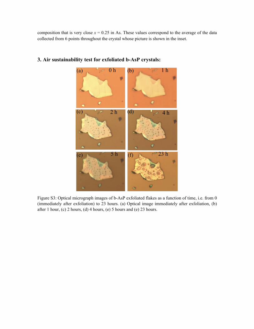
3. Air sustainability test for exfoliated b-AsP crystals:
Figure S3: Optical micrograph images of b-AsP exfoliated flakes as a function of time, i.e. from 0 (immediately after exfoliation) to 23 hours. (a) Optical image immediately after exfoliation, (b) after 1 hour, (c) 2 hours, (d) 4 hours, (e) 5 hours and (e) 23 hours.

4. Raman Spectroscopy of encapsulated b-AsP crystal with polymer:
In Figure S4 (a-c) the theoretically calculated Raman spectra (green lines) are plotted
together with the experimentally measured ones. (a), (b) and (c) correspond to 50%,
62.5% and 75%, respectively of As doped in black-phosphorus as calculated using the
DFT method. (d) Raman Spectroscopy of b-AsP crystal months after exfoliation and
encapsulation in CytopTM. The Raman spectrum is similar to the one of exfoliated flakes
presented in the main text. This confirms that the intrinsic properties of b-AsP can be
preserved for a long time in air when protected by a suitable polymer encapsulation.
Figure S4: Experimental Raman spectra with theoretically calculated ones for 50% As (a), 62.5% As (b) and 75% As (c) doped black-phosphorus. (d) Raman spectra for exfoliated b-AsP flakes, encapsulated in polymer after 6 months in a desiccator and a month under air exposure.

5. Polar plot of polarization Raman study
Figure S5: Angular dependence of the Raman intensity for each Raman mode branch at seven different frequencies. (a) Raman intensity as a function of the polarization angle for the modes at 239 cm-1 and 257.4 cm-1 associated to As-As bonds. (b) Raman intensity as a function of the polarization angle for three peaks at 316 cm-1, 346 cm-1 and 364 cm-1 resulting from the As-P bonds. (c) Raman intensity as a function of the polarization angle for the modes at 426 cm-1 and 456 cm-1 which correspond to the P-P bonds in b-AsP. Dots are the measured values and solid lines are guides to eyes.
As shown in Fig. S5, we analyzed the polarization dependence of all main Raman peaks.
All peaks from the three different Raman branches show a polarization-dependent Raman
intensity. We have measured polarization dependent Raman studies on 3 different flakes
using the same laser source and all three samples show consistent polarization-dependent
Raman intensity data. Figures S5a, S5b and S5c show the angular dependence of the
Raman intensity at 239 cm-1 and 257.4 cm-1 corresponding to As-As bonds, 316 cm-1, 346
cm-1 and 364 cm-1 and 426 cm-1 and 456 cm-1. If one compares Figs. S4 and S5 with the
Raman modes of pristine b-P in Ref. S3 (see its Fig. 3), one can see groups of modes, one
at very low frequencies, that is between 235 and 260 cm-1, another one between 300 and
400 cm-1 , and a third one between 400 and 500 cm-1. Table S2 below provides our
calculated Raman modes associated with these Raman mode groups for b-AsP. As seen,
each Raman mode involves vibrations associated to P-P, As-As, and As-P bonds.

In Fig. S5 one sees a 90o rotation between the angular dependences displayed by
the modes of the third group with respect to the groups displaying modes at lower
frequencies. B. Liu et al., (Ref. S3) attributed a similar contrasting angular dependence
observed in b-As0.87P0.13, to the distinct character of the modes, that is A1g for the lower
frequency modes, and B2g for the higher frequency ones. in. In contrast Ribeiro et al. Ref.
[S5] sees twice the periodicity for the B2g modes when compared to the A1g one. This
could be attributed to the use of polarized collection, in contrast to the use of unpolarized
collection as used by us.
Notice that the Raman mode calculations in Liu et al. (Ref. S3) includes only the
As-P bonds, and an As fraction x =0.5. In our calculations, we include all chemical bonds
and the actual As configuration for x = 0.25.
As for the contrasting angular dependence observed for the different modes we do
not have a solid explanation for it, since our calculations contrast with the previous ones
by indicating that all modes are A type. Here, we can only speculate that the As clusters
might be preferentially oriented along a certain crystallographic direction. The lower
frequency modes involve mainly As-As and As-P bonds, while the higher frequency ones
are mainly associated with the P-P bonds that do not display a similar axial asymmetry.
Perhaps this might lead to their contrasting anisotropies. Notice that higher As
concentrations should lead to As clusters of distinct sizes and geometries naturally
leading to distinct frequencies and anisotropies for their Raman modes.
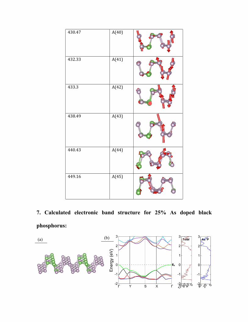
6. Table S2: Calculated Raman modes:
Table S2 shows the frequencies in the left column and middle column represents modes name with image of modes showing in right column. The unit cell of the b-As0.25P0.75 structure using P1 symmetry, we calculated 45 Raman active modes. We listed the 15 most intense modes and plot the corresponding atomic displacements in the table. Arsenic atoms are is Green and Phosphorous atoms are in purple. Since the symmetry of the primitive cell is P1, the point symmetry associated with this cell is C1. Therefore, Table S2 shows only modes belonging to one irreducible representation, i.e. “A”. This means that all the vibrational modes are Raman active and should be labeled as A.
Frequency (cm-1) Name Image

231.8 A(20)
242.46 A(21)
249.59 A(22)
259.12 A(24)
309.84 A(25)
312.45 A(26)
329.9 A(27)
384.17 A(33)
423.02 A(39)
430.47 A(40)
432.33 A(41)
433.3 A(42)
438.49 A(43)
440.43 A(44)
449.16 A(45)
7. Calculated electronic band structure for 25% As doped black
phosphorus:
(a) (b)

Figure S6: (a) Configuration of As (green atom) and P (purple atoms) that would yield the experimental Raman modes observed for b-AsxP1-x where x = 0.25 according to our DFT calculations. (b) Band structure calculations, total density of states (DOS) and p-subshells DOS of the As contributing in the total DOS using the UDFT-HSE06-D2 DFT method (or HSE06-D for short) for monolayer b-As0.25P0.75 in panel (a).
We performed electronic band structure calculations for single layer, bi-layer, tri-layer
and bulk crystals of b-As0.25 P0.75 following the particular As configuration that according
to the DFT calculations would describe the observed experimental Raman spectra. The
estimated size of the gap for monolayer, 2L, 3L and bulk are 1.558 eV, 1.123 eV, 0.84 eV
and 0.21 eV respectively. In general the band gaps are smaller than those calculated for
pristine b-P, see ref. [S4]. In this plot the bands are normalized (i.e. the Fermi energy EF
was subtracted from the each band energy) .
Table S3: Lattice constants (a, b, c), band gap and the position of Fermi energy (EF) are
reported.
Materials Symmetry(Space group
or layer group no.)
a in Å b in Å c in Å Band Gap (Eg)
in eV
Fermi Energy (EF) Level in eV
Bulk Structure Pristine bP
CMCA(64)
3.336 10.210 4.393 0.324 -2.449
Bulk Structure b-AsP
PMC21(26)
3.423 10.299 4.397 0.210 -2.620
1Layer b-AsP
P1(1)
3.400 4.548 NA 1.558 -5.336
2Layer b-AsP
P1(1)
3.398 4.506 NA 1.123 -5.303
3Layer b-AsP
P1(1)
3.398 4.486 NA 0.840 -5.272
8. Electrical transport at T = 4 K for the FET presented in main text.

0.0
0.1
0.2
0.3
0.4
0
1
2
3
4
-60 -30 0 3010-11
10-10
10-9
10-8
10-7
10-6
-60 -30 0 3010-10
10-9
10-8
10-7
10-6
10-5
T = 4 K
(d)(c)
(b)Vds = 5 mV Vds = 10 mV Vds = 15 mV
I ds (A
)2-Terminal(a)
T = 4 K
Vds = 5 mV Vds = 10 mV Vds = 15 mV
4-TerminalIds (A
)
2-Terminal
I ds (A
)
Vbg (V)
Ids (A)
Vbg (V)
4-Terminal
Figure S7. Electrical transport properties of a As0.25bP0.75 FET at T = 4K. (a) and (b) Ids as a function Vbg for Vds = 5 mV, 10 mV and 15 mV in a linear scale measured via 2-terminal and 4-terminal configurations. (c) and (d) the same data but plotted in a semi-logarithmic scale indicating ON/OFF current ratios ranging from ~104 to 105
.
9. Ids as a function of Vds at T = 2K for the As-bP FET presented in main text.
In Figure S8 we plot the low temperature Ids as a function Vds for the b-AsP device
presented in the main text. These measurements indicate that at even at low temperatures,
the Ids as a function of Vds looks ohmic like despite having a large contact resistance
between the b-AsP and the Ti metal. The current measured using the 4-terminal
configuration still is much higher than the one obtained through the 2-terminal method.

Figure S8: 2-terminal (left) and 4-terminal (right) drain-to-source current measured under several values of the applied gate voltage at a temperature T =2 K displaying nearly ohmic like behavior.
10. Ids as a function of Vbg for the b-AsP FET presented in the main text at T = 50 K and 25 K.
Figure S9 (left) and (right) displays Ids as a function of Vbg for a b-AsP FET in a semi-
logarithmic scale and for two temperatures 50 K and 25 K, respectively. The data shows
an improved ON to OFF current ratio and subthreshold voltage swing at low
temperatures compared to room temperature. This FET shows a ~105 ON/OFF current
ratio at a small applied Vds = 15 mV.
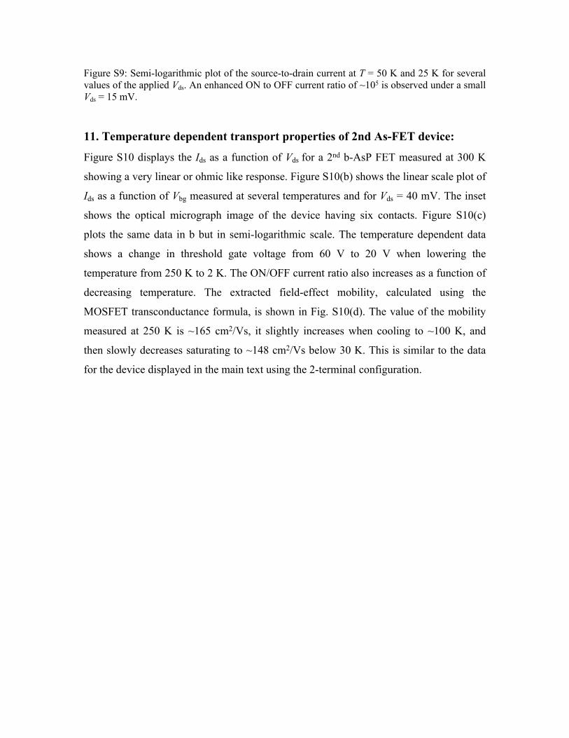
Figure S9: Semi-logarithmic plot of the source-to-drain current at T = 50 K and 25 K for several values of the applied Vds. An enhanced ON to OFF current ratio of ~105 is observed under a small Vds = 15 mV.
11. Temperature dependent transport properties of 2nd As-FET device:
Figure S10 displays the Ids as a function of Vds for a 2nd b-AsP FET measured at 300 K
showing a very linear or ohmic like response. Figure S10(b) shows the linear scale plot of
Ids as a function of Vbg measured at several temperatures and for Vds = 40 mV. The inset
shows the optical micrograph image of the device having six contacts. Figure S10(c)
plots the same data in b but in semi-logarithmic scale. The temperature dependent data
shows a change in threshold gate voltage from 60 V to 20 V when lowering the
temperature from 250 K to 2 K. The ON/OFF current ratio also increases as a function of
decreasing temperature. The extracted field-effect mobility, calculated using the
MOSFET transconductance formula, is shown in Fig. S10(d). The value of the mobility
measured at 250 K is ~165 cm2/Vs, it slightly increases when cooling to ~100 K, and
then slowly decreases saturating to ~148 cm2/Vs below 30 K. This is similar to the data
for the device displayed in the main text using the 2-terminal configuration.

Figure S10: Transport properties of a 2nd b-AsP FET. (a) Ids as a function of Vds measured at room temperature. (b) Linear scale plot of Ids as a function of Vbg under a bias voltage Vds = 40 mV and measured at several temperatures from 250 K to 2 K. Inset: optical image of the device with Ti/Au (5/80 nm) contacts. The channel length between source and drain contacts is 12.2 m and the width of the channel is 5.3 m. (c) Ids as a function Vbg in a semi-logarithmic scale. (d) The extracted mobilities from the linear fits of the traces collected at each temperature (panel (b)) as a function of the temperature.
12. Room temperature transport properties of a 3rd b-AsP-FET:
Figure S11 illustrates the p-type FET behavior of a 3rd b-AsP-FET measured at room
temperature. Figures S11(a) and S11(b) correspond to the Ids as a function of Vds
measured through 2- and 4-terminal configurations respectively, and for several values of
the applied back gate voltage (Vbg). Inset in Figure S11(a) shows the optical image of the
device with 6 deposited contacts. The FET characteristic (Ids as function of Vbg) is shown
in Figure S11(c) and S11(d) for 2- and 4-terminal measurements, respectively. The
device shows ON to OFF current ratio > 103 at 275 K.
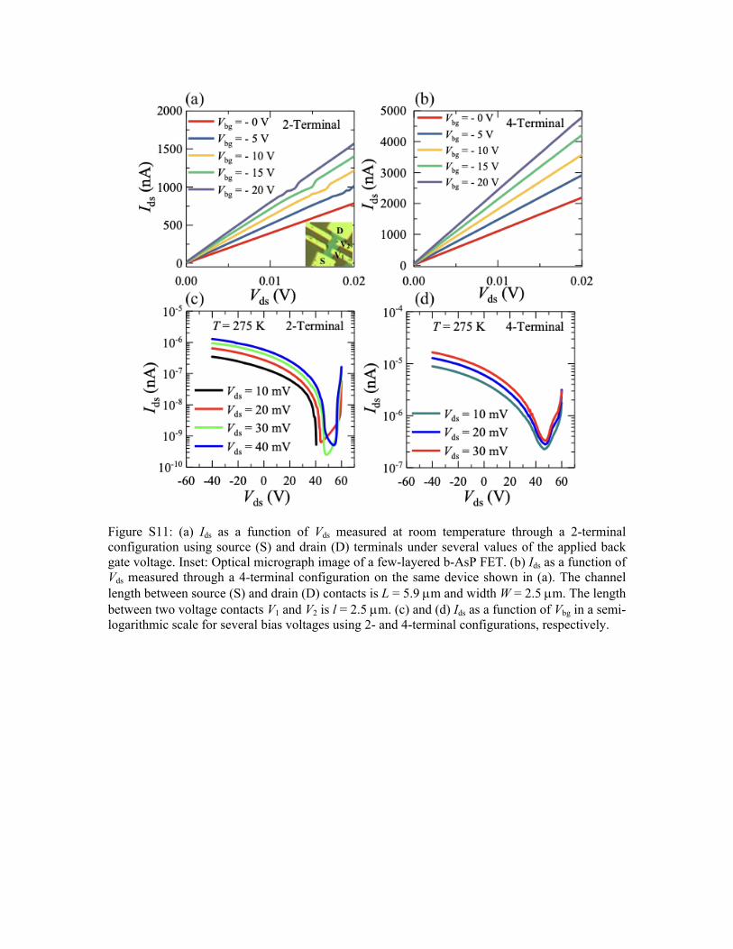
Figure S11: (a) Ids as a function of Vds measured at room temperature through a 2-terminal configuration using source (S) and drain (D) terminals under several values of the applied back gate voltage. Inset: Optical micrograph image of a few-layered b-AsP FET. (b) Ids as a function of Vds measured through a 4-terminal configuration on the same device shown in (a). The channel length between source (S) and drain (D) contacts is L = 5.9 m and width W = 2.5 m. The length between two voltage contacts V1 and V2 is l = 2.5 m. (c) and (d) Ids as a function of Vbg in a semi-logarithmic scale for several bias voltages using 2- and 4-terminal configurations, respectively.
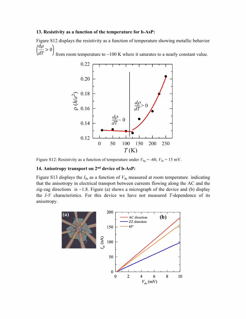
13. Resistivity as a function of the temperature for b-AsP:
Figure S12 displays the resistivity as a function of temperature showing metallic behavior
from room temperature to ~100 K where it saturates to a nearly constant value.(𝑑𝜌𝑑𝑇> 0)
Figure S12: Resistivity as a function of temperature under Vbg = -60, Vds = 15 mV.
14. Anisotropy transport on 2nd device of b-AsP:
Figure S13 displays the Ids as a function of Vds measured at room temperature indicating that the anisotropy in electrical transport between currents flowing along the AC and the zig-zag directions is ~1.8. Figure (a) shows a micrograph of the device and (b) display the I-V characteristics. For this device we have not measured T-dependence of its anisotropy.

Figure S13: b-AsP device with several anisotropy contacts using Cr/Au and Ids vs Vds graph.
REFERENCES
S1 Zhigadlo, N. D.; Weyeneth, S.; Katrych, S.; Moll, P. J. W.; Rogacki, K.; Bosma, S.; Puzniak, R.; Karpinski, J.; Batlogg B. High-pressure flux growth, structural, and superconducting properties of LnFeAsO (Ln= Pr, Nd, Sm) single crystals. Phys. Rev. B 2012, 86, 214509.
S2 Zhigadlo, N. D. High pressure crystal growth of the antiperovskite centrosymmetric superconductor SrPt3P. J. Cryst. Growth 2016, 455, 94-98.
[S3] B. Liu et al., Adv. Mater., 2015, 27, 4423-4429
[S4] Li, L.K. ; Kim, J.; Jin, C.H.; Ye, G. J.; Qiu, D. Y. ; da Jornada, F. H. ; Shi, Z. W. ; Chen, L.; Zhang, Z. C.; Yang, F. Y.; Watanabe, K. ; Taniguchi, T.; Ren, W.; Louie, S. G.; Chen, X. H.; Zhang, Y. B.; Wang, F. Direct observation of the layer-dependent electronic structure in phosphorene. Nat. Nanotechnol. 2017, 12, 21-25
[S5] Henrique B. Ribeiro, Marcos A. Pimenta, Christiano J. S. de Matos, Roberto Luiz Moreira, Aleksandr S. Rodin, Juan D. Zapata, Eunézio A. T. de Souza, Antonio H. Castro Neto, ACS Nano, 2015, 9, 4, 4270-4276