kluwer.academic.cmos.memory.circuits
TRANSCRIPT

www.dbeBooks.com - An Ebook Library

CMOS MEMORY CIRCUITS

This page intentionally left blank.
CMOS MEMORY CIRCUITS
by
Tegze P. HarasztiMicrocirc Associates
KLUWER ACADEMIC PUBLISHERS
NEW YORK, BOSTON , DORDRECHT, LONDON , MOSCOW

©2002 Kluwer Academic PublishersNew York, Boston, Dordrecht, London, Moscow
All rights reserved
No part of this eBook may be reproduced or transmitted in any form or by any means, electronic,mechanical, recording, or otherwise, without written consent from the Publisher
Created in the United States of America
Visit Kluwer Online at: http://www.kluweronline.comand Kluwer's eBookstore at: http://www.ebooks.kluweronline.com
Print ISBN 0-792-37950-0
eBook ISBN 0-306-47035-7

Contents
Preface ......................................................................................................... xi
Conventions ..................................................................................................... xvi
Chapter 1. Introduction to CMOS Memories......................................... 1
1.1 Classification and Characterization of CMOS Memories................................21.2 Random Access Memories .............................................................................10
1.2.1 Fundamentals......................................................................................101.2.2 Dynamic Random Access Memories (DRAMS) ................................. 111.2.3 Pipelining in Extended Data Output (EDO) and
Burst EDO (BEDO) DRAMS.............................................................201.2.4 Synchronous DRAMS (SDRAMs) .................................................... 251.2.5 Wide DRAMs .....................................................................................311.2.6 Video DRAMs....................................................................................331.2.7 Static Random Access Memories (SRAMs) .......................................361.2.8 Pseudo SRAMs...................................................................................401.2.9 Read Only Memories (ROMs)............................................................41
1.3 Sequential Access Memories (SAMs) ............................................................421.3.1 Principles............................................................................................421.3.2 RAM-Based SAMs.............................................................................441.3.3 Shift-Register Based SAMs................................................................451.3.4 Shuffle Memories ...............................................................................481.3.5 First-In-First-Out Memories (FIFOs) .................................................51
1.4 Content Addressable Memories (CAMS) .......................................................541.4.1 Basics .................................................................................................541.4.2 All-Parallel CAMS..............................................................................56

vi CMOS Memory Circuits
1.4.3 Word-Serial-Bit-Parallel CAMs......................................................... 581.4.4 Word-Parallel-Bit-Serial CAMs......................................................... 59
1.5 Special Memories and Combinations ............................................................. 611.5.1 Cache-Memory Fundamentals ............................................................ 611.5.2 Basic Cache Organizations ................................................................. 651.5.3 DRAM-Cache Combinations ............................................................. 701.5.4 Enhanced DRAM (EDRAM) ............................................................. 701.5.5 Cached DRAM (CDRAM) ................................................................. 721.5.6 Rambus DRAM (RDRAM) ................................................................ 731.5.7 Virtual Channel Memory (VCM) ....................................................... 76
1.6 Nonranked and Hierarchical Memory Organizations ..................................... 80
Chapter 2. Memory Cells ................................................................................... 85
2.1 Basics, Classifications and Objectives ...........................................................862.2 Dynamic One-Transistor-One-Capacitor Random Access Memory Cell....... 89
2.2.1 Dynamic Storage and Refresh ............................................................ 892.1.2 Write and Read Signals ...................................................................... 922.1.3 Design Objectives and Trade-offs ...................................................... 962.1.4 Implementation Issues ........................................................................ 97
2.1.4.1 Insulator Thickness ............................................................... 972.1.4.2 Insulator Material ................................................................. 982.1.4.3 Parasitic Capacitances ......................................................... 1032.1.4.4 Effective Capacitor Area .................................................... 105
2.3 Dynamic Three-Transistor Random Access Memory Cell ........................... 1102.3.1 Description ....................................................................................... 1102.3.2 Brief Analysis................................................................................... 111
2.4 Static 6-Transistor Random Access Memory Cell ....................................... 1132.4.1 Static Full-Complementary Storage ................................................. 1132.1.2 Write and Read Analysis ..................................................................1162.1.3 Design Objectives and Concerns ......................................................1212.1.4 Implementations ...............................................................................122
2.5 Static Four-Transistor-Two-Resistor Random AccessMemory Cells ...............................................................................................1252.5.1 Static Noncomplementary Storage ................................................ 1252.5.2 Design and Implementation ........................................................... 128
2.6 Read-Only Memory Cells ........................................................................... 1322.6.1 Read-Only Storage ........................................................................... 1322.6.2 Programming and Design ................................................................ 134
2.7 Shift-Register Cells .................................................................................. 1362.7.1 Data Shifting ....................................................................................1362.7.2 Dynamic Shift-Register Cells ........................................................... 1382.7.3 Static Shift-Register Cells ................................................................143
2.8 Content Addressable Memory Cells .............................................................1462.8.1 Associative Access ........................................................................... 1462.8.2 Circuit Implementations ................................................................... 148
2.9 Other Memory Cells .....................................................................................1512.9.1 Considerations for Uses ....................................................................1512.9.2 Tunnel-Diode Based Memory Cells ................................................. 152

Contents vii
2.9.3 Charge Coupled Device.................................................................. 1542.9.4 Multiport Memory Cells ................................................................. 1562.9.5 Derivative Memory Cells ............................................................... 158
Chapter 3. Sense Amplifiers ...............................................................163
3.1 Sense Circuits .............................................................................................1643.1.1 Data Sensing ...................................................................................1643.1.2 Operation Margins ..........................................................................1663.1.3 Terms Determining Operation Margins .......................................... 171
3.1.3.1 Supply Voltage ................................................................. 1713.1.3.2 Threshold Voltage Drop ................................................... 1713.1.3.3 Leakage Currents ..............................................................1733.1.3.4 Charge-Couplings .............................................................1763.1.3.5 Imbalances ........................................................................1793.1.3.6 Other Specific Effects .......................................................1813.1.3.7 Precharge Level Variations ............................................... 182
3.2 Sense Amplifiers in General .......................................................................1843.2.1 Basics .............................................................................................1843.2.2 Designing Sense Amplifiers ...........................................................1873.2.3 Classification ..................................................................................190
3.3 Differential Voltage Sense Amplifiers .......................................................1923.3.1 Basic Differential Voltage Amplifier .............................................192
3.3.1.1 Description and Operation ................................................1923.3.1.2 DC Analysis ......................................................................1933.3.1.3 AC Analysis ......................................................................196
3.3.2 Simple Differential Voltage Sense Amplifier ................................. 2003.3.2.1 All-Transistor Sense Amplifier Circuit ............................. 2003.3.2.2 AC Analysis ...................................................................... 2013.3.2.3 Transient Analysis ............................................................ 203
3.3.3 Full-Complementary Differential Voltage Sense Amplifier ........... 2073.3.3.1 Active Load Application ................................................... 2073.3.3.2 Analysis and Design Considerations ................................ 209
3.3.4 Positive Feedback Differential Voltage Sense Amplifier .............. 2113.3.4.1 Circuit Operation .............................................................. 2113.3.4.2 Feedback Analysis ............................................................ 213
3.3.5 Full-Complementary Positive-Feedback DifferentialVoltage Sense Amplifier ................................................................ 217
3.3.6 Enhancements to Differential Voltage Sense Amplifiers .............. 2203.3.6.1 Approaches ....................................................................... 2203.3.6.2 Decoupling Bitline Loads ................................................. 2213.3.6.3 Feedback Separation ......................................................... 2243.3.6.4 Current Sources ................................................................ 2263.3.6.5 Optimum Voltage-Swing to Sense Amplifiers............... 229
3.4 Current Sense Amplifiers ........................................................................... 2323.4.1 Reasons for Current Sensing ......................................................... 2323.4.2 Feedback Types and Impedances ................................................... 2363.4.3 Current-Mirror Sense Amplifier ..................................................... 2383.4.4 Positive Feedback Current Sense Amplifier ...................................240

viii CMOS Memory Circuits
3.4.4 Positive Feedback Current Sense Amplifier ..................................... 2403.4.5 Current-Voltage Sense Amplifier ..................................................... 2433.4.6 Crosscoupled Positive Feedback Current Sense Amplifier ............. 2453.4.7 Negative Feedback Current Sense Amplifiers .................................. 2493.4.8 Feedback Transfer Functions............................................................ 2503.4.9 Improvements by Feedback .............................................................. 2523.4.10 Stability and Transient Damping ...................................................... 256
3.5 Offset Reduction .......................................................................................... 2573.5.1 Offsets in sense Amplifiers .............................................................. 2573.5.2 Offset Reducing Layout Designs ...................................................... 2593.5.3 Negative Feedback for Offset Decrease ........................................... 2603.5.4 Sample-and-Feedback Offset Limitation .......................................... 263
3.6 Nondifferential Sense Amplifiers ................................................................. 2653.6.1 Basics ............................................................................................... 2653.6.2 Common-Source Sense Amplifiers .................................................. 2663.6.3 Common-Gate Sense Amplifers ...................................................... 2693.6.4 Common-Drain Sense Amplifiers .................................................... 273
Chapter 4. Memory Constituent Subcircuits . . . . . . . . . . . . . . . . . . . . . . . . . . . .. 277
4.1 Array Wiring ................................................................................................ 2784.1.1 Bitlines ............................................................................................. 278
4.1.1.1 Simple Models .................................................................... 2784.1.1.2 Signal Limiters ................................................................... 283
4.1.2 Wordlines ......................................................................................... 2874.1.2.1 Modelling ........................................................................... 2874.1.2.2 Signal Control ..................................................................... 290
4.1.3 Transmission Line Models ............................................................... 2964.1.3.1 Signal Propagation and Reflections .................................... 2964.1.1.2 Signal Transients ................................................................ 301
4.1.4 Validity Regions of Transmission Line Models ............................... 3084.2 Reference Circuits ........................................................................................ 311
4.2.1 Basic Functions ................................................................................ 311
4.2.2 Voltage References ........................................................................... 3114.2.3 Current References ........................................................................... 3184.2.4 Charge References ............................................................................ 321
4.3 Decoders ....................................................................................................... 3234.4 Output Buffers .............................................................................................. 328
4.5 Input Receivers ............................................................................................. 3364.6 Clock Circuits ............................................................................................... 341
4.6.1 Operation Timing ............................................................................. 3414.6.2 Clock Generators .............................................................................. 3444.6.3 Clock Recovery ................................................................................ 3474.6.4 Clock Delay and Transient Control .................................................. 352
4.7 Power-Lines ................................................................................................. 3554.7.1 Power Distribution ........................................................................... 3554.7.2 Power-Line Bounce Reduction ......................................................... 359

Contents ix
Chapter 5. Reliability and Yield Improvement......................................... 365
5.1 Reliability and Redundancy ....................................................................... 3665.1.1 Memory Reliability ........................................................................ 3665.1.2 Redundancy Effects on Reliability ................................................. 369
5.2 Noises in Memory Circuits ......................................................................... 3735.2.1 Noises and Noise Sources ............................................................... 3735.2.2 Crosstalk Noises in Arrays ............................................................. 3745.2.3 Crosstalk Reduction in Bitlines ...................................................... 3795.2.4 Power-Line Noises in Arrays ......................................................... 3825.1.5 Thermal Noise ................................................................................ 385
5.3 Charged Atomic Particle Impacts ............................................................... 3885.3.1 Effects of Charged Atomic Particle Impacts .................................. 3885.3.2 Error Rate Estimate ........................................................................ 3905.1.3 Error Rate Reduction ...................................................................... 398
5.4 Yield and Redundancy ............................................................................... 4025.4.1 Memory Yield ................................................................................ 4025.1.2 Yield Improvement by Redundancy Applications .......................... 406
5.5 Fault-Tolerance in Memory Designs .......................................................... 4125.5.1 Faults, Failures, Errors and Fault-Tolerance .................................. 4125.5.2 Faults and Errors to Repair and Correct ......................................... 4155.5.3 Strategies for Fault-Tolerance ........................................................ 420
5.6 Fault Repair ................................................................................................ 4215.6.1 Fault Repair Principles in Memories .............................................. 4215.6.2 Programming Elements .................................................................. 4235.1.3 Row and Column Replacement ...................................................... 4285.1.4 Associative Repair .......................................................................... 4345.1.5 Fault Masking ................................................................................. 436
5.7 Error Control Code Application in Memories ............................................ 4385.7.1 Coding Fundamentals ..................................................................... 4385.7.2 Code Performance .......................................................................... 4425.7.3 Code Efficiency .............................................................................. 4465.7.4 Linear Systematic Codes ................................................................ 453
5.7.4.1 Description ....................................................................... 4535.7.4.2 Single Parity Check Code ................................................. 4535.7.4.3 Berger Codes .................................................................... 4555.7.4.4 BCH Codes ....................................................................... 4575.7.4.5 Binary Hamming Codes ................................................... 4575.7.4.6 Reed-Solomon (RS) Codes ............................................... 4615.7.4.7 Bidirectional Codes .......................................................... 462
5.8 Combination of Error Control Coding and Fault-Repair ............................ 464
Chapter 6. Radiation Effects and Circuit Hardening ................................. 469
6.1 Radiation Effects . . . . . . . . . . . . . . . . . . . . . . . . . . . . . . . . . . . . . . . . . . . . . . . . . . . . . . . . . . . . . . . . . . . . . . 4706.1.1 Radiation Environments ................................................................. 4706.1.2 Permanent Ionization Total-Dose Effects ...................................... 4716.1.3 Transient Ionization Dose-Rate Effects ......................................... 475

x CMOS Memory Circuits
References . . . . . . . . . . . . . . . . . . . . . . . . . . . . . . . . . . . . . . . . . . . . . . . . . . . . . . . . . . . . . . . . . . . . . . . . . . . . . 531
Index .................................................................................................541
6.1.4 Fabrication-Induced Radiations and Neutron Fluence .................... 4776.1.5 Combined Radiation Effects .............................................................478
6.2 Radiation Hardening ....................................................................................4816.2.1 Requirements and Hardening Methods............................................4816.2.2 Self-Compensation and Voltage Limitation in Sense Circuits ........4866.2.3 Parameter Tracking in Reference Circuits ........................................ 4916.2.4 State Retention in Memory Cells ...................................................... 4936.2.5 Self-Adjusting Logic Gates ..............................................................4956.2.6 Global Fault-Tolerance for Radiation Hardening ............................. 499
6.3 Designing Memories in CMOS SOI (SOS) . . . . . . . . . . . . . . . . . . . . . . . . . . . . . . 5016.3.1 Basic Considerations . . . . . . . . . . . . . . . . . . . . . . . . . . . . . . . . . . . . . . . . . . . . . . . . . . . . . . . . . 501
6.3.1.1 Devices .. . . . . . . . . . . . . . . . . . . . . . . . . . . . . . . . . . . . . . . . . . . . . . . . . . . . . . . . . . . . 5016.3.1.2 Features ................................................................. 505
6.3.2 Floating Substrate Effects ........................................................5096.3.2.1 History Dependency, Kinks and Passgate Leakages ...... . . . . . . 5096.3.2.2 Relieves . . . . . . . . . . . . . . . . . . . . . . . . . . . . . . . . . . . . . . . . . . . . . . . . . 516
6.3.3 Side- and Back-Channel Effects . . . . . . . . . . . . . . . . . . . . . . . . . . . . . . . . . . . . .. 5206.3.3.1 Side-Channel Leakages, Kinks and Breakdowns . . . . . . . . . . . . . 5206.3.3.2 Back-Channel- and Photocurrents ................................ 5246.3.3.3 Allays .................................................................................. 526
6.3.4 Diode-Like Nonlinear Parasitic Elements and Others ..................... 527

Preface
Staggering are both the quantity and the variety of complementary-metal-oxide-semiconductor CMOS memories. CMOS memories are tradedas mass-products world wide, and are diversified to satisfy nearly allpractical requirements in operational speed, power, size and environmentaltolerance. Without the outstanding speed, power and packing-densitycharacteristics of CMOS memories neither personal computing, nor spaceexploration, nor superior defense-systems, nor many other feats of humaningenuity could be accomplished. Electronic systems need continuousimprovements in speed performance, power consumption, packing den-sity, size, weight and costs; and these needs spur the rapid advancement ofCMOS memory processing and circuit technologies.
The objective of this book is to provide a systematic and comprehensiveinsight which aids the understanding, practical use and progress of CMOSmemory circuits, architectures and design techniques. In the area ofsemiconductor memories, since 1977 this is the first and only book that isdevoted to memory circuits. Besides filling the general void in memory-related works, so far this book is the only one that covers inclusively suchmodern and momentous issues in CMOS memory designs as senseamplifiers, redundancy implementations and radiation hardening, and dis-closes practical approaches to combine high performance, and reliability,with high packing density and yield by circuit-technological and architec-tural means.

xii CMOS Memory Circuits
For semiconductor integrated circuits, during the past decades, theCMOS technology emerged as the dominant fabrication method, andCMOS became the almost exclusive choice for semiconductor memorydesigns also. With the development of the CMOS memory technologynumerous publications presented select CMOS memory circuit- andarchitecture-designs, but these disclosures, sometimes for protection ofintellectual property, left significant hollows in the acquainted materialand made little attempt to provide an unbiased global picture and analysisin an organized form. Furthermore, the analysis, design and improvementof many memory-specific CMOS circuits, e.g. memory cells, array wiring,sense amplifiers, redundant elements, etc., required expertness not only incircuit technology, but also in semiconductor processing and devicetechnologies, modern physics and information theory. The prerequisite forcombining these diverse technological and theoretical sciences fromdisparate sources made the design and the tuition of CMOS memorycircuits exceptionally demanding tasks. Additionally, the literature ofCMOS technology made little effort to give overview texts and methodicalanalyses of some significant memory-specific issues such as senseamplifiers, redundancy implementations and radiation hardening bycircuit-technical approaches.
The present work about circuits and architectures aspires to provideknowledge to those who intend to (1) understand, (2) apply, (3) design and(4) develop CMOS memories. Explicit interest in CMOS memory circuitsand architectures is anticipated by engineers, students, scientists andmanagers active in the areas of semiconductor integrated circuit, generalmicroelectronics, computer, data processing and electronic communicationtechnologies. Moreover, electronic professionals involved in develop-ments and designs of various commercial, automotive, space and militarysystems, should also find the presented material appealing.
The presentation style of the material serves the strong motivation toproduce a book that is indeed read and used by a rather broad range oftechnically interested people. To promote readability, throughout theentire book the individual sentences are chained by key words, e.g. aspecific word, that is used in the latter part of the sentence, is reused againin the initial part of the next sentence. Usability is enhanced by developing

Preface xiii
the material from the simple to the complex subjects within each topic-section and topic-to-topic throughout the book. Most of the sections aredevoted to circuits and circuit organizations, and for each of them asection describes what it is, what it does and how it operates, thereafter, ifit is appropriate, the section provides physical-mathematical analyses,design and improvement considerations. In the analyses, the equations arebrought to easy-to-understand forms, their interpretations and derivationsare narrated. The derivations of the equations, however, may require theapplication of higher mathematics. Most of the physical-mathematicalformulas are approximations to make plausible how certain parameterschange the properties of the circuit, and what and how variables can beused in the design. Knowledge in the use of the variables, allows forefficient applications of computer models and simulation programs, forshortening design times and for devising improvements for the subjectcircuits. The simple-to-complex subject composition makes possible tochoose an arbitrary depth in studying the material. A considerable amountof the material was presented by the author on graduate and extensioncourses at the University of California Berkeley, and the response vitallycontributed to the organization and expressing style used in the book.
This book presents the operation, analysis and design of those CMOSmemory circuits and architectures which have been successfully used andwhich are anticipated to gain volume applications. To facilitate convenientuse and overview the material is apportioned in six chapters: (1) Intro-duction to CMOS Memories, (2) Memory Cells, (3) Sense Amplifiers,(4) Memory Constituent Subcircuits, (5) Reliability and Yield Improve-ment, and (6) Radiation Effects and Circuit Hardening. The introductorydescription of CMOS memory architectures serves as a basis for thediscussion of the memory circuits. Because memory cells make a memorydevice capable to store data, the memory cell circuits are detailed in thenext chapter. Sense amplifier circuits are key elements in most of thememory designs, therefore, in the third chapter a comprehensive analysisreveals the intricacies of the sense circuits, voltage-, current- and othersense amplifiers. Subcircuits, beside memory cells and sense amplifiers,which are specific to CMOS memory designs are treated in the fourthchapter. Reliability and yield improvements by redundant designs evolvedto be, important issues in CMOS memory designs, because of that, an

xiv CMOS Memory Circuits
entire chapter is devoted to these issues. The final chapter, as a recognitionof modern requirements, summarizes the effects of radioactive irradiationson CMOS memories, and describes the radiation hardening techniques bycircuit and architectural approaches. Since the combination of radiationhardness and high performance was the incipient stimulant to developCMOS silicon-on-insulator SOI and silicon-on-sapphire SOS memories,this closing chapter devotes a substantial part to the peculiarities of theCMOS SOI (SOS) memory circuit designs.
The circuits and architectures presented in this original monograph arespecific to CMOS nonprogrammable write-read and read-only memories.Circuits and architectures of programmable memories, e.g. PROMS,EPROMs, EEPROMs, NVROMs and Flash-Memories are not among thesubjects of this volume, because during the technical evolution program-mable memories have become a separate and extensive category in semi-conductor memories. Yet, a multitude of programmable and other semi-conductor memory designs can adopt many of the circuits and architec-tures which are introduced in this work.
As an addition to this work, a special tuitional aid for CMOS memorydesigns is under development. The large extent of memory specific tui-tional details, which may be read only by a limited number of students,indicates the book-external presentation of this assistance.
The author of this book is grateful to all the people without whom thework could not have been accomplished. The instruction and work of VernMcKenny in memory design, Karoly Simonyi in theoretical electricity andJames Bell in technical writing, provided the basis; the inspirationreceived from Edward Teller, Richard Tsina and Richard Gossen, gave theimpetus; the constructive comments of the reviewers, especially by DaveHodges, Anil Gupta, Ranject Pancholy, and Raymond Kjar, helped toimprove the quality; the simulations and modelings by Robert Mentogenerated many of the graphs and diagrams; the outstanding wordprocessing by Jan Fiesel made possible to compile the original manuscript;the computing skill of Adam Barna gave the edited shape of the equations;the exertion in computerized graphics by Gabor Olah produced the figures;the mastery in programming of Tamas Endrody encoded the graphics; and

Preface xv
the editorial and managerial efforts by Carl Harris resulted the publicationof the book.
This book has no intention to promote any particular design, brand,business, organization or person. Any nonpromotional suggestion andcomment related to the content of this publication are highly appreciated.
Tegze P. Haraszti

This page intentionally left blank.

Conventions
1. Basic Units
Voltage [Volts]Current [Amperes]Charge [Coulombs]Resistance [Ohms]Conductance [Siemens]Capacitance [Farads]Inductance [Henrys]Time [Seconds]
2. Schematic Symbols
Circuit Block
Data Path

xviii CMOS Memory Circuits
Address Information
Other Connections
Inverter
AND Gate
NAND Gate
OR Gate

Conventions xix
NOR Gate
XAND Gate
XOR Gate
Linear Amplifier
NMOS Transistor Device
PMOS Transistor Device

xx CMOS Memory Circuits
Bipolar Transistor Device
Diode
Tunnel Diode
Complex Impedance
Resistor
Capacitor

Conventions xxi
Inductor
Voltage Signal Source
Current Signal Source
Fuse
Antifuse
Positive Power-Supply Pole

xxii CMOS Memory Circuits
Negative Power-Supply Pole or Ground

“Only God has all the knowledge...”

This page intentionally left blank.

1
Introduction to CMOS Memories
CMOS memories are used in a much greater quantity than all theother types of semiconductor integrated circuits, and appear in anastounding variety of circuit organizations. This introductory chapterdescribes concisely the architectures of the circuit organizations whichare basic, have been widely implemented and have foreseeable futurepotentials to be applied in memory designs. The architectures of thedifferent CMOS memories reveal what their major constituentcircuits are, and how these circuits associate and interact to performspecific memory functions. Furthermore, the examinations of memoryarchitectures aid to understand and to devise performance improve-ments through organizational approaches, and lay the foundation tothe detailed discussion of the CMOS memory circuits delivered in thenext chapters.
1.1 Classification and Characterization of CMOS Memories
1.2 Random Access Memories
1.3 Sequential Access Memories
1.4 Content Addressable Memories
1.5 Special Memories and Combinations
1.6 Nonranked and Hierarchical Memory Organizations

2 CMOS Memory Circuits
1.1 CLASSIFICATION AND CHARACTERIZATION OF CMOSMEMORIES
CMOS memories, in a strict sense, are all of those data storage deviceswhich are fabricated with a complementary-metal-oxide-semiconductor(CMOS) technology. In technical practice, however, the term “CMOSmemory” designates a class of data storage devices which (1) arefabricated with CMOS technology, (2) store and process data in digitalform and (3) use no moving mechanical parts to facilitate memoryoperations. This specific meaning of the term “CMOS memory” resultsfrom the historical development, application and design of semiconductordata storage devices [11].
In general, data storage devices may be classified by a wide variety ofaspects but most frequently they are categorized by (1) fabricationtechnology of the storage medium, (2) data form, and (3) mechanism ofthe access to stored data (Table 1.1). From the variety of technologieswhich may be applied to create data storage devices, the semiconductorintegrated circuit technology, and within that, the CMOS technology(Table 1.2) has emerged as the dominant technology in fabrication ofsystem-internal memories (mainframe, cache, buffer, scratch-pad, etc.),while magnetic and optical technologies gained supremacy in productionof auxiliary memories for mass data storage. The dominance of CMOSmemories in computing, data processing and telecommunication systemshas arisen from the capability of CMOS technologies to combine highpacking density, fast operation, low power consumption, environmentaltolerance and easy down-scaling of feature sizes. This combination offeatures provided by CMOS memories has been unmatched by memoriesfabricated with other semiconductor fabrication technologies. Applicationsof semiconductor memories, so far, have been cost prohibitive in themajority of commercial mass data storage devices. Nevertheless, thedesign of mass storage devices, which operate in space, military andindustrial environments can require the use of CMOS memories, becauseof their good environmental tolerance.

Introduction to CMOS Memories 3
Table 1.1. Memory Classification by Technology, Data Form and Mechanics.
Table 1.2. Semiconductor memory technology branches.

4 CMOS Memory Circuits
Historically, system requirements in data form, performance,environmental tolerance and packing density, have dictated the use ofdigital signals in CMOS memories. With the evolution of the CMOSmemory technology, data storage in digital form has become dominant andself-evident without any extra statement, and the alternative analog datastorage is distinguished by using the expression “CMOS analog memory.”Similarly, because all CMOS memories operate without mechanicallymoving parts, an added word for mechanical classification would beredundant. A plethora of subclasses indicates the great diversity of CMOSmemories, and includes classification by (1) basic operation mode,(2) storage mode, (3) data access mode, (4) storage cell operation,(5) storage capacity, (6) organization, (7) performance, (8) environmentaltolerance, (9) radiation hardness, (10) read effect, (11) architecture,(12) logic system, (13) power supply, (14) storage media, (15) application,(16) system operation (Table 1.3) and by numerous other facets of thememory technology.
The vast majority of CMOS memories are designed to allow write andread and, in a much less quantity, read-only basic operation modes.In mask-programmed read-only memories the data contents cannot bereprogrammed by the user. User-programmable (reprogrammable,read-mostly) memories can also be, and are, made by combiningprogrammable nonvolatile memory cells (which retain data when thepower supply is turned off) with CMOS fabrication technologies.During the advancement of the memory technology, nevertheless, user-programmable nonvolatile memories emerged as a separate main class ofmemory technology that has its own specific subclasses, circuits andarchitectures. Therefore, the circuits and architectures of the user-programmable nonvolatile memories are discussed independently from thewrite-read and the mask-programmed read-only CMOS memorieselsewhere in other publications, e.g., [12].
In CMOS memory technology the classifications by access mode andby storage cell operation are of importance, because these two categoriescan incorporate the circuits and architectures of all other subclasses ofCMOS memories. Consistently with the categories, this work firstprovides a general introduction to the CMOS random-, serial- and mixed-

Introduction to CMOS Memories 5
1 . Basic Operation Modes:
2. Storage Mode:
3 . Access Mode:
4. Storage Cell Operation:
5 . Storage Capacity: Number of Bits or Storage Cells in a MemoryChip.
Write-Read, Read-Only, User-Programmable.
Volatile, Nonvolatile.
Random, Serial, Content-Addressable, Mixed.
Dynamic, Static, Fixed, Programmable.
6 . Organization: (Number of Words) X (Number of Bits in aWord).
7. Performance: High Speed, Low-Power, High-Reliability,
8 . Environmental Tolerance: Commercial, Space, Radiation, Military, High-Temperature.
9. Radiation Hardness: Nonhardened, Tolerant, Hardened.
10. Read Effect: Destructive, Nondestructive.
11. Architecture: Linear, Hierarchical.
12. Logic System: Binary, Ternary, Quaternary, Other.
13. Power Supply: Stabilized, Battery, Photocell, Other.
14. Storage Media: Semiconductor, Dielectric, Ferroelectric,Magnetic.
15. Application: Mainframe, Cash, Buffer, Scratch-Pad,Auxiliary.
16. System Operation: Synchronous, Asynchronous.
Table 1.3. CMOS Memory Subclasses.

6 CMOS Memory Circuits
access and content-addressable memory architectures and, then, it presentsthe dynamic, static and fixed type of memory cells and the other compo-nent circuits which are specific to CMOS memories. The discussion ofcomponent circuits constitutes the largest part of this book, and includesthe analysis of operation, design and performance-improvement of eachcircuit type. Improvements in reliability, yield and radiation hardness ofCMOS memories by circuit technological means are provided separately,after the discussion of the component circuits.
CMOS memory integrated circuits are characterized, most commonlyand most superficially, by memory-capacity per chip in bits and by access-time in seconds or by data-repetition rate in Hertzes. Generally, the accesstime indicates the time for a write or read operation from the appearance ofthe leading edge of the first address signal or from that of a chip-enablesignal to the occurrence of the leading edge of the first data signal on thedata outputs. The data repetition rate represent the frequency of the datachange on the inputs and outputs at repeated writings and readings of thememory. Operational speed versus memory-capacity at a certain state ofthe industrial development (Figure 1.1) is of primary importance inchoosing memories to a specific system application. Application areas ofthe diverse CMOS dynamic, CMOS static, magnetic disk, magnetic tape,bipolar, gallium-arsenide, and other memory devices alter rapidly.Namely, for the various memory devices, the improvements in data ratesand storage capacitances, as well as in costs, environmental tolerances,sizes and weights, evolve differently, while system requirements mutatealso with time.
For system applications, a CMOS memory is succinctly described by aquadruple of terms, e.g., CMOS 32Mb x 8 25nsec DRAM, or CMOS-SOI0.5Gbx1 200MHz Serial-Memory, etc. The first term states the tech-nology; the second term indicates the memory storage capacity andorganization; the third term marks the minimum access time or themaximum data rate; and the fourth term includes the access mode andoften, also the storage cells' operation mode. The capability to operate inextreme environments, or, a specific performance or feature, are frequentlyidentified by added terms, e.g., radiation-hardened, low-power or battery-operated, etc. Attached terms, of course, may emphasize any class,

Introduction to CMOS Memories 7
subclass or important property of the memory, e.g., synchronized, second-level cache, hierarchical, etc., which may be important to satisfy varioussystem requirements.
Figure 1.1. A data-rate versus memory-capacitydiagram indicating application areas.
Performance requirements may also be expressed by cycle times inaddition to access times. Commonly, cycle times are measured from theappearance of the leading edge of a first address signal, or that of a chipenable signal, to the occurrence of the leading edge of a next address ornext chip-enable signal, when a memory performs a single write, or asingle read or one read-modify-write operation.
Many of the memory applications in computing systems require datatransfer in parallel-serial sets. For data-set transfers the data-transfer rate fD
[bit/sec, byte/sec], data-bandwidth BWD [bit/sec, byte/sec] and the so-called fill-frequency FF [byte/sec/byte, Hertz], rather than access and cycle

8 CMOS Memory Circuits
times are important. The fill-frequency is the ratio of the data-bandwidthand the memory-granularity MG [byte, bit], and it indicates the maximumfrequency of data signals that fills or empties a memory device completely[13]. Memory-granularity, here, designates the minimum increment ofmemory-capacity [byte, bit] that operates with a single data-in and data-out terminal, and the data terminals of the individual memory-granules cansimultaneously be used in a memory and in a computing system.
For a 16Kbyte memory that consists of eight 16Kbit RAMS and eachRAM has a bandwidth of 2.5 Mbit/sec; the granularity is 16,384 bit andthe fill-frequency is 152.59 Hz. The fill-frequency of the memory shouldexceed that of the memory system to obtain economic computing deviceswhich are competitively marketable.
During the evolution of computing systems, the gap between theoperational frequency of the central computing unit (f CPU ) and the data-transfer rate of CMOS memories f has continually increased (Figure 1.2).D
Since, at a given state of CMOS technology, fCPU >> f D, high performance systems attempt to narrow the speed-gap by augmenting the bandwidth ofthe data communication between central computing units and CMOSmemory devices, and by exploiting spatial and temporal relationshipsamong data fractions which are stored in the memory and to be processedby the computing unit. A burgeoning variety of CMOS memoryarchitectures have been developed for applications in high-performancesystems. These performance-enhancing architectures are comprehensivelydescribed and analyzed in the literature of computing systems, e.g., [14],and memory applications, e.g., [15]. Furthermore, CMOS memories,which are designed specifically for low power consumption, have beendeveloped to allow for packing-density increase and for applications inbattery- and photocell-powered portable systems. Low-power systems andcircuits use some special techniques which are widely published, e.g.,[16], and the publications include the applications of the specialtechniques to low-power CMOS memory designs also, e.g., [17]. In thisbook, design approaches to both high-performance and low-powermemories are integrated to the discussions of specific memory circuits andarchitectures rather than treated as separate design issues.

Introduction to CMOS Memories 9
Figure 1.2. Widening performance gap between central processing unitsand CMOS memory devices.
In subject matter, this work focuses on write-read and mask-programmed read-only CMOS memories which either have establishedsignificant application areas or have foreseeable good potentials for futureapplications. The material presented here, nevertheless, can well beapplied to the understanding, analysis, development and design of anyCMOS memory.

10 CMOS Memory Circuits
1.2 RANDOM ACCESS MEMORIES
1.2.1 Fundamentals
In random access memories the memory cells are identified byaddresses, and the access to any memory cell under any address requiresapproximately the same period of time. A basic CMOS random accessmemory (RAM) consists of a (1) memory cell array, or matrix, or core,(2) sensing and writing circuit, (3) row, or word address decoder,(4) column, or bit address decoder, and an (5) operation control circuit(Figure 1.3).
Figure 1.3. Basic RAM architecture.
Generally, the operation of a write-read RAM may be divided intothree major time segments: (1) access, (2) read/write, and (3) input/output.The access segment starts with the appearance of an address code on theinputs of the decoders. The N-in/2N -out row decoder selects a singlewordline out of the 2N wordlines of the memory-cell array. In an array of2N x 2
N memory cells, this wordline renders the data input/output terminalsof 2N cells to 2N bitlines, and an N-in/2N -out column decoder selects S

Introduction to CMOS Memories 11
number of bitline. S is also the number of the sense and write amplifiers,and S may be between one and 2N . In the second read/write operationsegment, the sense and write amplifiers read, rewrite or alter the datacontent of the selected memory cells. During the input/output timesegment, the sensed or altered data content of the memory cells aretransferred through datalines to logic circuits, and to one or more outputbuffer circuits The output buffer is either combined or separated from theinput buffer. A data input is timed so that the write data reaches the senseand write amplifiers before the sense operation commences. Of course, nowrite can be performed in read-only memories. Every memory operation,e.g., write, read, standby, enable, data-in, data-out, etc., is governed byRAM internal control circuits.
Most frequently, CMOS RAMS are categorized by the operation of thestorage cells into four categories: (1) dynamic RAMS (DRAMS), (2) staticRAMS (SRAMs), (3) fixed program or mask-programmed read-onlymemories (ROMs), and (4) user-programmable read-only memories(PROMS). The following sections introduce the architectures of CMOSDRAMS, SRAMs and ROMs. CMOS PROM architectures are notdiscussed here, as stated beforehand, because PROMS have emerged as adistinct and extensive class of memories, and their architectures aredeveloped to accommodate and exploit the unique properties of thenonvolatile memory cells (Preface).
1.2.2 Dynamic Random Access Memories (DRAMS)
Write-read random access memories, which have to refresh data intheir memory cells in certain time periods, are called dynamic randomaccess memories or DRAMS. CMOS DRAMS along with microprocessorsevolved to be the most significant products in the history of solid-statecircuit technology. Among all the various solid-state circuits, CMOSDRAMS are manufactured and traded in the largest volumes.
The attractiveness of DRAM devices is attributed to their low costs perbit, which stems from the simplicity and minimum area requirement oftheir fundamental elements, the dynamic memory cells. In a DRAM cells abinary datum is represented by a certain amount of electric charge stored

12 CMOS Memory Circuits
in a capacitor. Because the charges inevitably leak away through parasiticconductances, the data must periodically be rewritten, or with other words"refreshed" or "restored", in each and all memory cells. Refresh isprovided by sense and write amplifiers associated with each individualbitline. Commonly, the number of individual sense amplifiers is the sameas the number of the bitlines in the array, or, with other words, same as thenumber of bits in a DRAM internal word. A DRAM refreshes the data inall bits which connect to a selected wordline at all three operations,at write, read and refresh, with the exception of the data of those bitswhich are modified at a write operation.
A typical architecture of a DRAM (Figure 1.4) includes a refreshcontroller, a refresh counter, buffers for row and column addresses and fordata input and output, and clock generators, in addition to the constituentcircuits of the basic RAM. The refresh controller and counter circuitsassure undisturbed refresh operation in all operation modes, i.e., it add-resses sequentially and provides timing for the refresh of each row ofmemory cells. The DRAM-internal refresh control simplifies the DRAMapplications in systems. Applicability is facilitated also by the address anddata buffers, while clocks are fundamental to the internal operation of theDRAM.
The general operation of the DRAM has little deviation from the operationof the basic RAM (Section 1.2.1). Initially, the DRAM is activated by achip-enable signal CE. CE and the row and column address strobe signalsRAS and CAS generate control signals. Some of these control signalsallow the flow of the address bits to the decoders either simultaneously orin a multiplexed mode. Multiplexing can reduce pin-numbers and, thereby,costs without compromises in memory access and cycle times.In multiplexed memory addressing, first the row address and, thereafter,the column address is transferred to the row and column address buffers.Next, the row decoder selects a single wordline from 2N wordlines.The selected wordline activates all 2N memory cells in the accessed row,and 2N memory cells put a 2N-bit data set to 2N bitlines. On the bitlineterminals 2N sense amplifiers read and rewrite, or just write, the data inaccordance with the state of the write/read control signal W. From the 2N-bit data set, the column decoder selects a single bit or a multiplicity of bits,

Introduction to CMOS Memories 13
Figure 1.4. Typical write-read DRAM architecture.
and these data bits are passed to the output buffer and to the data output Q.The time when the data are valid, i.e., they can be used to furtherprocessing, is controlled by the output enable signal OE. The input dataare stored in the input buffer, and timed to reach the sense amplifiersbefore the memory cells are activated. Timing is crucial in DRAMoperations, and a DRAM may apply over a hundred chip-internal clockimpulses to keep the wiring and circuit caused delays under control, and tosynchronize the operation of the different part-circuits which aredistributed in various locations of the memory chip. In this sense, almostall DRAMS are internally synchronous designs. Historically, DRAMdesigns with self-timed (asynchronous) internal operation have provided
14 CMOS Memory Circuits
significantly slower and less reliable operations than DRAMS of internallysynchronous designs have done. Asynchronous interfaces may be appliedbetween synchronously operating blocks in a large-size DRAM chip torecover from the effects of clock-skews. In CMOS technology,nevertheless, the term "synchronous DRAM" reflects that the DRAM isdesigned for application in synchronous system, and the DRAM operationrequires a system master clock and eventually other control signals whichare synchronized to the master clock.
Similarly to other memory devices, a DRAM is characterized byfeatures, absolute maximum ratings, direct current (DC) and alternatingcurrent (AC) electrical characteristics and operation conditions.AC electrical characterization and operating conditions of DRAMS,however, involves rather specific timing of clocks. The use of someexternal clock signals such as row-address-strobe RAS, column-address-strobe CAS, write control W, output enable OE and chip enable CE oraddress change detection is required to most of the applications, and theirtiming determines several performance parameters, e.g., the access timesfrom the leading edge of the RAS signal tRAC, from the leading edge of theCAS signal tCAC,and from the appearance of the column address tAA, andthe read-modify-write cycle time tRWC (Figure 1.5) and others.
The access and cycle times of a memory is determined by the longestdelay of the address and data signals along the critical path. In DRAMS, agreatly simplified critical path includes the (1) row address buffer, (2) rowaddress decoder, (3) wordline, (4) bitline, (5) sense amplifier and(6a) output buffer or (6b) precharge circuit (Figure 1.6). The output bufferdelay is a segment of the access times, while the precharge time is aportion of the cycle times. Neither access nor cycle times are influencedby the data input buffer delay, because the data buffer operation may betimed simultaneously with the column address decoder or even sooner,e.g., as in an "early write" operation mode. Furthermore, cycle times maybe shortened by performing precharge during column addressing and data-output time.

Introduction to CMOS Memories 15
Figure 1.5. Some commonly used DRAM timing signals and parameters.

16 CMOS Memory Circuits
Figure 1.6. Simplified critical paths in a DRAM
Access and cycle times may be reduced by giving up somerandomness in the data access, e.g., by exploiting that the bits within aselected row or column are sooner available than bits randomly from thewhole array. That type of randomness limitation is utilized in page mode(PM) and static column mode (SCM) operations. For the accommodationof the page and static column operation modes all DRAM array designs(Figure 1.7) are inherently amenable. In page mode, after the prechargeand row activation, 2N data bits are available in the 2N sense amplifiers.Any number of these 2N data bits can be transferred to the output, orrewritten, in the pace of the rapidly clocking CAS signal when anextended RAS signal keeps the wordline active for tRASP time (Figure 1.8).The data rate of the CAS signal clocks fCD = 1/t PC is fast becausetPC = tCAS +tCP+2tT. Here, tCAS is the width of the CAS pulse, tCP is theexclusive time to precharge the bitline capacitance, and tT is an arbitrarysignal transition time. Throughout the duration of tRASP column addressesmay change randomly, but the row address remains the same. A rowaddress introduces a latency time tLP = tRAC + tRP+ 2tT , where tRP is the RAS

Introduction to CMOS Memories 17
Figure 1.7. Accommodation of page and static-columnoperation modes in a DRAM array.
precharge time that appears after a sense operation is completed and beforethe row address buffer is activated.Furthermore, before the column address reaches the memory cell arraythe precharge of the sense amplifier has to be concluded, and everycolumn address needs a setup time tASC and hold time tCAH. Precharge,setup and hold time periods are inherent to traditional DRAM operations,and constrain the possibility of obtaining gapless changes in address anddata signals in page mode or in its improved variations, e.g., in theenhanced or fast page mode (FPM). The static column operation modeattempts to make the fast page mode faster by keeping the CAS signal"statically" low rather than pulsated, and the bits in the sense amplifiersare transferred to the output or rewritten simultaneously with theappearance of the column address signals. Thus, after a single preparatoryperiod, that consist of a row address, a setup, a hold and a transition time,gapless column address changes (Figure 1.9) can be obtained during thetime when RAS signal keeps a single wordline active. Because the CAS

18 CMOS Memory Circuits
Figure 1.8. An example of page-mode timing.
signal is unpulsated, one tT transient time can be eliminated at eachcolumn access, but the lack of defined CAS clocks for data transfers and

Introduction to CMOS Memories 19
Figure 1.9. Address and read-data signals in a static column operation mode.
the rather high implementation costs make the application of static columnmode less attractive than that of the page mode.
Apart from fast page and static column mode implementations, a largevariety of architectural approaches can increase DRAM data rates by theaccommodating operation modes which hide or eliminate some of theinternal DRAM operations for the time of a set of accesses. By littleextension in the DRAM architecture, e.g., by adding a nibble selector andM-bit (traditionally M=4) input and output registers, a nibble modeoperation may be implemented. In a nibble mode read, the nibble selectorchooses M bits from the contents of the sense amplifiers, these bits aretransferred parallel to the output register which clocks its content rapidlyinto the output buffer. In a write operation, the input buffer sequentiallyloads the input register which transfers the M-bit data to the write andsense amplifiers. Because most of DRAM-sense-amplifiers can latch data,the input and output registers may be eliminated from the design.In designs where the memory cell array is divided into M blocks, M bitscan be addressed simultaneously and used for fast data input and output ina fast nibble mode. No extra input and output data register is needed in themultiple I/O configuration, but M simultaneously operating input andoutput buffers transfer the data parallel into and out of the memory chip.The parallel buffer operation dissipate high power, and may result in

20 CMOS Memory Circuits
signal ringing or bounces in the ground and supply lines, which limit theimplementability and performance of wide I/O architectures.
Generally, DRAM performance in computing systems can be improvedthrough an immense diverseness of both architectural and circuit techno-logical approaches. Minor architectural modifications to accommodatepage, fast page, static column and nibble modes provide only temporarysolutions for the demands in increasing DRAM data rates and bandwidths.To keep up with the aggrandizing demand for higher performance (Section1.1), DRAM architectures need to implement extensive pipelining andparallelism in their operations, and to minimize the data, address and othersignal delays. The mostly applied architectural approaches to improveDRAM data rates and bandwidths are described next (Sections 1.2.3-1.2.6)and under the special memories and combinations (Section 1.5).
1.2.3 Pipelining in Extended Data Output (EDO) and BurstED0 (BEDO) DRAMS
Pipelined architecture and operation in DRAMS are usuallyimplemented to increase the data transfer rate for column accesses,although pipelining could increase the data rate at for row accesses aswell. Column access and cycle times are usually shorter than row accessand cycle times. An access to a particular row and consequent rapidcolumn-address changes within the single accessed row, can greatlyenhance the data rate of traditional DRAMS.
The effect of pipelining on the data transfer rate can be made plausibleby a greatly simplified chart of successive critical paths (Figure 1.10).Here, in a critical path, the time period from the appearance of addresschange to the access of a memory cell is A(N); the time from the end ofA(N) to the accomplished data sensing is S(N); the delay from the end ofS(N) to the valid data output is O(N); and the total precharge time is P(N).N designates the operations and signal delays associated with columnaddress N, while N+l indicates the address that follows N in time.The time period between A(N) and A(N+1) is tCD , and tCD indicates theefficiency of the pipelining schema. Some pipelining may inherentlyappear in fast page mode, when the addressing phase A(N+1) follows the

Introduction to CMOS Memories 21
output delay O(N) rather than the precharge or initiation phase P(N).Namely, in many designs P(N) = P(N+i) is longer than O(N) = O(N+i),where i is an integer, and the time difference between P(N) and O(N)allows for shortening the data repetition time tCD.
Figure 1.10. Covert pipelining in a fast page mode implementation.
Reduction in tC Dcan easily be achieved by using extended-data-out(EDO) architecture. EDO DRAM architecture connects a static flip-flop(FF) directly to the common output of a row of sense amplifiers(Figure 1.11). Since FF provides the data of the address N for the time thedata travels to the output, the next column addressing phase A(N+1) mayappear as soon as the data transfer from the sense amplifier into FF isaccomplished (Figure 1.12). FF allows CAS signal to go high whilewaiting for the data to become and stay valid on the output node, andperform the precharge simultaneously with O(N) and A(N+l).This simultaneousness shortens tCD = tCP in fast-page mode. The EDO fast-page mode, also called hyper-page mode, may be controlled by OE or Wsignals to turn the output buffers into high impedance states after theappearance of valid output data.

22 CMOS Memory Circuits
Figure 1.11. Flip-flop placed into the data path to facilitateEDO operation mode.
Figure 1.12. Pipelined timing in an EDO DRAM.
As a further improvement, the data transfer from the sense amplifier toa digital storage stage FF may start as early as the output signal reachesthe level which can change the state of the storage stage. Moreover, the

Introduction to CMOS Memories 23
correct level of precharge or initiation can much sooner be provided on thesense amplifier nodes than on the bitlines, because the bitline-capacitancesare much smaller than the sense amplifier node-capacitances. Separatingbitline precharge from the sense-input precharge, the bitline precharge canbe taken out from the critical path and hidden. Thus, in the critical path areduced precharge or initiation time PR(N) and a shorter sense time SS(N)occur.
Figure 1.13. A pipelined BEDO implementation in a DRAM.
Pipelined burst EDO (BEDO) DRAMs take advantage of quick senseSS(N) and precharge PR(N) operation by replacing FF by a two-stage

24 CMOS Memory Circuits
register R1 and R2 so that the second R2 is placed close to the data outputbuffer (Figure 1.13). In pipelined BEDO timing (Figure 1.14) R1 receivesthe data from the sense amplifier, stores data during the precharge orinitiation time of the sense amplifier PR(N), and transfers data to R2.While the data of address N is in R1 and R2, most of A(N+1) andSS(N+1) can be accomplished. The data from address N reaches theoutputs only after a follower CAS signal initiates an access to the datastored on address N+1. A data burst is created by parallel access of onememory cell in each of M subarrays, when only a single row and a singlecolumn address is used with the RAS and CAS signals and the rest of thecolumn addresses are generated DRAM-internally. Column addressing,in most BEDO implementations, is also pipelined through the columnaddress buffer, a multiplexer and the decoder. This column addresspipeline allows a new random column address to start consequent burstswithout a gap. A change in row address, however, requires longer latencytime than that in EDO or fast-page mode DRAM.
Figure 1.14. Simplified timing structure of a pipelined BEDO operation.

Introduction to CMOS Memories 25
Neither the EDO nor the BEDO with pipelining can operate with suchdata output and input signals which have no gaps between the periods oftheir validity. Gaps among the valid output signals appear, because onlythe data of one row can be sensed at a time by one set of sense amplifiersand during the precharge time of the sense amplifiers data can not besensed, and because within a particular memory the delays for addressing,sensing, and precharging are usually unequal.
1.2.4 Synchronous DRAMS (SDRAMs)
In RAMs pipelining can reduce the data repetition time tD to the timeperiod of the required minimum for output signal validity, and can allowfor a gapless input and output signal sequence (Figure 1.15). Gapless inputand output signal sequences can be provided in DRAMS which are de-signed with synchronous data and address interfaces to the system andwhich are controlled by one or more DRAM-external clock signals.
Figure 1.15. Possible data-repetition time reduction inpipelined synchronized DRAMs.
In an SDRAM, an external clock synchronizes the DRAM operationwith the system operation, and, therefore, such a clock controlled DRAMis called synchronous-interface DRAM, or synchronous DRAM or

26 CMOS Memory Circuits
SDRAM. Because of the synchronized operation a full period of themaster clock can be used as unit of time, e.g., a 4-1-1-1-1 SDRAM usesfour clock periods of RAS latency time and after that it generates a seriesof four valid data output signals in each clock period (Figure 1.16).Here, the access and RAS latency times take four clock periods, the CASlatency time lasts two clock periods and, thereafter, the data change back-to-back in every single clock period. The number of back-to-backappearing data bits can be as high the number of the sense amplifiers,when the CAS data burst mode is combined with a so-called wrap feature.
Figure 1.16. Timing in a hypothetical SDRAM design.

Introduction to CMOS Memories 27
A wrap instruction allow to access a string of bits located in a single rowregardless of the column address of the initially accessed memory cell.
Synchronous memories may have either single data rate (SDR) ordouble data rate (DDR) type of interface signals. In a single clock period,an SDR interface uses a single valid input or output datum, while a DDRinterface accommodates two valid data which are synchronized with therising and falling edges of the clock signal.
Synchronization by external clock signals can be designed into anymemory, also in DRAMs which have single or multibank architecture.A bank, here, includes the memory-cell array and its row- and column-decoder, sense-, read- and write-amplifiers, read- and write-register,data input and output buffer circuits. Single-bank SDRAM circuits havebeen noncompetitive with dual-bank SDRAMs, because the dual-bankarchitecture allows for significantly faster operation than the single-bankapproach does, and the chip size of both single- and dual-bank SDRAMscan approximately be the same at same bit-capacities for both the single-and dual-bank designs.
Although all dual-bank SDRAMs can exploit pipelining in someforms, the nomenclature distinguishes so-called prefetched (Figure 1.17a)and pipelined (Figure 1.17b) dual-bank SDRAM data-interface structures.The prefetch technique brings a data word alternatively from each bank toa multiple-word input-output register during each clock cycle. A word,here, is the number of columns in an array or of the sense amplifiers whichserve one bank. A prefetched dual-bank structure allows to run the datainputs and outputs of the memory faster than the operational speed of theindividual banks, but disallows back-to-back column CAS addressingduring a word-wide data burst. In the pipelined structure, two separateaddress registers provide addressing alternatively to the two banks,no added register for data input and output is needed, and back-to-backcolumn CAS addressing is permitted. Nevertheless, the clock-frequency ofthe data inputs and outputs is the same as that in the banks. Whether a dualbank memory can achieve minimum output valid time in gaplessoperation, it depends on the combination of its internal delays.Thus, the addressing delays may limit the performance of those dual-bankDRAMs which are designed with one set of address input. Internal time

28 CMOS Memory Circuits
multiplexing of the input address to each row and column access and acombination of prefetch and pipelined architectures may be used to furtherimprove cycle times in numerous designs.
Figure 1.17. Prefetched (a) and pipelined (b) dual-bank DRAM architectures.

Introduction to CMOS Memories 29
Cycle times can be minimized to minimum output valid times inarchitectures which have more than two banks (Figure 1.18). MultibankDRAM (MDRAM or MSDRAM) architectures may include data first-in-first-out (FIFO) registers (Section 1.3.5), data formatter, address FIFOregister, timing register and a phase locked loop, in addition to the DRAMbanks. The data and the address FIFO registers serve as interface buffersbetween the memory and the memory-external circuits which may operate
Figure 1.18. A multi-bank SDRAM architecture.(Derived from a product of MoSys Incorporated.)

30 CMOS Memory Circuits
with different clock-frequencies. With the frequency of the system clock adata formatter regulates burst lengths, burst latencies, data-masking andtheir timings. The timing register may accommodate clock enable CKE,master clock MC, mask data output DQM, function F as well as the usualRAS, CAS, W and CE signals or other control signals to enhance systemapplicability. Usually, a skew of the system clock is corrected and thememory operation is synchronized by a phase-locked-loop circuit(Section 4.6.3).
In synchronous memories pipelining may be designed by applying thestaged circuit or the signal wave technique [17]. The staged circuittechnique requires the insertion of signal storage elements between the endand the beginning of two pipelined subcircuits, e.g., a flip-flop set betweenthe sense amplifiers and the output buffers, or latches between the column-address predecoder and decoder circuit, etc. Stage-separator storagecircuits buffer the variations in subcircuit delays and make possible tosynchronize memory-internal operations with the system’s master clock.Subcircuit delays may significantly differ, and the longest subcircuit delayor part-delay and the largest part-delay variation restrict the maximumdata-rate achievable by staged pipelining. Wave pipelining divides thetotal delay, from the inception of the address-change to the appearance ofthe valid output data, into even time intervals, and in each interval anaddress-change can occur. The duration of the intervals and the maximumobtainable data-rate are limited, here, by the spread or dispersion of thetotal delay time rather than by the sum of the largest part-delay and part-delay variation. Since the maximum dispersion of the total delay is smallerthan the amount of the longest part-delay and part-delay spread, higherdata-rates are achievable by wave pipelining than by staged pipelining.
Generally, implementations of pipelined multibank SDRAMarchitectures provide very attractive means to greatly increase theinput/output data rates of traditional DRAMs, without improvements inDRAMs' circuit and processing technologies. Multibank SDRAMarchitectures, nevertheless, can not multiply the data rate and thebandwidth of traditional DRAM proportionally with the number ofpipelined memory banks. The timing of DRAM and SDRAM operations(Figure 1.16), namely include a row access strobe, or RAS latency time,

Introduction to CMOS Memories 31
which may last some, e.g., four, clock-period long. At low frequencyoperations, the RAS latency is only a small percentage of the write andread times, but at high frequencies the RAS latency may several times belonger than the write and read times. To decrease the influence of the RASlatency in the write/read data rates, an increasing number of banks arerequired. At a certain number of banks, however, the increasing numberand lengths of long chip internal interconnects, and the increasingcomplexity of the circuits, degrade the speed, power and packing densityparameters to unacceptable values.
1.2.5 Wide DRAMs
The bandwidth of communication between a memory and othercircuits can effectively be enhanced by the increase of the number ofsimultaneously operating write and read data inputs and data outputs in thememory chip. A random access memory that has a multiplicity of datainputs and outputs is called wide RAM, and if dynamic and staticoperation is particularly indicated, they are called wide DRAMs and wideSRAMs, respectively. Wide DRAMs feature significantly higher packingdensities than wide SRAMs do. Most of the wide DRAM designs arerequired to provide a number of inputs and outputs which are integer-factors of a byte, e.g., 8, 16, 32, or 64 bits, but some designs need to add afew inputs and outputs, e.g., 1, 2, or 4 bits, for error detection andcorrection. The multiple data inputs and outputs can most speed-efficientlybe supported by an architecture that divides the memory cell array intoblocks, which are simultaneously accessed.
The architecture of a wide DRAM (Figure 1.19) comprises Z numberof X x Y memory cell subarrays, an X-output row decoder, a Y-outputcolumn decoder, N-bit input and output data buffers, and a mask registerin addition to the traditional clock generators, refresh counter andcontroller and the address buffers. Usually, in the data buffers N=i x 8,where i = 1,2,4..., and in the memory cell array Z=N, e.g., for a subarray ofXxY=1024 an i=2 and a Z=N=l6 are designed. During a read operation,Z blocks of X sense amplifiers, e.g., XxZ=1024x16 sense amplifiers, areactive. Each sense amplifier bank holds temporarily the data from theaddressed X-bit row of its XxY bit memory cell array after the same rows

32 CMOS Memory Circuits
in all Z arrays are accessed. When the same columns in Z arrays areselected, the data of each individual one of Z columns are movedsimultaneously from Z sense amplifiers to Z=N output terminals. In awrite operation, the input data flow simultaneously from Z=N inputterminals to Z sense amplifiers. The data content of the sense amplifiersmay be masked. If the mask changes the data patterns during theappearance of the consequent write enable W signals or of row addressstrobe RAS signals, the masked write is called nonpersistent, otherwise themasked write is persistent. Write enable may separately be provided forlower and higher byte sets, e.g., through WEL and WEH control signals.
Figure 1.19. Data and address paths in a wide DRAM.
In systems, very high bandwidth and data rate can be obtained byapplications of wide DRAMs. Nonetheless, wide DRAMs dissipate greatamounts of power due to the high number of simultaneously activated dataoutput buffers and sense amplifiers. Furthermore, the simultaneously

Introduction to CMOS Memories 33
operating output buffers and sense amplifiers cause large current surges,which may degrade the reliability of wide DRAMs mainly by hot-carrieremissions in the constituent transistors. Both the power dissipation andreliability of wide DRAMs can substantially be improved by using specialcircuit techniques and coding in the design of the output buffers(Section 4.9).
1.2.6 Video DRAMs
A video random access memory (VRAM) is a high-speed wide-bandwidth DRAM, that is designed specifically for applications ingraphics systems. In graphics systems a display memory stores the datarepresenting pixels to be displayed, a buffer memory provides timinginterface and parallel-serial data conversion between the display memoryand a monitor, and a video monitor shows the pattern or picture assembledfrom the pixel data (Figure 1.20).
Figure 1.20. Simplified graphics system.
High data rates and wide bandwidths of VRAMs are achieved bycombining the display and buffer memories in a single chip, byconstructing the display memory of a multiplicity of simultaneouslyaccessible arrays made of two-port or triple-port DRAM cells, and byimplementing the buffer memory in SRAMs. A VRAM architecture iseither dual-port with one random-access and one serial-access port, ortriple-port with one random-access and two serial-access ports. A dual-port VRAM comprises only one buffer memory that restricts the

34 CMOS Memory Circuits
sequential data flow to one direction at a time. Data can move in bothdirections in and out of a triple-port VRAM simultaneously, because it hastwo buffer memories and one display memory. In essence, the buffermemory is a serial access memory SAM, that can move the columns orrows of bits step-by-step sequentially, and in that SAM either a column, ora row, or both can be written and read parallel.
To data writing and reading the design has to provide three typicalVRAM operations: (1) asynchronous parallel access of a DRAM data port,(2) high-speed sequential access of one or two SAM ports, and (3) datatransfer between an arbitrary DRAM row and one or two SAMs. DRAMand SAM ports must be accessible independently at any time exceptduring a data transfer between the DRAM and a SAM. Some designrequirements comprise data transfer only from DRAM to SAM, othersencompass bidirectional data moves between the DRAM and a SAM.Not all VRAMs perform sequential data write, but all VRAMs have serialread capability.
In a triple-port VRAM (TPDRAM) architecture (Figure 1.21) the datatransfer between the DRAM and both SRAMs is very quick, because thesememories are placed in close proximities to each other in the chip.Each (X x Y)-bit memory cell array has Y number of sense amplifiers, allthe Z number of arrays are addressed simultaneously. The operation ofY x Z number of sense amplifiers allow for minimizing both RAS andCAS latency times and for speedy parallel data transfers from and to all ofthe DRAM arrays. Data transfer rates in the SAMs are much faster thanthose in the DRAMs, because SRAMs have inherently short access timesand because the size of each SAM (Y x Z)/2 bits is much smaller than thatof the DRAM (X x Y x Z) bits. Both SAMs may operate synchronously orasynchronously and independently from each other. For independentoperation each of both SAMs is controlled its individual address counter.While an address counter can point any word address in a SAM, a bit-mask register controls the location of the bits in the word, which is to bewritten and, in some designs, read also. A column mask register is alsoused to modulate the DRAM's column address by the content of the colorregister. Otherwise, the DRAM constituents and operation are the same as

Introduction to CMOS Memories 35
Figure 1.21. A triple-port VRAM architecture.(Derived from a product of Micron Semiconductor Incorporated.)

36 CMOS Memory Circuits
those for other DRAMs with the exception of the memory cells, which are,in the depicted architecture, triple-port dynamic memory cells.
Dual-port VRAMs, of course, apply dual-port memory cells, and theirarchitecture is similar to that of triple-port VRAMs, but dual-port VRAMshave only one SAM array, one address counter and one serial data port.Both the dual- and triple-port VRAMs allow for substantial increase insystem performance without placing stringent requirements on DRAMaccess and cycle times.
1.2.7 Static Random Access Memories (SRAMs)
Random access memories which retain their data content as long aselectric power is supplied to the memory device, and do not need anyrewrite or refresh operation, are called static random access memories orSRAMs. CMOS SRAMs feature very fast write and read operations,can be designed to have extremely low standby power consumption and tooperate in radiation hardened and other severe environments.
The excellent speed and power performances, and the greatenvironmental tolerances of CMOS SRAMs are obtained by compromisesin costs per bit. High costs per bits are consequences of the large siliconareas required to implement static memory cells. A CMOS SRAM cellincludes four transistors, or two transistors with two resistors,to accommodate a positive feedback circuit for data hold, and one or twotransistors for data access. The positive feedback between twocomplementary inverters provides a stable data storage, and facilitateshigh speed write and read operations. The data readout is nondestructive,and a single sense amplifier per memory cell array or block is sufficient tocarry out read operations.
SRAM architectures and operations are very similar to that of thegeneric RAM (Section 1.2.1), but an SRAM architecture comprises alsorow and column address registers, data input-output control and buffercircuits, and a power down control circuit, in addition to the constituentparts of the generic RAM (Figure 1.22). The operation of the SRAM startswith the detection of an address change in the address register. An addresschange activates the SRAM circuits, the internal timing circuit generates

Introduction to CMOS Memories 37
the control clocks, and the decoders select a single memory cell. At write,the memory cell receives a new datum from the data input buffers; at read,the sense amplifier detects and amplifies the cell signal and transfers thedatum to the output buffer. Data input/output and write/read are controlled
Figure 1.22. An SRAM architecture.
by output enable OE and write enable WE signals. A chip enable signalCE allows for convenient applications in clocked systems, and systempower consumption may be saved by the use of the power down signalPD. The power down circuit controls the transition between the active andstandby modes. In active mode, the entire SRAM is powered by the fullsupply voltage; in standby mode, only the memory cells get a reduced

38 CMOS Memory Circuits
supply voltage. In some designs, the memory-internal timing circuitremains powered and operational also during power down.
In SRAM operations, the read and write cycle times tRC and tWC arespecified either as the time between two address changes or as the durationof the valid chip enable signal CE, the address access time tAA is the periodbetween the leading edge of the address change signal and the appearanceof a valid output signal Q, the chip enable access time tACE is the timebetween the leading edge of the CE signal and the appearance of Q, tAW isthe time between address change and the end of CE, and tCW is the periodfrom CE to the write signal or the duration of CE (Figure 1.23). In certain
Figure 1.23. Cycle and access times in an SRAM.

Introduction to CMOS Memories 39
SRAM designs, the output enable signal (OE) may also be used as refer-ence for determining various cycle and access times. The critical path de-termining cycle times comprises the delays through the (1) row addressbuffer, (2) row address decoder, (3) wordline, (4) bitline, (5) sense ampli-fier and (6) output buffer circuits (Figure 1.24). Precharge and initiationtimes for sensing as well as column address buffer and decoder delays canwell be hidden in the critical timing of an SRAM.
For internal timing, SRAMs apply a high number of clock impulsesgenerated from an address change or chip enable signal in asynchronoussystems, or and from the systems’ master clock in synchronous systems.Synchronous and asynchronous operation, here also, relates to memory-system interface modes rather than to chip-internal operation modes.
The cycle times of SRAM operations can significantly be decreased bypipelined designs, similarly to the pipelining in DRAMs. (Sections 1.2.3and 1.2.4). Synchronized SRAMs or SSRAMs, designed with multiplebank architectures, can serve very fast computing and data processingcircuits. Some SRAM circuit designs allow to implement pipeliningwithout using registers to separate the intervals of the individual delays inthe so-called wave pipelining schema (Section 1.2.4).
Figure 1.24. Critical timing path in an SRAM.

40 CMOS Memory Circuits
1.2.8 Pseudo SRAMs
Pseudo-SRAMs are actually DRAMs, which provide chip-internalrefresh for their stored data and in effect appear as SRAMs for the users.Like many DRAMs, pseudo-SRAMs also, allow three methods for refresh:(1) chip-enable, (2) automatic, and (3) self-refresh. A chip-enable refreshcycle operates during the appearance of the CE signal, the rows have to beexternally addressed, and the row accesses have to be timed so that noneof the data stored in the DRAM can degrade to an undetectable level.Automatic data refresh cycles through a different row on every outputenable OE or refresh RFSH clock impulse without the need to supply rowaddresses externally. Self-refresh does not need any address input nor anyexternal clock impulse, without any external assistance, a timer circuitkeeps track with the time elapsed from the last memory access, and
Figure 1.25. Refresh controller and timer in a pseudo-SRAM architecture.

Introduction to CMOS Memories 41
generates signals to refresh each individual row of the pseudo-SRAM se-quentially.
The architecture of a pseudo-SRAM is the same as that of a DRAMbut for internal refresh some logic to the operation control an automaticrefresh controller and a self-refresh timer are added to the basic DRAMconfiguration (Figure 1.25). Pseudo-SRAMs' characterizations and appli-cations are also similar to those for SRAMs. Pseudo-SRAMs operate someslower than their SRAM counterparts due to the hidden refresh cycles, buttheir smaller memory cell size makes possible to produce them at lowcosts.
1.2.9 Read Only Memories (ROMs)
Random access memories, in which the data is written only one timeby patterning a mask during the semiconductor processing and cannot berewritten nor programmed after fabrication, are the read only memories orROMs. CMOS ROMs can combine very large memory bit capacity,fast read operation, low power dissipation and outstanding capability tooperate in radiation hardened and other extreme environments at lowmanufacturing costs.
The combination of high performance and packing density with lowcosts is attributed to the use of the one-transistor NMOS or PMOS ROMcells. The sole transistor in the ROM cell can be programmed to provideeither high or low drain-source conductance at a certain gate-source volt-age. Furthermore, the programming can be performed by one of the lastmasks in the processing sequence, which results in short turn-around timesin ROM manufacturing. ROM cells may be arranged in NOR or NANDconfigurations depending on the particular design objectives.
Both the architectural design (Figure 1.26) and the operation of ROMsare basically the same as those of the SRAMs (Section 1.2.7) with theexception that ROMs have no write-related circuits, signals and con-trollers. The critical signal path in a ROM includes the delays of the(1) row address buffer, (2) row address decoder, (3) wordline, (4) bitline,(5) sense amplifier, and (6) output buffer. Sense amplifiers may be verysimple and fast operating because the hard-wired data storage provides
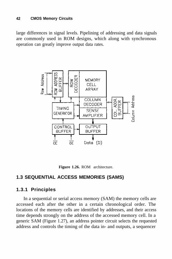
42 CMOS Memory Circuits
large differences in signal levels. Pipelining of addressing and data signalsare commonly used in ROM designs, which along with synchronousoperation can greatly improve output data rates.
Figure 1.26. ROM architecture.
1.3 SEQUENTIAL ACCESS MEMORIES (SAMS)
1.3.1 Principles
In a sequential or serial access memory (SAM) the memory cells areaccessed each after the other in a certain chronological order. Thelocations of the memory cells are identified by addresses, and their accesstime depends strongly on the address of the accessed memory cell. In ageneric SAM (Figure 1.27), an address pointer circuit selects the requestedaddress and controls the timing of the data in- and outputs, a sequencer

Introduction to CMOS Memories 43
circuit controls the order of succession of addresses in time, and a memorycell array contains the spatially dispersed data bits.
Figure 1.27. Generic SAM structure.
A SAM array is combined either of static or dynamic random accessmemory cells, or static or dynamic shift register cells. Theoretically,nonvolatile data storage cells may also be used in sequential memorydesigns. In characterization of sequential memories the input/output datarate or frequency fD and the bandwidth BW indicate the speed performancemore unambiguously than the write and read access and cycle times do.Namely, SAM access and cycle times are functions of the memory bit-capacity, the location of the addressed memory cell, the used processingtechnology and design approach. By design approach CMOS SAMs maybe categorized in three major groups: (1) RAM-based, (2) shift-register(SR) based and (3) shuffle memories.
SAM circuits based on CMOS RAM designs provide lower frequencydata rates than their SR based counterparts do, because the length of eachinput/output period is determined by the access times of the RAMs.To circumvent the access time limitations RAMs in SAMs may featurefast page, fast nibble, fast static column, extended data out or burstextended data out modes, or they are synchronous, extended, cached or

44 CMOS Memory Circuits
Rambus DRAM or SRAM designs. RAM based SAMs, by all means, havethe fundamental advantages against SR-based approaches, that RAM-cellsizes are much smaller than the corresponding SR-cell sizes, and that thepower dissipation of a RAM is a small fraction of the power consumptionof a corresponding SR memory. The small cell size and power consump-tion allow for designs of high-packing density large-bit-capacity SAMswhich can operate with rather high speed. Very high data rates,exceptionally low power dissipation and high packing density can becombined in shuffle memories.
1.3.2 RAM-Based SAMs
A RAM-based SAM consists of a complete DRAM or an SRAM(Sections 1.2.2 and 1.2.7), an address counter, an address register and anaddress comparator (Figure 1.28). The address counter generates the add-
Figure 1.28. A RAM based SAM configuration.

Introduction to CMOS Memories 45
resses from 0 to N in an N-capacity SAM, and enables write or read, whenthe content of the address register and the counter are the same.The address comparator and the clock and controller unit provide thetiming signals, and the combination of the counter, comparator andregister circuits has the role of an address pointer circuit.
1.3.3 Shift-Register Based SAMs
High-speed sequential data access can be provided by shift register(SR) based SAMs. A single SR stage, however, contains at least two datastorage elements and two data transmission devices, and needs at least twoclock phases for operation. For a write or read operation, and in dynamicSRs during storage also, the entire data content of the SAM has to bemoved simultaneously. The simultaneous transfer of all data results inlarge power dissipation. Both the rather large SR-cell size and theexcessive power consumption limit the bit-capacity of SR-based SAMs.Nevertheless, the application of SRs makes possible to eliminate thedecoders, sense amplifiers, and the bitlines from the storage array.In a CMOS SR-based array, the cells drive very little capacitive loads and,therefore, very high input/output data rates can be achieved. Furthermore,with SR-based memory designs the achievement of very high radiationhardness is also possible, because SRs do not need sense amplifiers.
A typical SR-based SAM (Figure 1.29) includes a word-or-block-widebarrel shift-register array, a clock generator, an address counter andinput/output control and buffer circuits. Input/output data may betransferred serially bit-by-bit or parallel word-by-word depending on thestate of the SPD signal. A W/R signal controls write or read operations, anM signal selects masked or unmasked write or read, and an R signalallows data recycle in the array. In an N x M bit array, with clock phase φ1
the data from the input/output register, or from the last N-th M-bit column,are transferred into a first M-bit column, and simultaneously the datacontent from every second column storing complement data aretransferred into their neighbored odd numbered column 1,3,...N-1. Duringclock phase φ2 the data content of all columns storing true data aretransferred simultaneously into their neighbored even numbered column,and so forth with consecutive φ1 and φ2 clock phases. Always two

46 CMOS Memory Circuits
neighbored columns contain a single one of each data word after the data
Figure 1.29. A typical SR-based SAM architecture.
transitions are accomplished. Thus, only N/2 number M-bit words can bestored and shifted in an N-column by M-bit SR-based SAM. The data shiftin an SR-based SAM may be made plausible in a 4 x 4 bit array, i.e., in an8 x 4 cell array (Table 1.4), in which the initial data content of the storagecells is represented by numbers, and the storage cell locations correspondto positions in the matrix. The location of a word is pointed by an addresscounter, which can be controlled for serial or parallel address reception by

Introduction to CMOS Memories 47
an SPA signal. PR signals program the speed of two clock signals CL1and CL2. CL1 and CL2 provide the two basic operation phases φ1 and φ 2 ,and serve as references to various clock signals required for the operationof the memory frequencies. The chip-enable CE signal keeps the memoryactive, clocking may be stopped and started any time by an S/G signal,or the stop and start can be determined by the content of the addresscounter in most SR-based SAM designs.
14
24
34
44
11
21
31
41
14
24
24
44
–11
–21
–31
–41
11
–21
–31
–41
14
–24
–34
–44
1 2
2 2
–3 2
–42
12
22
32
42
11
21
31
41
11
21
31
41
–12
–22
–32
–42
12
–22
–32
–42
–11
21
–31
–41
13
23
33
43
12
22
32
42
12
22
32
42
–13
23
–33
43
13
–23
–33
43
14
24
34
44
13
23
33
43
13
23
33
43
–14
–24
–34
–44
14
24
34
44
13
23
–33
–43
Phase 1
Phase 2
Table 1.4. Barrel-shifting in a 4 x 4 bit (8 x 4 memory cell) array.
The SR operation allows for gapless streams of input and output datawhich appears synchronized with the applied master clock without a

48 CMOS Memory Circuits
latency time. Between the appearance of the clock and a read signals thedelay is very small, while the write data may be required to somewhatprecede the clock at high frequency operation.
The maximum clock frequency, at which an SR-based SAM canoperate, depends on the design of the SR-cell, the SR array and the datainput/output circuits. Since each word of data is transferred between twoneighborhood columns, no small sensing signal is required, and the wholememory can be designed of digital logic gates. CMOS circuits designed ofdigital logic gates provide considerable larger noise and operation marginsthan CMOS RAMS do. Therefore CMOS SR-based SAMs can be designedfor better environmental tolerance and for higher radiation hardness thanCMOS-DRAM and SRAM-based circuits.
In comparison to RAM-based SAMs, SR-based SAMs can provide10-30 times higher data rates, but they need 2-6 times more silicon areaand operate at 10-100 times higher power dissipations than RAM-basedSAMs do, if the same technology and same bit capacity are assumed,for both RAM- and SR-based designs. The bit capacity per chip in an SR-based SAM is limited primarily by the excessive power dissipation of theSR-array, which increases in accordance with the increase in operationalspeed and in bit-capacity per chip. Approximately a ten-fold increase inradiation hardness may also be expected in SAM designs which apply SR-rather than RAM-cell arrays.
1.3.4 Shuffle Memories
Shuffle memories [18] combine the advantages of both RAM- and SR-based designs including very high operational frequency, packing densityand radiation hardness, and extremely low operating power consumption.The operation principle of shuffle memories rests on a data transferalgorithm in an array, which allows the application of RAM-cells withoutthe need for bitlines and sense amplifiers in contrast to RAM-based SAMdesigns, and without the need of moving the entire data content of thearray of write and read accesses in opposite to SR-based SAM designs.In shuffle SAMs during one clock cycle, the data content of only one

Introduction to CMOS Memories 49
column is transferred into the next column, and both the input and outputregisters step only one bit to allow the input and output of one bit datum.
A basic shuffle memory array (Figure 1.30) comprises input andoutput registers, shuffle signal generator and a memory-cell array.A memory cell consists of one storage- and one transfer element. The in-and output nodes of N transfer elements couple N storage elements in achain, and the control nodes of N transfer elements are coupled to a singlewordline. The N x N memory cell array is terminated by the registers fordata input and output. Data shuffling in the array and from and to theregisters are controlled by the shuffle signal generator.
Figure l.30. Shuffle-memory architecture.(Derived from a product of Microcirc Associates.)
The shuffle signal generator may be implemented in a shift-registerwhich circulate a single log. 1 and N-1 log.0, or in a n = log²N-bit counterand an N-output decoder, or in other digital circuits.
50 CMOS Memory Circuits
In SAM operation the shuffle signal generator circuit activates one,and only one, word of N bits. In an initial clock period, the content of afirst N-bit word or a set of external data is dumped into the output register,and the datum of from the first stage of the output register is shifted intothe input register. At this time the output register holds a copy of the datacontent of the first N-bit word, and the data in none of the N-1 other wordsare moved or copied. In a next clock period, the content of a second N-bitword is transferred into the storage cells of the first N-bit word, and thesecond bit of the first N-bit word is shifted from the output register intothe input register buffer. Now, the output register holds a copy of N-1 bitsof the first N-bit word, the input register has the first bit of the first N-word, and the storage cells of the first N-word contain a copy of the datacontent of the second N-bit word, and none of the other N-l words ismoved or copied. In similar steps, N² clock periods recycles the N² bits ofthe memory cell array. The shuffle array allows for both bit-sequential orword-parallel write or read when the addressed bit or word appears in theinput or in the output register. The internal operation of a shuffle memorymay be illustrated in a 4 x 4 matrix (Table 1.5), where the initial content ofeach storage cell is represented by numbers, and the allocation of numbersin the matrix corresponds to the locations of the storage cells in thememory cell array and in the registers.
Shuffle memories, like SR-based SAM, provide continuous strings ofdata which appear in synchrony with the master clock without latency, andmay feature dual and stop-start clocking, serial and parallel data andaddress transfer, data recycling, masked write and read as well as othermemory operations. The operational speed is as fast as the speed of SR-based SAMs due to the small capacitive loads on the memory cells.Nevertheless, the bit-capacitance per chip can be as high as that of a RAM,because the shuffle memory may use RAM cells rather than SR cells in thedesign. Much less than the power dissipation of RAMS can also beachieved in shuffle memories, since only one word is activated at a time,and the activated memory cells are not coupled to highly capacitivebitlines and sense amplifiers. Moreover, the lack of sense amplifierseliminates the most difficult obstacles for radiation hardened designs.

Introduction to CMOS Memories 51
Compared to RAM-based SAM designs, shuffle memories can provide10-30 times faster data rates, about 10-1000 times less power consumptionand approximately 10 times higher radiation hardness than RAM-basedSAMs do, and the bit-capacity per chip of shuffle memories can near thatof RAM-based SAMs.
11 11 12 13 14
21 21 22 23 24
31 31 32 33 34
41 41 42 43 44
21
31
41
12 12 13 14
22 22 23 24
32 32 33 34
42 42 43 44
11
21
31
12 12 13 14
22 22 23 24
32 32 33 34
42 42 43 44
Table 1.5. Principle of data-shuffling in a 4 x 4 bit (4 x 4 memory cell) array.
1.3.5 First-In-First-Out Memories (FIFOs)
A first-in-first-out (FIFO) memory is a sequentially accessible write-readdata storage device, in that data rate for writing can substantially differ from
Step 1
11
Step 2
11
21
Step N²-1
41

52 CMOS Memory Circuits
the data rate of reading while keeping the same sequence of data transfer inboth write and read. If the data sequence of read is the opposite of the writedata sequence, the device is called last-in-first-out (LIFO) memory. Inessence, FIFO and LIFO memories are data-rate transformer devices, butLIFOs reverse also the data sequence. Transformation in both data rate anddata sequence may beneficially be applied in designs of digital systems.Therefore, numerous FIFO designs allow for a variety of output datasequences which can be generated from one input data sequence in additionto performing data rate transformations and other features. FIFOs mayfeature data write and read on both the inputs and outputs, as well as datareset, and flow-through, and expandable word-width and memory-length.
A FIFO memory is applied most often, as an interface between twodigital devices DA and DB to temporarily store the data received from D A
until DB is ready to accept. The FIFO’s storage capacity must be largeenough to accommodate the amount of data that D A generates betweenservices, and the FIFO has to perform the write operations with the clockfrequency of D A and the read operations with the clock rate of D B .Either one, or both write and read, may operate synchronously orasynchronously.
FIFO operation can be obtained, most trivially, in shift registers,if there is no requirement for independent writing and reading. Writing isclocked by device DA , the received information is shifted until the firstdata bit or word is available at the output, and the data is shifted out withthe clock rate of device DB .
Most FIFO devices, nonetheless, are modified RAMS (Figure 1.31) inwhich the addressing is word-sequential. Rather than using addressesreceived from another circuit, a FIFO chip internally generates addresssequences in the write and read address pointer circuits. Address pointersare usually digital counters or shift registers used independently for writeand read. Thus, writing and reading can be randomly intermixed, but onlyone operation, write or read, can be performed in one clock cycle, becauseonly one address can be selected at a time. An address generated by thepointer circuit is decoded, and enables a row or word in the memory cellarray. The enabled row can receive the content of the input register, or

Introduction to CMOS Memories 53
send its stored information to the sense amplifiers and the output register.The input and output register operations are governed by the write and read
Figure 1.31. A modified RAM as FIFO memory.(Derived from a product of Quality Semiconductor Incorporated.)
control circuits, respectively. These control circuits accommodate the ex-ternal clocks, synchronous and asynchronous enable signals for each writeand read operation. Flag signals indicate how much of the RAM storagecapacity is occupied, e.g., empty, full, almost empty, almost full, etc., andthe amount of flagged storage capacity can be programmed in most FIFOs.Both the depth and width of the FIFO storage array may be extended by

54 CMOS Memory Circuits
coupling a multiplicity of FIFOs to each other through the expansionlogic. The content of an FIFO may be bypassed in designs where offsetregisters are implemented.
FIFOs implemented in two-port RAMS, rather than in traditionalRAMS, are capable to handle write and read operations simultaneously.In such a FIFO the write and the read address code has independent sets ofaddress inputs. The dual addressability requires the use of complex andlarge memory cells, which increases chip size and costs of FIFOs. A FIFOarchitecture that is based on dual-port RAMS is similar to the FIFOarchitecture using single-port RAMS, except the difference in write andread addressing.
1.4 CONTENT ADDRESSABLE MEMORIES (CAMS)
1.4.1 Basics
In associative or content addressable memories (CAMS) [19] data areidentified and accessed by the data content of a multiplicity of memorycells rather than by addresses. Associative memories address dataelements, or words, in their memory cell array by associating input datawords, or keys, with some or all the stored words (Figure 1.32). The inputword is stored in an argument register. A mask register can excludearbitrary "don't care" bits from the associative search. The result of theassociative search is a flag signal that indicates match or mismatchbetween the masked search argument and an interrogated word located inthe CAM array, and this flag signal is transferred into a response store.When more than one flag signals indicate matches, a multiple responseresolver establishes a sequence for the further processing of the matchingwords. Further processing may also require the use of both the matchedwords and the addresses of the matched words, therefore output buffer andan address encoder are also parts of an associative memory.
Associative search can determine not only an exact match, i.e., all bitsare identical in the compared words, but also the degree of similarity in apartial match. For similarity measure CMOS CAMS use mostly theHamming distance, which simply gives the number of bits the comparedwords differ from each other, but CMOS CAMS may also apply Euclidean

Introduction to CMOS Memories 55
Figure 1.32. Associative-search in a CAM.
distance, Minkowsky metric, Tanimoto-measure and various algebraic andlogical correlation measures. The measure of similarity may provide thebasis for the operation-strategy of the multiple response resolver.In practice, however, multiple responses are resolved mostly by usingspatial or timing orders rather than by similarity measures. To establishsimilarity magnitudes repeated search for the same search argument atsystematic masking is required in all CAMS.
From the wide variety of potential CAM applications data contentassociations, magnitude search, catalog memory and information retrievalare only the most apparent examples of use. CAM circuits are often usedalso in cache memory implementations. Moreover, entire computerimplementations are based on associative circuits [110]. Partly-associativecomputations are routinely applied in object and voice recognition and innumerous other military, government and forensic systems. Generally, for

56 CMOS Memory Circuits
systems which would be unacceptably slow or complex with traditionalVon Neumann type of computations, the application of CAM-basedimputing systems may be attractive design alternatives.
CAMS, most commonly, are categorized as (1) all-parallel, (2) word-serial-bit-parallel, and (3) word-parallel-bit-serial classes. The implemen-tation of all types of CAMS, except the all-parallel CAM, can be based onany type of random or sequentially accessible CMOS memory designs,including all types of RAM, shift-register and shuffle memory arrays. Thedominance of RAM technology and the excellent performance-costparameters of RAMS, nevertheless, give little chance to justify the use ofany other approach than the RAM-based design to CAM implementation.What is more, in many designs, CAM functions are provided by software,e.g., hash coding, TRIE, etc., so that traditional RAM or SAM hardwarecan be used.
1.4.2 All-Parallel CAMS
The all-parallel CAM compares the search argument with all wordsresiding in the CAM simultaneously. The simultaneous comparison ismade possible by combining a RAM cell with an exclusive-OR (EXOR)gate in a single CAM cell, and the outputs of the EXOR gates are tied toan interrogation line in each word. In practical designs, the elements of theRAM cell and the EXOR gate are blended with each other to decreasecomplexity and size of CAMs.
An all-parallel associative memory consist of a (1) content addressablememory cell array, (2) search argument register, (3) mask register,(4) response store, (5) multiple response resolver, (6) write and readcontrol, (7) address decoder, (8) address encoder, and (9) output buffer(Figure 1.33). Addressing allows to access CAM cells by word addresses,and addresses are needed to facilitate and control a variety of CAMoperations. Initially, a CAM array is addressed word-by-word, and eachdata word held in the search argument register is written into the CAM cellarray. At an associative search, the data content of the search argumentregister is compared with all or with a required fraction of the wordsstored in the CAM cell array. Where the search argument word matches

Introduction to CMOS Memories 5 7
the masked content of a word stored in the array, match signals occur.The match signals are put in the response store, prioritized by the multipleresponse resolver, and the addresses of the matching words are encodedfor further nonassociative operations.
Figure 1.33. All-parallel CAM architecture.
The all-parallel associative memory executes the data search in oneshort cycle. The length of the search cycle tS is determined by theconsecutive delays occurring in the search argument and mask registers ti,in the CAM array t , in the response store and multiple responseCAM
resolver (t ), and in the data output buffer tres o as:

58 CMOS Memory Circuits
The longest data propagation delay appears in the CAM array,in which the delay time depends mainly on the bit-capacity of the arrayand on the CAM-cell design. Since full featured CAM cells are muchmore complex and larger than RAM-cells are; for CAMs the practicallimit of bit capacity per chip is much smaller and the power dissipationsper chip is much larger than those for RAMs.
1.4.3 Word-Serial-Bit-Parallel CAMs
Any RAM array can be used to implement word-serial-bit-parallelCAMs. In such a CAM, a parallel-operating digital comparator is placedbetween the mask-register and the RAM-cell array, preferably next to thesense amplifiers, and an address counter generates a sequence of word-
Figure 1.34. A word-serial-bit-parallel CAM configuration.
Introduction to CMOS Memories 59
addresses to the RAM-cell array (Figure 1.34). One-by-one each word iscompared to the search argument and the responses are transferred in ashift register. The shift register content preserves the time sequence ofmatches, and, therefore, it may also be used as a multiple responseresolver. Since the responses appear serially, the maximum search cycletime tS to associate N-words with a search argument, comprises N timesthe wordline, bitline and sense amplifier delays in the RAM array t RAM,and N times the comparison delays tcom in addition to t i , t res and t o:
Very short search times can be combined with exceptionally smallpower dissipations and high packing densities in designs which applyshuffle memory arrays in place of the RAM-cell array. The RAM-cellarray may also be substituted by a shift-register array, but shift registerarrays are plagued with low packing density and hefty power dissipationsat high frequency operations.
1.4.4 Word-Parallel-Bit-Serial CAMs
Word-parallel-bit-serial CAMs may also be implemented by applic-ation of RAM-cell arrays similarly to the previously introduced word-serial-bit parallel CAMs. Word-parallel-bit-serial CAM designs applyeither modified RAM cells in the array or the arrays have to be subdividedinto subarrays, and each individual subarray has to include a specificdecoder circuit. The high circuit complexity, and the resulting low packingdensity and moderate performance, make RAM based world-parallel-bit-serial CAMs less attractive than other CAM implementations. Excellentspeed performance can also be obtained by application of a barrel shift-register array, but because of packing density and power considerationsshift-register arrays should be kept in small bit-capacity. Large bit-capacity can be combined with very low power consumption and veryhigh data rate by implementations in shuffle memories.
Since both shift-register and shuffle memory clock data bits in and outof the circuit one-by-one in the same order, the operations of both shift-register- and shuffle-memory-based CAMs may be illustrated in the sameblock diagram (Figure 1.35). In this word-parallel-bit-serial CAM array,

60 CMOS Memory Circuits
the word, search argument and mask data may be written either in series orin parallel mode into the registers. All registers are the same, and in all
Figure 1.35. A word-parallel-bit-serial array.
registers the data are moved and circulated by the same clocksimultaneously. In the response processor, one bit of each word iscompared simultaneously to the masked search argument, and the result isstored and evaluated as the data circulates in the registers. Except the datastorage and associative search circuits, a word-parallel-bit-serial CAM canhave the same constituents as the all-parallel and word-serial-bit-parallelCAMs do.

Introduction to CMOS Memories 61
In this word-parallel-bit-serial CAM, the maximum search cycle t S forN words of M bits, includes M-times the data advance time for one bit tD
and the signal delay in the response processor t in addition to the input,RP
output and resolver time ti, to and t :res
The magnitude of tS greatly depends on the speed of the responseprocessor and the shift-register or of the shuffle memory.
1.5 SPECIAL MEMORIES AND COMBINATIONS
1.5.1 Cache-Memory Fundamentals
A cache-memory, or cache, is a short-access-time small-bit-capacitymemory that temporarily stores a fraction of the data and instructioncontent from the overall memory content of a computing system.Cache memories are applied in traditional Von Neumann type ofcomputers to improve their performance, i.e., to narrow the gap betweenthe high operational speed of the computing unit and the low input/outputdata rates of the main memory (Section 1.1). Generally, the greater thestorage capacity of a memory is, the longer are the access, cycle and datatransfer times and the slower are the memory input/output data rates.Slower memory operations cause more idle runs in the central computingunit (CPU). Placed between the CPU register and the main memory, acache or a complex of cache memories (Figure 1.36) can decrease the timethe CPU receives instruction and data and, thereby, it can improve thespeed and efficiency of computing systems. System performanceimprovement by cache applications, nevertheless, requires increase insystem complexity, i.e., the addition of cache memory and controller.
One level of cache may not be sufficient to provide a required systemperformance. In systems using multi-level cache hierarchy the cacheclosest to the CPU is denoted as primary or level-one (L1) cache, while thecache coupled to L1 is the secondary or level-two (L2) cache and so forth.Caches on an arbitrary i level (Li) can contain either the instructions (LiI),or the data (LiD) or both (LiID).

62 CMOS Memory Circuits
Figure 1.36. Cache memory application in computing systems.
The applicability of any cache LiI, LiD and LiID are based on the(1) temporal, and (2) spatial locality of the instruction and data items.Temporal locality means that items used in the recent past are likely to beused in the near future, while spatial locality implies that items placedphysically near to each other are likely to be used in consecutiveoperations. The efficiency of cache operations depends on the probabilitythat the item when requested by the CPU is in the cache or not, and the

Introduction to CMOS Memories 63
cache performance is characterized by the hit rate and miss rate and by thememory cycle times. A hit occurs when the item is found in the cachewhen the CPU requests it, and miss appears when the cache does notcontain the referenced items during the time of their request. The numberof CPU references which result hits divided by the total number of CPUreferences gives the hit rate HR , and the miss rate MR may be expressed asM . An increasing hit rate decreases the total number of CPU cyclesR=1-HR
needed to execute an instruction, and improves system performance.Nevertheless, the performance of a system, that includes cache, dependsalso on the number of CPU cycles required to fetch an item from the cacheat a hit and from the main memory in case of a miss. Therefore, both thecache and main memories should be designed so that they operate with theshortest possible memory cycle times. What is more, the signalpropagation times between the main and cache memories, between theCPU register and the cache and also between the CPU and the mainmemory, should also be short.
A memory address code contains bits to determine the location ofwords within blocks, blocks within sections, and sections within the cachememory. A block or a line includes a certain number of words, as well as anumber of tag bits which uniquely determine the location of the block inthe main memory. An address tag is applied to indicate which portion ofthe main-memory content is present in the cache, and it may contain eithera part of the address bits, usually the most significant address bits, or all ofthe address bits. The number of tag bits depend on the size of the blocksand the bit capacity of the main memory. To reduce the number of tag bitsthe block sizes may be increased, or the blocks may be grouped in sectionsand only the sections are tagged. A collection of blocks or sections,for which the tags are checked simultaneously or parallel in a cachememory, is a set. The number of blocks in a set is the degree ofassociativity or the set size of the cache.
Performance improvements by cache memory applications havebecome an important part of the system design and are discussed inpublications extensively, e.g., [111]. The following discussion focuses onthe architectures of CMOS cache memories.

64 CMOS Memory Circuits
Cache hit rates can be improved by optimizing both organizational andstrategical variables. Organizational variables include the data storagecapacity C, number of blocks in a set or degree of associativity A,number of sets S, and block size in bytes or bits B of the cache. Increasingcache capacity C = A x S x B, increases the probability of hits. A simpleincrease in cache size C would result in longer cache operation times. In alarge cache, yet, the cycle time can be kept short by increasing the numberof blocks per set A and by decreasing the amount of data stored per tag B.Clearly, variables C, A, S, and B can be optimized in a system.The performance of the system may also be ameliorated by careful choiceof strategies in replacement of blocks in the cache (last recently used LRU,first-in-first-out FIFO, random, etc.), in data writing (copy back to main-memory, write through cache to main memory, buffer several writes, etc.),in data fetching (number of blocks, speculative prefetching, order of datareturn, etc.), and in workload management (adjusting block sizes,request buffering, system timing, etc.). System strategies for optimumperformance may substantially vary system to system, and the chosenstrategies determine a great part of the overhead circuit design in the cachememory. Since the optimum cache memory size, associativity, block-size,set-size as well as strategies of replacement, writing, fetching andworkload management are actually system dependent, the optimization ofthese parameters are not discussed here, but they are available in theliterature of computing systems, e.g., [112].
CMOS caches are not only fast-operating small-size memories withthe ability to determine quickly whether the requested instruction or dataare stored in the cache (hit or miss), but they are also capable to replacethe stored items by items fetched from a main memory if the requesteditem is not found in the cache memory. Since the cache is a temporarybuffer for a portion of the main-memory content, the data in the cachehave to be coherent with the data in the main-memory. Common coher-ency strategies are the copy-back and write-through policies.
Under the copy-back policy, the cache records writes and reads, andthe cache can operate without using the circuits of the main-memory.An update of the main-memory occurs when the data block that containsthe write address in the cache is replaced. No replacement can be

Introduction to CMOS Memories 65
performed in cache locations which are occupied and flagged by a "dirty"signal indicating that the information must be written into the main-memory, otherwise they would get lost. With the copy-back strategy, themain-memory is updated far less frequently than with other coherencystrategies, but the replacement of information in the cache requires thetransfer of large amount of data and, thereby, rather long time for eachtransfer event.
In the write-through policy the reads are cached, but the writes arestored in the main-memory, and in write cycle the main-memory isaccessed. This ensures coherency between the cache and the main-memoryoperations, but the large number of slow accesses to the main-memorydecreases the system performance. In the majority of computing systemsthe use of the write-through policy is less efficient than the application ofthe copy-back strategy.
1.5.2 Basic Cache Organizations
CMOS cache memory designs, like other cache memory implementations,may be fully-associative, direct-mapped and set-associative.
In a fully-associative cached computing system, the main memory andthe cache are divided into storage blocks, and the cache stores one set ofblocks. Any block in the main memory can be mapped into any block in afully-associative cache memory (Figure 1.37). The fully-associative cachecompares simultaneously each bit in every tag stored in the cache to eachbit of the effective or physical address generated by the computing unit,to determine a cache hit or miss. The cache performs a fully associativetag comparison, and the tag memory is designed as an all-parallel contentaddressable memory. Fully-associative cache memories are capable tokeep the most frequently accessed data and instructions, no matter in whatlocation of the main memory these data and instructions are stored.However, to find the desired data and instructions the entire cache must besearched, and this search-time compromises the performance of thefully-associative cache.

66 CMOS Memory Circuits
Figure 1.37. A fully associative cache organization.(Derived from a product of Microcirc Associates.)
In a direct-mapped cached system each storage block of the cache islinked to several predetermined blocks of the main memory. The direct-mapped cache memory has a tag and information store, and a comparatorfor matching the tag bits of the addresses (Figure 1.38). The block addressis broken into tag and index bits. The index bits are the addresses in the

Introduction to CMOS Memories 67
cache memory and determine the depth of the cache. Cache locationscorrespond to predetermined main-memory locations which are identified
Figure 1.38. A direct mapped cache configuration.
by the same index bits. Because the use of index bit reduces the number ofbits to be compared, the detection of a cache hit or miss is fast. A direct-mapped cache, however, can not maintain a nearly optimal collection ofblocks, because the new block, that replaces an old one, determines whichone of the old blocks has to depart. Furthermore, if the block required tobe in the cache is the same as the one used in the preceding program stepexcept this block is requested from a different set, the block has to befetched from the main-memory and written into the cache. In such cases,the direct-mapped cache has frequent misses and operates inefficiently.

68 CMOS Memory Circuits
A set-associative cache operation alleviates the contentions of thefully-associative and the direct mapped systems, keeps the tag-memorysmall and the tag comparison simple and speedy, by dividing the cache'smemory capacity into N direct-mapped sets, and by using N number ofsimultaneously operating comparators. In a two-way (N=2) set-associativecache (Figure 1.39) both of the RAM arrays, decoders, comparators andinput/output registers are identical. Furthermore, identical are thepredetermined locations in both RAM arrays in which the main-memoryblocks can directly be mapped, and blocks from a certain main memorylocation can be copied into two cache locations. If the tag-bits of theaddress match either one or both of the tags residing in the cache, then ahit occurs. At a miss, the set-associative cache can maintain a favorable setof blocks, because the cache user is free to decide which one of the blockswithin a set should be replaced. The application of four-way (N=4) set-associative caches represents a good balance between performance andcost in memory systems.
Whether a set-associative, or a direct-mapped or a fully-associativecache memory provides a required hit rate and the most economicalsolution, it depends on specific system parameters. Therefore, manyapplication-specific cache designs are available, and many designs allowto change between set associative and direct mapped organizations, or touse fully-associative caches also in direct-mapped in set-associativeoperation modes by one or two external control signals.
Cache operation may also include error detection and correction by theapplication of simple error correcting codes and a few redundant bits foreach block. Additional status bits may also be required to record the time-order of the tag-usage, or to store other information which assist thereplacement of the cache's information content. Cache designs oftencomprise multiplexers to avoid repetitions of significant circuit parts in thelayout and, thereby, to keep the chip-size of the cache small. Many cachesuse multiplexing also for accommodating certain input and output dataformats. Data formats, block- and tag-sizes may be programmable to allowfor adjustments in system optimizations.
Requirements for fast system operation and ease in applications pointto the use of SRAMs in cache designs. Nevertheless, cache designs can

Introduction to CMOS Memories 69
apply any type of fast operating memory circuits, e.g., small-size DRAMswhich have the potential to approach the access times of SRAMs.
Figure 1.39. A two-way set associative cache architecture.(Derived from a product of Micron Incorporated.)

70 CMOS Memory Circuits
1.5.3 DRAM-Cache Combinations
The integration of a DRAM with a cache memory in a single CMOSchip is aimed to combine the low cost per bit of DRAMS with the highbandwidth of cache memories. A DRAM-cache combination improves theoperational speed of computing systems by both means: (1) by the widebandwidth of the integrated cache and (2) by the greatly reduced datatransfer time between the DRAM and cache memory. Small SRAM cacheshave wide band widths due to their inherently high speed write and readoperations, and due to their large word size designs. Furthermore, thecontinuity of the write and read operations are infrequently halted, as aresult of the high probability that the requested information is stored in thecache at the time of the request. If the requested information is not storedin the cache, a rapid instruction and data transfer is required to update thecache. In DRAM-cache combinations, this transfer of instructions and datacan be very fast due to the lack of chip-to-chip interfaces, and due to thevery short chip-internal wire-lengths between the DRAM and the cache.
The most publicized DRAM-cache combinations are the (1) enhancedDRAM (EDRAM), (2) cached DRAM (CDRAM) and (3) Rambus DRAM(RDRAM) and (4) virtual channel memory (VCM).
1.5.4 Enhanced DRAM (EDRAM)
The EDRAM (Figure 1.40) blends a primitive one-row (X bit) widecache directly into the column decoder of the DRAM. It caches one row ata time, but in a three dimensional X x Y x Z memory array organization itmay cache X x Z bits. On every cache miss, the EDRAM loads a new rowinto the cache, most frequently, on a last row read (LRR) basis. Thus, anLRR register and a comparator are also added to the genericDRAM design.
An EDRAM writes directly to the DRAM, but reads from the cachememory. During a burst read the EDRAM provides data burst B<<X, andhides the precharge cycle of the DRAM. The precharge is completedbefore a consecutive burst-read can start. To read the cache no row enablesignal is needed, when the cache has hits. At cache misses the EDRAM

Introduction to CMOS Memories 71
accesses the DRAM. The DRAM cell can be refreshed without anywaiting time during write, read and burst-read operations.
Figure 1.40. EDRAM organization.(Derived from a product of Ramtron Incorporated.)
The differences between DRAM and EDRAM operations aremanifested in differing operation controls. An EDRAM may include chipselect S, row enable RE, column address latch CAL, refresh F and separateoutput enable G control terminals which enhance the application flexibilityof the built-in cache. Since the cache is a part of a DRAM architecture,

72 CMOS Memory Circuits
most EDRAMs operate asynchronously, although synchronous EDRAMmay also be designed with little added effort.
1.5.5 Cached DRAM (CDRAM)
A CDRAM integrates a complete cache memory and a generic DRAM,so that the cache and DRAM can operate independently. In a typical design(Figure 1.41), between a (2m x D)-bit DRAM and a (2n x D)-bit cache arow-wide buffer of D² bit capacity is applied, and each of the DRAM andthe cache has a separate control circuit. The cache is directly addressed by naddressing bits, while the DRAM addressing is multiplexed in a ratio ofm/n. Between the DRAM and the cache a buffer facilitates communication.
Figure 1.41. A CDRAM architecture.(Derived from a product of Mitsubishi Electronics America Incorporated.)

Introduction to CMOS Memories 73
A half of the buffer-bits serves read-data transfers, and the other half of thebits serves write-data operation transfers from and to the DRAM. All bufferbits are used for data transfers between the buffer and the cache memory.
The cache is segmented into D²/2 cache lines with D words per line,and can be either direct-mapped or set-associative depending on theimplementation of the external cache controller. At a cache hit, D bit ofdata is transferred through the buffer to the output. At a cache miss thebuffer receives D²/2 bits simultaneously from the DRAM either in write-through or write-back replacement mode. The write-back cycle may behidden by buffering. At a write miss, the buffer data can be posted duringa complete DRAM write cycle.
A CDRAM may use a synchronous clock to control all operations. Allcontrol and address signals should be set up before the appearance of theclock signal, and access and cycle times are from and to the appropriateedges of the synchronizing clock signals. The synchronous output registermay operate in transparent, cached, registered and masked modes.
1.5.6 Rambus DRAM (RDRAM)
The RDRAM unifies a synchronous DRAM, a row-cache and a com-plete data-bus interface circuit (Figure 1.42) [113]. The on-chip interfacecircuits greatly reduces the communication time between the DRAM andthe other parts of the computing system, in addition to the performancebenefits of integrating the cache and the DRAM in a single chip. RDRAMapplication and operation in systems are determined by specific protocols,which allow to combine the addressing, data commun-ication and controlsignals through a single bus complex.
In RDRAMs write and read operations include bus request, data andacknowledgement of data arrival. At read, positive acknowledgementmeans that the requested data are in the cache, negative acknowledgementappears if the data are not in the cache or a refresh cycle is in progress.At a second cache miss, upon a consecutive read-request, the RDRAMissues a write request to the cache from the DRAM. A write into theRDRAM commences also with a request for data package. When the write

74 CMOS Memory Circuits
data can be accepted by the RDRAM, positive acknowledgement occurs.Negative acknowledgement may appear when the write address is notfound in the cached page, or when a refresh cycle is in progress during thewrite request. After the first write request the controller waits a DRAMcycle and repeats the write request for the same data and address.
Figure 1.42. RDRAM scheme. (Inferred from [113].)
In the proprietary Rambus systems (Figure 1.43), the data, address,control and clock signals can be transferred at very high frequencies,e.g., at 800 MHz. At high frequencies the bus, clock and otherinterconnect lines behave as transmission lines (Sections 4.1.3 and 4.1.4),in which the propagating signals have significant delays or flight times,and can greatly be distorted by reflections on the interfaces and, in smalldegrees, by attenuations within the lines. Different flight times for thedata, address, control and clock signals, and distorted signal forms,would make a system inoperable and, in unfavorable combinations,even damaged. Rambus systems counteract the effects of transmissionlines by the use of a folded clock signal path and of resistive line

Introduction to CMOS Memories 75
terminals. For flight time compensation the folded clock signal pathprovides forwards and backwards signals along the bus lines.Forward clock signals are applied in read operations, because the read datapropagates from the RDRAMs to the control unit. In write operationbackward clock signals are applied, because the write data runs toward theRDRAMs. For minimizing the effects of signal reflections all signal andclock bus lines are terminated by resistors RT -s which are connected to aterminal voltage. The termination resistors keep reflections under controland determine the signal amplitudes on the bus and clock lines. All busand clock lines are expandable up to a functional limit, e.g., 10 cm,
Figure 1.43. RDRAM system with Rambus protocol [114].(Derived from a design of Rambus Incorporated.)
to accommodate various numbers of RDRAMs. The operation of theRDRAMs are controlled by different protocols in the base, concurrent anddirect Rambus systems. Since the Rambus systems use pocket codes, theyare referenced as pocket protocol systems.
Other protocol based memory and system architectures, e.g., SynclinkDRAM, an implementation of the Ramlink protocol [114], differ littlefrom the RDRAM and the Rambus protocol in concepts. While theRambus concept applies single ended terminals and linear extension of thebus wires and the number of RDRAMs, the Ramlink concept applies aclosed ring bus structure in which the extension of the bus and the number

76 CMOS Memory Circuits
of Synclink DRAMs, or SLDRAMs, are confined in the ring. Synclink, asRambus, is also a pocket protocol system. Extended performance can beobtained by protocol implementations which use small-signals anddifferential signal-pairs in data transfers.
1.5.7 Virtual Channel Memory (VCM).
A VCM combines a DRAM, preferably a dual- or a multibanksynchronous DRAM, with a multiplicity of cache SRAMs (Figure 1.44) in asingle memory chip. The K number of cache SRAMs create K number ofvirtual channels, and to each channel the computing system assigns adistinguished task. e.g., in a graphics system one channel is for reading displaylist, another one is for loading texture maps and a third channel is for loadingvertice data. Data transfers between the SRAMs and the DRAM have toexplicitly be ordered by a VCM-external memory controller in contrast toEDRAMs, SDRAMs and RDRAMs, which manage SRAM-DRAM datatransfers chip-internally. The cache SRAMs are placed next the DRAM so thatthe X number of SRAM columns joins through minimum wire-lengths to theX number of the DRAM's sense amplifiers. In this SRAM-DRAMcombination, only the cache SRAMs need an X-output column decoder foraccess, while a single row- and a segment-decoder support the wordlineselection in the DRAM. For the selection of an SRAM a channel selectorcircuit is used. Each virtual channel has its own interface circuits anddedicated resources to accommodate the operation modes. The operationcontrol of the VCM requires a control logic circuit which is more complexthan that of other DRAM RAM designs.
In a VCM design, the circuits which surround the DRAM array areorganized to hide the precharge time, or precharge latency, by pipeliningthe operations of the individual cache SRAMs. The precharge time in aDRAM array is several times longer than the access time for the bits in acertain selected row or in a page (Section 1.2.2). Upon a change in pageaddress, the first write or read of a memory cell can be performed onlyafter the precharge is completed, because all the three write, read andprecharge operations use the same bitlines and sense amplifiers. Bits in apage can be addressed with high frequency, e.g., one or two bits with

Introduction to CMOS Memories 77
Figure 1.44. A VCM organization.(Derived from a product of NEC Electronics Incorporated.)

78 CMOS Memory Circuits
every system clock, without precharge latencies (Section 1.2.4). Althoughthe DRAM precharge times are unchanged by the VCM organization,during the precharge the virtual channels perform operations which do notinterfere with the precharge and can be controlled so that their operationtimes conceal the precharge latency. An intelligent memory controller canassign a well-localized code thread to each of the cache SRAMs andprotect them from page-address misses triggered by other memoryaccesses. Page-address misses may often occur when multitask operationsforce the memory to write and read information into and from randomlyaddressed memory locations which are far from each other in the memoryspace and in time of use. Spatial and temporal coherency are improved,here, by storing the components of a specific task in the same cacheSRAM and processing the data of this specific task through the samevirtual channel.
Apart from SRAMs the virtual channels may also be implemented insmall DRAMs or in parallel-serial registers, and a VCM may be designedfor synchronous or asynchronous operations. The precharge operationsmay also be pipelined for the segments of the DRAM, which may reducethe bit-capacity requirements in the channels of the VCM.
VCM designs may adopt a variety of input and output interfaceschemes including the traditional unterminated CMOS or the terminatedRambus, Synclink and other interfaces. As an alternative to Rambus,VCMs and numerous other high-speed memory designs may support thebidirectional stub series terminated logic SSTL interface complex [115](Figure 1.45). The bidirectional SSTL interface applies series resistorsRS -s and two termination resistors RT -s to approximate a match with thecharacteristic impedance Zo of the transmission line. Signal lines areterminated to the terminal voltage VTT, and reference voltage Vref is used todistinguish logic levels. Usually, VTT = Vref =V DD /2, where VDD is the supplyvoltage to the system. In this system, logic levels fluctuate with thevariations of VT and each memory device is activated in accordance withthe flight time of the clock impulse from or to the driver/receiver. At write,the driver provides a data-strobe signal toward the memories while at read,the data-strobe signal is driven by the memories toward the driver/receiverto compensate the flight times. This type of data-strobe technique allows

Introduction to CMOS Memories 79
to use both the rising and falling edges of the clock signals as references tostart write or read operations. Since traditional systems timed only by theleading edge of the clock signal, the use of both clock-impulse edges candouble the data rates in compatible memories. Memories which canoperate with such double data rates are called double data rate DDRdevices. In practice, DDR techniques do not double the achievable datarate in DRAM operations, because each write and read access is precededby a latency time. Critical is the row latency, that is influenced by thesignal delays in the input buffer, decoders, word and bitlines, and senseamplifiers, and the latency time can greatly be reduced by highlysegmented and by hierarchical organization of the memory cell arrays.
Figure 1.45. Bidirectional stub series terminated logic interface .

80 CMOS Memory Circuits
1.6 NONRANKED AND HIERARCHICAL MEMORYORGANIZATIONS
All of the CMOS memory types can be organized in nonranked andhierarchical memory architectures. In nonranked or nonhierarchical archi-tectures each subarray has equal organization ranks, and a one-level de-coding for each row and column selection is sufficient to access any of thewords and any of the bits in the array. A nonrankd array may be simple(Figure 1.46a). or segmented (Figure 1.46b), but in both nonranked array
Figure 1.46. Simple (a) and segmented (b) nonranked arrays .
types each word and each bit of a word are directly accessible through theuse of a single-level array decoder. The hierarchical organization, in a

Introduction to CMOS Memories 81
memory chip, partitions the memory cell array into subarrays (Figure 1.47),the subarrays into sub-subarrays, etc., and divides the decoding into a certainnumber of levels [116]. The division ratio, i.e., the number of subordinate
Figure 1.47. A hierarchical memory organization with shared decoders.

82 CMOS Memory Circuits
arrays contained by one module of the one-level-higher ranked array, maybe the same or different for the various organizational levels. In designsthe most apparent rationale for using hierarchical organization is to reduceaccess times by architectural means. A worst case access time appears in asingle-array organized memory where the array delay Ta includes both theentire wordline delay tW and entire bitline delay tB (Figure 1.48a)
Both word- and bitline delays can be reduced to approximately tW/m andt /m by organizing the array of memory cells into m x m modules.B
Although the modularity increases the word decoding time tX by ∆ tX andthe bit decoding time tY by ∆ tY, nonetheless, the delay in the arrayorganized in m x m modules Ta¹(Figure 1.48b)
is smaller than Ta , because tX<<tW and tY<<t B . Namely, tX and tY occursin low-capacitance interconnect lines which run over field-oxide, while tW
Figure 1.48. Approximate access delay lengths in a nonranked(a) and in a two-level (b) hierarchical architecture.

Introduction to CMOS Memories 83
and tB are caused mainly by the capacitance of the high number of memorycells coupled to the word- and bitlines.
As a tradeoff for the shorter memory access time, increased layout areais required to accommodate the hierarchical decoding. In most of thedesigns, each of the row and column decoders is placed between twosymmetrical parts of the memory-cell array, because a single decoder candrive n number of memory cells by two buffers much faster than the samedecoder could drive 2n memory cells by a single buffer. Thus, a decreasein memory access time virtually without an increase in layout area may beobtained. If every quadrant of this generic bisymmetrical layout includes nx n memory cells, and each memory cell has Xo length and Yo width, thenthis module's total width X and length Y may be approached as
and
Mirroring this bisymmetrical module in both direction N times andadding decoder rows and columns for the selection of the increasednumber of segments, in an N level of hierarchical memory the totalenlarged length X¹ and width Y¹ of the enlarged memory may be approx-imated as
and
where N=2 for two levels and N=4 for three levels of hierarchy. More thanthree levels are unlikely to be used in a memory chip.
At the implementation of any level of hierarchy NXY < X¹Y¹ applies,but the area difference ∆A¹XY= X¹Y¹ - NXY is very small at high numberof memory cells per segment n² and at small number of bisymmetricallevels N. Because the number of memory cells per bitline is limited byrequired extents of operation and noise margins and by speed require-ments, many of the large memory designs apply hierarchical architectures.Generally, hierarchical organizations allow for improvements in bothoperational speed and power consumption at little trade-off in chip-size.

This page intentionally left blank.

2Memory Cells
Memory cells are the fundamental components to all semicon-ductor memories, and their features predominantly effect the chip-size, operational speed and power dissipation of memory devices. Thischapter examines the CMOS-compatible memory cells which are ext-ensively applied or have good potentials to be used in CMOS mem-ories. The examination of the memory cells comprises structural,storage-mechanism, write, read, design and improvement issues. Thestructural and operational characteristics of a memory cell set theprimary parameters for the design of sense amplifier, memory-cell,array, reference and decoder circuits.
2.1
2.2
2.3
2.4
2.5
2.6
2.7
2.8
2.9
Basics, Classifications and Objectives
Dynamic One-Transistor-One-Capacitor Random AccessMemory Cell
Dynamic Three-Transistor Random Access Memory Cell
Static Six-Transistor Random Access Memory Cell
Static Four-Transistor-Two-Resistor Random AccessMemory Cell
Read-Only Memory Cells
Shift-Register Cells
Content Addressable Memory Cells
Other Memory Cells
86 CMOS Memory Circuits
2.1 BASICS, CLASSIFICATIONS AND OBJECTIVES
of the memory.
Memory cells are the irreducible elementary circuits which are able tostore data and allow for addressable data access in a memory, and they arethe key elements in determining the characteristics of a memory device.Memory cells are applied in arrays (matrices, cores), and the functions ofmemory-cell arrays are served by all other (peripheral, overhead) circuits
Generally, a memory cell that is applicable to CMOS memory designs,comprises (1) a data storage circuit or circuit element, (2) one or more dataaccess devices and, in some designs, (3) additional circuit elements(Figure 2.1). Nearly in all CMOS memories, one storage circuit or elementis capable to hold one bit of binary information, but some storage elementsare able to store a multiplicity of binary or nonbinary data. A data accessdevice allows or disallows data read or write from and to the storagecircuit-part depending on the state of a control signal on the control nodeof the access device. Additional circuit elements may be used to improveenvironmental tolerance and to accommodate a variety of functions in asingle memory cell.
To CMOS memory applications, memory cells are classified mostly by(1) featured operation modes, (2) data form, (3) logic system, (4) storagemode, (5) storage operation, (6) number of constituent elementary devices,(7) access mode, (8) storage media, (9) radiation hardness and others(Table 2.1). From the immense variety of memory-cell types most of theCMOS write-read memories use dynamic one-transistor-one-capacitor(1T1C), static 6-transistor (6T), and static four-transistor-two-resistor(4T2R) memory cells. These three types of memory cells are appliedprimarily to implement write-read random access memories, but also tonumerous serial and special access memory designs. Small capacityserially-accessible CMOS memories employ also dynamic 6- and8-transistor shift-register (6T SR and 8T SR) cells as well as static7-transistor shift register (7T SR) and other serially accessible cells.Static 6T and dynamic 1T1C memory cells combined with a one-bitdigital comparator are the favored approaches to construct 10- and 4-transistor content addressable memory cells (10T CAM and 4T CAM).

Memory Cells 87
Read-only memory designs are based on the mask-programmable one-transistor (1T ROM) cells.
Figure 2.1. General memory cell structure applicable to CMOS designs.
In CMOS memories, the mostly used dynamic 1T1C and static 4T2Rcells are generally not full CMOS circuits, but n-channel-only memorycells which operate with the support of CMOS peripheral circuits.Memory cells formed exclusively of n-channel or exclusively of p-channeldevices, can be designed in much smaller area, and can be fabricated withless complex processes, than their complementary counterparts do. Indesigns with single-channel-type of memory cells, no added area is

88 CMOS Memory Circuits
required for isolating the n-wells from the p-wells, and capacitor orresistor devices can readily be placed above and under the transistors andinterconnects.
1. Operation Modes: Write-Read, Read-Only, User-Programmable
2. Data Form: Digital, Analog
3. Logic Systems: Binary, Nonbinary
4. Storage Mode: Volatile, Nonvolatile
5. Storage Operation: Dynamic, Static, Fixed, Programmable
6. Device Number: 1T1C, 4T2R, 6T, 10T, Others
7. Access Mode: Random, Serial, Content-Addressable, Multiple, Mixed
8. Storage Media: Dielectric, Semiconductor, Ferroelectric, Magnetic
9. Radiation Hardness: Nonhardened, Tolerant, Hardened
Table 2.1. Mostly used classifications of CMOS-compatible memory cells.
Memories, which apply both n- and p-channel devices in full-complementary circuit configurations, are designed to satisfy stringentrequirements for high operational speed, low power consumption, andradiation hardness, or to combine extra operational features with the basicwrite, store and read functions in a single memory cell. Implementationsof full-complementary memory cells in traditional CMOS processingtechnologies take rather large silicon areas. Nevertheless, the emergence ofthin-film transistor technologies allow for vertical stacking of n- andp-channel transistors and, thereby, for designs of full-complementarymemory cells in very small sizes.
In memory cell designs, the most important objective is to minimizethe size, i.e., the semiconductor silicon surface area of the memory cell.Smaller cell area decreases (1) costs per bit, (2) access and cycle times and(3) power dissipation in CMOS and other semiconductor memories.

Memory Cells 89
Cost-per-bit benefits are results of the increased number of bits which canbe stored in a memory chip of given size. Improvements in memoryoperational speed and power are consequences, chiefly, of the reducedcapacitances which result from the use of smaller size memory cells. Acell-area enlargement in the design of memory cells may be justified byrequirements for such (1) high performance, (2) operation in severe envir-onments, or (3) functional complexity which can not be provided by theuse of smaller size memory cells.
This chapter focuses on those write-read and read-only digital binarymemory cells which are manufactured with CMOS processingtechnologies in high volumes, have established a significant applicationarea in CMOS memory technology, and have, most likely, potential to beused in future CMOS memories. Of course, memory cell types other thanthe ones discussed here, have been and are being developed and applied toCMOS memory designs. Memory-cell research has become a world-wideeffort to satisfy the increasing demand for low-cost, small-size, high-performance and low-power CMOS memories for applications in standard,military, space and in other environments. Memory cells applicable to thedesigns of user-programmable nonvolatile memories are not subjects ofthis book, because the technology of user-programmable nonvolatilememories has grown to be an independent technology for itself.
2.2 DYNAMIC ONE-TRANSISTOR-ONE-CAPACITOR RANDOMACCESS MEMORY CELL
2.2.1 Dynamic Storage and Refresh
Most of the CMOS memories apply the dynamic one-transistor-one-capacitor (1T1C) memory cell in their design, because it can beimplemented in smaller silicon surface area than other memory-cell typesdo, its implementation is compatible with CMOS processing technologies,and it is able to provide good performance in memory-cell arrays.Furthermore, the 1T1C memory cell is inherently amenable for coherentdown-scaling along with the evolution of the CMOS technology, and foraccommodating data not only in binary but also in future nonbinary, multi-level, and analog memories. Principally, CMOS compatible 1T1C

90 CMOS Memory Circuits
memory cells are developed for the designs of cost-effective, high-pack-ing-density, write-read dynamic random access memories (DRAMs). Sincethe CMOS DRAM technology dominates the semiconductor industry,designs of pseudo-static random-access, sequential-access and specialtymemories use also dynamic 1T1C memory cells.
The dynamic 1T1C memory cell (Figure 2.2) employs a single capaci-tor C S to store a certain amount of electric charge that represents a datum,uses a single MOS access transistor MA1 to couple and decouple thestorage capacitor to and from other circuits, and requires a periodicalrefresh of the stored datum and a rewrite of the read datum. The chargepocket that represents a datum corresponds to a voltage difference betweenthe storage node voltage VS and the cell-plate voltage VCP, and VCP=VSS orV CP = (V DD-V SS)/2 in most of the designs. Here, VDD and V SS are thepositive and negative supply voltages and, for convenience, VCP =V SS isassumed in the following discussion of 1T1C DRAM cells.
Figure 2.2. Dynamic one-transistor-one-capacitor memory cell circuitwith the main leakage-current paths.

Memory Cells 9 1
In a DRAM cell array, leakage currents through the access device IDL,between the storage node S and the ground IGL, between node S andpower-supply pole I and between memory cells IPL CC, alter the charge andthe voltage vS(t) across CS (Figure 2.3). To avoid great changes in v (t)S
which could destroy the stored data, the capacitor C must be rewritten orS
refreshed to V in a certain time period, in the so-called refresh time tS .ref
Figure 2.3. Leakage current effects on stored voltage levels.
The maximum allowable may be calculated from the time functions ofthe storage node voltage vs(t):

92 CMOS Memory Circuits
where VS is the initial write voltage in worst case, s is the minimumstorage capacitance, ΣÎ = I is the maximum total leakageDL + IGL – IPL + ICC
current to alter VS, and ∆V is the voltage change allowed by the operatingand noise margins of the sense circuit. From the equations of vs(t) with apredetermined ∆V, the refresh time may roughly be approximated as
t ref ≈ 0.07Cs∆V/ΣÎ
in most of the sense circuit designs.
2.2.2 Write and Read Signals
Waveforms in the accessed cell and on the bitline may beapproximated by the analysis of a simple model circuit (Figure 2.4) thatconsist of a generator vg(t), resistor r(t) and capacitor c(t) in the investi-gations of both write and read operations.
Figure 2.4. Simple model to approximate write and read signal forms.

Memory Cells 93
In write operation mode a write or a sense-write amplifier switches thebitline voltage to a memory-interim standard log.0 or log.1 level.The same voltage level appears on the storage node after a transienttime; because the gate voltage signal, that turns on the n-channel accessdevice MA1, is boosted to VG ≥ VDD + VT(VBG ). High VS ≈ V DD is needed tomaximize the amount of charge stored on capacitor CS. A higher amountof stored charge can generate larger and faster signals on the bitline duringread operation, and increases the immunity of data-storage against theeffects of incident atomic particles. The assumption that a data signal hasalready reached VDD on the bitline and that VS = 0V before device MA1 isturned on, permits an approximation of the waveform of the write-datav SW(t) on node S by applying a step-function as generator signal v (t) andg
time-invariant parameters r in the simple write-read model circuitdt and CS
With these parameters the analysis of the circuit gives
Here, rdt is the drain-source resistance of the access device in the triode
region, and τ c is the time constant of the cell. From vSW (t) the rise time tr
can be approximated by the well known tr = 2.2 τc formula. For the falltime tf = tr and for the propagation delay tp = 0.5tr may be used, becauseduring writes device MA1 operates mainly in the triode region.
In read operation mode the memory cell generates the signal vg(t) onthe bitline capacitance CB. Before activating device MA1, bitlinecapacitance CB is brought to a precharge voltage VR, and the bitline isdisconnected from all the other circuits. When CS is coupled to the bitlineresistance RB and capacitance CB through a turned-on MA1, then both thestored voltage VS = VDD - ∆V and the bitline voltage VB = VPR change. For

94 CMOS Memory Circuits
calculation of the voltage-level change on the bitline as a function of timev rB(t) the rudimentary model may also be applied at read with the assump-tions
where τ B is the time constant of the bitline. The Laplace-transformed ofvg(t) and the bitline voltage vrB(t), Vg(p) and VrB(p) respectively, may beexpressed as
and
while the reverse transformation of V (p) resultsrB
Clearly, both the amplitude and the time-behavior of vrB(t) are functions of
the time constants τ C and τ B. Depending on the ratio τ B/τ C the normalized
v rB(t) curves have different voltage-maxima appearing at different timepoints, and have different switching times for each signal-swing (Figure2.5). In designs, the read-signal amplitude can most effectively beinfluenced by adjusting the storage capacitance CS and bitline capacitance

Memory Cells 95
Figure 2.5. Read-signals as functions of time constants.
CB. A CB /C S <10 is required in most of the sense circuits, to providereasonable read-signal amplitudes. In fast and large size memories, theread-signal amplitude is a function of both time t and bitline location x.Apart from CB and CS, the read-signal shape on the bitline stronglydepends also on the drain-source resistance of the access transistor r ,dt
bitline resistance R , terminating impedances of the bitline ZB L1 and ZL2 ,and the shape and timing of the control and data signals (Sections 4.1.1and 4.1.3). The switching times of a write signal can also substantially beaffected by rdt and CS. While a small rdt improves both write and readspeeds, a small Cs, that can facilitate for fast read, may render the DRAMcell array dysfunctional due to a large C /CS. Yet, for 1T1C cells the readB

96 CMOS Memory Circuits
switching times may be reduced by optimizing the amplitude of the readsignals (Section 3.3.6.5). Fast write signals can be obtained by boostingthe wordline voltage to exceed the supply voltage VDD by the thresholdvoltage VT(VBG), where VBG is the substrate bias.
2.2.3 Design Objectives and Trade-offs
The design objectives of the dynamic 1T1C memory cell may include(1) small area on silicon surface for implementation, (2) high number ofmemory cells tying to a single bitline, (3) large operating and noise margins,(4) speedy read operation, (5) fast write operation, (6) long time betweenrefresh operations, (7) low power dissipation, (8) insensitivity to the impactof atomic particles and, in some cases, (9) operation in extremeenvironments. Normally, the circuit design can engineer only the area of thestorage capacitor AC, and the width W and the length L of the access device,and no change in CMOS processing is allowed. For the extent of A and WC
the design objectives usually dictate opposing requirements in many aspects(Table 2.2), while L may be kept as short as the processing and leakage-current considerations allow. Though the requirement for a small memorycell size is basic, if the small-size cell can not allow sufficient operating andnoise margins (Section 3.1), or can not generate signals on the bitline whichare large enough for error free detection and fast sense amplifier operation(Section 3.2), or needs too frequent refresh, or operates unreliable becauseincident alpha particles are capable to upset the stored data (Section 5.3),or can not operate in eventually required radiation environments (Section6.1), then the cell size has to be compromised. To design a small memorycell that satisfies the variety of requirements, a combined effort of circuitdesign, layout design, process development, capacitor and transistor devicedesign is needed. Such combined design and development efforts are timeconsuming and expensive, but the extremely high volume production ofCMOS DRAMs and related memory products greatly rewards the efforts.
Paradoxically, the storage capacitance CS in the 1T1C memory cell hasto be increased as the CMOS feature sizes decrease, whereas ideal scalingwould lead to reduce all parameters. Usually, the down-scaling results inconnecting increasing number of memory cells to a bitline of constantlength, which enlarges the bitline capacitance. Moreover, bitline lengths
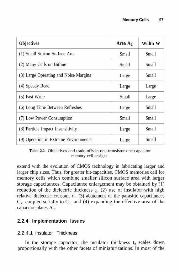
Memory Cells 97
Objectives Area AC Width W
(1) Small Silicon Surface Area Small Small
(2) Many Cells on Bitline Small Small
(3) Large Operating and Noise Margins Large Small
(4) Speedy Read Large Large
(5) Fast Write Small Large
(6) Long Time Between Refreshes Large Small
(7) Low Power Consumption Small Small
(8) Particle Impact Insensitivity Large Small
(9) Operation in Extreme Environments Large Small
Table 2.2. Objectives and trade-offs in one-transistor-one-capacitormemory cell designs.
extend with the evolution of CMOS technology in fabricating larger andlarger chip sizes. Thus, for greater bit-capacities, CMOS memories call formemory cells which combine smaller silicon surface area with largerstorage capacitances. Capacitance enlargement may be obtained by (1)reduction of the dielectric thickness td, (2) use of insulator with highrelative dielectric constant εd, (3) abatement of the parasitic capacitancesCld coupled serially to CS, and (4) expanding the effective area of thecapacitor plates AC.
2.2.4 Implementation Issues
2.2.4.1 Insulator Thickness
In the storage capacitor, the insulator thickness td scales downproportionally with the other facets of miniaturizations. In most of the
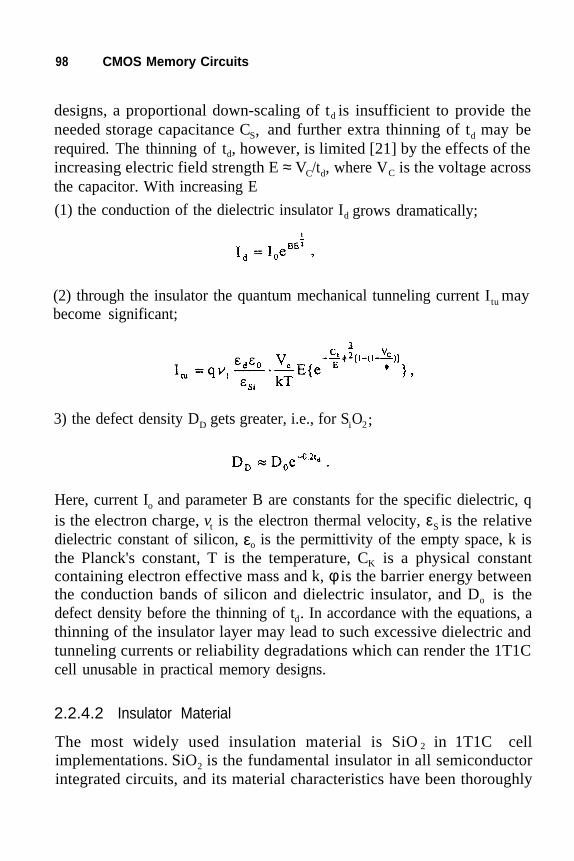
98 CMOS Memory Circuits
required. The thinning of td, however, is limited [21] by the effects of theincreasing electric field strength E ≈ VC/td, where VC is the voltage acrossthe capacitor. With increasing E
designs, a proportional down-scaling of td is insufficient to provide theneeded storage capacitance CS, and further extra thinning of td may be
(1) the conduction of the dielectric insulator Id grows dramatically;
(2) through the insulator the quantum mechanical tunneling current Itu maybecome significant;
3) the defect density DD gets greater, i.e., for SiO2;
Here, current Io and parameter B are constants for the specific dielectric, qis the electron charge, vt is the electron thermal velocity, εS is the relativedielectric constant of silicon, εo is the permittivity of the empty space, k isthe Planck's constant, T is the temperature, CK is a physical constantcontaining electron effective mass and k, φ is the barrier energy betweenthe conduction bands of silicon and dielectric insulator, and Do is thedefect density before the thinning of td. In accordance with the equations, athinning of the insulator layer may lead to such excessive dielectric andtunneling currents or reliability degradations which can render the 1T1Ccell unusable in practical memory designs.
2.2.4.2 Insulator Material
The most widely used insulation material is SiO 2 in 1T1C cellimplementations. SiO2 is the fundamental insulator in all semiconductorintegrated circuits, and its material characteristics have been thoroughly

Memory Cells 99
examined. SiO 2 is a paraelectric material, i.e., the displacement chargedensity D is linearly dependent on the external electric field E and inwhich no spontaneous polarization P occurs (Figure 2.6). If E0 and E 1 arethe electric field strengths generated by the voltages which in the binary
Figure 2.6. Displacement charge density versus external electric field in SiO2.
logic-system represent log.0 and log.1 respectively, then the chargeamount that differentiates the logic levels, i.e., the charge storage capacityof the 1T1C memory cell QC is
and the charge density on the capacitor Q'C is
where AC is the effective area of the storage capacitor plate and ∆D is thedifference in charge density. Increased Q'C may be obtained by theapplication of materials with higher εd than SiO2 has at a given E. Higher

100 CMOS Memory Circuits
εd and Q'C makes possible to reduce Ac and, thereby, the size of thememory cell. Size reductions by increases in εd, however, are limited bythe raises in currents IO and by the variations in material constant B (Table2.3). A raise in IO, or B, or in both IO and B, results in higher insulationconductivity Id and may appear as excessive leakage current through thedielectric material. Yet Ta2O5 dielectric insulation in 1T1C cells [22]seems to be attractive despite its very high IO and B. Si3N4 insulator has ahigh IO, a low B and a small improvement factor of 1.8 in εd in comparisonto SiO2. Popularly applied SiO2-Si3N4 combinative insulators exploit thehigher material integrity of Si3N4 to improve memory yield rather thantaking advantage of the elevated εd to increase capacitance per area. Otherparaelectric materials with high εd, e.g., Y2O3,ZrO2, etc., may also be appliedin 1T1C cells, but the emergence of ferroelectric insulators offers alsoattractive alternatives.
Material εεd Io B
SiO2 3.9 5.1 x 10 -28 17.7
Si3N4 7.0 9.2 x 10⁻¹⁸ 11.7
Ta2O5 23.0 4.1 x 10⁻¹⁵ 23.4
Table 2.3. Material parameters εd, Io and B of SiO2, Si3N4and Ta2O5 insulators. (Source [21])
Most of the CMOS-applicable ferroelectric materials [23] have aperovskite crystal structure described by the general chemical formulaABO3. Elements A and B are large and small cations respectively.This cation-oxide crystals possess pyroelectric, piezoelectric andferroelectric properties. Ferro-electricity means that the material possessesspontaneous electric polarization P that can be reversed by an appliedexternal electric field E. With P and E the displacement charge density Dcan be expressed as

Memory Cells 101
In the ferroelectrics, which are considered to use in 1T1C cells, P>> ε0Eand, therefore, D≈P. P as a function of E curves a hysteresis loop, and theP(E) curve is nearly identical with the D(E) curve (Figure 2.7). In thiscurve, E c is the coercive electric field where the net polarization reverses,
Figure 2.7. Polarization and displacement charge density versus external electricfield in a ferroelectric material.
E SAT and PSAT define the saturation point of the polarization, and Pr is theremanent spontaneous polarization that remains aligned with previouslyapplied E. With the slopes of the D(E) curve the εd is nearly proportional[24]; εd→∞ at EC, and εd →0 at ESAT. Furthermore εd rises to anomalouslyhigh values near the phase-transition temperature To (Figure 2.8). At thecharacteristic temperature To the material changes from fersoelectric phaseto paraelectric phase and from paraelectric phase to ferroelectric phase.Thus, the use of ferroelectric insulators to shrink 1T1C cell sizes can bebeneficial in both paraelectric and ferroelectric phases near To, if T o is

102 CMOS Memory Circuits
adequately chosen. To should be outside the operating temperaturerange of the memory so that the cell operates only in either para- orferroelectric phase. In ferroelectric state the charge storage density Q'Cmay be obtained from the hysteresis loop
Figure 2.8. Permittivity versus temperature. (Source [24].)
The hystereses in D(E) and P(E) curves are unintended to be used indynamically operating memory cells; merely the benefits of the high εd areexploited. In addition to high εd the insulator in a 1T1C memory cell has tosatisfy requirements in dielectric leakage-current, breakdown-voltage,defect-density and reliability including the effects of aging and fatigue;and the implementation of the high εd must be compatible with the CMOSprocess. A combination of CMOS-process compatibility and high εd maybe achieved, e.g., by the use barium-strontium-titanate compounds ascapacitor dielectric and platinum for capacitor plates [25]. Experimentalprocessing of memory cells using Pb,Zr,TiO3 (PZT); Pb,La,TiO3 (PLT);Pb,La,Zr,TiO 3 (PLZT); BaTiO3; Pb,Mg,NbO 3 (PMN); Pb,Mg,Nb,O3-PbTiO3 (PMNPT); SrTiO3 and other materials have also shown someencouraging results.

Memory Cells 103
2.2.4.3 Parasitic Capacitances
In the implementations of memory cells, the use of CMOS processingcauses to exist parasitic capacitances, which may significantly reduce theeffectiveness of the storage capacitors. Dynamic memories of moderate bitcapacities may use planar capacitors (Figure 2.9) in which the depletion
Figure 2.9. Storage and depletion layer capacitances in 1T1C memory cellsusing lightly doped (a) and heavily doped (b) silicon surface.

104 CMOS Memory Circuits
layer in the silicon forms a serial capacitance Cld with the storagecapacitance CS. To provide a reasonable Cld/Cs ≤0.05 the doping concen-tration Nd under the capacitor plate has to be adjusted. A doping adjust-ment may interfere with other facets of CMOS processing, such as thecontrol of junction breakdown and threshold voltages, and may beconstrained by the critical electric field ECR that causes impact ionization.Applying the dependency of ECR from N, a lower bound for dopingconcentration adjustment can be found [26] as
Here Vs is the voltage on Cs, εsi and εo is the permitivity of the silicon andvacuum respectively, and Ac is the surface area of the storage capacitor.Storage capacitors which are formed between a pair of polysilicon layers(Figure 2.10) make the design free from the constraint imposed on N.
Figure 2.10. Storage capacitance between polysilicon layers.

Memory Cells 105
2.2.4.4 Effective Capacitor Area
To increase the storage capacitance CS, the extension of the effectivearea of the capacitor plates AC has widely been used in CMOS memories.CMOS fabrication technologies allow to include processing steps to createtrenches in the silicon bulk, to stack polysilicon devices above transistorsand wirings, and to make coarse polysilicon surfaces. Making trench-capacitors (Figure 2.11) [27] seems to be a cost-effective approach; but an
Figure 2.11. Trench-capacitor structure. (Extracted from [27].)
increase in processing complexity is necessary to control the unevenoxide-growths and leakage currents at the surface of the trench. Thesephenomena in the vicinity of the trench are results of the various crystal-orientations (Figure 2.12) which occur due to the oval or circular shape ofthe trench on the silicon surface.

106 CMOS Memory Circuits
Figure 2.12. Crystal orientations along the contour of an actual trench-capacitor.
Stack capacitors can most effectively be formed between polysiliconlayers (Figure 2.13) [28], but the implementation of large capacitor platesabove the access transistor and wiring may require high-temperatureprocessing steps which effect the characteristics of the circuits placedunder the capacitor.
The effective surface of the capacitor plates may also be enlarged byshaping grains, textures or other forms of granuality [29] into the surfaceof the polysilicon storage nodes. Granulation, of course, is the mosteffective in extending capacitance when the layers can follow each other'ssurface shape (Figure 2.14).
The most efficient silicon surface utilization may be achieved bydesigning memory cells, which can be placed in the area determined bythe crossover of a minimum-width bitline and a minimum-width wordline,

Memory Cells 107
Figure 2.13. A stack capacitor formation. (Derived from [28].)
Figure 2.14. Granulation of polysilicon surface.

108 CMOS Memory Circuits
and in a distance from each other established by the metal-to-metalminimum spacing (Figure 2.15). Designs to approach this minimum cell-area require to place perpendicularly to the silicon surface both thecapacitor and the access transistor (Figure 2.16) [210,211]. Nevertheless,access devices formed on the surfaces of polysilicon slabs or of trenches insilicon-crystals may have characteristics which differ substantially fromthose of conventional CMOS transistors. Degradations in transistorparameters e.g., in drain-source and drain capacitances, subthresholddrain-source leakage currents, gain factors, and others, and interactionsamong neighbored transistors and capacitors may seriously constrain the
Figure 2.15. Efficient surface utilization.

Memory Cells 109
Figure 2.16. One-transistor-one-capacitor memory cell designs perpendicular tothe silicon surface. (Derived from [210] and [211].)
applicability of 1T1 C memory cells with structures perpendicular to thesilicon surface. Yet, the mitigation of these transistor-parameter degrada-tions is within the grasp of the CMOS technology, and the resultingimprovements further strengthens the dominance of ITIC cells in CMOSmemory designs.

110 CMOS Memory Circuits
2.3 DYNAMIC THREE-TRANSISTOR RANDOM ACCESSMEMORY CELL
2.3.1 Description
Three-transistor (3T) dynamic cells have applications in integratedcircuits which combine CMOS digital logic and memory functions, butthey are seldom used in designs of memory-only chips. 3T memory cellscan be implemented with inexpensive processing technologies which aredeveloped for fabrication of digital circuits, because their implementationdoes not require the use of sophisticated processing steps. In stackedconfiguration the circuit of a 3T memory cell may be designed in a siliconsurface area that is smaller than the area requirement of any static memorycell design, but larger than that of the 1T1C memory cell. Yet, memoriesusing 3T memory cells provide faster write and read operations than thoseapplying 1T1C memory cells. As a drawback, the data stored in 3Tmemory cells can easily be upset by the impacts of low-energy atomicparticles, because the storage capacitance in a 3T cell is usually smallerthan that in 1T1C cells.
In a 3T memory cell (Figure 2.17) [212] the capacitance CS on the gateof a transistor M1 stores an amount of charge that represents a binarydatum, another transistor M2 is devoted to write access only, and a thirdMOS device M3 facilitates the read access. At write, device M2 is turnedon and a write buffer charges or discharges CS through a write-bitline BW.Depending on what amount of charge and corresponding voltage is storedon CS transistor M1 stays either turned on or off when M2 is deactivated.At read M3 is activated, M2 remains in high-resistance state, and the readbitline BR is precharged to voltage VPR. V PR changes significantly if M1 ishighly conductive, and changes very little if M1 is in low conductancestate. During refresh operation first M2 is turned off and M3 is turned onto provide a signal for read-out. Upon amplification, M2 is turned on, andallows for rewrite a datum on the storage node of the memory cell. In theimplementations of this memory cell, the write-bitline capacitance CBW,the read-bitline capacitance CBR and the wordline capacitance CWL areusually significant and restrict speed and power parameters.

Memory Cells 111
Figure 2.17. A three-transistor memory cell circuit.
2.3.2 Brief Analysis
Write and read signals, which are generated in and by a 3T memorycell, may be characterized by exploiting the analogy between the 3Tmemory-cell operation and the charge and discharge of a capacitor Cthrough a resistor R. The time functions of charge vc(t) and discharge vd(t)signals on C through R are well known as
where Vo is the amplitude of the generator step-signal Vo1(t) and τ = RC.

112 CMOS Memory Circuits
In a 3T memory cell, for write operations
may be applied in the equations of vc (t) and vd(t), where VDD , VT and V BG
are the supply, threshold and backgate-bias voltages, RBW is the resistanceof the write-bitline BW,rd2(t) is the time-dependent drain-source resistanceof transistor M2, and cs(t) is the time-variant storage capacitance. Simi-larly, for read operations
may be used. Here, VPR and ∆v are the precharge and the memory-cellgenerated voltages, RBR is the read-bitline resistance, rd1(t) and rd3(t) are thetime-dependent drain-source resistances of transistors M1 and M3, andcBR(t) is the time-variant read-bitline capacitance, may be applied toapproach vc(t) and vd(t).
For plausibility studies, in the examinations of both write and readsignals all parameters rd1(t), rd2(t), rd3(t), cs(t) and cBR(t) may be replaced bytheir time-invariant counterparts rd1, rd2, r d3 , Cs and CBR. With time-invariant parameters in the equations of vc(t) and vd(t), a crudeapproximation formula for the rise- and fall-times of the charge and dis-
charge signals tr=tf=t=τ lnk can be obtained, where k is a constant.
The expression of t=tr=tf indicates that both fast write and readoperations are obtainable at the use of minimum size devices in a 3Tdynamic memory cell. Minimum size write and read access transistors M2and M3 lessen the parasitic capacitance of the write-bitline CBW, of theread bitline CBR and of the wordline CWL. The reduction of the storagecapacitance CS is limited mainly by the required single event upset ratemaximum, i.e., the required immunity for atomic particle impact of thememory (Section 5.3). In the memory cell, CS may be increased withoutthe size-expansion of device M1. Applications of minimum-size transistordevices within a 3T memory cell is important in improving bothoperational speed and packing density. Operational speed increases by the

Memory Cells 113
reduced capacitances CBW , CBR and CWL despite the effects of the largerresistances rd1 , r d2 and rd3 , while packing density increases by the reducedsurface area required for the constituent transistors. To further reducesurface area, 3T cells may be designed in stacked configurations, wherethe transistors are placed each above the other one (Section 2.2.4.4).
2.4 STATIC 6-TRANSISTOR RANDOM ACCESS MEMORYCELL
2.4.1 Static Full-Complementary Storage
Static 6-transistor (6T) full-complementary memory cells are appliedin memory designs to satisfy requirements for short access- and cycle-times, high frequency data rates, low power dissipation, radiationhardness, operation in space, high-temperature, noisy and other extremeenvironments. For the benefits in performance and environmentaltolerance 6T cells compromise cell-sizes and, thereby, packing densities.
Figure 2.18. A static six-transistor full-complementary memory cell.

114 CMOS Memory Circuits
Yet, packing densities obtainable by the use of 6T cells are considerablyhigher than packing densities achieved by other memory cells whichprovide the same performance and environmental tolerance as 6Tcomplementary memory cells do.
A static 6T complementary memory cell (Figure 2.18) latches a digitaldatum in a pair of cross-coupled CMOS inverters, which are formed of 4transistors, MN1, MN2, MP3 and MP4, and uses a pair of access devicesMA5 and MA6 to couple and decouple the storage latch to and from othercircuits. Both inverters in the latch as well as both access transistors areidentical, and the layout design of the cell is mirror-symmetrical.
The data storage capability of this memory cell rests on the wellknown fact that a pair of complementary inverters in positive-feedback, oras also called in latch, cross coupled, or Ecless-Jordan configuration, hastwo stable states. Positive feedback exist in the operation region of thiscircuit where both the low-frequency small-signal loop gain AL and thetotal phase-shift in the loop ρL fulfills the Barkhausen criteria [213](Section 3.3.4.2)
A L = A1 · A 2 = A² > 1,
ρL = ρ1 + ρ 2 = 2ρ= 2π ,
where A1 and A2 are the gains and ρ1 and ρ2 are the phase angles of the firstand second complementary inverters respectively. In a 6T memory cell thetwo inverters have approximately the same gain A ≈ A1 ≈ A2 and the samephase shift ρ ≈ ρ1≈ ρ2, therefore
Here, N and P subscripts indicate n- and p-channel devices respectively;gm is the transconductance and rd is the drain-source resistance of thedevices when the circuit operates in the vicinity of the metastable state orof the flipping point. Voltages representing the flipping point VF and bothstable states V1 and V2 can conveniently be determined by the use of thenormal v1 = f(v2) and mirrored v2 =g(v1) voltage transfer characteristics of

Memory Cells 115
the inverters (Figure 2.19). The voltage VF may also be defined by avariety of different methods comprising the application of the (1) closedloop unity gain, (2) zero Jacobian determinant of the Kirchoff equations,(3) coincidence of roots in flip-flop equations, and the (4) inverters'transfer characteristics.
Figure 2.19. Normal and mirror input-output voltage characteristicsof the inverters in a six-transistor cell.
In a pair of crosscoupled inverters the pair of the stored voltage levelsare able to return to and stay V1 and V2 as long as the amplitude of a latch-external signal ∆V on either one or both of the storage nodes and
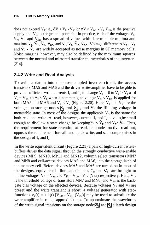
116 CMOS Memory Circuits
does not exceed VF i.e., ∆V < VF - VSS or ∆V > VDD - VF. V DD is the positivesupply and VSS is the ground potential. In practice, each of the voltages V1,V2, VF and VDD has a spread of values with determinable minima andmaxima and Voltage differencesand are widely accepted as noise margins in 6T memory cells.Noise margins, however, may also be defined by the maximum squaresbetween the normal and mirrored transfer characteristics of the inverters[214].
2.4.2 Write and Read Analysis
To write a datum into the cross-coupled inverter circuit, the accesstransistors MA5 and MA6 and the driver write-amplifier have to be able toprovide sufficient write currents I1 and I2 to change V1 = 0 to andV2 = V DD to when a common gate voltage is applied forboth MA5 and MA6 and V1 < V2 (Figure 2.20). Here, V1 and V2 are thevoltages on storage nodes and , and VF the flipping voltage inmetastable state. In most of the designs the applicable VG is the same forboth read and write. At read, however, currents I1 and I 2 have to be smallenough to disallow a state change by keeping and Thus,the requirement for state-retention at read, or nondestructive read-out,opposes the requirement for safe and quick write, and sets compromises inthe design of I1 and I2.
In the write equivalent circuit (Figure 2.21) a pair of high-current write-buffers drives the data signal through the strongly conductive write-enabledevices MP9, MN10, MP11 and MN12, column select transistors MN7and MN8 and cell-access devices MA5 and MA6, into the storage latch ofthe memory cell. Before devices MA5 and MA6 are turned on in most ofthe designs, equivalent bitline capacitances CB and are brought tobitline voltages VB = VSS and = VDD - VTN (VBG ) respectively. Here, VTN
is the threshold voltage of transistors MN7 and MN8, and VBG is the back-gate bias voltage on the effected devices. Because voltages VB and VB arepreset and the write transient is short, a voltage generator with step-functions vg(t) = ± 1(t) [VDD - VTN (VBG)] may be used to substitute thewrite-amplifier in rough approximations. To approximate the waveformsof the write-signal transients on the storage nodes and a latch design

Memory Cells 117
Figure 2.20. Access current and storage voltage changes versusaccess gate voltage variations.
with a flipping voltage VF=[VDD-VTN(VBG)]/2 may be assumed. This VF
divides the development of the signal amplitude on either storage nodeor into two regions. In the first region the generator or write-data signalworks against the effects of the positive feedback, in the second region thepositive feedback accelerates the signal development. Presuming that thetwo regions are nearly equal, then the signal acceleration and decelerationin the two regions can cancel each other, and the presence of positive feed-

118 CMOS Memory Circuits
Figure 2.21. Write equivalent circuit for an SRAM designedwith 6T memory cells.
back may be disregarded in a first order waveform-estimate model (Figure2.22). A transient analysis on this model yields the well-known exponen-tial waveform on node or (Section 2.2.2), and from that the write-

Memory Cells 119
Figure 2.22. Model circuit for first order estimation of write waveforms.
switching time tW, i.e., the fall time tfW and the rise time trW of the signalson nodes and may be approximated as
Here, VTA is the threshold voltage of the access transistors MA5 and MA6,rdP and rdN are the respective time-invariant equivalents of the time-dependent rdA(t), rdP(t) and rdN(t) drain-source resistances of the accessdevices MA5 and MA6, p-channel devices MP3 and MP4, and n-channeldevices MN1 and MN2; RB is the bitline resistance; and C is the time-S
invariant equivalent for the time dependent cS(t) storage node capacitance.
At read, first the capacitance of the bitline CB≈C is precharged to VPR,and then the bitline is disconnected from the other circuits except from theaccessed memory cell. After that CB≈C is charged or discharged throughthe bitline resistance RB and through the generator resistance RG of thememory cell. Most of the 6T cells are designed so that access transistorsMA5 and MA6 operate in the saturation region, and in each inverter one

120 CMOS Memory Circuits
device is turned on and operates in the triode region during the entire readoperation. Thus, the read-signal generated on the bitline B or mayconveniently be approximated by using a simple model (Figure 2.23). Asdiscussed previously the read-switching time tR, fall time t fR and rise timetrR can be obtained as
where, ∆VR is the read-signal swing on the bitline, rdSA is the drain-sourceon-resistance of the access device in the saturation region, rdtP and rdtN arethe drain-source on-resistances of the p- and n-channel transistors of theinverters in the triode region.
Figure 2.23. Model circuit for read-signal approximation.
The equations for switching times tW and tR clearly indicate that thedrain-source on-resistance of the access devices should be small for bothfast write and quick read operations. Nevertheless, a fast write requiressmall latch transistors which provide rather high drain-source resistances,while a quick read calls for wide latch-transistors with little drain-sourceon-resistances. Wide latch transistors improve operation and noise

Memory Cells 121
margins, radiation hardness and tolerance of other environmental affectsalso, up to the limitation imposed by increased drain-source leakagecurrents. Yet, any increase in any transistor size can expand the siliconsurface area of the memory cell, may oppose the conditions fornondestructive read-out, and a number of other design objectives.
2.4.3 Design Objectives and Concerns
The design of the constituent transistors of a 6T static memory cellshould approach objectives and satisfy contradictory requirements (Table2.4) which are similar to those of the 1T1C cell design (Section 2.2.3). Toapproach the objectives for a 6T cell the design can vary both the width Wand length L and, thereby, the aspect ratio W/L in the gain factor β of theindividual transistors. Principally, the quotient of the gain factorsβq = βA/βN ≈ βA/βP where indices A, N and P mark access, pull-down n-channel and pull-up p-channel transistors, have to be designed to assuresafe write and nondestructive read operations. Usually, a 6T cell designwith β q ≈0.35 allows for the use of a single gate voltage V G≈VDD on the
access transistors for both write and read functions. Facilitating conditionsfor safe and quick writes by VG > VDD is not recommended because ofincreased hot carrier emission, device-to-device leakage currents, eventualtransistor punch-through, instability and breakdown phenomena.Minimum transistor sizes with βq =1 may be designed at the application ofmidlevel precharge, low-current sense amplifier and high-current writeamplifiers. Application of a particular threshold voltage to the accesstransistors, that is higher than the threshold voltages of the othertransistors in the memory cell, is also a widely used method to circumventthe write-read paradox. Higher threshold voltages in the access transistorsresult in decreased subthreshold leakage currents and, thereupon, inincreased noise margins, and allow for higher number of memory cellsconnectable to a single bitline. The static noise margins in 6T memorycells can be designed by altering the transistor aspect ratios W/L-s and thedevice size ratios βq -s and, occasionally, by varying threshold voltages
and other device parameters.

122 CMOS Memory Circuits
Objectives Access LatchDevices Devices
(1) Small Surface Area Small Small
(2) Many Cells on a Bitline Small Small
(3) Large Operation Margins Small Large
(4) Nondestructive Read Small Large
(5) Speedy Read Large Large
(6) Fast Write Large Small
(7) Low Power Consumption Small Small
(8) Particle Impact Insensitivity Small Large
(9) Radiation Hardness Small Large
(10) Environmental Tolerance Small Large
Table 2.4. Objectives and requirements in transistor sizes.
2.4.4 Implementations
The silicon surface area of 6T memory cells, in planar designs, may beoverly large to meet objectives in packing density and performance for aprospective CMOS memory. To improve packing density and speedperformance, numerous CMOS processing technologies feature trench-isolation between p- and n-wells e.g., [215] and stacked transistorse.g., [216]. Stack transistor technology, in its most widely used form,places p-channel polysilicon thin-film transistors over n-channeltransistors which are implemented in silicon crystals (Figure 2.24). Inmany thin-film implementations the channel lengths of the transistors haveto be extended, and channel offsets have to be introduced, to decrease thesubthreshold leakage currents to a required limit, e.g., to 10-13 A/m.

Memory Cells 123
Furthermore, the nonlinear current-voltage characteristics of the parasiticdiode-like devices (Section 6.3.4), which may occur as a result ofcombining P+ and N+ doped materials at junctions of p- and n-channeltransistors, have to be considered in the circuit design. This and otherthree-dimensional designs of 6T memory cells, of course, requireincreased complexity in the CMOS fabrication technology. Nevertheless,the potential to provide large bit-capacity static memory chips, fastmemory operations and high manufacturing yields, exceedingly outweighsthe augmentation of the fabrication complexity.
Figure 2.24. Stack-transistor implementation. (Derived from [216].)
An increase in memory circuit complexity is also required for theapplication of static memory cells. Namely, in memory cells selected byan activated wordline and connected to unselected bitlines, the stored datamay be altered by the combined effects of the precharge voltage, couplednoises, and leakage currents of the memory cells connected to the samebitline. To avoid data scrambling in cells connected to the unselectedbitlines, the application of bitline loads are needed. These loads arecoupled to the bitlines when the precharge is completed (Figure 2.25). Inthis exemplary bitline-terminating circuit, the serially connected transistor

124 CMOS Memory Circuits
pairs MN9-MP11 and MN10-MP12 act as bitline load devices. MN13 andMN14 are the bitline-select or column-select transistors. TransistorsMN16 and MN17, in parallel configuration, determine the prechargevoltage VPR = V DD -VTN (VBG), and during precharge MP20 assists to equal-
Figure 2.25. A bitline terminating circuit.
ize the voltages on the bitlines B and . A precharge of B and occurswhen devices MP18, MP19 and MP20 are turned on by impulse φPR
simultaneously with the activation of MN13 and MN14 by bitline-selectimpulse φ . At the same time, in the unselected columns φY Y disallows theprecharge and data transfer, and connects load devices MN9, MN10,

Memory Cells 125
MP11 and MP12 to the unselected bitlines. The separation of the loadsfrom the selected bitline improves the sensing speed and the operationmargins, while the bitline selective precharge greatly reduces the powerdissipation of the memory and decreases the substrate currents and theemission of hot-carriers. Less hot-carrier emission results higher reliabilityin memory operations.
To provide fast read operations not only the sensing and read circuits,but also the precharge of the bitlines must be quick. Speedy prechargerequires high β with W/L >10 for devices MN16, MN17, MP18, MP19and MP20. Yet, minimum size load devices MN9, MN10, MP11 andMP12 may be sufficient to prohibit data alteration in the unselectedbitlines. Since in this circuit bitline-select transistors MN13 and MN14 arecoupled to the precharge devices and to the bitlines in series configuration,the β of the device pair MN13-MN14 should be about as large as the β oftransistors MP18 and MP19.
2.5 STATIC FOUR-TRANSISTOR-TWO-RESISTOR RANDOMACCESS MEMORY CELLS
2.5.1 Static Noncomplementary Storage
Static noncomplementary four-transistor-two-resistor (4T2R) memorycells are used in memory designs, typically in RAMs, to combine highpacking density with short access and cycle times and with simpleapplication in systems. Applications of 4T2R cells allow for obtainingmemory packing densities which are between those attainable by designsbased on dynamic 1T1C and static 6T memory cells, and which arecomparable with designs using dynamic 3T cells. The access and cycletimes of memories employing 4T2R cells, however, are much shorter thanthose obtainable with 1T1C cells and somewhat longer than thoseperformed by memories designed with 6T cells. For long-term data storage4T2R cells do not need refresh, but in the cells the stored data can be upsetby charged atomic particle impacts and by other various environmentaleffects with much higher probabilities than the data stored in 6T memorycells.

126 CMOS Memory Circuits
The static 4T2R memory cell (Figure 2.26) is a noncomplementaryvariation of the elementary circuits which use a symmetrical pair ofinverters in positive feedback configuration for storage, and a symmetricalpair of transmission devices for access. All active devices MN1, MN2,MA3 and MA4 are uniformly either n- or p-channel devices, and theinverters are implemented as transistor-resistor compounds MN1-R5 andMN2-R6.
Figure 2.26. A static four-transistor-two-resistor memory cell circuitwith leakage currents.

Memory Cells 127
Resistors R5 and R6 are applied, primarily, to avoid loss of data,i.e., compensate the effect of leakage currents I L1 and I L3 on node potentialVS, when both access devices MA3 and MA4 and one of the drivertransistors MN1 are turned off, and to balance I L2 and I L3 when MA3, MA4and MN2 are turned off. Here, I L1 + I L3 = I L2 + I L4 = I L is assumed. With IL
and with an allowable VS the maximum resistance R=R5=R6 can easily bedetermined. In practice, the maximum applicable resistance R, however, isgreatly influenced by ∆R which amounts the variations of R;
∆R = ∆R PT + ∆RT + ∆RE ,
where resistance-variations ∆R PT , ∆ R T and ∆R E are functions of theprocessing technology, temperature and environments including the effects
Figure 2.27. Specific resistance versus implant dose for furnaceand laser annealed polysilicon.

128 CMOS Memory Circuits
of radioactive radiation, humidity, and others. Usually resistor R isimplemented in polysilicon, and the influence of the CMOS processingtechnology, specifically the annealing-method, dominates the magnitudeof ∆R (Figure 2.27). A large ∆R, as it appears at furnace annealing, mayrender 4T2R cells unusable due to high standby currents and excessivememory power dissipation. High R, low power dissipation and large bitcapacity-per-chip can be obtained by processing improvements, e.g., bythe exploitation of laser technology, thermal cycling, etc., in the fabri-cation of 4T2R memory cells.
2.5.2 Design and Implementation
By all means, CMOS processing technologies should minimize drain-source leakage currents in all the transistors of a 4T2R memory cell. Yet,when either transistor pair MN1-MA3 or MN2-MA4 are off, the leakagecurrents must have certain ratios I L1 /I L3 and I L2 /I L4 to keep the storage nodeson potentials which provide adequate noise margins. I L1 / IL3 and I L2 /I L4 maybe altered by the variation of device sizes and, thereby, by the gain factorquotients β q = β 1 / β 3 = β 2 / β4 . In usual designs, β q <0.4 and a resistor currentIR ≤0.1I L are needed to keep the storage node of the deactivated access anddriver transistors on the required potential. These requirements in βq and I R
contradict the conditions for sufficient noise margins on the storage nodewhich is associated with the drain of a turned on transistor MN1 or MN2(Figure 2.28). The diagram shows that a βq >2 is required for an acceptablenoise margin, and that at higher cell-supply voltage V CC larger static noisemargin V NM is obtainable. To provide acceptable noise margins in both theon- and off-side of the 4T2R cell and to avoid paradoxical β q requisites,the threshold voltage of each driver transistor MN1 and MN2 are often sethigher than the threshold voltage of each access device MA3 and MA4.Subthreshold currents in MA3 and MA4, nonetheless, must be small toassure sufficient operation margins in the sense circuit (Section 3.1.3) andto allow the connection of a high number of memory cells to the samebitline.
In 4T2R memory cells R5 and R6 provide the functions of thep-channel devices MP5 and MP6 employed in 6T memory cells(Section 2.4), thus R = R 5 = R 6 = r dP = r dtP = r dsP may be used in the equa-

Memory Cells 129
Figure 2.28. Noise margin versus device-size ratio.
tions for AL , t rw , t rR and t fR . Because R is large in comparison to the drain-source on-resistance of devices MN1 and MN2, and because the invertersare mirror-symmetrical, the Barkhausen-criteria for positive feedback caneasily be satisfied. Furthermore, because the R-s are high, above theflipping voltage VF the effect of the positive feedback is little; and a smallwrite current can rapidly change the information content of the 4T2Rmemory-cell. During a write operation the low resistances of the write-buffer output and the access device connects parallel with R, and one ofthe drive transistor MN1 or MN2 is turned off. At a read operation the on-resistance of either transistor pair MN1-MA3 or MN2-MA4 alters theprecharge voltage and the current on one bitline significantly, andinsignificantly on the other bitline. The more significant change is rapidlysensed and amplified by the sense amplifier, and the datum stored in thememory cell remains unchanged.
Most of the 4T2R memory-cell designs use polysilicon load resistorsR5 and R6 and place them over the transistors [217] similarly to the three

130 CMOS Memory Circuits
dimensional design of the 6T memory cell (Section 2.4.4). This three-dimensional placement of constituent elements requires at least two, butmost often three, polysilicon layers. Conveniently, the third layer may beapplied to extend the storage node capacitances C1 and C2 . High C1 and C 2
decreases the inherent susceptibility of 4T2R cells for the effects ofcharged atomic particle impacts (Section 5.3).
The application of 4T2R memory cells in arrays necessitates the use ofload devices to prevent data-loss in the accessed cells which are tied tounselected bitlines. In the write-read equivalent circuit (Figure 2.29)bitline B and are coupled to load devices MN9 and MN10 and toprecharge devices MN16, MN17, MP18, MP19 and MP20. TransistorsMN13 and MN14 provide bitline selection, MN7 and MN8 are applied forwrite enable and the other transistors and the two resistors represent the4T2R cell.
Traditionally, 4T2R memory cells can be designed to occupyconsiderably smaller silicon surface area and to perform faster writeoperations than 6T memory cells do. Nevertheless, three issues, (1)stacked device configuration, (2) single event upset rates, and (3) noisemargin considerations, may dwindle the size advantage and, somewhat,the write-speed benefits of the 4T2R cell over the 6T cell. In stackeddevice configuration, both the 4T2R and 6T cells may be designed to takeapproximately the same area (Section 2.4.4). Furthermore, the arearequirements for the 4T2R memory cells may be increased to satisfyrequirements in single event upset rates by enlarging storage-nodecapacitances (Section 5.3.3), and to provide 6T-cell-equivalent noisemargins by augmenting the device-size ratios. 4T2R memory cells areprone to the effects of atomic particle impacts, because of their inherentlysmall capacitances and large load resistances. Large load resistancesreduce the achievable highest voltage on the cell node, and the reductionmakes also the noise margin for log. 1 smaller.

Memory Cells 131
Figure 2.29. Write-read equivalent circuit in an SRAM designedwith 4T2R memory cells.

132 CMOS Memory Circuits
2.6 READ-ONLY MEMORY CELLS
2.6.1 Read-Only Storage
In a read-only memory (ROM) cell, data can be written only one time,the one-time writing or programming is a part of the fabrication process,the cell holds a datum for its life-time and can be read arbitrary timesduring its life-time. (As contrasts, in so-called programmable read onlymemory PROM cells, the stored data can be determined by the end-user,and with the exception of fuse and antifuse cells, PROM cells may beprogrammed more than once.) ROM cells may be applied in all randomaccess, sequential and content addressable memory designs. Yet, in thecommon use, the denomination ROM implies random access operation,and eventual other access modes are expressed by added attributes,e.g., sequential ROM, content addressable ROM. Commonly, ROM-cellsare employed in control and process program stores, look-up tables,function generators, templates, knowledge bases, etc., and in generalimplementations of Boolean and sequential logic circuits. Most ROM cellsused in CMOS memories operate in binary logic system, but an increasingnumber of CMOS ROMs exploits the benefits multiple-valued nonbinarymemory cells.
A ROM cell [218] in CMOS technology is as simple as a single n- orp-channel transistor. In the one-transistor (1T) ROM cell the gate of thetransistor serves as the control electrode of an access device, and the singletransistor combines both access and storage functions. To binaryapplications, the transistor can be programmed to provide either apermanently open circuit in NOR configuration (Figure 2.30), or apermanently low-resistance circuit in NAND configuration (Figure 2.31).In both configurations, transistors MPi and MPj are applied for pre-charging and for compensating leakage currents, or for forming resistiveloads in the NOR and NAND arrays. A NOR array of n-channel ROMcells requires a high voltage, e.g., the supply voltage V DD, to select awordline, e.g. Wi , while all other wordlines are kept at ground potentialVSS =OV. The selected W i turns all effected unprogrammed transistors on,but the programmed ones provide very high resistances between thebitline, e.g. Bi , and VSS . As results, the bitline Bi with the programmed cell

Memory Cells 133
Figure 2.30. Read-only-memory cells in NOR configuration.
remains on high voltage, e.g., V P R ≈ V DD , and bitlines with unprogrammedcells get discharged toward VSS. In NAND arrays of n-channel ROM cellsthe selected wordline Wi is brought to a low potential, e.g., V SS, and all theunselected wordlines remain on a high potential, e.g., VPR. The selected W i
turns the unprogrammed transistors off, while all other cells have lowdrain-source resistances. Thus, the potential of the bitline Bi , that iscoupled to a programmed cell, switches to VSS from V PR , while bitlineswith unprogrammed cells hold a high potential. This high potential mayconsiderably be less than VPR due to charge redistributions which mayplague precharged NAND configurations (Section 2.7.2).

134 CMOS Memory Circuits
Figure 2.31. Read-only-memory cells in NAND arrangement.
2.6.2 Programming and Design
In both NOR and NAND type of arrays the ROM cells may beprogrammed by varying the threshold voltage VT of the transistor in thecell. Conveniently, VT may be programmed by implanting different iondoses into the channel regions, or by altering the oxide thickness above thechannels. Moreover, oxide isolation between the bitline and the transistor-drain may also be used to program open circuits in NOR type of arrays.The choice among the various programming methods is based on theimportance of such requirements as highly reliable operation, high yield,and the possibility of programming in the final phases of the CMOS

Memory Cells 135
fabrication process. Programming near the end of the processing allowsdelivery of ROMs in short turn-around times.
The 1T ROM cell can also be programmed to store data in multi-levelforms by using a multiplicity of threshold voltages. Multiple-level circuitshave much smaller operating and noise margins than binary circuits do.Nevertheless, the development of sense circuits to detect signals with verysmall amplitudes (Sections 3.3-3.5) and improvements in processingtechnologies to decrease variations in threshold voltages and in otherparameters, make designs with multi-level ROM-cells feasible. A four-level ROM storage e.g., needs three threshold voltages V T1 , V T2 and VT3
which can be programmed in three ranges ∆V T1, ∆V T2 and ∆VT3 in practice(Figure 2.32). ∆V T1 divides the voltage region V R = V DD - V SS into anupper and a lower part, while ∆V T2 and ∆V T3 , subdivide each of both partsinto upper and lower parts too. At read, the stored datum is compared to∆ VT1 first, and then either to ∆V T2 or to ∆V T3 depending on the outcome ofthe first comparison. For the level comparison, either three senseamplifiers or one sense amplifier with three switchable reference levels, orthree precharge voltages, or a combination of these techniques, can beused. A variety of level-detection techniques may be borrowed fromanalog-to-digital A-D converter circuits [219].
Figure 2.32. Threshold voltage ranges for four-level ROM storage.

136 CMOS Memory Circuits
1T ROM cell based circuits may be analyzed and designed by theapparatus and methods used for random access memory cells (Section 2.2)and sense circuits (Section 3.1). ROM circuits designed in NOR config-urations result in faster read operations than ROMS designed in NANDconfigurations, because the bitline capacitance is charged and dischargedthrough single transistors which have zero back gate bias. Furthermore, thelack of charge redistribution in NOR arrays provide large operation mar-gins. This, in addition to operation capabilities in extreme environments,makes the 1T ROM cells in NOR-arrays more amenable to multi-levelstorage than the 1T ROM cells in NAND configurations. Implementationsof NAND arrays, however, require only one contact on a bitline and, inturn, may require less semiconductor surface area than NOR arrays formedof 1T ROM cells do. Because in CMOS applications 1T ROM cells can bedesigned to occupy smaller size and to provide faster operations than anyother ROM cells do, most of the CMOS ROM designs use 1T ROM cells.
2.7 SHIFT-REGISTER CELLS
2.7.1 Data Shifting
Shift-register cells are applied in sequentially accessed memories toprovide very fast write and read data rates. Fast shift register operations,however, are obtained at the expense of high power dissipations and lowmemory packing densities. Shift registers move the entire data content ofthe activated array from the inputs to the outputs, and each addresseddatum or data set has a unique time delay from a reference time point. Tostore and transfer data, a shift register cell (Section 1.3.3) requires controlsignal with two distinct phases, two access or transmission devices, twostorage elements and, eventually, two amplifying components in a singleshift register cell (Figure 2.33).
During a first phase, transmission device TR1 is brought to conductivestate by impulse φ1 and TR1 transfers a binary datum into the first storageelement SE1. The signal that represents a datum may be attenuated by thetransfer, and a signal amplifier A1 can be applied to recover the datum fora consequent shift. Furthermore, A1 ensures the direction of the data

Memory Cells 137
Figure 2.33. Generic shift-register cell composition.
shift by providing a forward amplification Af>>1 and a reverse amplifi-cation Ar<<1. For the time of a first data transfer, storage and ampli-fication, transmission device TR2 is turned off. In a second phase, impulseφ2 turns TR2 on, and impulse φ1 deactivates TR1. Thus, TR1 separatesstorage and amplifying elements SE1 and Al from the preceding stage,and the datum stored in SE1 is transferred through A1 and TR2 to storageelement SE2 and amplifier A2. Circuit complexes TR1-SE1-A1 andTR2-SE2-A2 are considered as the two halves of a single shift registerstage or shift register cell.
The structure and the operation of a shift register indicate threeimportant issues. (1) The load on the output of each half-cell is minimum(Fanout = 1) resulting in very quick data shifts. (2) One half of all shift-register cells are activated at each phase of the operation, which results invery high power dissipation. (3) Shift operations in an N-bit array need 2Naccess and 2N storage elements and, thereby, limit packing densities.Although amplifying elements are used in each half of a shift register cell,their applications are necessary only in those cells in which the signaldegradations reduce the noise margins to magnitudes unacceptable formemory operations.
Fast sequential, buffer and specialty memories, e.g., FIFOs, LIFOs,register-files and nonparallel associative memories, benefit mostly fromdesigns with shift-register cells. Random access and specialty memorydesigns also employ shift registers as supplemental circuits, e.g., in signalmultiplexers, parallel-serial and serial-parallel converters and timinggenerators. In serially accessed memories the use of shift-register cells islimited to rather moderate bit-capacities by the excessive power

138 CMOS Memory Circuits
dissipation P. P increases with the operating frequency f, total charged anddischarged capacitance C, and voltage swing V, i.e., P = fCV2 ; andimposes restrictions in operation speed and in packing density. Never-theless, extremely low power dissipation and very high operational speedat high packing densities can be combined by the use of shift-register cellsin shuffle memories (Section 1.3.4). Shuffle memory designs allow forcharge and discharge only of diminutive fractions of the total arraycapacitance, and apply only a half shift-register cell, or a single memorycell per bit for both data-move and data-storage.
CMOS implementations of shift-register cells may exploit theavailability of both n- and p-channel devices, and the very large input andout-put-off resistances of the MOS transistors. The alternating use of n-and p-channel transistors as transmission gates, eliminates the need fortwo separate wires to deliver two separate clock impulses to each shiftregister cell. Signal changes in the cells can be very fast, due to the full-complementary operation of the inverters and due to the small loadcapacitances. In many cases, the parasitic capacitances can be used astemporary data storage elements. Depending on the data storagemechanism CMOS shift-register cells, like the random access memorycells, may be of dynamic or static types.
2.7.2 Dynamic Shift-Register Cells.
In the widely applied CMOS dynamic six-transistor shift-register (6TSR) cell (Figure 2.34), the transmission devices are formed of a single n-and a single p-channel transistor, the data are stored in the inputcapacitances CS1 and CS2 of the CMOS of inverters, and the invertersamplify the signal amplitude to V=VDD -VSS . For convenience theamplitude of the clock signal Vφ is set Vφ =VDD . By using this Vφ , the data-signal amplitude V gets reduced by the threshold voltage VTN (VBG ) of then-channel device MN1 or by the threshold voltage VTP (VBG ) of thep-channel transistor MP4. Here, VDD , VSS and VBG are the supply, groundand backgate bias voltages. The reduced V results in slower operation.Furthermore, both the operational speed and the power dissipation areunfavorably effected by the one-clock two-phase operation that allows

Memory Cells 139
direct-current paths between VDD and VSS during the transient times ofclock signal φ.
Figure 2.34. A dynamic six-transistor shift-register cell.
By the application of two clocks φ1 and φ2 with a voltage amplitudeV φ = V φ l = V φ 2 > V DD + V TN (V BG ) , and by the use of uniform n-channeltransmission devices MN1 and MN4 (Figure 2.35), both the operationalspeed and power consumption can be improved. The control of thetransmission devices by two distinct clock signals reduces significantly thetime when a direct-current path may appear between VDD and VSS , whilethe elevated clock signal amplitude VDD + VTN (VBG ) allows to drive theinverters by a full voltage swing Vφ = VDD - VSS .
To obtain full voltage swings on the inverter inputs at the use ofp-channel transmission devices, a more negative Vφ than VSS is needed;Vφ <VSS - VTP (VBG ) . The generation of such negative Vφ requires the appli-cation of an extra isolated n-type well in the substrate, and that is usuallycost prohibitive for shift register implementations.

140 CMOS Memory Circuits
Figure 2.35. A two-phase dynamic shift-register cell.
The dynamic eight-transistor shift-register 8T SR cell (Figure 2.36)provides very high speed operation without the need for elevated voltagesfor clock impulses. No threshold voltage drop appears in this circuit, sinceboth the transmission devices MN1-MP2 and MN5-MP6 and the invertertransistors MN3-MP4 and MN7-MP8 are complementary pairs. Further-more, the full voltage swings which occur on storage capacitors CS1 andCS2 , degrade very little, because in this circuit configuration the effect ofthe charge redistribution is minimal.
Charge distributions may significantly reduce data signal amplitudes ina formally different but functionally equivalent half shift-register cell(Figure 2.37) where the transmission gates MN1 and MP2 are connectedto the power supply poles VCC and V SS . At the time to , devices MN1 andMP2 are turned on by impulse φ and φ,–
and the voltage vC1(t) on capacitorCS1 is vC1 (t o ) = VSS. At t1, the voltage vC2(t) on capacitor CS2 raises tovc2 (t ) = V . At t , voltage v (t) is switched to v , device MN31 DD 2 c1 c1(t 2) = VDD
is turned on, and all other transistors are in high impedance state. Between

Memory Cells 141
Figure 2.36. A high-speed eight-transistor shift-register cell.
Figure 2.37. Charge distribution effect in a half shift-register cell circuit.

142 CMOS Memory Circuits
t2 and t3 , the highly conductive MN3 allows a charge redistribution oncapacitors CS2 and CN , and at t 3 the voltage vC2(t) reduces to
Similar voltage swing degradation may occur due to the chargeredistribution on capacitor CS2 and Cp.
In the dynamic four-transistor-two-diode shift-register (4T 2D) SR cell[220] (Figure 2.38) both the charge redistribution and the directconductance between supply poles are avoided by the application of twopairs of control impulses φ1 - φ2 and φ3 - φ4 . All the four control signals φ1 ,φ2 , φ3 and φ4 can easily be generated from a common system clock φ. At adata shift operation, φ1 charges CS2 to Vφ = VDD through diode D3 if CS1
stores a low voltage VS1 < V TN , or through devices MN1, MN2 and D3 ifC S1 is on a high potential VS 1 >> VTN . Simultaneously, parasitic capacitanceCN is also charged to Vφ=VCC , because clock φ2 turns transistor MN2 on.Both transistors MN1 and MN2 are conductive after the appearance ofimpulse φ1 if VS1 > VTN, thus MN1 and MN2 discharges both CS 2 and C N .If VS1 < VTN , then both capacitances CS 2 and CN remain charged toVφ = VDD , because transistor MN1 is turned off and diode D3 is reversebiased. The other half of the cell MN4, MN5 and D6 is controlled byclocks φ3 and φ4 , and operates as described for the half-cell MN1, MN2and D3. For the implementation of diodes D3 and D6, CMOS processingtechnology is required. At some compromise in shifting speed, MOSdevices may replace the diodes.
All dynamically operating CMOS shift-register cells store data oncapacitors in forms of charge pockets. Due to leakage currents the amountof stored charges change, and the voltages which represent data, getcorrupted (Section 2.2.1). To prevent data degradation or loss, dynamicshift-registers must operate faster than a minimum shifting rate, and duringa long term data storage the information stored in the cells must beperiodically refreshed. The required time period for refresh may becalculated with the method described for dynamic random-access memorycells. Refresh operations in shift-register based memories are very simple,

Memory Cells 143
by connecting the input and the output of a shift register the stored datacan completely be recycled during the storage time and also at write andread operations.
Figure 2.38. High-speed dynamic shift-register cell with diodes. (After [220].)
2.7.3 Static Shift-Register Cells
CMOS static shift register cells can combine permanent data storage,without requirements for data-recycling, with very high speed data-shiftoperations. Seven-transistor static shift register (7T SR) cells (Figure 2.39)

144 CMOS Memory Circuits
Figure 2.39. Static seven-transistor shift-register cells.
employ a single feedback transistor MP7 or MN7 to form a data latch withdevices MN2, MP3, MP4/MN4, MN5 and MP6. When the feedbackdevice MP7 or MN7 is turned off, the 7T SR cells operate as dynamicshift-register stages do. When MP7 or MN7 is brought to a highlyconductive state by clock φ or φS, 7T SR cells store the data in the cross-coupled inverters permanently.

Memory Cells 145
If permanent data storage in each half-cell is required, the number oftransistors per shift-register stage has to be increased. A twelve-transistorshift register 12T SR cell (Figure 2.40) corresponds to two cascaded 6Trandom access memory cells. In this 12T SR cell, transmission gates MP6
Figure 2.40. A static twelve-transistor shift-register cell.
and MP12 make the link for positive feedback when devices MN1 andMN7 are turned off by clock signals φ1 and φ2 . Feedback devices MP6 andMP12 may be replaced by resistors R6 and R12, as it is exemplified in theten-transistor-two-resistor shift register 10T2R SR cell (Figure 2.41).Here, the higher the resistances R6 and R12 are, the faster the data shiftoperation is. Yet, in this shift-register cell the maximum resistance for R6and R12 is limited by the required immunity against the effects of atomicparticle impacts (Section 5.3) and by the leakage currents flowing throughdevices MN1 and MN7. Here, the alternating application of n- and p-channel transistors, rather than n-channel transistors only, as transmissiongates MN1 and MN7, makes possible to use a single clock φ for two-phasecontrol. The use of a single control clock and resistive feedbacks allows

146 CMOS Memory Circuits
for 10T2R SR cell designs which require considerably smaller siliconsurface area than 12T SR cell designs need.
Figure 2.41. Static shift-register cell with feedback resistors.
For the analyses, designs and implementations of the dynamic andstatic shift register cells described here, the techniques which are presentedin the discussion of the dynamic and static random-access memory cells(Section 2.2-2.5) can be adopted.
2.8 CONTENT ADDRESSABLE MEMORY CELLS
2.8.1 Associative Access
Content addressable memory (CAM) or associative access cells are thefundamental elements of all-parallel associative memories, and of manycache and other data-associative memory devices. Memories using CAMcells feature very fast operation in comparing an arbitrary data-word, or adata-set in a word, to a multiplicity of data-words or sets, in findingidentical or similar data-words or sets, in determining their addressinformation, and in establishing the degree of similarity. Random addressmemory (RAM) cells, however, occupy much less semiconductor surfacearea than CAM cell implementations do. Thus, the application of RAMcells are preferred in designs where the requirements for the time of the

Memory Cells 147
associative data search is noncritical, e.g., in word-parallel-bit-serial andbit-serial-word-parallel CAMs.
A CMOS CAM-cell combines a complete RAM cell with a one-bit digitalcomparator stage (Figure 2.42). The RAM cell includes a storage and oneor more access elements, and the digital comparator comprises logic gates
Figure 2.42. Content-addressable-memory cell structure.
that can provide an XAND, XOR, XNOR or XNAND function. To thelogic gate, the input variables are the true and the complement values of anargument datum B and and the true and the complement values of the
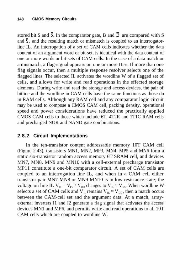
148 CMOS Memory Circuits
stored bit S and . In the comparator gate, B and are compared with Sand , and the resulting match or mismatch is coupled to an interrogator-line IL. An interrogation of a set of CAM cells indicates whether the datacontent of an argument word or bit-set, is identical with the data content ofone or more words or bit-sets of CAM cells. In the case of a data match ora mismatch, a flag-signal appears on one or more IL-s. If more than oneflag signals occur, then a multiple response resolver selects one of theflagged lines. The selected IL activates the wordline W of a flagged set ofcells, and allows for write and read operations in the effected storageelements. During write and read the storage and access devices, the pair ofbitline and the wordline in CAM cells have the same functions as those doin RAM cells. Although any RAM cell and any comparator logic circuitmay be used to compose a CMOS CAM cell, packing density, operationalspeed and power considerations have reduced the practically appliedCMOS CAM cells to those which include 6T, 4T2R and 1T1C RAM cellsand precharged NOR and NAND gate combinations.
2.8.2 Circuit Implementations
In the ten-transistor content addressable memory 10T CAM cell(Figure 2.43), transistors MN1, MN2, MP3, MN4, MP5 and MN6 form astatic six-transistor random access memory 6T SRAM cell, and devicesMN7, MN8, MN9 and MN10 with a cell-external precharge transistorMP11 constitute a one-bit comparator circuit. A set of CAM cells arecoupled to an interrogation line IL, and when in a CAM cell eithertransistor pair MN7-MN8 or MN9-MN10 is in low-resistance state; thevoltage on line IL VIL = VPR ≈VDD changes to VIL ≈ VSS. When wordline Wselects a set of CAM cells and V , then a match occursIL remains VIL ≈ VDD
between the CAM-cell set and the argument data. At a match, array-external inverters I1 and I2 generate a flag signal that activates the accessdevices MN1 and MP6, and permits write and read operations to all 10TCAM cells which are coupled to wordline W.

Memory Cells 149
Figure 2.43. A ten-transistor content-addressable memory cell circuit.
In an eight-transistor-two-resistor 8T2R CAM cell [221] the p-channeldevices MP3 and MP5 of the cross-coupled inverters are replaced by a pairof resistors R3 and R5 (Section 2.5). Resistive loads, rather than activeloads, may allow for cost reduction in manufacturing but degrades readperformance and environmental tolerance including the immunity againstthe effects of high temperature, atomic particle impacts and radioactiveradiation.

150 CMOS Memory Circuits
Operational speed and environmental tolerance are traded for benefitsin packing density and manufacturing costs in the four-transistor-two-capacitor 4T2C CAM cell (Figure 2.44) [222]. In this CAM cell transistor-capacitor pairs MN1-C2 and MN3-C4 form two dynamic one-transistor-one-capacitor 1T1C RAM cells (Section 2.3), and devices MN5 and MN6in combination with the cell- and array-external precharge transistor MP7and drive inverters I1 and I2 make up a one-bit comparator. Cell- andarray-external inverters shape the comparator signals, and provide the flag-signal that indicates a match between the data content of the argumentregister and the data stored in a set of 4T2R CAM cells.
Figure 2.44. A dynamic content-addressable-memory cell. (After [213].)
The detailed operation, analysis, design and implementations of CAMcells are obtainable from those discussed previously for random accessmemory cells (Section 2.2-2.5) and from the theory and design of CMOSlogic circuits.

Memory Cells 151
CMOS 10T CAM cell based circuits are applied mostly in space andmilitary equipment to implement other than traditional Von Neumann typeof computing systems, which have to operate with high computationalspeed in extreme environments. For operations in less severeenvironments, designs using 8T2R CAM cells are cost-effectivealternatives. In the future, the 4T2C CAM cells and similar small CAMcells have great potential to satisfy the need for high-packing-density low-cost CMOS components in the increasing number of nontraditionalcomputing systems. For special computations, of course, a diversity ofspecial CAM cells may be devised by combining a RAM cell with asimple logic circuit, e.g., [223].
2.9 OTHER MEMORY CELLS
2.9.1 Considerations for Uses
An abundance of memory cells may be devised to optimize designs forspecific combinations of requirements in speed, power and environmentaltolerance and to overcome limitations dictated by an available CMOSprocessing technology. Yet, CMOS compatible memory cells, which canbe implemented only at deviations from the main-stream fabricationtechnology, are very seldom or never used, regardless of their potentiallyoutstanding features. Furthermore, memory cells, which includenonstandard design features, but can be fabricated without any change inthe processing technology, are also infrequently applied to CMOSmemory designs. Namely, a divergence from either of both the main-stream CMOS processings and the memory cell designs, may result inexpansion of manufacturing costs, risks, and time-to-market of a memoryproduct. For stimulation of creative memory designs, however, a ratherarbitrary selection of memory cells, which are compatible with CMOStechnologies, are very briefly introduced in this section.
Innovations and research works in memory-cell technology aredirected to improve memory packing density, performance andenvironmental tolerance. Revolutionary memory cells may result in broadchanges in the semiconductor technology. Most likely, however, the main-stream CMOS memory technology will apply predominantly 1T1C and 6T

152 CMOS Memory Circuits
memory cells also in the foreseeable future, while an increasing share ofmemory designs will use nonvolatile memory elements.
2.9.2 Tunnel-Diode Based Memory Cells
Tunneling or delta-doped diodes applied as storage elements [224] cancombine very fast operation, capability to function in high-temperatureand radiation-hardened environments, very high packing density and staticdata storage. Tunnel diode based CMOS memory cells (Figure 2.45) storedata by using stable quiescent operation points, e.g., and , in the two
Figure 2.45. Tunnel-diode based memory cells. (After [224].)
positive-resistance regions of the current-voltage I-V characteristics of thediode D2 (Figure 2.46). A quiescent operating point, that occurs in thenegative-resistance region of the I-V curve, e.g., (San incremental raise of voltage across the diode reduces the current
3), is unstable, because
through the diode, and a voltage decrease enlarges the current. To providebistable storage in diode D2, the resistance of the load device R3 or MP3has to be fitted into a rather small domain. Access device MN1 must beable to provide sufficient diode currents, i.e., I2 > I p at Vp, and I 2 < Iv at VV,

Memory Cells 153
to flip the circuit from one stable state to the other one. Here, Ip and I v arepeak and valley currents, V are peak and valley voltages in thep and Vv
diode I-V characteristics. Resonant tunnel diodes [225] may exhibit more
Figure 2.46. Current-voltage characteristics and load curves for a tunnel-diode.
than one negative resistance regions (Figure 2.47) which make possible formulti level data storage. In memory cells which apply tunnel diodes, datacan be switched very quickly because the negative resistance greatlyreduces the time constant that appears by the operation of the memory cell
τ c (Section 2.2.2) in the memory cell. Moreover, these memory cells areinherently amenable to operate in high temperature and radiation environ-ments, since tunnel diodes are implemented in highly doped material andthe percentage change in the doping concentration of the tunnel diodes islittle in extreme environments. Sizes of tunnel-diode based cells may becompetitive with the sizes of dynamic one-transistor-one-capacitor cells.Namely, the load and diode devices can readily be placed under and abovethe access transistor by the exploitation of the technologies which areavailable for dynamic and static RAM-cell fabrications. Memory cells

154 CMOS Memory Circuits
using tunnel diodes do not need data refresh, but may require considerablestand-by currents for static data storage. Eventual cell current reductionsare limited by the diode-parameters Ip, Iv, Vp
and V , as well as by thev
required noise margins requirements, load-device characteristics and sensecircuit operations.
Figure 2.47. Current-voltage characteristics of a resonant tunnel-diode.(After [225].)
2.9.3 Charge Coupled Device
Charge couple device (CCD) based CMOS sequential memories canbe implemented in very high packing densities and perform high input andoutput data rates. CCDs, e.g., [226], store data as minority-carrier chargepockets in potential wells under the gate electrodes of MOS devices in thesemiconductor material (Figure 2.48). The potential wells are created bythe electric fields of the gates, and the strength and contour of the electricfields can be controlled by clock impulses brought on the gates. A mini-mum of two clocks φ1 and φ2 makes possible to move the charge pocketsalong the semiconductor surface, similarly to the operation of shift-registers (Section 1.3.3). A CCD cell needs very little semiconductor

Memory Cells 155
area because only two overlapping gates and no drain, source and contactare required for its implementation. The lack of drain and sourceelectrodes reduces parasitic capacitances and provides fast shiftingoperation. To facilitate shifting operation, nevertheless, all gates in theentire CCD memory have to be charged and discharged by impulses φ and1
φ within a single shift period, which results high operating power consump-2
Figure 2.48. A charge-coupled-device structure.
tion. In CCDs data have to be periodically refreshed, and downscaling offeature sizes increase the susceptibility of the stored data for the effects ofatomic particle impacts. Furthermore, the effects of charge trapping atinterface states, parasitic diffusion and drift currents result in incompletetransfer of minority carriers from well to well. The transfer efficiency η isthe fraction of charge transferred from one potential well to the next one

156 CMOS Memory Circuits
where Q i and Q i+1 are the charge amounts in well i and in well i+1, and ε isthe transfer inefficiency. Transfer efficiencies set the limit for the numberof CCD stages that may be cascaded without amplification, and they tendto decrease with increasing clock frequencies. Operations at higherfrequencies [227] may be facilitated by injecting a trickle charge (fat zero)to keep fast interface traps filled, by using a substrate with <100> crystalorientation, low doping concentration and buried channels to reduce thenumber of interface traps, by constructing potential slope inside each wellto propagate charge by built-in fields rather than by thermal diffusion.Thermally generated background charges cause spurious channel currents(dark currents) and, thereby, further restrains in speed and powerperformances. Nonetheless, very high speed CCD operations can becombined with extremely low power dissipations and with utmost packingdensities by applying CCD cells in a shuffle like-memory schema (Section1.3.4).
2.9.4 Multiport Memory Cells
Multiport memory-cells are employed to accommodate simultaneousor parallel write and read operations. Parallelism in computing and dataprocessing system greatly increases the data throughput rate. Multiportmemory cells [228] which stores a single datum, may include two or moreaccess devices MA1-MA4. The access devices may be connected toseparate write-bitlines BW1 and BW2, read-bitlines BR1 and BR2, write-wordlines WW1 and WW2 and read-wordlines WR1 and WR2 (Figure2.49a). Furthermore, multiport cells may comprise also a write-enabledevice ME1 that is controlled through a write-enable line WE1 (Figure2.49b), and may feature a cell-internal read amplifier AR in addition to astorage element SE (Figure 2.49c). In most of the multiport memory-celldesigns, traditional dynamic or static storage elements and transmissiongate type of access devices are employed (Section 2.3-2.5). Implemen-tations of multiple access memory cells result in large cell sizes, but manysystems, e.g., multiprocessor, superscalar, and graphic systems, do notrequire the use of very high bit-capacity multiport memories.

Memory Cells 157
Figure 2.49. Multiport memory cells.

158 CMOS Memory Circuits
2.9.5 Derivative Memory Cells
Clearly, the dynamic 1T1C, the static 6T and 4T2R memory cells arethe mostly applied elements to all random, sequential and special accessmemory designs. The 1T read-only memory cell looks to be the exclusivechoice for fixed program memories. High-speed sequential memorydesigns prefer the use of dynamic 6T or 8T shift-register cells. Apart fromthe main-stream demands, memory designs may need to satisfy somespecific circuit and process technological requirements. Specific designobjectives may justify the use of derivative or innovative memory cells.From the huge variety of memory cells which could be derived from theconcepts of the heretofore discussed memory cells, the dynamic 3T and 4T(Figure 2.50), static 5T and 6T (Figure 2.51) memory cells, and dynamic6T and static 9T shift-register cells (Figure 2.52) can most likely be put topractical use.
Figure 2.50. Derivative dynamic memory cells.

Memory Cells 159
Figure 2.51. Alternative static memory cells.

160 CMOS Memory Circuits
Figure 2.52. Dynamic and static shift-register cell variations.

Memory Cells 161
The cell circuits, shown here, represent only a few variations whichhave gained applications in memory designs. Future requirements inCMOS memory technology may necessitate the use of different and novelmemory cells.

This page intentionally left blank.

3Sense Amplifiers
Sense amplifiers, in association with memory cells, are key elementsin defining the performance and environmental tolerance of CMOSmemories. Because of their great importance in memory designs, senseamplifiers became a very large circuit-class. In this chapter, for the firsttime in publications, the sense amplifier circuits studied systematicallyand comprehensively from the basics to the advanced current-sensingcircuits. The study includes circuit and operation descriptions, directcurrent, alternative current and transient signal analyses, design guidesand performance-enhancement methods.
3.1 Sense Circuits
3.2 Sense Amplifiers in General
3.3 Differential Voltage Sense Amplifiers
3.4 Current Sense Amplifiers
3.5 Offset Reduction
3.6 Nondifferential Sense Amplifiers

164 CMOS Memory Circuits
3.1 SENSE CIRCUITS
3.1.1 Data Sensing
In an integrated memory circuit "sensing" means the detection anddetermination of the data content of a selected memory cell. The sensingmay be "nondestructive," when the data content of the selected memorycell is unchanged (e.g., in SRAMs, ROMs, PROMS, etc.), and "destruc-tive," when the data content of the selected memory cell may be altered(e.g., in DRAMS, etc.) by the sense operation.
Sensing is performed in a sense circuit. Typical sense circuits (Figure3.1) are mirror-symetrical in structure and may comprise (1) a senseamplifier, (2) circuits which support the sense operation such as precharge,reference and load circuits, (3) bitline decoupler/selector devices, (4) anaccessed memory cell, and (5) parasitic elements including the distributedcapacitances and resistances of the bitline, and the impedances of theunselected memory cells connected to the bit line.
The combined impedance, which is introduced by the supportingcircuits and parasitic elements coupled to a bitline, effects significantly theoperation of random access memories and of many sequential access andassociative memories. Because the effective bitline capacitances and thecell-access resistances are large, and because a memory cell’s energyoutput is small at read operations, an accessed memory cell can generateonly small current and voltage signals. These signals have long switchingand propagation times and insufficient amplitudes to provide the log.0 andlog.1 levels which are required to drive the peripheral logic circuits of thememory (Figure 3.2).
To improve the speed performance of a memory, and to providesignals which conform with the requirements of driving peripheral circuitswithin the memory, sense amplifiers are applied. Sense amplifiers mustwork in the ambience of the other sense circuit elements. Fundamentalconditions for sense circuit and sense amplifier operations can mostconveniently be obtained from the operation margins of the prospectivesense circuits.

Sense Amplifiers 165
Figure 3.1. Typical Sense Circuits.

166 CMOS Memory Circuits
Figure 3.2. Unamplified data-signals on the bitlines (a) and standard data-signals in the peripheral logic circuits (b).
The following sections provide understanding of the terms determiningoperation margins, analyze the circuit design of the most important senseamplifier types and of the other substantial elements of sense circuits.
3.1.2 Operation Margins
Operation margins in a digital circuit are those domains of voltages,current, and charges which domains unambiguously represent datathroughout the entire operation range of the circuit. In a specific circuit, theextent of an operation margin depends on the (1) circuit design,(2) processing technology and (3) environmental conditions. The particularissues, which effect operation margins, may include circuit configurations,sizes of individual transistors, input and output loads, parasitic elements,active and passive device characteristics, furthermore the variations of theseparameters which may result from the vicissitudes in semiconductorprocessing, supply voltage, temperature and radioactive irradiation.

Sense Amplifiers 167
Generally, the operation margins at the input of a sense amplifier differfrom those required to drive the peripheral Boolean-logic circuits inpositions and in sizes (Figure 3.3). In a sense circuit the sense amplifierhas to amplify the small log.0 and log.1 levels which appear on the bitlineand on the input of the sense amplifier, to the larger levels which arerequired for the operation of the logic circuit coupled to the sense ampli-fier.
Figure 3.3. Operation margins in the sense-amplifier inputsand in the peripheral logic circuits.
The relationship between the operation margins of the sense circuitsand that of the logic circuits indicates
(1)
(2)
Minimum log.0 and log.1 signal amplitudes and and maxi-mum log.0 and log.1 signal amplitudes and which are de-tectable by the sense circuit and which must be generated by theselected memory cell on the bitline,
Target precharge voltage VPR and the initial quiescent operationvoltage vi(0) = VPR, e.g., for symmetrical "0" or "1" margins VPR

168 CMOS Memory Circuits
that is
(3) Required minimum gain for the sense amplifier
where and are the respective minimum log. 1 and maximum log. 1logic levels required for the peripheral circuit inputs.
In the design of a sense amplifier, the operation margins are offundamental importance, and these in combination with the requirementsfor speed, power and reliability, determine the complexity and layout areaof the sense circuit. In a sense circuit, the principal terms, whichdemarcate the internal operation margins, include
(1) Supply voltage,
(2) Threshold voltage drops,
(3) Leakage currents,
(4) Charge couplings
(5) Imbalances,
(6) Other specific effects,
(7) Precharge level variations.
Moreover, through the variations of these terms the operation marginsare also functions of parameter fluctuations caused by
(A) Semiconductor processing,
(B) Temperature changes,

Sense Amplifiers 169
(C) Voltage biasing conditions,
(D) Radioactive radiations
Resulting from the fluctuations caused by A, B, C and D each terms(1) through (7) have a maximum. These maxima of term-variations have tobe considered in obtaining the worst-case "0" and "1" operation margins(Figure 3.4). Here and in the following margin analyses the levels areexpressed in voltages, but the concepts introduced with voltage levels canwell be used to operation margins formulated by current or charge levels.
Figure 3.4. Operation margins determined by the principal terms where n-channel (a) and where p-channel (b) access devices are used.

170 CMOS Memory Circuits
The "0" or "1" or both operation margins may disappear at a certaintemperature T (Figure 3.5a) or radiation dose D (Figure 3.5b). A disap-pearance of the operation margins can effectively be avoided by applyingthe worst-case operation margins, which can occur under predeterminedprocessing, voltage-bias and environmental conditions, to the design of thesense circuit. Moreover, certain design techniques can substantiallyincrease the operation margins, e.g., by bootstrapping the output voltage ofthe wordline drivers to eliminate the term resulting from the thresholdvoltage drop; and can also balance differing "0" and "1" operationmargins, e.g., by setting the cell-plate voltage to the center of the effectivelog.0 and log.1 levels occurring in the sense circuit.
Figure 3.5. Reduction and disappearance of the operation margins.
A sense amplifier has to operate under the conditions that are dictatedby the operation margins. The principal terms determining the operationmargins are discussed in the next sections.

Sense Amplifiers 171
3.1.3 Terms Determining Operation Margins
The computation of the principal terms determining the internaloperation margins of a sense circuit should be based on worst-caseelectrical parameters. Here, worst-case parameters are those which resultin a maximum reduction in the "0" or "1" operation margin of a sense cir-cuit. To the determination of the worst-case operation margins, theprincipal voltage terms may be obtained as follows.
3.1.3.1 Supply Voltage
In the determination of operation margins, the initial voltage level VI isthe minimum supply voltage VI = VDD (min.) = VI can be obtainedfrom the supply voltage range, e.g., VDD± 10%, VDD± 5%, that is specifiedfor the memory.
3.1.3.2 Threshold Voltage Drop
The maximum threshold voltage drop across the access transistorof a selected memory cell MA1 reduces either the "0" or the "1" operationmargin in the sense circuit (Figure 3.6). On the bitline, the "1" margindecreases when the access transistor MA1 is an n-channel device, and the"0" margin recedes when MA1 is a p-channel device, if a positive supplyvoltage VDD and a positive logic convention is assumed. By the use of ann-channel access device MA1, the maximum available bitline voltagecan abate from to Here, is the minimum log.1output level allowed in the circuit, and is the maximum thresholdvoltage drop through MA1. Similarly, by the application of a p-channeldevice as MA1 the minimum obtainable bitline voltage increases from
to Here, is the maximum log.0 output levelallowed in the circuit, and operation in the saturation region is presumedfor MA1.
Generally, the maximum threshold voltage drop across MA1 is afunction of the backgate bias VBG , temperature T and radioactive radiationdose D. The cumulative effect of VBG, T and D on VTA may be expressed
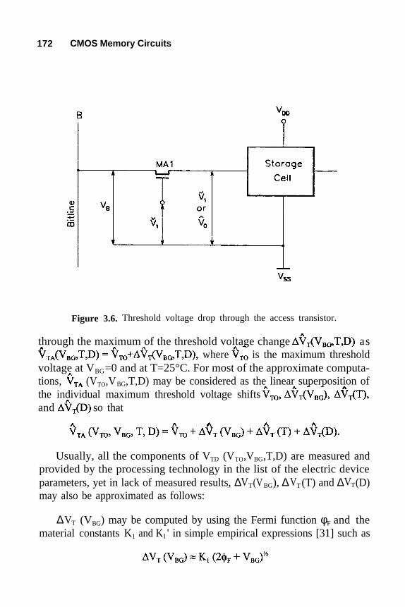
172 CMOS Memory Circuits
Figure 3.6. Threshold voltage drop through the access transistor.
through the maximum of the threshold voltage change aswhere is the maximum threshold
voltage at VBG=0 and at T=25°C. For most of the approximate computa-tions, (VTO,VBG,T,D) may be considered as the linear superposition ofthe individual maximum threshold voltage shiftsand so that
Usually, all the components of VTD (VTO,VBG,T,D) are measured andprovided by the processing technology in the list of the electric deviceparameters, yet in lack of measured results, ∆VT(V BG), ∆VT(T) and ∆VT(D)may also be approximated as follows:
∆VT (V ) may be computed by using the Fermi function φBG F and thematerial constants K1 and K1' in simple empirical expressions [31] such as

Sense Amplifiers 173
for long-channel transistors, and
for short-channel devices.
∆VT (T) for CMOS devices is often approachable by a linear function[32] in the traditional ranges of the operation temperatures as
where KM is a material dependent term, ∆T is a temperature increment andKT is the linear temperature coefficient, e.g., KT = 2.4 mV/°C.
Greatly nonlinear and voltage bias dependent is the variation of VTD asa function of the total absorbed radioactive-radiation dose D [rad(Si)] [33].Radiation induced threshold voltage changes ∆VT(D)s are experimentallyobtained data. These changes are large, and can cause the disappearance ofoperation margins (Section 6.2.2) at a low total dose [rad (Si)]. In additionto radiation total dose effects, transient radiation induced dose rate D[rad(Si)/Sec] imprints may also substantially expand ∆VT(D) (Sections6.1.3 and 6.1.5).
If, in a design VTA (VTO ,VBG,T,D) appears to be prohibitively large,∆VT(V ,T,D) can be eliminated or greatly reduced by increasing VBG 1 onthe gate of an n-channel MA1 or by decreasing Vo on the gate of a p-channel MA1 by ∆V (VT ,T,D).BG
3.1.3.3 Leakage Currents
Leakage currents IL-s reduce both "0" and "1" operation margins, sincethey decrease the signal amplitudes on the bitline by a n ddegrade the levels of data stored in memory cells by Here,is the maximum leakage current, comprises the maximum resistancesof the access transistor and the bitline, is the maximum resistancebetween the data-storage node and the supply or ground node in thememory cell, and and are the maximum -induced voltages whichdegrade the operation margins on the bitline and in the cell, respectively.

174 CMOS Memory Circuits
In the computation of the maximum margin-degradationrepresents the highest leakage current which may appear in the oper-ational, processing and environmental worst cases.
The operational worst-case occurs on the bitline of N memory cellswhen the accessed memory contains a log.1 and all other N-1 memorycells store log.0 (Figure 3.7), or vice versa. When such “all-but-one” datapattern is stored, the cell-current IC, that is generated by the datum of theaccessed memory cell, flows against the accumulated leakage currents ofthe N-1 unselected memory cell IL .
Figure 3.7. A memory-cell current opposes the cumulative leakagecurrent on a bitline.
Inside of a memory cell the degradation of log.0 and log.1 levelsdepends mainly on those leakage currents which percolate through theaccess and the eventual load devices. Cell interim load devices, as in anSRAM cell, compensate the level degrading effects of leakage currents,while the lack of load device, as in a one-transistor-one-capacitor DRAMcell, causes such a significant storage-charge loss by leakage currents thatthe cell’s storage capacitor has to be recharged periodically (Section 2.2.1).

Sense Amplifiers 175
From the various types of leakage currents, which may appear in amemory, the subthreshold current IST , the junction leakage current Ij and,
the eventual radiation-induced leakage current I influence the operationr
margins most significantly. For obtaining the maximum of the cumulativeleakage current
the maximum currents and as well as their environmentaldependency data are usually available in the list of the electricalparameters that is provided by the processing technology prior to thedesign start.
If at the design–start measured data are unavailable the followingapproximation [34] to IST may be applied:
where
I xDS is the maximum specific drain-source current at VGS = VT in the
transistors, W is the transistor channel width, L is the transistor channellength, VGS is the gate-source voltage, VT is the device threshold voltage, kis the Boltzmann constant, T is the temperature in °K, q is the charge of anelectron, α is an adjustment factor, n is the doping concentration, and t isox
the oxide thickness.
Usually Ij is dominated by the Sah-Noyce-Schockley generation-recombination current Igr that results from the presence of defects andimpurities in the semiconductor crystals, and Ij may be approached [35] by

176 CMOS Memory Circuits
where
A is the p-n junction area, w is the depletion width in the p-n junction, τ isthe minority carrier lifetime, ni is the number of electrons residing in theconduction band at maximum operating temperature and Vn is theconsidered volume. In addition to IST and I j the occurrence of other leakagecurrents [36] may also be momentous.
The maximum leakage current IL can mightily be aggrandized byradiation-induced leakage currents Ir -s (Section 6.1). Great Ir -s occur inmemories which operate in radioactive environments (Sections 6.1 and6.3). The effects of radioactive radiations on leakage currents are analyzedand calculated in the literature, e.g., [36], but an actual memory design canonly rely on the experimental data obtainable on that specific CMOSprocessing technology which is to be used for the fabrication of thememory. In some memory designs, the effects of other type of leakagecurrents [37] may also be important.
3.1.3.4 Charge-Couplings
drain and gate-channel capacitances C
and capacitance CW
capacitance CE, bitline resistance RB and capacitance CB, and by the wave-
Charge-couplings vc(t)-s occur mainly through the gate-source or gate-GS, CGD and CGC of the memory cells'
access devices and, eventually, of the bitline decoupling devices (Figure3.8), and alter temporarily the signal levels in the memory cells as well ason the bitline and sense-amplifier inputs. The maximum amount of charge-coupling VC causes either a voltage level increase or a decrease in bothlog.0 and log.1 levels, and modifies both "0" and "1" operation marginsunidirectionally. Magnitude of level- and margin-changes are effected notonly by the capacitances CGS, CGD and CGC, but also by the wordlineresistance R W , sense-enable-line resistance RE and
forms of the wordline and sense-enable control signals.

Sense Amplifiers 177
Figure 3.8. Charge-coupling through parasitic capacitances.
The signal shape, as a function of time in the bitline or on the sense-amplifier inputs vc(t), can conveniently be obtained by computersimulations of the sense circuit. Without the use of a simulation program,an approximate vc(t) function, the maximum charge coupling inducedvoltage shift and, thereby, its influence on the operation margins, maycrudely be estimated by a linear model (Figure 3.9). In this model, ro is theequivalent output resistance of the wordline driver or of the sense-enabledriver circuit, CC is combined of CGS, CGD and CGC and it is the couplingcapacitance between the gate of the access transistor and the data storagenode of the memory cell, or between the gate of the sense-enable deviceand the bitline node, and ro is the resistance between the storage node of

178 CMOS Memory Circuits
the memory cell and the ground VSS or supply voltage VDD or, for thesense-enable device, between the bitline node and the V SS or VDD node.Here, the effects of all other resistances, capacitances and eventual activeelements as well as of all nonlinearities are neglected.
Figure 3.9. Simple charge-coupling model.
A linear analysis of the model circuit, using operator impedances andLaplace transforms, results vc (t) in the bitline or on the sense amplifierinput node as
where 1 is the maximum log.1 level that is allowed to drive the accessdevice. The maximum charge-coupling induced voltage change c thatdegrades the operation margins can easily be obtained by plotting thevc (t) functions or by deriving it from the vc (t) equations. As the expressionfor vc (t) clearly shows, the amount of changes in the operation margins
depends strongly on both time constant τW and τ C in addition to the
amplitude of the driver signal V1 . Usually, the parameters for τ W and τC
are such that the charge coupling induced margin degradations are moresignificant in the access transistors of the memory cells than in the sense-enable devices.

Sense Amplifiers 179
3.1.3.5 Imbalances
Imbalances caused operation margin degradations V I B- S are specific to
those sense circuits which use differential sense amplifiers, and theimbalances reduce both "0" and "1" margins. The phrase imbalanceindicates the nonuniform topological distribution of parameters in thetransistor-devices and in the interconnects which constitute a differentialsense circuit.
Ideally, a differential sense circuit is designed to be electrically andtopologically symmetrical. Symmetrical means, here, that the two halfcircuits of the sense amplifier, the pair of bitlines, bitline loads, memorycells coupled to the bitlines, precharge devices, parasitic and eventualother elements, are mirror images of each other (e.g., Figure 3.10). Despite
Figure 3.10. Differential sense circuit.

180 CMOS Memory Circuits
the most careful efforts to mirror the two half-circuits the effects ofsemiconductor processing, voltage biases, substrate currents, temperaturechanges and radioactive radiations, can cause small and nonuniformvariations in the threshold voltage VT, gain factor β, bitline capacitancesCB , gate-source capacitances CGS, gain-drain capacitances CGD, and in otherparameters. These nonuniform parameter variations manifest themselvesin offsets [38], i.e., in voltage and current differences between the twooutputs of the sense amplifier, when identical precharge voltages appearon its input pair (Section 3.5.1). The sense amplifier offset may act againsteither the log.0 or the log. 1 level. Therefore, imbalances may reduce both"0" and "1" operation margins in a differential sense circuit.
Approximations of the maximum imbalance-caused margin reductionsrequire computer aid, because the effects of the parameter variations aretime-dependent, nonlinear, and interacting. Nevertheless, the qualitativeeffects of variations in a few parameters VT, β, CB and C GS may beillustrated by differentiating the Kirchoff equations, which describe thedifferential sense circuit in matrix form [39], when devices MPL and MPRare used for precharge only and VPR > VDD - VT (Section 3.3.2);
Here, indices L and R designate left and right symmetrical elements of thecircuit, VL and VR are the voltages on the input and output of e senseamplifier, and VS is the common source voltage of transitors ML and MR.From the matrices the estimate of the output signal differential d(VL-VR )/dtmay be summarized in three terms

Sense Amplifiers 181
where K1 and K2 are adjustment factors which are affected by the deviceparameters of ML and MR. In the equation of d(VL -VR )/dt, the first term isthe threshold voltage difference for transistors ML and MR, the secondterm includes the effects of capacitance and gain-factor fluctuations, whilethe third term indicates the dependency on the speed of the sense signaltransient. Larger parameter nonuniformity and feaster transient signalscause larger imbalance, and, by that, larger margin degradations at a givenoperating temperature T. An imbalance-caused margin degradation voltageVIB may be calculated as
where ∆t is the sense amplifier setup time.
In practice, the voltage imbalance VIB may be considered by theanticipated DC offset V of the sense amplifier, so that Voff IB = Voff . Boththe offset voltage and offset current may change slightly with thevariations of temperature and greatly with the amount of radioactiveradiations.
3.1.3.6 Other Specific Effects
A variety of circuit-specific effects may also considerably degrade theoperation margins. For estimation of circuit-specific degradations onemust thoroughly understand the operation of the effected circuit and thecharacteristics of the effect. From the variety of the margin reducingeffects, the following are just a few examples for possible consideration insense circuit designs.
Operation margins may significantly be reduced by the effects of high-amplitude fast-changing electromagnetic noises which may be coupledfrom memory external sources into the sense circuit (Sections 5.2.1 and52.4). Furthermore, in high-density memory circuits the array-internalcrosstalk noises (Section 5.2.2), may also decrease the operation margins

182 CMOS Memory Circuits
substantially. Both "0" and "1" margins may be reduced by the appearanceof either one or both internal and external noise-signals in a sense circuit.
Operation margins in a sense circuit may not merely be decreased, butmay disappear due to the effects of ionizing atomic-particle impacts(Section 5.3) and of various radioactive radiation events on the transmitterand circuit-paramaters (Section 6.1) on the transistor- and circuit-parameters.
Dynamic sense circuits may be plagued by both incomplete bitlinerestore VBR and bitline droop VBD [39]. Both VBR and VBD may counteractthe data signal development on the bitline, and may increase the imbalancein a symmetrical differential sense circuit. Thus, both "0" and "1" oper-ation margins may be reduced by VBR and VBD during sense operation.
3.1.3.7 Precharge Level Variations
Precharge level variations ∆V -s due to the effects of semiconductorPR
processing and environmental variations may reduce both or either one ofthe "0" and "1" operation margins. Both margins are decreased when"midlevel" precharge, and either the "0" or the "1" margin may bedegraded when "low" or "high" level precharge is applied.
A precharge is applied on the bitlines as well as on the inputs and inmany designs, also on the outputs of a differential sense amplifier. Inmany sense circuit designs the precharge voltage serves as a temporaryreference level for the discrimination of log.0 and log. 1 information, and itmay define the initial quiescent operation point for the sense amplifier aswell.
The desirable reference level can be determined by the use of operationmargin diagrams, and can be generated from the supply voltage VDD by aprecharge circuit. A precharge circuit consists of MOS transistors, as wellas passive capacitive and resistive components. The supply voltage,transistor and passive device parameters vary as results of processing,temperature, and radioactive radiation effects, and these variations causedeviations from the desired precharge level. Although precharge levelchanges can be caused by the changes of a wide variety of circuit

Sense Amplifiers 183
parameters, yet the maximum fluctuation of a precharge level ∆ PR isinfluenced predominantly by the percentage variations of the dividerimpedances, or of the threshold voltages of the voltage references (Section4.2.2) (Figure 3.11).
Figure 3.11. Simplified impedance reference circuit (a)and threshold voltage reference circuit (b).
In the divider circuits the precharge voltage V PR fluctuations ∆VPR
maybe expressed as
while in threshold voltage reference circuits the ∆V PR may be approxi-mated by

184 CMOS Memory Circuits
Here, ∆Z1 , ∆Z2 , and ∆VT indicate the total amount of parameter change inimpedances Z1 and Z2 and in threshold voltage V T , and K is an attenuationfactor. K=1 in unattenuated circuits, and K<<1 can be provided by the useof voltage stabilizer circuits.
In precharge generator circuits VPR can track the fluctuations of thesupply voltage VDD and often of other device parameters, e.g., VT, β, CGS,etc. Parameter tracking (Section 6.2.2) implemented in sense circuitsincrease both "0" and "1" operation margins.
3.2 SENSE AMPLIFIERS IN GENERAL
3.2.1 Basics
A sense amplifier is an active circuit that reduces the time of signalpropagation from an accessed memory cell to the logic circuit located atthe periphery of the memory cell array, and converts the arbitrary logiclevels occurring on a bitline to the digital logic levels of the peripheralBoolean circuits (Figure 3.2). The sense amplifier circuit has to operatewithin the conditions that are set by the operation margins (Section 3.1).
The operation margins constrain (1) the minimum and maximum inputsignal amplitudes and , (2) the initial quiescent operation voltageVi (0) = VPR, and (3) the minimum gain for the sense amplifier. The gainA, however, is a function of the initial voltage level or precharge voltageVPR and of the input signal swing (Figure 3.12). Thus, thecombination of VPR and determines basic conditions for senseamplifier designs. In most sense circuits A influences the sense delay t PS,but a high A does not necessarily reduce tPS. Usually, tPS has to becompromised for reduced power consumption and layout area, and forbetter tolerance of environmental effects.
Layout area restrictions for sense amplifiers are specific for memorydesigns. In memories sense amplifier layouts should fit either in the bitlinepitch when each bitline requires individual data sensing as in DRAMs, orin the decoder pitch when a multiplicity of bitlines are connected to asingle sense amplifier as in SRAMs and ROMs. The bitline pitch is

Sense Amplifiers 185
determined by the size of a memory cell, and the decoder pitch is limitedby the number of parallel running decoder wires in the layout design.
Figure 3.12. Sense amplifier gain as a function of precharge voltageand input-signal swing.
The circuit design of a sense amplifier need not to aim linearity inamplification; in fact, sense amplifiers operate in both linear (small) andnonlinear (large) signal-gain domains of their IDS (VDS, VGS) andVo (Vi ) characteristics (Figure 3.13). Here, IDS is the drain-source current,VDS , VGS, Vo and Vi are the drain-source, gate-drain, output and inputvoltages in the sense amplifier. Linear amplification appears in the vicinityof the assumed quiescent operation point Q where both n- and p-channelMOS transistors operate in their saturation regions, and where thesaturation characteristics of MOS devices are nearly linear. Signals outsideof the linear region of the transfer characteristics result in distortednonlinear amplification. This dual, linear and nonlinear, property of MOSsense amplifiers indicates the application of DC, AC and transientanalyses in designs, and the mixed nature of sense amplifier
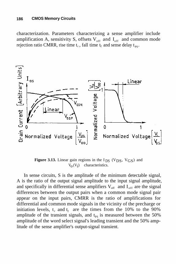
186 CMOS Memory Circuits
characterization. Parameters characterizing a sense amplifier includeamplification A, sensitivity S, offsets Voff and Ioff and common moderejection ratio CMRR, rise time tr , fall time tf and sense delay tPS.
Figure 3.13. Linear gain regions in the I DS (VDS, VGS) andVo (Vi) characteristics.
In sense circuits, S is the amplitude of the minimum detectable signal,A is the ratio of the output signal amplitude to the input signal amplitude,and specifically in differential sense amplifiers Voff and I off are the signaldifferences between the output pairs when a common mode signal pairappear on the input pairs, CMRR is the ratio of amplifications fordifferential and common mode signals in the vicinity of the precharge orinitiation levels, t r and tf are the times from the 10% to the 90%amplitude of the transient signals, and tPS is measured between the 50%amplitude of the word select signal's leading transient and the 50% amp-litude of the sense amplifier's output-signal transient.

Sense Amplifiers 187
3.2.2 Designing Sense Amplifiers
Sense amplifier design objectives combining
•
•
•
•
•
specified environmental tolerance
minimum sense delay,
required amplification,
minimum power consumption,
restricted layout area,
high reliability,
•
are difficult to meet due to the contradictory effects of circuit complexityand transistor sizes on the individual design goals.
To optimize the combination of design goals the circuit designer maymanipulate only the circuit configuration, and the sizes and shapes of thecircuit-constituent transistors, capacitors, resistors and interconnects. Theother transistor and passive-element parameters and their variations aredetermined by the effects of the processing technology, power supply,temperature and radioactive radiations. Because the design parametershave to satisfy a number of contradictory requirements, and because lessnumber of equations than the number of unknowns are at the designer'sdisposal, the sense circuit design is a highly iterative procedure.
Sense amplifier design procedures aim to reduce the number ofiterations by partitioning the design into four major phases: (1) prelim-inary design, (2) circuit analysis, (3) reliability and environmentaltolerance analysis, and (4) final design (Table 3.1).
The Preliminary Design phase makes possible to adopt or devise abasic sense amplifier circuit that most likely satisfies the design goals.Investigations on experimental designs of candidate sense-circuitarchitectures and schematics provide operation margins and prechargelevels, as well as speed, gain and layout data, which are approximate.These approximations are, however, sufficient to select a basic sense

188 CMOS Memory Circuits
amplifier circuit that performs acceptably within the limitations dictatedby the processing technology and environmental effects.
The results of the Circuit Analysis assists to approximate the finalcircuit diagram, MOS transistor sizes, operation, timing and layout of thebasic sense amplifier. Initially, a direct current (DC) analysis of the sense
1. Preliminary Design
Sense Circuit Architecture and Schematic
Operation Margin and Precharge Analysis
Sense Amplifier Circuit
2. Circuit Analysis
Direct Current
Small Signal Alternative Current
Large Signal Transient
Timing
Layout
3. Reliability and Environmental Analysis
Operation Stability
Hot Carrier Suppression
Temperature Effects
Atomic Particle Impact
Radiation Hardness
4. Final Design
Layout Integration
Timing Integration
Complete Analysis
Table 3.1. Design phases.

Sense Amplifiers 189
amplifier circuit establishes the quiescent operation point and voltagebiases and, furthermore, the crude aspect ratios of the MOS transistors.Next, the aspect ratios, and the circuit itself, may be modified to providethe desirable alternative current (AC) characteristics, such as gain as afunction of the precharge voltage and input voltage swing, common moderejection ratio, offset, etc. Following the AC analysis an examination oflarge signal transient or time (t) behavior reveals the switching signalforms as functions of time. To approach the objectives in switching timesand delays, usually further changes in MOS device sizes and capacitorsand the inclusion of additional circuit elements are needed. The operationof the circuit elements cause ripples, spikes, delays, and other anomalies inthe sense operation. Often, these anomalies can be minimized by propertiming of the part circuits. Moreover, the timing is of fundamentalimportance to provide the conditions that are assumed for the analyses.Furthermore, the analysis must consider the layout limitations, andinvestigate whether the circuit can be placed into the available place andhow the physical implementation of the circuit effects the operation of thememory circuits.
Reliability and Environmental Analysis may effect the memorycircuits considerably, but usually it does not impose substantial changes inthe basic sense amplifier circuit. The sense amplifier circuit may needadditional circuit elements, and sometimes complete circuits, to providestable operation throughout the specified temperature range, to avoid hotcarrier emission induced reliability degradations, to reduce soft-error-ratesresulting from impacts of alpha or of a variety of cosmic particles in space,and to harden against eventual ionizing radiations in nuclear environ-ments.
A Final Design integrates the layout and timing of the memory cellarray, decoders, write and read circuits with the layout and timing of thesense circuit. The unification of layout and timing may effect the senseamplifier operation and design. To finalize the design a completereanalysis that includes all changes and effects has to be performed.
The analysis of the sense amplifier circuit heavily relies on computeraid, and requires the use of the most sophisticated MOS device models incircuit analysis programs. Particularly, the MOS device model for a

190 CMOS Memory Circuits
submicrometer sense circuit simulation should comprise velocitysaturation, substrate currents, subthreshold characteristics, drain inducedbarrier lowering, drain-source capacitance, threshold voltage dependencyfrom channel length and width in addition to the parameters of thetraditional MOS device models.
3.2.3 Classification
Sense amplifiers may be classified by circuit types such as differentialand nondifferential, and by operation modes such as voltage, current andcharge sense amplifiers (Table 3.2)
Sense Amplifiers
Circuit Types Operation Mode
Differential Voltage
Nondifferential Current
Charge
Table 3.2. Sense amplifier classification.
Differential sense amplifiers are applied in the vast majority of CMOSmemories including all SRAM, DRAM, many ROM, and other memorydesigns. In such designs the sense amplifiers are coupled to a pair ofidentical bitlines. Nevertheless, the bitline pairs do not necessarily carry apair of complementary signals (log.0 and log.1), but on one of the bitlinesa reference level may be provided, while the other one supplies the datasignal. The minimum signal amplitudes, which are distinguishable fromnoises on bitline pairs, are significantly smaller than those on singlebitlines. Since a differential sense amplifier can distinguish smaller signalsfrom noise than its nondifferential counterpart, the signal detection canstart sooner than that in a nondifferential sense amplifier. Although differ-ential sensing compromises some silicon area, yet in most of the designs

Sense Amplifiers 191
the use of differential amplifiers allow to combine very high packingdensity with reasonable access time and low power consumption.
Nondifferential sense amplifiers find application in those nonvolatileand sequential memories, where the memory cells are capable to generatesignificantly larger and faster signals on a bitline than DRAM and SRAMmemory cells do. Nonetheless, the evolution of the nonvolatile andsequential memory technology toward higher density and performanceplaces stringent requirements on sense amplifiers which can hardly besatisfied by nondifferential approaches.
In conventional memories both differential and nondifferential senseamplifiers operate in voltage amplification mode, because the very largeinput resistance of the MOS transistors allow for obtaining high voltagegain and voltage swings by application of simple circuits. However, thespeed of sense circuits, which sense voltage differences, is limited by thecharge and discharge times of the circuit-inherent capacitive elements.
In advanced memories the speed limitation resulting from high bitlinecapacitances, may be encountered by the application of current-modesense amplifiers. Current-mode sense amplifiers can greatly reduce thecharge and discharge times of the capacitances by their low input andoutput resistances. Furthermore, current-mode sense amplifier designs canprovide speed-power products, which are superior to other approaches.
Some memories, as an alternative approach to improve sensing speed,apply charge-transfer or other type of preamplifiers placed before avoltage-mode sense amplifier. Nonetheless, the performance of the pre-amplifier-plus-voltage amplifier compound is inferior to that of purelycurrent-mode sense amplifiers, in most cases.
This chapter, therefore, focuses on differential voltage-mode anddifferential current-mode sense amplifiers, and discusses nondifferentialand charge transfer sense amplifiers in accordance with their decliningimportance in memory designs.

192 CMOS Memory Circuits
3.3 DIFFERENTIAL VOLTAGE SENSE AMPLIFIERS
3.3.1 Basic Differential Voltage Amplifier
3.3.1.1 Description and Operation
Differential amplifiers have been known for a long time [310], and thedifferential sense amplifiers have been derived from the basic MOSdifferential voltage amplifier (Figure 3.14). Importantly, this basic circuitcontains all elements required for differential sensing, easy to analyze, andthe results, principles and tradeoffs are readily applicable in the design ofall other differential voltage sense amplifier circuits. Moreover, the designtradeoffs in this basic circuit demonstrate the necessity and justify the useof more complex sense amplifier circuits.
Figure 3.14. Basic differential voltage amplifier circuit.
The basic voltage differential amplifier consists of two enhancement-mode MOS devices M1 and M2 and three resistive elements RL1 , RL2 andR . Transistors M1 and M2 are assumed to be identical and to operate inS
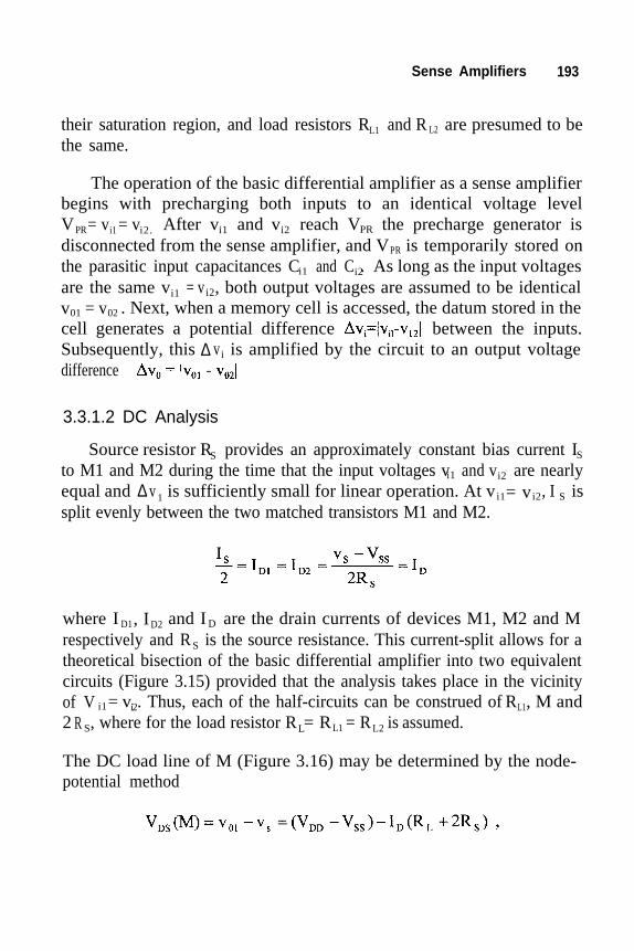
Sense Amplifiers 193
their saturation region, and load resistors RL1 and R L2 are presumed to bethe same.
The operation of the basic differential amplifier as a sense amplifierbegins with precharging both inputs to an identical voltage levelVPR= vi1 = vi2. After vi1 and vi2 reach VPR the precharge generator isdisconnected from the sense amplifier, and VPR is temporarily stored onthe parasitic input capacitances Ci1 andare the same vi1 = v i2, both output voltages are assumed to be identicalv01 = v02 . Next, when a memory cell is accessed, the datum stored in thecell generates a potential differenceSubsequently, this ∆ vi is amplified by the circuit to an output voltagedifference
Ci2. As long as the input voltages
between the inputs.
3.3.1.2 DC Analysis
Source resistor RS provides an approximately constant bias current IS
to M1 and M2 during the time that the input voltages vi1 and vi2 are nearlyequal and ∆ v 1 is sufficiently small for linear operation. At vi1 = vi2, I S issplit evenly between the two matched transistors M1 and M2.
The DC load line of M (Figure 3.16) may be determined by the node-potential method
where I D1, ID2 and I D are the drain currents of devices M1, M2 and Mrespectively and R S is the source resistance. This current-split allows for atheoretical bisection of the basic differential amplifier into two equivalentcircuits (Figure 3.15) provided that the analysis takes place in the vicinityof V i1 = vi2. Thus, each of the half-circuits can be construed of RL1, M and2 R S, where for the load resistor RL = RL1 = RL2 is assumed.

194 CMOS Memory Circuits
Figure 3.15. Bisected basic differential amplifier circuit.
Figure 3.16. Determination of the DC load line.

Sense Amplifiers 195
where v01 is the output voltage and vs is the source potential of transistorM. Since in most of the memories Vs s = 0, then the two extreme points ofthe DC load line in the characteristic field of M1 or M2 may bedetermined as ÎD = VDD/(RD+2R S) at VDS=0 and DS =V DDat I D=0. By meansof the DC load line and the gate voltage of transistor M, e.g., VGM= vi l- vs,for any quiescent operation point X; the drain current IDX and voltage VDX
and, in turn, the channel width W and channel length L of transistor M andthe resistances RL and RS , can be approximated. Namely, the saturationcurrent of a submicrometer MOS transistor IDSAT may roughly be estimated[311] by
where εox is the specific permittivity of the gate oxide, t ox is the thicknessof the gate oxide, v∞ is the saturation velocity of the electrons or holes, VPR
is the precharge voltage, VT is the threshold voltage, and VBS is thesubstrate bias of device M. This estimation is rough because the aboveequation for I DSAT treats the carrier transport problem within the channelinaccurately, and disregards the two-dimensional current flow. Fordescription of the saturation current IDSAT of a long channel MOS devicethe traditional first-order approach [312] may be used;
where µ is the mobility and µ = f(VPR - v s).
Since the same amount of current flows through MOS device M andresistors RL and 2RS current ID can be expressed as
In the introduced equations, L, C ox v∞ and µ are MOS device parameterswhich are determined by the processing technology, the supply voltageVDD is available from the design specification, precharge, source and

196 CMOS Memory Circuits
Applying Kirchoff's current-loop law for the Thevenin equivalentcircuit, the differential-mode gain Ad, the common-mode gain Ac, and thedifferential output voltage ∆ vo may be expressed as
output voltages VPR, Vs and vo are predetermined by the internal operationand noise margins of the sense circuit and of the circuit driven by the senseamplifier. With these device and circuit parameters, W or W/L as well asRL and R S can be obtained from the above equations to any practical ID .
The drain current ID can well be approximated, because it has upperand lower boundaries IDU and IDL. IDU is constrained by the allowablesubstrate current to avoid hot-carrier emission caused reliability problems,by the available layout area to fit into a cell or decoder size dictated pitch,and by the maximum permissible power dissipation of the memorypredetermined as one of the design goals. I DL is restrained by theamplification required to provide adequate signal amplitudes for the inputsof the peripheral logic circuits, by the CMRR sufficient to suppresscommon mode signals below the permissible noise level, and by themaximum propagation delay allowed for the sensing. With the maximumand minimum permissible drain currents Î D and D the gain factor β as wellas the channel width W and length L for the transistor M can beapproached.
3.3.1.3 AC Analysis
The small-signal, low-frequency Norton and Thevenin equivalents(Figure 3.17) of the basic differential voltage amplifier circuit (Figure3.44) can be used to estimate the differential gain Ad, common mode gainA c and common mode rejection ratio CMRR [313].

Sense Amplifiers 197
Figure 3.17. Norton and Thevenin equivalents of thebasic differential amplifier circuit.

198 CMOS Memory Circuits
Here, gm is the transconductance and rd is the dynamic drain-sourceresistance for driver devices M1 and M2, RL is the load resistance, and RS
is the common source resistance. If rd>>RL, then the differential andcommon mode gains Ad and Ac are
and the common mode rejection ratio, CMRR is
Parameters gm and rd may most conveniently be varied by the channel-width W and the channel-length L of the identical driver devices M1 adM2. The aspect ratio W/L of M1 and M2 and resistances RL and RS shouldbe designed so that the position of the precharge voltage VPR approximatesthe center of the high-gain linear portion of the input-output transfer curvevo=f (vi) (Figure 3.18) to assure high initial amplification Ad . To match the
Figure 3.18. Precharge voltage position for high initial gain.

Sense Amplifiers 199
high-gain linear portion of the transfer curve with the predetermined VPR
by varying W, L, RD and RS is an untrivial task, because Ad is a functionalso of the gate-source voltage VGS of transistors M1 and M2 and therebyof VPR through the carrier mobility µ(VGS,…), gm(VGS,…), andrd(µ,VGS,…) besides the dependence of Ad from other parameters.
In practice, increased gm is obtained by increased device aspect ratioW/L and by lowered VT, and larger rd is acquired by decreased bias voltageV PR-VS on transistors M1 and M2. Moreover, for M1 and M2 some senseamplifier designs use depletion devices to improve gm and rds.
Because gm/area of n-channel MOS devices has been larger than that ofp-channel devices, traditional designs apply NMOS enhancement devicesfor M1 and M2. However, when Leff < 0.15 µm, p-channel devices mayprovide about the same gm/area as n-channel devices do due to the effectsof the carrier velocity saturation. Since p-channel devices have somewhatlarger rd than their n-channel counterparts do on the same layout area, p-channel devices may also be used for M1 and M2.
Improvements in gm and rd of transistors M1 and M2 alone, nonethe-less, would result in little increase in Ad and CMRR if resistances RD andRS are small. A direct application of large RD and RS in the basicdifferential voltage differential amplifier, however, would result inunacceptable slow output signal changes when the outputs drive the ratherlarge capacitive loads CL1 and CL2. Moreover, the imperfect symmetricalnature of M1-M2, RL1 -RL2 and CL1-CL2 pairs result in high offset voltages,which limits the detectable signal amplitudes and delays the start of thesense operation.
Because of the rather slow operational speed provided at considerablepower dissipation and because of the inherently high offsets, the basicdifferential voltage amplifier is not applied in memories in the discussedprimitive form. Nevertheless, the DC and AC analyses of the basicdifferential voltage amplifier have fundamental importance in designingother type of sense amplifiers.

200 CMOS Memory Circuits
3.3.2 Simple Differential Voltage Sense Amplifier
3.3.2.1 All-Transistor Sense Amplifier Circuit
The simple differential sense amplifier (Figure 3.19) applies transistorsMN1 and MN2 as driver and MN3 as source devices, transistors MP4 andMP5 as open-circuits, i.e. very high resistance loads at small signalamplification, and as medium-resistance load-transistors at large signalswitching. At the start of the amplification the open-circuit load allows for
Figure 3.19. Simple differential voltage sense amplifier circuit.
high initial amplification Ad and low offset voltage Voff. Ad becomes largerwith increasing load-resistances, and Voff gets smaller because the effectsof nonsymmetricity in the load-device pair MP4-MP5 are eliminated.Furthermore, source transistor MN3 acts as a nearly constant currentsource and, thus, increases CMRR during small-signal operation. Whenthe output-signal swing is large enough, i.e., it can be discriminated fromthe noises, then requirements for great Ad, large CMRR and small Voff

Sense Amplifiers 201
become unimportant, and load-transistors MP4 and MP5 can be turned on.The activated MP4 and MP5 provide fast large-signal pull-ups throughtheir rather small drain-source resistance. The drain-source resistance ofMN3 may also be increased by temporary gate voltage increase. In thisdifferential voltage sense amplifier devices MN1, MN2, MN3, MP4 andMP5 have the same respective functions as elements M1, M2, RS, RL1 andRL2 in the basic differential amplifier (Section 3.3.1) do.
The operation of the voltage sense amplifier commences at a turned-off MN3 and turned-on MP4 and MP5. Devices MP4 and MP5 prechargethe outputs to VPo = v01 = v02, and other devices (not shown) precharge theinputs to VPi = vi1 = vi2 . An identical precharge voltage VPR = VPo = VPi forboth the inputs and outputs are applied in many sense circuits forreductions of transistor counts. After the precharge, VPR is temporarilystored on the input capacitances, and both devices MP4 and MP5 areturned off. Next, source device MN3 is turned on slightly, and a memorycell connected to the bitlines is accessed. The accessed memory cellgenerates a small voltage difference ∆vi between the two input nodes, and∆ vi is amplified to an output signal ∆vo = Ad ∆ vi which appear between thetwo output nodes, while any common mode signal change is reduced bythe factor of CMRR. Ad and CMRR reduce gradually as ∆vo exceeds thelinear region of the sense amplifier operation and when ∆larger than the noise levels, load devices MP4 and MP5 and source deviceMN3 are turned on again to enlarge output currents.
vo becomes
3.3.2.2 AC Analysis
During the linear amplification the load resistances are very large andsource current IS is approximately constant, because transistors MP4 andMP5 are turned off and MN3 operates in its current saturation region(Figure 3.20). The nearly constant current and the large resistive loadspromote high Ad and high CMRR.
When load transistors MP4 and MP5 are turned off, their drain-sourceresistances rd4 = rd5 = rdL are determined by the output leakage currents IoL4
and I oL5 as

202 CMOS Memory Circuits
while the initial drain-source resistance rd3 of MN3 may be viewed as theoutput impedance of a current source [314].
Figure 3.20. Rudimentary model for small signal amplification.
Here, λ is an empirical saturation coefficient and IS is the drain-sourcecurrent of device MN3. If the drain-source resistances rd1 and rd2 of thedriver transistors MN1 and MN2 and the resistance rd3 are much smallerthan rdL , then both Ad and CMRR are large. However, neither high Ad norhigh CMRR are needed after the amplitude of ∆vo clearly exceeds thenoise levels, e.g., vo = 0.1VDD, but then speedy pull-ups and pull-downs ofthe individual output voltages vo1 and vo2 toward the potentials VDD or V SS,are required. The large-signal transients of ∆vo are fast even when the

Sense Amplifiers 203
amplifier drives large capacitive loads, if the output currents are large.Increases in the output currents i1 and i2 are obtainable through decreasedoutput resistances, which decrease may be provided by turning devicesMN3, MP4 and MP5 on hard and, thereby, greatly reducing their drain-source resistances rd3, rd4 and rd5.
3.3.2.3 Transient Analysis
The transient analysis should include the nonlinearities in thecharacteristics of all constituent devices MN1, MN2, MN3, MP4 and MP5as well as of the equivalent load capacitance CL, which makes thecomputations of signal rise, fall and propagation delays rather difficult.Therefore, computer programs with high-level complex device models areroutinely used in sense amplifier designs. Nonetheless, to reduce designtimes and to understand the effects of individual parameters on thetransient characteristics crude approximations, which disregardnonlinearities, may beneficially be applied.
L
The linear equivalents of the bisected basic CMOS sense amplifier thatcharges and discharges a linear capacitive load C (Figure 3.21) allow toemploy Laplace-transform, and to obtain the operator impedance Z(p) ofthe circuit
where rdD and 2rdS are the drain-source resistances of devices MD and MSrespectively.
The Laplace-transformed of the discharge current If(p) of CL, when CL isprecharged to a midlevel VPR that provides approximately the same extentsfor both "0" and "1" operation margins, is

204 CMOS Memory Circuits
Figure 3.21. Bisected simple CMOS sense amplifierand its linear equivalent circuits.
The reverse Laplace transformation of If (p) into the time domain givesthe time function of the fall-current if (t), and if (t)(rdD + 2rdS) results thetime function of the fall voltage vf(t);
Similarly, the time function of the rise current ir(t) and voltagevr(t) during the charge of CL may be obtained by using time contstant
τ r = CLrdL, where rdL is the drain-source resistance of ML. Assumptions,here, include that all elements rdD , rdS, rdL and CL can be characterized bylinear concentrated parameters, the effects of parasitic elements on thetransient signals are negligible, and the current through ML is very little incomparison to the total discharge and charge currents.

Sense Amplifiers 205
Both the discharge and charge are clearly nonlinear operations,because rdD, rdS , rdL and CL are functions of if (t), vf (t), ir(t) and vr(t). Yet,each of the output signals vf (t) and vr(t) (Figure 3.22) may be approx-imated by using piecewise linear functions in MD's VDS = f(ID, V GS) char-
Figure 3.22. Output signal of the simple CMOS sense amplifier.
acteristics for two separate time intervals t2-t 1 and t3-t2. Here, t2 -t1 is thetime interval during MD operates in the saturation region, and t3 -t2 is thetime interval MD operates in the triode region. Drain-source resistances rd -s in both saturation and triode regions may be approached by linearfunctions, if it can be assumed that during t2-t 1 the gate voltages VPR± ∆vi /2and Vs of devices MD and MS, and during t3 -t 2 the gate voltage V L o fdevice ML, change very little. Applying the equations of vf (t) and vr(t) tointervals t2-t1 and t3-t 2 and using the piecewise linear approximation to rdD ,

206 CMOS Memory Circuits
rdS and rdL; the fall-time tf and the rise time tr of the output signal can beestimated as
In these equations, designations SAT and TRI indicate MOS deviceoperations in the saturation and triode regions of MOS devices, respec-tively, and VDSAT is the drain-source voltage at which the carrier velocitysaturates. VDSAT is not only a function of the critical electrical field strengthat which the carrier velocity saturates EC, but also of the effective channellength of the MOS device Leff and the voltages VGS, VT and VBG [315] as
where VGS is the gate-source voltage of the MOS device.
To shorten the duration of signal-transients, resistances rdD, rdS , rdL andthe voltage VDSAT can be manipulated in the design by varying theeffective channel width Weff and length Leff , and by adjusting the gate-source voltage VGS in each individual MOS device MD, MS and ML, butonly within the boundaries imposed by the DC and AC conditions ofoperation. For large Ad and CMRR the AC analysis suggests large rdD, r dS
and rdL, but the expressions of transient times tf and t r indicate that all r dD ,rdS and r dL should be small for short sensing time. This tradeoff, Ad andCMRR versus tf and t r, is alleviated in most practical designs by thepreviously described switching from initial large rdL and rdS to small rdL and
Sense Amplifiers 207
rdS by changing the gate voltages of transistors ML and MS at a certainsmall output signal amplitude.
Reductions in t f and t r, by increasing Weff in devices MD, ML and MS,are limited by restrictions in layout area, power dissipation, substratecurrent and input capacitance of the sense amplifier, while the minimumLeff is determined by the processing technology. The magnitude of theoutput-load capacitance CL of the sense amplifier depends mainly on thearchitecture of the memory array through parasitic capacitances of longinterconnects and by the input capacitances of the circuits driven by thesense amplifier. By placing a buffer amplifier in the immediate vicinity ofthe sense amplifier output the capacitance CL can greatly be reduced.
Apart from decreasing rdL , r dS, r dD and CL a widely applied method toreduce tf and tr is the limitation of the output signal swing ∆vo to an smalloptimized voltage (Section 3.3.6.5).
In both full-swing and optimized-amplitude operation modes only oneof both appearing output signals, the rising one, can be accelerated by thesimultaneous switching of both load devices MP4 and MP5 from high tolow drain-source resistances. This simultaneous switching of load devicesis a fundamental drawback of the simple differential voltage senseamplifier in obtaining fast sensing operation.
3.3.3 Full-Complementary Differential Voltage Sense Amplifier
3.3.3.1 Active Load Application
The full-complementary sense amplifier (Figure 3.23) reduces theduration of the signal-transients by using active loads in large-signalswitching, and improves the small-signal amplification Ad and commonmode rejection ratio CMRR by providing virtually infinite load resistancesand approximately constant source current of the inception of signalsensing. In these sense amplifier the active load is implemented intransistors MP4 and MP5, and transistors MN3 and MP6 serve asswitchable source devices. When devices MN3, MP6 and MN7 areactivated transistor triad MP4-MP5-MP6 operates with triad MN1-MN2-

208 CMOS Memory Circuits
MN3 in synergy, and together they form a high-speed complementarypush-pull amplifier.
Figure 3.23. Full-complementary differential voltage sense amplifier.
The operation of the active-load full-complementary differentialvoltage sense amplifier is similar to that of the previously described simpledifferential voltage sense amplifier. Prior to the sense amplifier activationsource transistors MN3, and MP6 and MN7 are turned off, and all inputand output nodes are precharged, through devices which are not shownhere, to vi1 = vi2 = v01 = v02 = VPR. First, device MN3 is turned on, thisactivates the differential amplifier combined of devices MN1, MN2, MN3and of open-circuit-loads, and the circuits amplifies to
When ∆vo is large enough to approach the cutoff voltage ofeither MN1 or MN2, source device MP6 is turned on and MP6 connectsload devices MP4 and MP5 to VDD. When either one MP4 or MP5 gets cutoff, the other one pulls the positive-going signal toward the supply voltagerapidly through the decreasing drain-source resistance of MP4 or MP5.Similarly, low resistance path occurs also for the negative-going signal

Sense Amplifiers 209
through device MN1 or MN2. The activation of high-current device MN7shunts source transistors MN3 and further accelerates the output-signaldevelopment. For fast signal pull-ups the drain-source current of deviceMP6 is also high.
3.3.3.2 Analysis and Design Considerations
All methods and results of DC, AC and transient analyses usedpreviously in the examination of the basic and simple differential voltagesense amplifiers (Sections 3.3.1 and 3.3.2), can also be applied to theanalysis and design of the full-complementary differential sense amplifier.The operation of the full-complementary sense amplifier may be dividedinto three segments (1) small signal amplification, (2) signal pull-downand (3) signal pull-up, and the circuits made up by the devicesparticipating in these three operational segments (Figure 3.24) demonstratethe affinity between the full-complementary and the basic and simpledifferential sense amplifiers.
Figure 3.24. Devices participating in small-signal amplification,large signal pull-down and pull-up.
The full-complementary differential sense amplifiers' speed-powerproduct can be enhanced by designing its operation so that at an optimum

210 CMOS Memory Circuits
output voltage swing (Section 3.3.6.5) ∆vopt = ∆vo<<VDD-VSS
one of bothdevices MN1 or MN2 and simultaneously one of both devices MP5 orMP4 cut off in a complementary-differential fashion. This selective cut offinterrupts the direct current flow between VDD and VSS, decreases thesignal transient times and the power dissipation. Moreover, a signalamplitude limitation by turning off devices MN3, MP6 and MP7 at ∆vopt
reduces the propagation delay and power of the signal transmissionbetween the sense amplifier and the read circuits.
The operational speed of the full-complementary differential amplifiercircuit is often hiked also by implementing transistors MN1, MN2, MP4and MP5 as zero-threshold-voltage devices in separate p- and n- wells[316] (Figure 3.25). A threshold voltage that is set to zero increases theeffective gate voltage VGeff = VGS - VT (VBG) of the MOS device, and thehigher VGeff results in higher drain-source current and faster signaldetection. The well separation allows for minimizing the VT(VBG)fluctuation by controlling VBG through VBP and VBN, and the reducedVT(VBG) fluctuation decreases the offset and the time to develop a validoutput signal, in addition to the improvement in the signal detectionsensitivity.
Figure 3.25. Reduction of back-gate bias effects by well separation.

Sense Amplifiers 211
The full-complementary differential sense amplifier is able to combinehigh initial gain, common mode rejection ratio and fast operation, and hasa large input and a small output impedance. The operation can be madeeven faster by using positive feedback (Sections 3.3.4 and 3.3.5) whichprovides an enhanced initial differential amplification and an instant datarewrite into the memory cells at destructive read-out.
3.3.4 Positive Feedback Differential Voltage Sense Amplifier
3.3.4.1 Circuit Operation
The positive feedback in differential sense amplifiers (1) makes poss-ible to restore data in DRAM cells simply, (2) increases differential gain inthe amplifier, and (3) reduces switching times and delays in the sensecircuit.
The positive feedback differential amplifier (Figure 3.26) has two data-terminals and , and each of both terminals acts as a common input and
Figure 3.26. Positive feedback differential voltage sense amplifier circuit.

212 CMOS Memory Circuits
output for the circuit [317]. In the circuit, a simple crosscoupling betweenthe drains and gates of devices MN1 and MN2 implements the positivefeedback.
Before the start of the positive-feedback sense operation, the accessedmemory cell generates a small voltage difference vi(0)-v2(0) on the bitlinesand on the sense amplifier nodes and , and the source device MN3 andload devices MP4 and MP5 are turned off and feedback devices are biasedto operate in the saturation region. The positive feedback operation, and thesense signal development (Figure 3.27) start, when clock φs turns MN3 on,and input/output nodes and are decoupled from the bitlines (Section
Figure 3.27. Input/output, common mode and source signals.
3.3.6.2.) at the time t=to. After t=to both potentials v1(t) and v2(t) of nodesand fall simultaneously toward Vss through the dynamic drain-source
resistances rd1, rd2 and rd3 of devices MN1, MN2 and MN3 and, con-

Sense Amplifiers 213
currently, potential difference v1(t)-v2(t) increases. As v1(t) and v2(t) falland v1(t)-v 2(t) grows simultaneously, one of both devices MN1 or MN2,e.g., MN1, is cut off and the other device, e.g., MN2 begins to operate inthe triode region at the time t=tSAT. About at t=tSAT, clock φL turns loaddevices MP4 and MP5 on, and the rising signal, e.g., v1(t), is pulledtoward VDD rapidly. The pull-down of the descending signal, e.g., v2(t), isalso quick, because MN2 receives high gate voltage from the rising v1(t),and because MN3 can be turned on hard or shunted by an additional highcurrent device (Section 3.3.3.1).
3.3.4.2 Feedback Analysis
Positive feedback effects can exist exclusively in the operating regionwhere the complex loop gain A1A2 satisfies the Barkhausen criteria
Here, without the numerical subscripts, is the complex ampli-fication, A is the low-frequency small-signal gain, and ρ is the phase anglefor one half of the bisected symmetrical differential sense amplifier. Inmirror-symmetrical feedback amplifiers the Barkhausen criteria definestwo requirements
where n = 0, 1, 2, ... and 0. Both requirements should befulfilled for a possible wide range of v1(t) and v2(t) rather than in a smallvicinity of VPR to benefit from the effects of positive feedback. Thedifferential gain A'd of a differential positive feedback sense amplifier(Section 3.3.1.3), that is mirror symmetrical, can be expressed as
where Ad is the differential amplification without feedback, gm and rd arethe transconductance and the drain-source resistance of the driver tran-sistors MN1 and MN2.

214 CMOS Memory Circuits
Transient analysis of positive feedback amplifiers, even in rudimentaryapproaches are cumbersome, because of the interdependency of the para-meters which determine the sense signal v1(t) and v2(t). To simplify theanalysis of the large signal model (Figure 3.28), however, two importantobservations can be used: (1) the time function of the common modevoltage vC(t) = [v1(t)+v2(t)]/2 follows the source signal vS(t) closely untilthe time either one of the devices MN1 or MN2 enter into its saturationregion tSAT and somewhat loosely between tSAT and the time either MN1or MN2 cuts off tcut and (2) during most of the switching time untilt = tSAT both MN1 and MN2 operate in their saturation region [318].Thus, until the time when MN1 or MN2 cuts off, the voltage differencevC(t) - vS(t) = v GS(0) = V PR - vS(0) ≈ Constant, where vGS(0) and vS(0) arethe initial gate-source and source potentials of MN1 and MN2 just beforet = to.
Figure 3.28. Large signal model.

Sense Amplifiers 215
If the sense amplifier starts to operate at t = to, and the load devicesMP4 and MP5 are turned on at t = t SAT, then the time of the differentialsignal development td can be approached as a sum of two terms
where tCS is the time when the signal v1(t) or v2(t) reaches the amplitude of0.1 VDD or 0.9 V DD, whichever appears earlier.
Term (tSAT -to) may first be approached by assuming that the sourcevoltage vS (t) = vS(0) = Constant, and by modeling the crosscoupled circuitof MN1 and MN2 as a primitive flip-flop or static memory cell (Sections2.4 and 2.5) in which the load devices are of extremely high resistances.When a perfectly symmetrical flip-flop brought to its equilibrium voltagevC = v1(0) = v2(0) = vGS(0), an infinitely small initial voltage jump ∆Vo1(t)causes exponential changes on both node voltages v 1(t) and v2 (t);
where vGS is the drain-source voltage of the driver device MN1 or MN2,
and τ is a constant, as it is known from the feedback theory. In thispositive feedback voltage sense amplifier, however, the source voltagevs(t) changes with time, and vS(t)=vS (0) is valid only at t o. For an arbitraryvS(t), with vC(t) - vS(t) = VPR - vS(0), may be written
where VT is the threshold voltage, and VBG is the substrate bias. A sub-traction of v2 (t) from v1(t), at the assumption of constant and identical athreshold voltage V T for the transistors MN1 and MN2, results thedifferential voltage change vd(t) from to to tSAT

216 CMOS Memory Circuits
and the time until either MN1 or MN2 enters to its triode region
At the assumptions that devices MN1, MN2, MP4 and MP5 are ofidentical sizes, and both devices MN1 and MN2 operate in the saturation
region, the time constant τ SAT may be approximated by
where CB is the bitline capacitance, CGS and CGD are the gate-source andgate-drain capacitances for devices MN1, MN2, MP4 and MP5 and β isthe gain factor for devices MN1 and MN2. By applying this τSAT andsetting vd(tSAT) = VT(VB) the duration of tSAT-to can be estimated.
In the estimation of the time-period tC S-tSAT , the presumption that tC S i sthe time point t0.9 when the rising output signal v1(t) achieves0.9 (V DD-VPR ), rather than 0.9VDD, can often be used. Here, VDD is thesupply voltage, and VPR is the precharge voltage. The falling output signalv 1(t) is usually shorter than v2(t), because MN1 and MN2 operate inpositive feedback configuration while MP4 and MP5 are in nonfeedbackconfiguration, and because the mobility in n-channel devices MN1, MN2and MN3 is larger than in p-channel devices MP4 and MP5 as long as theeffective channel length Leff < 0.12 µm. In case, when the signal pull-up byMP4 and MP5 determines in the time-period tCS-tSAT, then
where CL is the load capacitance on node or rdTRI is the effective drain-source resistance of MP4 and MP5 in the triode region, on VDSAT is thevelocity saturation. Since, in numerous designs clock φL drives a

Sense Amplifiers 217
multiplicity of MP4s and MP5s, the switching time tfφof φL can be longerthan t0.9-tSAT. In such a design, simply
can be used.
The presented equations indicate that the differential signaldevelopment time td can be reduced by increased ∆Vo, and decreased time
constants τ SAT and τ TRI. Furthermore, the observation that the timefunction of the average differential output voltage vC(t) follows the timefunction of vS(t) allows to reduce td by finding the optimum waveform forvS(t). A quicker fall time of vS(t) results in shorter td. The optimization ofthe waveform of vS(t) may be approached as a time optimum controlproblem [319], but in practice the DC and AC design conditions and theoperation margins limit the shaping of vS(t) to a certain fall-time.
3.3.5 Full-Complementary Positive-Feedback DifferentialVoltage Sense Amplifier
The full-complementary positive feedback sense amplifier (Figure3.29) improves the performance of the previously analyzed simple positivefeedback amplifier (Figure 3.26) by using an active load circuit cons-tructed of devices MP4, MP5 and MP6 in positive feedback configuration[320].
In practice, device pairs MP4-MP5 and MN1 -MN2 can not becompletely matched despite carefully symmetrical design. Usually thenonsymmetricity between the p-channel MP4 and MP5 is more substantialthan that between the n-channel MN1 and MN2, because most of theCMOS processes optimize n-channel device characteristics. To avoid alarge initial offset resulting from the added effects of imbalances in the n-and p-channel device pair, source devices MN3 and MP6 are not turned onsimultaneously, but first the n-channel and later the p-channel complex isactivated by impulses φS and φ L respectively.
The delayed activation of transistor triad MP4-MP5-MP6 by clock φL
results that until the time MP6 is turned on, device triad MN1-MN2-MN3

218 CMOS Memory Circuits
operates alone and can be analyzed the same way as shown previously forthe simple positive feedback sense amplifier (Section 3.3.4).
Figure 3.29. Full-complementary positive-feedbacksense amplifier circuit. (Source [320].)
When the sense signal on the bitline is large enough, e.g., when thedrain-source voltage of either MN1 or MN2 reaches the saturation voltageVDSAT, clock φL activates triad MP4-MP5-MP6. The activated feedback inMP4-MP5-MP6 introduces a pair of time dependent load resistancesr
L l(t) = r d4 (t) + 2r d6 (t) and r L2 (t) = r d5 (t) + 2rd6 (t). Here, rd (t) is the time-
dependent drain-source resistance, and indices 4, 5 and 6 represent devicesMP4, MP5 and MP6. The resistances of these devices may be consideredas time invariant parameters during the activation of MP6 tSAT , so thatrL = r L1= r L2 may be used. With this modified rL , the formerly introduced

Sense Amplifiers 219
DC and AC formulas (Sections 3.1-3.4) can be reapplied in the DC andAC analyses of this circuit also.
In the transient analysis, the differential signal development time tdduring the presence of impulse φS until the appearance of clock φL i sdetermined by the switching time of the n-channel triad tdN, and thereaftertd is dominated by the transient time of the p-channel triad tdP (Figure3.30). With the assumptions used in the transient analysis of thepreviously discussed positive feedback differential voltage sense amplifier(Section 3.3.4.2) the sense-signal development time in the full-comple-mentary positive feedback differential voltage sense amplifier td may be
Figure 3.30. Output signal development.
approached as

220 CMOS Memory Circuits
where
indices N and P designate n- and p-channel, devices, VDSAT is thesaturation voltage, ∆Vo is the amplitude of the initial voltage differencegenerated by the accessed memory cell on nodes and , V PR is theprecharge voltage, CB is the bitline capacitance, CGS and CGD are the gate-source and gate-drain capacitances, and β is the individual gain factor fordevices MN1, MN2, MP4 and MP5, vS(0) and vL(0) are the initialpotentials on the drains of device MN3 and MP6, VT is the thresholdvoltage and VBG is the backgate bias.
The equation of td demonstrate that in a full-complementary positive-feedback differential sense amplifier quicker operation can be obtained byincreasing the gain factors βN and βP, by decreasing the parasitic gate-source capacitance CGS and gate-drain capacitance CGD of the n- and p-channel latch devices MN1, MN2, MP4 and MP5, and by decreasing thebitline capacitance CBL. Additionally, reductions in the fall time ofv (t) and in the rise time of vS r(t) also shorten td.
3.3.6 Enhancements to Differential Voltage Sense Amplifiers
3.3.6.1 Approaches
The performance of sense circuits can be improved by adding a fewdevices to the differential voltage sense amplifier. From the great varietyof possible enhancements to the basic amplifier the evolution of thememory technology reduced the number of approaches to a few which canbe efficiently implemented in CMOS memories;
(1) Temporary decoupling of the bitlines from the sense amplifiers,
(2) Separating the input and output in feedback sense amplifiers,
(3) Applying switchable constant current sources to the sourcedevices,

Sense Amplifiers 221
(4) Optimizing the output signal amplitude.
Approaches (1) and (2) decrease the capacitive load of the sense amplifier.By approach (3) the sense amplifier's source resistance is virtually in-creased to achieve high gain, and by approach (4) the amount of switchedcharges are decreased.
3.3.6.2 Decoupling Bitline Loads
In memories that are designed with positive-feedback differentialvoltage sense amplifiers, obtainable sensing speeds are greatly reduced bythe high load capacitances CL -s coupled to the sense amplifiers. Generally,C L is dominated by the capacitance of the memory cells connected to thebitline and by the stray-capacitance of the bitline itself. A significantdecrease in capacitance CL requires major modifications in processtechnology and in sense circuit design.
By a small design alteration, CL may be reduced by placing a pair ofMOS devices MT1-MT2 (Figure 3.3l), or a pair of preamplifies, next tothe sense amplifier inputs to decouple the bitline capacitance from thesense amplifier for the time of the initial high-gain amplification.
Figure 3.31. Decoupling of bitline capacitances from a sense amplifier.

222 CMOS Memory Circuits
At the time t1 , decoupler devices MT1 and MT2 are turned on, theaccessed memory cell generates a small signal difference ∆vSA(t1) on thebitline and on the inputs of the amplifier. During this time, the senseamplifier is inactive and the load on its input-output node is
where CB is the total bitline capacitance, and CSA is thetotal input-output capacitance of the sense amplifier and CB>> CSA. Thesense amplifier is activated at the time t2 when ∆vSA(t) achieves theminimum detectable amplitude defined by the operation margins (Section3.1.2). At the time t2 devices MT1 and MT2 are turned off. Thus, MT1 andMT2 decouples the CB from the sense amplifier input and reduces CL(t1) toC L(t2) = C SA, and with the smaller load capacitance CL(t2), the senseamplifier can rapidly amplify ∆vSA(t). At the time t3 , when the amplifiedsignal ∆v SA(t) is large enough for rewriting the memory cell, decouplerdevices MT1 and MT2 are turned on again, therefore CL(t3) = CBL + CSA
appears for the sense amplifier.
The switching of MT1 and MT2 may be eliminated by the applicationof depletion mode transistors and by cross-coupling MD1 and MD2(Figure 3.32). Preamplification in addition to decoupling can be obtained
Figure 3.32. Decoupling provided by depletion modeand cross-coupled devices.

Sense Amplifiers 223
if MT1 and MT2 are designed to operate as a charge transfer or as anothernondifferential sense amplifier (Section 3.6). The use of preamplifiers to apositive-feedback sense amplifier, nevertheless, may not result in arespectable speed improvement, because the increase in offsets and inparasitic capacitances and the preamplifiers' inherent delay counteract thespeed gain obtained by preamplification.
A widely applied sense amplifier (Figure 3.33) incorporates thedecoupler transistors MT1 and MT2 by taking advantage of the sequentialactivation of n- and p-channel transistor triads MN3-MN4-MN5 and MP6-MP7-MP8. Initially, clock φ s activates the n-channel triad and clock φΤ
Figure 3.33. Sense amplifier incorporating decoupler devices.(Derived from [320].)

224 CMOS Memory Circuits
turns devices MT1 and MT2 on. MT1 and MT2 are turned off, however,when the differential signal vd(t) between nodes and reaches theminimum signal amplitude that is detectable by the sense amplifier. Fromthis time, MN3-MN4-MN5 can amplify ∆vd(t) rapidly, because the bitlinecapacitance CB is decoupled from nodes and . During this time CB
appears on each nodes and . When vd(t) exceeds an intermediateamplitude, e.g., vd(t) = VT, φT turns on MT1 and MT2 again, and the senseamplifier provides a rapid complementary large signal amplification. Theswitching of MT1 and MT2 requires certain time, but the overall delaytime of the sense amplifier may significantly be reduced by the temporarydecoupling of the large bitline capacitances from the transistor triad MN3-MN4-MN5.
3.3.6.3 Feedback Separation
Positive feedback in differential voltage sense amplifiers isimplemented mostly by crosscoupling of two simple inverting amplifiers.
Figure 3.34. Feedback separating in a sense amplifier.

Sense Amplifiers 225
The crosscoupling renders an input and an output to a common node,which makes the input and output load capacitances the same.
A separation of the input from the output at retaining the positivefeedback (Figure 3.34) can decrease the load capacitance of the output CLo.
The reduced C Lo shortens the signal transient times tf, tr and tp , while thepositive feedback enlarges the amplification Ad at the tradeoff of increasedcomplexity [321]. Without complexity increase, but at the sacrifice ofsome feedback effects, very fast sensing can be provided by combining thenonfeedback triad MN1-MN2-MN3 with a feedback active-load MP4-MP5-MP6 (Figure 3.35) in single amplifier circuit. Variations of thepositive feedback circuits, which feature with separate input and outputterminals, are applied generally to memory cells which allow for non-destructive readouts, e.g., in SRAMs, ROMs and PROMs.
Figure 3.35. Feedback active load with nonfeedback small-signal amplifier.

226 CMOS Memory Circuits
3.3.6.4 Current Sources
A current source device keeps its output or source current Is approxi-mately constant and, thereby, provides a very large output resistance ro in acertain domain of circuit parameters. The large ro may be used to improvethe differential amplification Ad and common mode rejection ratio CMRRof a sense amplifier. Although both Ad and CMRR get higher with largerdrain-source resistances rd, rdD , and rdL (Sections 3.3.1.3, 3.3.2.2, 3.3.4.2);the enlargement of these resistances increases also the sense signal's fall,rise, propagation, and development times t f, tr, tp and td (Sections 3.3.2.3,3.3.4.2, 3.3.5).
To combine short t f, t r, t p and td with high initial Ad and CMRR acurrent source [322] (Figure 3.36), in which the output transistor MS1 canbe shunted by a high-current switch transistor MS2, may beneficially beused. At the start of a sense operation, MS2 is turned off, and all other
Figure 3.36. Current source for sense amplifier.
devices operate in the saturation region. The source current I s , in thesaturation region, may be estimated by

Sense Amplifiers 227
and due to the current mirroring
Since the reference current Iref = I3 = I4 and the gate voltage of MP4VG4=VDD -VG3 , the gate voltage of MN3 VG3 may be expressed as
In the equations, subscripts 1, 3 and 4 indicate devices MS1, MN3 andMP4, VG is the gate-source voltage, β is the gain factor, λ is the channel-length modulation factor, L is the channel length, and Vs is the voltage onnode , VTN and VTP are the n- and p channel threshold voltages. With V G1,L 1, λ and β1 the output resistance
and short tf, tr , tp and td .
can be designed by varying MS1's channel width W1 and, in turn, byaltering, its drain-source resistance rd1. Shunt device MS2 is turned on,when the sense signal safely exceeds the noise levels, and its small drain-source resistance r d2 in parallel coupling with rd1 results in high I s, low ro
The output resistance ro of the previously described current source maybe increased by making use of additional transistors MN5 and MS6(Figure 3.37) in the circuit. An analysis of this circuit's Norton equivalentshows that the output resistance ro is

228 CMOS Memory Circuits
where indices 1 and 3 designate transistors MS 1 and MN3, rd is the drain-source resistance, d=1/g is the transconductance, and Vm(∂Is/ ∂VBG), gm BG isthe backgate bias.
Figure 3.37. Improved current source.
The implementation of current sources in CMOS RAMs seems torequire large silicon area. Nevertheless, in most of the CMOS RAMdesigns, a single current source can be used to a multiplicity of senseamplifiers, which allows for efficient circuit layouts. CMOS senseamplifier designs, yet, apply very seldom current sources to provide largeload resistances. During small signal sensing the load resistances are veryhigh anyway, because the load devices are turned off, and appear as opencircuits with very little leakage currents to the drive transistors.

Sense Amplifiers 229
3.3.6.5 Optimum Voltage-Swing to Sense Amplifiers
A widely applied method to improve speed and power performances ofmany sense amplifiers is the limitation of the output, or of the commoninput/output, signal swing ∆v .o to a small optimized voltage swing vopt
A ∆vo = vopt exists because an increasing effective gate voltageon the input of the circuit, that is
driven by the sense amplifier, results in faster output switching times ts inthe driven circuit, but the switching of a greater VGeff and a larger chargepackage QL on the same load capacitance CL, with the same output currentid , requires longer t . The existence of an optimum can be made plausibles
by setting the current of a transistor id equal to the current of the loadcapacitance ic, i.e., id = CL[dvo(t)/dt] (Figure 3.38), and expressing ts by alinear approximation of the discharge time tf yields
Figure 3.38. Simplified discharge model.
Here, Vo is the output log.0 level required to drive the logic circuit thatfollows the sense amplifier. The equation of tS shows that the VGeff
decreases and the logarithm of V increases the switching time t and,Geff s
thus, t curves a minimum over an optimum output voltage swing vs opt

230 CMOS Memory Circuits
(Figure 3.39). At vopt the power dissipation of the sense amplifier ap-proaches a minimum also.
Figure 3.39. Optimum voltage swing.
In addition to substantial improvements in speed and powercharacteristics, the reduction of voltage swings becomes imperative indesigns for deep-submicrometer CMOS technologies. Reduced voltageswings, namely, results in decreased hot-carrier emissions, cross-talkingsand noises, and operation margin degradations.
For output voltage swing limitation [323] the two most widely usedtechniques are the amplitude timing (fixed time) and the voltage clamping(fixed voltage). Amplitude timing can easily be implemented bydeactivating the sense amplifier at vo(t) = vopt at the time point tx when∆vo = vopt (Figure 3.40a). Applications of the fixed time technique, how-ever, may result in large variations in ∆vo due to device parameterchanges. Less prone to device parameter fluctuations is the voltagelimitation technique that uses voltage clamping (Figure 3.40b). Bothtechniques, the amplitude timing and the voltage clamping, can be applied

Sense Amplifiers 231
also for limiting over- and under-shots of the signals on the bit- andwordlines.
Figure 3.40. Voltage swing limitation by fixed time (a)and fixed voltage (b) methods.

232 CMOS Memory Circuits
3.4 CURRENT SENSE AMPLIFIERS
3.4.1 Reasons for Current Sensing
The fundamental reason for applying current-mode sense amplifiers insense circuits is their small input impedances and, in cross-coupledfeedback configuration, their small common input/output impedances.Benefits of small input and input/output impedances, which are coupled toa bitline, include significant reductions in sense circuit delays, voltageswings, cross talkings, substrate currents and substrate voltagemodulations.
The reduction in sense circuit delays, that results from the use ofcurrent amplifier, can be made plausible by comparing the voltage signalv(t) and the current signal i(t) which appear in the simplified Thevenin
Figure 3.41. Simplified equivalents of a voltage (a) anda current (b) sense circuit.

Sense Amplifiers 233
equivalents of the voltage (Figure 3.41a) and of the current (Figure 3.41b)sense circuits. In these sense circuit equivalents, the accessed memory cellis represented by a voltage generator vG(t) and a resistor rd, the bitline loadis simplified to a capacitance C and a resistance RL L , the voltageamplifier's impedance is modeled by an open circuit, and the currentamplifier's impedance is comprised in a small resistance rc. Operatorimpedances for each of the equivalent circuits are
Assuming that the generator voltage is an ideal voltage jumpvG(t) = V 1(t) then its Laplace-transformed is VG G/p. The reverse Laplace-transformation of the bitline current i(t) for both equivalent circuit may bewritten as
and from i(t) the approximative fall and rise times tf = t r = 2.2τ can be
obtained. For the voltage amplifier's equivalent τv = (rd + RL) CL while for
the current amplifier’s equivalent . Evidently, the sense
circuit with the current amplifier has a much smaller τ than the circuit
with the voltage amplifier does, i.e., τc<<τ v, because of the shunting effect
of rc. The smaller τ results that the current sense circuit provides shorter tf
and tr than the voltage sense circuit does, and this is manifested clearly bythe normalized current and voltage transient signals ic(t), iv(t), vc(t) andv (t) (Figure 3.42). Here, the signals are obtained from the equation of i(t),v
and indices c and v designate current and voltage sense amplifiersrespectively, and parameters rd, RL and CL are the same for both the currentand the voltage sense circuits.

234 CMOS Memory Circuits
Figure 3.42. Comparison of transient signals appearing in voltageand current sense circuits.
In sense circuits where the bitline has to be modeled as a distributedparameter network, the simple Norton equivalent of the circuit (Figure3.43) may be used to compare the signal propagation delay of a voltage-mode amplifier tpv to that of a current-mode amplifier t . The equivalentpc
for the sense amplifier circuit models the accessed memory cell by acurrent generator with transconductance gm and output resistance r ; thego
bitline by a ladder of n incremental capacitor C and resistor R; and thesense amplifier by its input resistance r . The signal delay for bothSA
voltage and current signals tp, in this sense circuit model, if the generator

Sense Amplifiers 235
Figure 3.43. Sense circuit equivalent modeling the bitlineas a distributed parameter network.
signal is assumed to be a linear ramp signal, may be obtained by applyingLaplace-transforms, and the reverse Laplace-transforms for t results [324]p
For voltage amplifiers rSA → ∞ while for current amplifiers rSA → 0, thusthe signal delay of the voltage amplifier tpv and of the current amplifier tpc
may be approximated as
Since nR<<r go, then tpv>>tpc, which indicates the superiority of the currentsense amplifier.
By the amplification of current signals rather than voltage signals, thevoltage swings can be reduced without penalties in signal amplifications.

236 CMOS Memory Circuits
Smaller voltage swings result in reduced crosstalkings, substrate currentsand substrate voltage modulations and, in turn, in increased reliability ofmemory operations.
Current amplification in memories are implemented almost exclusivelyin feedback circuits. Yet, numerous feedback circuits other than currentamplifiers, can also provide small input- or small common input-outputimpedances. Generally, sense amplifier input and output impedances maybe optimized for specific memory cell type, load circuit, amplification andother requirements. Clearly, the design should use that amplifier type, orthat combination of various amplifiers, which provides the highestperformance at the least costs when combined with the other parts of thesense circuit.
The following brief overview of feedback circuits is an aid to find thefeedback type that approaches optimum in the sense circuit design.
3.4.2 Feedback Types and Impedances
Commonly, a feedback system comprises a main amplifier with a gainA and a feedback circuit with a gain or attenuation B (Figure 3.44). The
Figure 3.44. General feedback system.
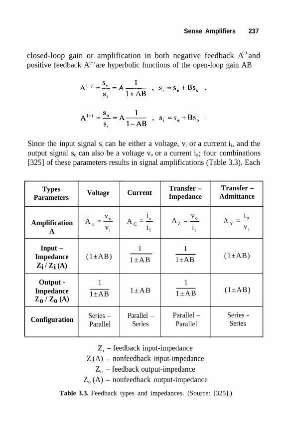
Sense Amplifiers 237
closed-loop gain or amplification in both negative feedback A(-) andpositive feedback A(+) are hyperbolic functions of the open-loop gain AB
Since the input signal si can be either a voltage, vi or a current ii, and theoutput signal so can also be a voltage vo or a current io; four combinations[325] of these parameters results in signal amplifications (Table 3.3). Each
Input – 1 1Impedance (1±AB) 1±AB 1±AB (1±AB)Zi / Zi (A)
Types CurrentTransfer – Transfer –
ParametersVoltage Impedance Admittance
vo io
Amplification A v = A C = voA Z = A Y =
i o
A vi i i i i v i
Output - 1Impedance 1±ABZ / Zo (A)
11±AB 1±AB (1±AB)
Series –Parallel
Configuration Parallel –Series
Parallel –Parallel
Series -Series
Zi – feedback input-impedanceZi(A) – nonfeedback input-impedance
Zo – feedback output-impedanceZo (A) – nonfeedback output-impedance
Table 3.3. Feedback types and impedances. (Source: [325].)
o

238 CMOS Memory Circuits
of the amplifier types, voltage current, transfer-admittance, have differentinput and output impedances Zi and Zo. Impedances Zi and Zo can arbitrar-ily be set by varying the open-loop gain AB. Thus, by increasing AB→∞the input-impedance decreases Zi→0 in both the current- and transfer-im-pedance amplifiers. Furthermore, at expanding AB→∞ the output-im-pedance reduces Zo→0 in both voltage- and transfer-impedance amplifiers.
All four feedback types have importance in designing sense amplifiersto specific memory cells and architectures. Nevertheless, the implementa-tion of the current amplifier results in such a combination of high perform-ance, small layout area and high memory reliability which is difficult tomatch by other approaches in random access memory circuits. The circuitimplementations of current amplifiers may widely vary, and the followingsections discuss the basics of those that have gained applications or havegood potentials for future use in sense circuits.
3.4.3 Current-Mirror Sense Amplifier
The traditional form of the primitive current amplifier is the current-mirror amplifier (Figure 3.45). In the current-mirror amplifier [326], ifdevices M1 and M2 are identical, then the bitline or input current ii is thesame as the readline or output current i , because the gate-source voltageo
V is common for both devices M1 and M2. If M1 and M2 differ only inGS
Figure 3.45. Current mirroring and multiplication.

Sense Amplifiers 239
their aspect ratios W/L otherwise they are identical, then the application ofMOS current equations yields
where β q = β2/β1, β1 and β2 are the respective gain factors of M1 and M2,VDS1 and VDS2 are the respective drain-source voltages for M1 and M2, andλ is the channel-length modulation factor, (W/L)M1 and (W/L)M2 are therespective aspect ratios of M1 and M2, W is the channel width, and L isthe channel length.
Current mirroring and multiplication by βq are implemented usually byshorting the drain and gate of device Ml (Figure 3.46), rather than byusing an extra bias voltage source VGB. An additional device M3 combinesthe bitline selection with the current sense circuit. In this circuit, thecommon gate voltage VGS tends to increase when ii increases. An increased
Figure 3.46. Current sensing combined with bitline selection.

240 CMOS Memory Circuits
VGS, however, reduces the drain-source resistance rd1 in M1, and VGS tendsto decrease. At little changes in V , small variations in current i can beGS i
detected and amplified. The practical limit of the current amplification Ai
is set by the silicon surface area available for the output device M2 whichis determined by the column or by the decoder pitch in most of thedesigns.
Designs for combining high current amplification and small area mayapply a small-size linear amplifier Am between the gates of M1 and M2(Figure 3.47) or a positive feedback. (Sections 3.4.4, 3.4.6, 3.4.8-3.4.10).
Figure 3.47. Combining high current-amplificationand small silicon surface area.
3.4.4 Positive Feedback Current Sense Amplifier
Very small input resistance and some built-in compensation of offsetscan be provided by connecting two identical primitive current mirroramplifiers in positive feedback configuration [327] (Figure 3.48) in whichthe closed loop gain is unity or less. In this configuration when an inputvoltage ∆vi increases, then the input current i i rises and the drain-sourcevoltage VDS becomes greater. Since VDS = V GS in MN2, the increased VGS
tends to increase the current drive capability of M2 and, thereby, todecrease VDS of M2. The current of MN2 is mirrored to MN3, and theeffective gate voltage |VG - Vref| of MP4 grows. Here, VG is the gatevoltage of MP1 and MP4, and Vref is the reference voltage. Nonetheless, alarger |VG - Vref| lowers the drain-source resistances rds of MP4 and MP1,

Sense Amplifiers 241
and thus the gain in both |VG - Vref| and ∆vi get attenuated while aconsiderable current change occurs. Since the closed loop gain is designedto be less than unity, the circuit is stable. To provide the near unity gainand minimum offsets all four devices MP1, MN2, MN3 and MP4 have thesame gain factor β.
Figure 3.48. Simple positive feedback current sense amplifier. (Source: [327].)
The positive feedback, through devices MP1, MN2, MN3 and MP4,transforms the nonfeedback input impedance Zi(A)≈1/gml to the feedback-input impedance Zi;
Using the Thevenin equivalent of this circuit the amplification A may beapproximated by

242 CMOS Memory Circuits
To ensure A<1 over the variation range of transconductances gm-s anddrain-source resistances r -s, and to provide initial bias after selection, and
additional stabilizer bias current source Ibias may be added to the circuit.Here, subscripts 1, 2, 3 and 4 are added to the indices of gm and rd t odesignate transistors MP1, MN2, MN3 and MP4.
The positive feedback in MP1, MN2, MN3 and MN4 results also in anoffset compensation effect. Namely, the feedback mechanism keeps notonly the memory cell generated input voltage swing ∆vi at very smallamplitude, but compensates also the circuit imbalance induced offsetvoltage Voff. Here, Voff is the offset voltage without the positive feedback.To demonstrate the effect of positive feedback on Voff the total of the
Figure 3.49. A complete positive feedback current sense amplifier circuit.

Sense Amplifiers 243
parameter imbalances may arbitrarily be combined in a single term ∆VT,and the offset voltage with positive feedback Voff
(+) can be approximated by
The reduced offset voltage Voff(+)<<Voff allows for sensing of smaller
input signals imbalances, the sensing can start earlier, and the total sensetime becomes shorter.
A complete positive feedback current sense amplifier for staticmemories (Figure 3.49) includes two positive feedback quads M1-M4 andM5-M8, two output transistors for current multiplication M9 and M10, acurrent bias circuit M11-M15 and two bitline load pairs M16-M17 andM18-M19. Although this sense amplifier needs 19 transistors, yet, thetransistors can be designed to near minimum sizes allowed by theprocessing technology. Designs with this circuit benefit in short data senseand transmission times, and in insensitivity to a large range of circuitparameter variations.
3.4.5 Current-Voltage Sense Amplifier
At destructive readout a rewrite capability may be obtained bycombining a current sense amplifier with a voltage sense amplifier so thatthe benefits of current sensing may be retained (Figure 3.50). The current-voltage sense amplifier has two terminal pairs; one of both pairs D- is forread data transfer, while the other pair WR- is for rewrite the sensedvoltage or for write a new datum into the accessed memory cell. A datumgenerated by a memory cell on the bitline pair B- appears as both acurrent difference ∆i = iB and as a voltage difference ∆v = vB - vWhen φ activate both sense amplifiers, and when MT1 and MT2sel and φ'sel
are on, ∆i and ∆v are sensed and amplified by the respective current andvoltage-mode sense amplifier. When the latch in the voltage-modeamplifier takes a stable state, φsel deactivates the current sense amplifier,and on the bitline pair B- the datum appears as a large voltage swing.Consequently, this datum is either rewritten in the accessed memory cell,

244 CMOS Memory Circuits
or replaced by a new datum which may have appeared on the writelinesWR and when MT1 and MT2 are turned off.
Figure 3.50. A current-voltage sense amplifier distributedon the bitline terminals.
Before sensing of a datum this circuit needs precharge and equalizing,which may be implemented either through MT1 and MT2, or through thecurrent-mode amplifier, or by adding extra precharge devices. Theprecharge delay is, usually, timed simultaneously with the word accessdelay, thus, it does not slow the memory operation.

Sense Amplifiers 245
3.4.6 Crosscoupled Positive Feedback Current SenseAmplifier
An elegant implementation of positive feedback and unity gainrequires only four equal sized transistors (Figure 3.51) All transistorsassumed to be identical, and to operate in their saturation regions, andwhen clock φsel turns transistors M3 and M4 on, identical input voltages
Figure 3.51. Crosscoupled positive feedback current sensing circuit.(After [324].)

246 CMOS Memory Circuits
VB = V = VG1 +VG2 appear on the bitlines B and VG1 is the gate-sourcevoltage for both M1 and M3, and V is the gate-source voltage for bothG2
M2 and M4. The input voltage V + VG1 G2 changes very little and only for ashort transient time, when an accessed memory cell induces a currentdifference ∆i between iB and i . The current difference may change VG1
and V in opposite directions, but the feedback at unity gain provides aG2
VG1 + VG2 ≈ Constant for small ∆ i’s. Because iB and i pass throughdevices M3 and M4, a somewhat reduced ∆i appears also on the currenttransporting data lines D and Thus, a current sensing and currentconveyance can be obtained at very little sense voltage variations. Thecurrent sensing and conveyance do not require an extra precharge andequalization because the circuit inherently returns to its equilibrium stateVB = V = V are the voltages on the bitlines BG1 + VG2, where VB and Vand
The analysis of this circuit [324] may be simplified by considering thatthe identical bitline voltages VB = V = VG1 + VG2 cause a virtual shortcircuit between the inputs. This virtual short makes plausible theappearance of a very low input impedance Z i (Table 3.3)
Here, gm is the common transconductance of all devices at the fullybalanced ideal state of the circuit, and indices 1, 2, 3 and 4 designate thegm in transistors M1, M2, M3 and M4. It follows that in the ideal case,when g approaches zero, and ifm1 = gm2 = gm3 = g = gm4 m , impedance Z i
g = g then Z is negative.m1 = g m2 > g m3 m4 i
A negative Z i may cause instability. Stability at little current loss canbe obtained by keeping Zi positive and by choosing the bitline load

Sense Amplifiers 247
resistance RB = R = Z1/2. Using the equation of ZT, the DC stabilitycondition may be expressed as
which indicates the importance of nonzero bitline load resistance.
The presence of bitline capacitance CB= C and dataline capacitanceC may cause signal ringing in the output current iD = C o(t) when anaccessed memory cell generates a rapid input current charge (Figure 3.52).
Figure 3.52. Output current signal as a response to anideal current step on the input.
A simple approximation of the current response i o(t) to an ideal Io-amplitude current step-function with I 1(t) may be obtained by applyingo
the Laplace transformation method, at the assumptions that all parametersare linear, devices M1, M2, M3 and M4 are identical, effects of substrate

248 CMOS Memory Circuits
bias voltages V -s are negligible, and the drain-source conductance of theBS
transistor devices r <<1/g ;d m
where in practice
The equation of i (t) clearly indicates that damped sinusoid currento
swings can appear on the outputs, the swings have a frequency f = ω /2 π,
and the time constant for the switching τ is smaller than the time constant
of the bitline τ = R CB B B. Although a small τ result quick rise and falltimes t and tr , but the total sense delay may be long because of the timef
needed to attenuate the signal swings. The attenuation time T may crudelya
be estimated by T = 5 τ.a
In designs, rather than calculating T , the velocity of transient dampinga
v in the units of N/sec is practical to use. N indicates the time durationtd
necessary to decrease the amplitude of the first overshot I to I /e » I /2.71.1 1 1
The velocity of amplitude damping v can be predetermined bytd
where σ is the real part of the complex root i ρ = σ + jω of the Laplacei i i
transformed transfer function that describes the feedback circuit (Section3.4.10), and σ is a function of g , R , C , R and C and, in a lesseri m B B D D
degree, of other parameters.

Sense Amplifiers 249
3.4.7 Negative Feedback Current Sense Amplifiers
The negative feedback current sense amplifier (Figure 3.53) features smalloffset, small input resistance and small voltage swings [328]. Because thiscircuit amplifies an input current difference ∆ i= iB - i –
B to an outputvoltage swing ∆vo = vo1 - v o2 the circuit, in essence, is a transferimpedance amplifier. For the explanation of the amplifier operation perfectcircuit symmetry is assumed prior to the activation of the amplifiers DA1
and DA2. Both amplifiers DA1 and DA 2 are activated simultaneously whenthe accessed memory cell generates a certain current difference ∆ii. Anincreasing bitline current iB through MD1 would increase the drain-sourcevoltage VDS1 of MD1, but an increased VDS1 creates an increase in the inputvoltage vi1 = VDS1 - Vref on the input node B of the differential amplifierDA1. AS DA1 amplifies this increase in Vi1 , the gate voltage V GS1 of MD1
Figure 3.53. A negative feedback current sense amplifier.

250 CMOS Memory Circuits
increases and, thereby, counteracts the growth in V and v .DS1 i1
Simultaneously, a decreasing bitline current i– through MD2 would causeB
a reduction in input voltage v on node B, but this reduction is lessened byi2
the feedback through DA . While DA and DA2 1 amplifies ∆ i ,v and v2 i i1 i 2
changes little, but the output voltage difference ∆v ,which appear on theo
gates of MDl and MD2, depends on ∆i . Assuming that MD1 and MD2i
operate in the saturation region and that the saturation currents of MD1and MD2 are the same, the current balance may be approximated as
where V and V are the threshold voltages of devices MD1 and MD2.T1 T2
From this equation ∆v is0
The equation demonstrates that the sense amplifier converts ∆ i i to ∆vo witha gain of (2 /β)1/2, and because (2∆ii/ β)1/2 >> ∆V T, the circuit operationsuppresses the ∆VT caused offset.
The effective operation of MD1 and MD2 requires the aid of twoamplifiers DA and DA . Because the implementation of DA and DA
1 2 1 2
requires compromise in silicon area, this circuit may gain applications inmemories where the constraints for sense-amplifier regions are notstringent, e.g., in SRAMs, ROMs and PROMS.
3.4.8 Feedback Transfer Functions
Generally, a feedback sense circuit may be partitioned into a (1) signalgenerator, (2) measuring element, (3) executor element, (4) error signalformer and (5) reference signal generator (Figure 3.54). In this circuitexample, the signal generator is an accessed memory cell and the bitline,the measuring element is a voltage divider, the executor element is a one-transistor current amplifier, the error signal former is a differential voltageamplifier, and the reference signal generator is a voltage divider. Thisseparation of constituent elements, and the presumption that in small

Sense Amplifiers 251
signal sensing the sense circuit operates as a closed loop linear system,allow for the use of transfer functions [329] in the analysis of feedbackcurrent and voltage amplifiers.
Figure 3.54. Separation of constituent elements ina feedback current sense circuit.
A transfer function Y(p) is the quotient of the Laplace-transformedoutput signal So(p) and input signal Si(p) at zero initial conditions:
Y(p) may characterize a complete circuit, a subcircuit or a circuitelement. If the subcircuits or the circuit elements are separated so that theirindividual input/output interfaces do not present any load to each other,

252 CMOS Memory Circuits
Configuration Transfer Function
Series YA (p)YB(p)
Parallel YA(p) + YB(p)
Negative Feedback YA(p)/[1 + YA(p) YB(p)]
Positive Feedback YA(p)/[1 - Y A(p) Y A(p)]
Table 3.4. Basic configuration and their transfer functions.
the unloaded entities can be represented by blocks. These blocks may becoupled in arbitrary configuration. In linear systems, four basicconfigurations series, parallel, negative and positive feedbacks, set thebasic rules for determining Y(p) of complex networks (Table 3.4).
In the following, Y(p) is applied to demonstrate how the bitlinevoltage vB, the output resistance ro, and the stability of a current senseamplifier are influenced by feedbacks. Nonetheless, in the design offeedback sense circuits Y(p) may also be applied in general mathematicaland in specific transient analyses.
3.4.9 Improvements by Feedback
In a parallel-regulated current sense circuit (Figure 3.55a) the effects ofpositive feedback, on the bitline voltage vB and on the output resistance ro,can be shown on the low-frequency equivalent (Figure 3.55b). This lowfrequency equivalent assumes that all circuit elements are characterizableby linear, time-invariant, concentrated parameters, that the transistorsoperate in saturation regions, and the capacitances have no influence onthe control of vB levels and of ro . Although bitline and output capacitancesCB and Co are determinative in the transient behavior of the bitline signalvB(t), the effects of feedback on the basic vB and on its long-term changes∆ vB, and on the basic ro , can be made plausible on a low-frequency modelthat disregards all capacitances in the circuit.

Sense Amplifiers 253
Figure 3.55. A parallel-regulated feedback sense amplifier (a)and its simplified low-frequency equivalent (b).
In the low-frequency equivalent circuit, transfer functions Y(p),YA (p) and YB (p) can be simplified to time-independent terms Y, YA and

254 CMOS Memory Circuits
Y B, and by using the block representation of the circuit (Figure 3.56) thetransfer function of the complete circuit can be expressed as
Y = YA YB /(1+KY A YB ) .
Assuming that voltage divider draws negligible current, the componentfunctions of Y are YA = g m R L, YB = Ro /(Ro +RL ), and K = R2/(R1 +R 2 ).Here, gm is the transconductance of M1, RG is the equivalent generatorresistance coupled to the bitline, Ro is the equivalent load resistance on thesense amplifier output, R1 and R2 are the resistances in the voltage divider.
Figure 3.56. Block diagrams of the parallel-regulated feedback sense amplifier.

Sense Amplifiers 255
The bitline voltage vB as a function of the generator voltage vC andreference voltage VR can be obtained from the equations of Y, YA, YB andK as
A partial differentiation of v B by vc gives the bitline voltage change ∆vB asa function of the generator voltage change ∆vc;
Similarly, the partial differentiation of vB by the output current io providesthe output resistance r o a s
The equation of ∆vB and r o indicate that both the bitline voltage variationand the output resistance of a sense amplifier can significantly be reducedby the application of a feedback.
By the implementation of an additional or double feedback (Figure3.57) with a gain of D, parameters ∆vB and r o may further be improved:
Increasing bitline voltage variations ∆v B -s demonstrate sensitivity of thesense amplifier and allow for early signal detections. Small sense amplifieroutput resistances r o -s decrease the switching times. Consequently,memory access and cycle times can greatly be improved by the use offeedbacks in sense circuits. Feedbacks may be implemented in a greatvariety of parallel and series configurations, but their use in sense circuit islimited by size and stability considerations.

256 CMOS Memory Circuits
Figure 3.57. Double feedback.
3.4.10 Stability and Transient Damping
The application of feedback in a closed loop sense circuit raises thequestion of stability. A closed loop electric circuit is stable, if it is able toreestablish its original equilibrium state by itself after a single event signaldisturbed its equilibrium. In a sense circuit, the single event may be asignal that is generated by the accessed memory cell or a noise signal thatmay be coupled into the circuit through capacitances.
When the sense circuit is described by transfer functions, the criterionof stability is that all real parts σi -s of the roots ρi = σ i + jωi ; of the equation1+Y A (p)Y B (p)) = 0 must be positioned left from the jω axis on thecomplex plane (Figure 3.58), i.e., Repi = σ i <0. Here, Y A (p) and Y B (p) arethe transfer functions of the constituent subcircuits. For certain sensecircuits, an extended stability criterion σ i<∆σ, where ∆σ is a safety amountthat may be imposed to allow time for the attenuation of eventual signalringing (Section 3.4.6).
Stability conditions and signal ringings in sense amplifiers can also beinvestigated, of course, with other well known methods including Ruth-Hurwitz, Mihailov, Nyquist, Bode, Kupfmuller, etc. criteria [330].

Sense Amplifiers 257
Figure 3.58. Root locations at stable operation on the complex plane.(Source: [329].)
3.5 OFFSET REDUCTION
3.5.1 Offsets in Sense Amplifiers
Offset is particular and inherent to differential sense amplifiers, and itis the voltage or current difference which appears between the two outputnode potentials or between the two output currents, when an identical in-put voltage or bias current is applied to the two inputs. The offset voltageor current has to be counteracted by the memory-cell-generated signal forcorrect sense operations. Theoretically, differential sense amplifiers areelectrically balanced symmetrical circuits. In practical implementationsboth the transistors and the passive elements have slight parameter differ-ences in spite of the utmost design efforts to assure their symmetricity.These parameter differences, and the resulting sense amplifier offsets, aredistributed spatially throughout the chips, wafers and lots (Figure 3.59),and the signal generated by a memory cell has to act against and neutralize

258 CMOS Memory Circuits
the appearing maximum offset before the sensing of a data signal couldstart. Thus, the offset limits the sensitivity, i.e., the minimum data signalamplitude that the circuit can detect, and it delays the effective start of datasensing. To improve both sensitivity and sensing speed the offsets shouldbe kept small by minimizing the imbalances between the halves of adifferential sense circuit.
Figure 3.59. A distribution of offsets.
Imbalances may result from the effects of semiconductor fabrication,voltage and current biases, temperature changes, radioactive irradiationsand others, and occur as nonuniform variations in threshold voltages ∆VT,gain factors ∆β, leakage currents ∆IL , load resistances ∆ R , loadL
capacitances ∆CL , transistor inherent gate-drain, gate-source and drain-

Sense Amplifiers 259
source capacitances ∆C GD1, ∆CGS , and ∆C DS , as well as in a variety of otherdesign parameters. A great deal of reduction in parameter variations can beobtained by improvements (1) in processing (e.g., increasing the accuracyof mask alignments, ion implantation dose, plasma etching, ion millings,diffusion control, annealing, etc.), (2) in transistor device and interconnectdesigns (e.g., using environmentally insensitive materials, stable oxide-semiconductor and oxide-polysilicon interfaces, etc.) and (3) in startingmaterial (e.g., eliminating nonuniformities in silicon crystals, avoidinglocalized damages caused by cleaning and polishing, etc.). Despiteimmense improvements in CMOS processing, integrated active andpassive device, and material technologies, the down scaling of featuresizes increases the ratio of the offsets to the data signal amplitudes whichcan be generated by a memory cell in a sense circuit.
Circuit designs can greatly reduce the offsets by (1) misalignmenttolerant layouts, (2) adding offset compensatory circuit elements to thesense amplifier, and by (3) choosing circuits which have inherent offsetcompensation. Because the previous discussion of individual senseamplifier circuits describes also the circuit’s inherent offset reductioncapabilities, where such capabilities exist, the following sections presentthose approaches which use layout and added circuit elements to offsetcontrol.
3.5.2 Offset Reducing Layout Designs
Misalignment tolerant layouts may be designed by dividing thecomponent elements of the sense circuit into subelements (Figure 3.60),and place the subelements as diagonal pairs with reversed drain and sourceelectrodes [331] around a common center point. The division tosubelements and the common centroid geometry statistically average andpartly compensate parameter variations caused by mask misalignmentsand nonuniformities in the transistor pairs. Wide or long transistors laidout in L shapes provide also some tolerance against mask misalignmentsand gain applications in buffer amplifiers.

260 CMOS Memory Circuits
3.5.3 Negative Feedback for Offset Decrease
Sense amplifier layouts may use existing parasitic elements, e.g., wireresistances, Rw and R for offset reduction (Figure 3.61) to implement
Figure 3.60. Division of driver and load transistors.

Sense Amplifiers 261
negative feedback. Resistors R w and R are nearly identical, varyuniformly with environmental changes, and alter independently fromtransistor parameters such as threshold voltage VT , mobility µ, oxidethickness t ox, channel width W and length L, in symmetrical layoutdesigns. A layout design that places the bitlines between the input devicepair M1-M2 and the source device M3, results in individual negativefeedbacks for devices M1 and M2. The feedback modifies the originaltrans-conductance gm to a feedback transconductance g'm as
where R = Rw = R is assumed. If Rg m >>1 then g'm ≈ 1/R, thereby makingg'm in the sense amplifier nearly independent from the transistor parametervariations.
Figure 3.61. Offset compensation by resistances.
Feedback resistance R may also be implemented in forms ofpolysilicon, implanted, diffusion or junction resistors, or in forms of MOSdevices which operate as resistors [319] (Figure 3.62). MOS resistorschange less variably than active MOS transistors do, because duringcircuit operation the bias voltages of MOS resistors change more evenly

262 CMOS Memory Circuits
and, in turn, their threshold voltages and carrier mobilities alter moreuniformly than those of active transistors. The percentage of nonuniformvariations in g m may be calculated by
where, and are the maximum and minimum transconductances,R = r d for MOS resistors, and rd is the dynamic drain-source resistance ofthe MOS device.
Figure 3.62. Negative feedback implemented by serial active devices.(Source [319].)

Sense Amplifiers 263
Other important reasons to implement feedback resistances are todecrease the parameter dependent gain variations and to stabilizeamplification. Assuming that a gain for a simple voltage sense amplifierwithout feedback is A ≈ gm rd, then the gain with negative feedback may beapproached by A ≈ rd /R. This expression of A indicates that R decreasesthe amplification, but the variations in R are much less than in gm and,thus, R can significantly reduce the changes in A also.
3.5.4 Sample-and-Feedback Offset Limitation
Sample-and-feedback circuit elements are applied to compensate largeoffsets in sense amplifiers. Tolerance for excessive offsets may be requiredin memories operating in extreme environments, e.g., radioactiveradiation, very high temperature, etc., or for providing high yield whenprocessing parameters vary greatly.
Configurations of sample and feedback circuits may vary, but theiroperation is based on a common principle [332]. Namely, during initiationa sample is taken from the output nodes (Figure 3.63) by turning feedback
Figure 3.63. A sample-and-feedback sense amplifier. (Source: [332].)
devices MF3 and MF4 on for a very short period of time. When MF3 andMF4 are turned off, the samples are stored on the parasitic capacitanceswhich are present in the gates of regulator devices MR5 and MR6. If the

264 CMOS Memory Circuits
output voltages v01 and v02 are unequal, e.g., v 01 > v 02 , the drain sourceresistance of MR5 rd5 becomes smaller than that of MR6 rd6 i.e., rd6 > rd5,and this tends to equalize v in the01 and v02 as well as currents i1 and i2
sample-and-feedback differential sense amplifier circuits.
Figure 3.64. Sample-and-feedback with offset-amplification in a voltage(a) and in a current (b) sense amplifier.

Sense Amplifiers 265
In this amplifier the nonuniformities of feedback devices MF3 andMF4 are ineffective, because the amplitude V1 of clock signal φF exceedsboth v01 and v02 by more than their bias VBG dependent threshold voltageVT (VBG ). Thus, through MF3 and MF4 no voltage drop can occur, andafter a transient time v01 and v02 occurs also on the gates of MR5 and MR6.Although some additional voltage and current differences may beintroduced by MF3 and MF4, but the feedback reduces this smalladditional offset term together with all other offset causing issues.
The efficiency of offset reduction may be increased by inserting linearamplifiers A1 and A2 (Figure 3.64) into the sample and feedback loop.Because the sample is taken in a much shorter time interval than thetransient time of the feedback operation, the circuit is stable even indesigns which may violate the stability criteria of continuous feedbacksystems (Section 3.4.10). Thus, stability considerations in sample andfeedback circuits do not compromise designs for high amplification andspeed. In random access memories, the time required for offsetcompensation is simultaneous with the decoding delay for word access,and does not occur as an additional delay component. Offset compensatingmay well shorten sense delay times by making possible to detect smallersignals at shorter signal development times. Yet, offset compensationintroduces extra transistors in which should be applied only upon carefulevaluation of the tradeoffs between reduced offsets and increases in powerdissipation and layout area.
3.6 NONDIFFERENTIAL SENSE AMPLIFIERS
3.6.1 Basics
Nondifferential sense amplifiers are those nonsymmetrical circuitswhich detect and amplify signals which are generated by an accessedmemory cell on a single amplifier input node. Topologically,nondifferential amplifiers can not be divided into two mirror-image parts,and their operations and designs are not restricted by offset considerations.Although in a number of applications nondifferential amplifiers havedemonstrated access and cycle times which are competitive with thoseprovided by differential amplifiers, yet, the inherent advantage of

266 CMOS Memory Circuits
differential sensing in sensitivity and noise immunity, leaves only a smallabating segment for nondifferential data sensing.
Historically, nondifferential sense amplifiers have been used to detectand amplify signals provided by nonvolatile memory cells, and tocompensate charge sharing effects by preamplification in random accessmemories. In future CMOS memories, nondifferential amplification mayextensively be applied for impedance transformations, and for signalsensing on long interconnect lines.
Most of the nondifferential sense amplifiers are adopted from analogcircuit techniques. Thus, they may be categorized and analyzed ascommon source, common gate, common drain and combination senseamplifiers [333].
3.6.2 Common-Source Sense Amplifiers
In memories, the basic common-source sense amplifier (Figure 3.65) isusually precharged before its active operation starts on its input, or on bothits input and output, by a precharge voltage VPR. Before the start of theoperation, VPR provides an input voltage vi = VPR that places the quiescent
Figure 3.65. Basic common-source sense amplifier.

Sense Amplifiers 267
operation point Q near to the lower knee or to the center of the linear partof the circuit’s input-output voltage transfer characteristics, where bothdevices, the n-channel MD1 and the p-channel ML2, operate in theirsaturation regions (Section 3.2.1). During a sense operation, the outputvoltage vo increases when vi decreases. At a v i = VPR - ∆v i + VN, where ∆vi
is the change in vi and VN is the cumulative noise voltage, a log.0 can bedetected. A detection of a vI-decrease, i.e., a discharge of the loadcapacitance C L(t), is preferred, because the discharge through an n-channeltransistor is faster than the charge through a p-channel transistor, if theirsizes are the same and their channel length L>0.12µm.
As long as both the n-channel MD1 and the p-channel ML2 operate intheir saturation zones the voltage amplification Av is high. Av may beobtained by using the linear small-signal low-frequency model of thisamplifier as
where g m1 is the transconductance of MD1, rd1 and rd2 are the drain-sourceresistances of MD1 and ML2 respectively. Resistance combination rd1 rd2
and a constant K determine a rather low initial output impedanceZ o(O) ≈ K(rd1 rd2). The input-impedance Zi is very high Zi = vi /IL , becausethe combined amount of the leakage currents IL appearing on the inputnode is very little in small sized sense amplifier devices.
The output-impedance Zo(t) and the load capacitance CL(t) produces a
τ =Z o(t)CL(t) which may be approximated as τf ≈ rd1CL for discharge and
τ r ≈ rd2 CL for charge of CL . The time independent parameters rd1, rd2 andCL may also be used in the operator impedances:
Since the operator impedances used here and in the previous transientanalysis of the bisected simple differential voltage sense amplifier (Section3.3.2.3) are similar, the approximate results obtained for switching timesand delays can be applied also to this common source sense amplifier.

268 CMOS Memory Circuits
A common-source sense amplifier (Figure 3.66), that is used mostly inread-only-memories, includes a drive transistor MD1, a current referencedevice MR2 and current source load devices ML3, ML4. The referencecurrent Iref establishes a gate voltage VGS3 on ML3 and VGS4 on ML4. Dueto V = VGS4 GS3, device ML3 operates as a nearly constant current sourcethat provides a very high virtual load resistance for the driver MD1. Highload resistance results in great voltage amplification Av when MD1operates in the saturation region. Assuming that MD1, ML3 and ML4function in their saturation regions, and that the drain-source resistance rd2
Figure 3.66. Common source sense amplifier used in read-only memories.
of MR2 is linear, and exploiting that the drain currents of MD1 and ML3are the same, the output voltage vo as a function of the input voltage vi
may be estimated by the equation
where β1=β2 and β3=β4 for most of the designs, and parameters β and λ arethe gain and the channel length modulation factors, VGS , V TP and V TN arethe gate-source, p-channel and n-channel threshold voltages, andsubscripts 1, 2, 3 and 4 indicate devices MD1, MR2, ML3 and ML4.

Sense Amplifiers 269
Another four-device amplifier (Figure 3.67) uses positive feedback andself-bias to obtain shorter sensing delays. Prior to a sense operation,control signal φ turns ML4 on, and the feedback through MD2 equalizesthe input voltage vi and output voltage vo, so that v i = vo . When adecreasing vi is generated by a memory cell, φ turns ML4 off, and vo fallsrapidly due to the positive feedback effect provided by the operation ofMD2. The sizes of MD2 and ML4 depend on the speed and loadrequirements, and greatly effect the sizes of MD1 and MD2. Nevertheless,the effective total size of this amplifier is usually small, because it doesnot need extra precharge circuit and because its wiring is simple.
Figure 3.67. Positive feedback and biasing in a nondifferential sense amplifier.
3.6.3 Common-Gate Sense Amplifiers
Common gate amplifiers are applied in random access memories aspreamplifiers or, in more complex implementations, as current senseamplifiers (Section 6.3). The equivalent of a presense circuit thatcomprises a one-transistor common-gate amplifier circuit (Figure 3.68)

270 CMOS Memory Circuits
Figure 3.68. Presense circuit equivalent with a one-transistorcommon-gate amplifier.
includes an input signal generator providing voltage vi , the outputimpedance of the accessed memory cell Zc = rc+1/jωCc, the bitlineimpedance ZB = RB+1/jωCB , an amplifier device MD1, and the inputimpedance of the sense amplifier ZSAi = rSA+1/jωCSA. Here, rc, RB, r SA andCc, C are the equivalent resistances and capacitances of the output ofB, CSA
the accessed memory cell, bitline, and the input of the active main senseamplifier. The common-gate amplifier has a small input impedance Zi, thatcan be calculated by using the low-frequency small-signal model fortransistor MD1 in the equivalent presense circuit, and the analysis of thiscircuit yields
where Rs = R B + rc, and rdl and gml are the drain-source resistance andtransconductance of transistor MD1. Active device MD1 provides also aconsiderable voltage gain Av as indicated by
In the equations of Zi and Av the assumption is applied that MD1 is biasedto operate in the saturation region. The initial bias is imposed by the

Sense Amplifiers 271
The analysis of the common-gate preamplifier circuit may aid thedesign of a charge-transfer preamplifier (Figure 3.69). Although thecharge-transfer and the one-transistor common-gate preamplifiers aresimilar in configurations, they differ in operation concepts. In charge-transfer operation [334], initially, the input capacitance of the sense amp-
precharge voltage V PR. A mid-level VPR may be generated by chargeredistribution on a dummy cell and terminated bitline (Section 4.2.4), anda mid-level V PR provides good amplification for both log.0 and log.1 data.If the detection of log. 0 is sufficient, then high-level VPR can be used inthis circuit.
Figure 3.69. Charge transfer preamplifier.
lifier CSA and the bitline capacitance CB are precharged. CB is much largerthan the input sense amplifier's input capacitance CS A and the cellcapacitance Cc. At to time, capacitance C B is brought through the deviceMD1 to the bitline voltage vB (to) = V G1 - V T(VBG ), where VG1, VT and VBG
are the gate, threshold and backgate-bias voltages of MD1. When MD1turns off, the accessed dynamic memory cell generates a voltage charge,and the potentials of the cell capacitor Cc and the bitline capacitance CB

272 CMOS Memory Circuits
evens quickly, because CC<<CB. At this t1 moment, the bitline voltagevB(t 1) is
After t1, device MD1 turns on, and a current begins to flow from CSA to CB
until time t2. At t2, CB is charged back to the bitline voltage
and the input voltage of the charge transfer preamplifiers vi(t) decreases by∆v ), because at perfect charge distribution the total amounti = vi(to) -vi(to1
of the charge remain the same
Substituting vB(to) and vB(t2) into this charge-equivalence expression, ∆vi
appears to be independent of CB
The voltage change may, however, be slow because the time constant
of the bitline circuit τB is increased by the drain-source resistance of MD1to an estimated
Here, an amplification of the bitline voltage charge occurs during the timet2-to, because vB(t1) is charged back to vB(to) and net charge-change in CB iszero.
Although τ B can be decreased by making β larger, but a large β requireslarge area and that increases the parasitic capacitances in the circuit.

Sense Amplifiers 273
Moreover, the presence of charge amplifiers in the sense circuit can alsoincrease imbalances, magnify offsets and, thereby, reduce sensitivity andoperational speed.
To improve both sensitivity and speed in charge transfer amplifiers,positive feedbacks may be applied (Section 3.3.6.2).
3.6.4 Common-Drain Sense Amplifiers
A common-drain or source follower sense amplifiers (Figure 3.70) isusually applied as impedance transformers to minimize signal reflectionsand as level shifters to adjust signal levels among the operation margins insense circuits.
Figure 3.70. Common drain amplifier.

274 CMOS Memory Circuits
The circuit's low-frequency input-impedance Z is very high, and it isi
determined by the leakage currents between the gate and the ground nodesi LS and between the gate and the supply nodes iLD, and by the input voltagevi ;
The output-impedance Zo may be obtained from the low-frequency small-signal Thevenin equivalent of the common-drain amplifier as
where rd and g are the drain-source resistance and transconductance ofm
transistors, and subscripts 1 and 2 indicate devices MD1 and ML2. Duringa sense operation device MD1 operates in the saturation region while ML2acts as a resistor rd2, and the voltage gain Av is less than unit
To estimate the circuit’s transient switching times, the operatorimpedance Z(p) and the Laplace-transform method may be used so that
and the reversed Laplace transform gives the output current io(t) andvoltage vo(t)
where V1 is the amplitude of an ideal voltage step V11(t) that is applied asthe input signal v (t) to the source follower. From iI = vi o(t) and vsignal fall, rise and propagation delay times, t
o(t) the, may crudely bef , tr and tp

Sense Amplifiers 275
approximated. By applying common-drain amplifiers, short delay times onthe bitlines and wordlines can be obtained, because the choice of an rd2 thatmatches the characteristic impedance of the driven transmission line Z ,o
i.e., Z o ≈ rd2 , can prevent signal-reflections (Section 4.1).

This page intentionally left blank.

Memory Constituent Subcircuits
4
Subcircuits of memories, apart from the memory cells and senseamplifiers, are similar to those component circuits which are used intraditional digital and analog circuits. State-of-the-art requirements incombining very high circuit performances and packing densities,nevertheless, place the constituent subcircuits of CMOS memories inthe forefront of the progress. For CMOS memory designs and analyses,this chapter provides a unique insight to the quasi-stationary trans-mission-line-like behavior of the array wires, to the memory specificaspects of the peripheral circuits, and to the reductions of the harmfulsignal reflections, and distortions, reference- and timing-inaccuraciesand power-line bounces.
4.1
4.2
4.3
4.4
4.5
4.6 Clock Circuits
Power Lines
Array Wiring
Reference Circuits
Decoders
Output Buffers
Input Receivers
4.7

278 CMOS Memory Circuits
4.1 ARRAY WIRING
4.1.1 Bitlines
4.1.1.1 Simple Models
A memory bitline or dataline unites the write-read nodes or the read-only nodes of an arbitrary number of memory cells, and ties them to asense amplifier and to a write amplifier, or to a combined sense-writeamplifier and to precharge devices (Section 3.1.1). At a data-sense or readoperation, an accessed memory cell generates a signal on a bitline (Figure4.1a). The accessed cell may be represented by a voltage or a current
Figure 4.1 Impedance equivalents at read operation (a)and at write operation (b).

Memory Constituent Subcircuits 279
signal generator vg(t) or ig (t) and by a generator impedance ZG or Z’G .Impedance ZL1 that combines the impedances of the decoupler device,sense and write amplifiers and precharge devices terminates one end of thebitline, and its other end is closed by a design- and operation-dependentimpedance ZL2. At a write operation, the write amplifier generates a signalon a bitline (Figure 4.1b). The write amplifier may be modeled bygenerators vg(t) or ig (t) and by an impedance ZG or Z’G. ZG or Z’G iscombined of the impedances of the decoupler device, write and senseamplifiers and precharge devices, ZC is imposed by the accessed memorycell, and ZL2 is the same as that for read operation. In both read and writemodels, the bitline impedance ZB represents the impedances of theunaccessed memory cells and the bitline, and ZB is divided into both partsZ'B and Z"B by the physical location of the accessed memory cell.
The impedance of a bitline ZB that connects n write-read nodes ofaccess devices to memory cells, comprises (Figure 4.10) the distributed
Figure 4.2. Components of a bitline impedance.
resistances of the bitline RB ≈ n x rB and those of the leakage currentpaths R IL ≈ n x rIL; the distributed capacitances of the bitline to other bit-lines CBB ≈ n x c BB, to the ground CBSS ≈ n x c BSS and to the power-lines CBDD ≈ n x cBDD ; the capacitances of the bitline to crossing wordlines

280 CMOS Memory Circuits
Cww = n x c ww , to the gates CBG = (n-l) x cBG and to the sources of theturned-off access transistors CBS = (n-l) x cBS ; and the p-n junctioncapacitances coupled to the bitline Cj ≈ (n +k) x cj. Here, r and c representspecific resistances and capacitances referred to a unit bitline length, andk = 5...12.
In practical implementations the bitline with the unselected accessdevices of the memory cells and with the parasitic elements may bemodelled by lumped circuit elements or by transmission lines [41](Section 4.1.3). Whether a lumped-element or a transmission-line modelshould be used for analysis, depends on the ratio of the rise-time t r a n dfall-time tf to the propagation delay tp of an impulse which is generated onthe bitline-input and which propagates through the bitline. A rule of thumbfor the choice of bitline model is that a transmission-line model should beused if either one of both ratios tr/tp<2.5 or tf /t p<2.5, and lumped modelsapproach the accuracy of transmission-line models if both tr /tp>5 andtf /tp>5.
For first order approximations tr = tf = 2.2 RB CBG and tp = l/ν may beused. Here, l is the length of the bitline, is the propagation velocityof the signal in the transmission line, c is the speed of the light, and εr isthe permittivity. εr ≈ 3.9 for the silicon-dioxide dielectric material that iscommonly used to isolate the bitlines from the other semiconductor, metaland polysilicon materials.
Bitline models which use Π or T type of passive RC networks inladder configurations (Figure 4.3), result increased accuracy approx-imations in computing the switching times tr and tf . In these approx-imations, bitline resistance RB and bitline capacitance CB include all bitlineresistances and capacitances, associated with the bitline (Figure 4.2), andN is the number of Π or T circuit elements used in the model. Byapplication of a ladder made of Π or T circuit elements in a circuit analysisprograms, at N=3 the relative error for the computation of transientresponses can be kept less than 1.1%. Similarly, small error may appearwith the use of the pocket-calculator estimate [42] for t r and tf if opencircuit termination ZL→∞ can be assumed;

Memory Constituent Subcircuits 281
where t0.9 is the time to reach the 90% of the switched impulse's amplitudefrom the time of zero amplitude, rg and cg are the equivalent generatorresistance and capacitance of the accessed memory cell or, alternatively, ofthe write-signal generator. Because RB<<rg and cg<<CB , the reduction ofthe bitline capacitance CB and of the generator resistance rg are theeffective methods to improve switching times tr and tf .
Figure 4.3. P and T type of RC networks in bitline models.
Transmission-line models (Section 4.1.3) allow to predict switchingcharacteristics of bitline signals as function of both the location on thebitline (x) and the time of observation (t), and to investigate the effects ofsignal-reflections caused by the impedances ZG and ZL which terminate thebitline. Signals generated or received on the bitline by different memorycells, travel different lengths x1 and x2 in different times t1 and t2 , and thesignals get reflected differently on ZL1(RL1,CL1), ZL2(RL2
,CL2) and ZG(RG,ZG)(Figure 4.4). Although approximations as RL1 →∞ and RL2→∞ may bejustified; the computations of wave forms, which appear at various bitlinelocations and at diverse time points, are arduous. In a strict sense, themodeling of bitlines by transmission lines is also a simplification, becauseactually electro-magnetic waves are generated in the dielectric materialplaced under the bitline. Nevertheless, the thickness of the dielectricmaterial tox is very small in comparison to the length of the bitline 1,i.e., tox<<1/100, which well warrants the application of the transmission-line theory.

282 CMOS Memory Circuits
Figure 4.4. Different lengths of signal travels in a bitline.
A sense circuit design that has to take the transmission-linecharacteristics of the bitline into consideration, should minimize signalreflections. To minimize effects of the reflected waves on the data signalamplitudes, either a wave-impedance termination of the bitline, or anamplitude clamping, or a timed coupling and decoupling of the senseamplifiers to and from the bitline, may be applied.
A termination of the bitline by a load impedance ZL that is equal withthe bitline's characteristic or wave impedance Z0 results in a zero voltagereflection coefficient ρr = 0, because ρv=(ZL-Zo ) /(ZL+Zo). ZL = Z0 can bedesigned by connecting passive elements parallel Zp and series ZS with theinput impedance of the sense amplifier ZSAi (Figure 4.5). Of course, wave-

Memory Constituent Subcircuits 283
impedance termination can be designed directly as the sense amplifier'sinherent input-impedance. Moreover, the generator impedance of eachindividual memory cell and the terminating-impedance of the other end ofthe bitline may also be designed to be equal with Z to implement a0
reflection-free bitline.
Figure 4.5. Added elements to provide wave-impedance termination.
Reflection caused distortions in data signals may also be mitigated bythe applications of the next described signal limiters (Section 4.1.1.2).
4.1.1.2 Signal Limiters
To limit reflection-caused over- and undershots in the bitline signalv(t) clamp circuits may be used. Voltage clamping may simply beimplemented by (1) clamp diodes and by (2) inverted pull circuits.
Clamp diodes (Figure 4.6a) apply transistor devices MN1 and MN2 indiode configuration and reference voltages V1 and V2. V1, and V2 and thethreshold voltages V ), and through the backgateT (V BG1) and V2(VBG2
biases V BG1 and VBG2 of MN1 and MN2, determine the clamp voltages VC1
and V ). Since theC2, so that VC1>V1-VT (VBG1) and VC2>V2+VT (VBG2
effective gate-source voltages VGS1 -VT (V ) and VBG1 GS2 -VT (V BG2 ) of MN1and MN2 are small, MN1 and MN2 may require large channel widths to

284 CMOS Memory Circuits
provide high currents. Extended channel widths, however, increase bitlinecapacitances.
With the applications of inverted pull circuits (Figure 4.6b) the bitlinecapacitances can be much less than those with the use of clamp-diodes.Namely, clamp transistors MP5 and MN8 can have much larger effectivegate-source voltages VGS5-VT (VBG5) and VGS8-VT (VBG8) and can have, forthe same current, smaller channel widths than diode-devices MN1 andMN2 do. Devices MN3 and MP6 may also be small, because these devicesare used exclusively for under- and overshot detection at the voltagesVD1 ≈ V 1-VT (VBG3) and V D2 ≈ V2+VT (VBG6). The detected and amplifiedunder- or overshot signal turns either MP5 or MN8 on, and MP5 pulls thebitline voltage toward VDD at a signal undershot, or MN8 pulls the bitlinevoltage toward VSS at an overshot. Since at a signal reflection, the currentthrough MP5 or through MN8 may not have sufficient time tosignificantly change the bitline voltage, this circuit may not be able toclamp fast changing signals acceptably.
Figure 4.6. Clamping by diodes (a) and by inverted pull circuit (b).

Memory Constituent Subcircuits 285
A signal clamp circuit (Figure 4.7), implemented by devices RL, MNl,MN2, MP3 and MP4 and by the use of the sense amplifier, may also bedesigned to limit current over- and undershots. Here, current i (t) generatesL
a voltage drop v (t) across the load resistance R . A change in iL L L (t) and,thereby, in vL(t) may alter the gate voltages of the turned-off transistordevices MN1 and MP3. At an overshot MN1, and at an undershot MN3,turns on, and the highly conductive device shunts the input current of thesense amplifier. Devices MN2 and MP4 operate in their triode region toallow for effective regulation of the threshold voltages VT1 (VBG4) andV (V ) can beT3 (VBG3) of the devices MN1 and MP3. VT1 (V BG1) and VT3 BG3
regulated by changing their backgate bias voltages V and VBG1 BG3 throughthe gate voltages V . Voltage and current clamp circuits are seldom1 and V2
used in memories, because reflections can economically be avoided bywave impedance terminations, and the effects of reflections can beminimized by careful timing more effectively at less power dissipationthan that could be done by clamping.
Figure 4.7. Clamp circuit implementation with the use of the sense amplifier.

286 CMOS Memory Circuits
Figure 4.8. Dummy bitline aids timing in an array.

Memory Constituent Subcircuits 287
Careful timing couples the sense amplifier to the bitline when theimpulse generated by a memory cell arrives to the input of the senseamplifier, and decouples the sense amplifier from the bitline before areflected signal can appear on its input. Generally, the signals travel indifferent times from the accessed memory cells to the input of the senseamplifier, because of the different locations of the memory cells on thebitline. To mimic the different signal transmission times and to providecorrect timing for each memory cell location a dummy bitline BD can beused (Figure 4.8). The signal propagation time on BD copies the signaldelays on the bitlines B1,B2,...BN, and tracks the parameter variationcaused signal delay variations as well. When a word decoder signalactivates a word of memory cells, the signal generated by the accesseddummy memory on BD travels to the dummy sense amplifier SAD whichturns the couple-decouple devices MB1,MB2,... MBN on for the time TD.TD is shorter than the signal propagation time between the last accessdevice MAN and the sense amplifier input. On the sense-input capacitorsCi1,Ci2,...CiN trap the signal for the time required for amplification. At theend of time period TD the word decoder deactivates all memory cellswhich are accessible by this decoder circuit. The correct timing for sense-amplifier activation tracks nearly all uniform parameter variations whichoccur in the array.
Signal amplitude variations caused by transmission line effects,i.e., signal propagation time and reflections in the bitline circuit, mayresult in unduly long times for data sensing or in read or write errors.Thus, high speed data sensing may require the use of wave-impedances, orclamping, or activation timing in bitline circuits. In most designs,activation timing is provided by clock signals which are derived from amaster clock, and which activate sensing and other circuit functions inworst-case timing computed by circuit simulation programs.
4.1.2 Wordlines
4.1.2.1 Modelling
A wordline is the low-resistance wire that interconnects the gates ofthe access transistors of memory cells. The memory cells are arranged in a

288 CMOS Memory Circuits
row, and the data set stored in a row of memory cell is called, somewhatmisleadingly although, a word. A wordline circuit includes (1) a bufferamplifier placed between a decoder output and the wordline, and (2) thewordline with its parasitic resistances and capacitances, and, eventually,(3) wordline enable devices and (4) a signal accelerator circuit. In simple
Figure 4.9. Simple equivalent of a wordline circuit.
wordline equivalent circuits (Figure 4.9), the buffers are represented by asignal generator vg(t) or ig(t) and by a generator impedance ZG or Z'G , thewordline is symbolized by ZW and the eventual enable devices, acceleratorcircuit, and any wordline impedance is combined in impedance ZL.
The impedance of a wordline ZW, that ties the gates of n access devices tomemory cells, comprises (Figure 4.10) the distributed resistance of thewordline RW ≈ n x rw; the distributed capacitances of the wordline to otherwordlines CWW ≈ n x cWW, to the ground CWSS ≈ n x cWSS and to the power-lines CWDD ≈ n x cWDD; the capacitances of the wordline to the crossingbitlines CWB = n x c WB, to the channel-areas CWC = n x cWC and to the drainsand sources of n access transistors CWD = n x cWD and CWS = n x cWS.

Memory Constituent Subcircuits 289
Transistor leakage currents from the transistor gates and junction leakagecurrents are negligibly small in most of the wordline circuits. Here, r and cindicates respective specific resistances and capacitances referred to a unitwordline length.
Figure 4.10. Components of a wordline impedance.
A wordline may be modelled, similarly to the bitline models, by pas-sive RC networks (Section 4.1.1.1) and by transmission lines (Section4.1.3). To both the passive RC and transmission line models the equivalentparameters can be obtained by the use of the here-introduced wordline-impedance components (Figure 4.10).
The signals generated by the buffer on the wordline must be fast tokeep access times as short as possible. Signal switching and propagationtimes on the wordline, however, may be long due to the significantcapacitive load and nonzero resistance of the wordline and due to itstransmission-line like behavior. To provide fast signal transients on thewordline, the buffer should switch high currents. Nevertheless, the current-drive capability of the buffer depends on the buffer's size A, and A islimited by the row- or wordline-pitch. Furthermore, an enlargement in Aby a large factor, e.g., 10, over the minimum buffer size A, results in verylittle reduction in signal propagation time t [43] in comparison to ans

290 CMOS Memory Circuits
assymptotic minimum propagation time ts (Figure 4.11). This is mainlybecause the driver’s output capacitance CD gets larger with increasingbuffer sizes, and C adds to the total wordline capacitance CD W . At littleincrease in A and CD, the use of bootstrap buffers or boosting of the word-line can provide fast wordline drive signals, and additionally, avoidthreshold voltage drops (Section 3.1.3.2).
Figure 4.11. Signal propagation time versus aspect ratio and load capacitance.
The wordline capacitance usually kept on minimum by designing theaccess devices of the memory cells to be of minimum gate size. Because ina wordline the gates are connected to each other without contacts tominimize array area, the rather high resistance polysilicon gates are oftenreplaced by or combined with polysilicide and polysalicide materials toreduce wordline resistance.
4.1.2.2 Signal Control
Wordline resistance and capacitance, which appears as a load for thewordline buffer, may be decreased by dividing the wordline into sectorsand shorting the sectors by stripes made of metal or other low-resistance

Memory Constituent Subcircuits 291
material. From the various striping schemas those are preferred whichdivide both the wordline resistance and capacitance as well (Figure 4.12).The efficiency of the division is limited, of course, by the area of the con-
Figure 4.12. Schemas for wordline division.
tacts, and transistors added to the array, by the number of the availableinterconnect layers, and by the effects of the extra capacitances andresistances of the shunting stripes and the transistors and wordline signals.By similar division bitline performance may also be improved.
Further performance increase may be achieved by application of anaccelerator circuit which is placed to the undriven end of the wordline(Figure 4.13). This accelerator circuit amplifies the rising edge of the

292 CMOS Memory Circuits
wordline signal vW(t), and beyond a threshold-amplitude, device MP1provides a rapidly increasing drain current iD1(t) and, thereby, a shorterpull-up time. The influence of signal pull-down times on the wordlines arenoncritical in most of the designs and, therefore, a design with wordlinepull-down acceleration can rarely be justified in CMOS memories.
Figure 4.13. Signal accelerator circuit on the wordline.
Figure 4.14. Application of negative resistance.

Memory Constituent Subcircuits 293
Unconventional memory designs may apply negative resistance -R tocompensate the wordline driver's internal resistance rdr and the wordlineresistance RW in the word-select circuits (Figure 4.14). Combined withwordline capacitance CW resistances rdr and RW are determinative in the
switching times through time constant τ = (rdr + RW) C W. τ can be reduced
to τ = (rdr + RW -R) CW by applying -R. Negative resistance -R can beobtained by numerous methods, e.g., lambda and tunnel diodes (Section2.9.2), but the most amenable ones to CMOS applications are thecrosscoupled inverters.
Figure 4.15. A crosscoupled inverter pair used as negative resistance.
A pair of crosscoupled inverters (Figure 4.15) can provide the negativeresistance -R [44] between nodes and . It is assumed, at to time, thatnode voltages v , where1(t) and v2(t) are the same, i.e., v1( to) = v2(to) = VF
V is the flipping voltage or switching threshold voltage. After tF o, agenerator vg(t) provides a voltage difference ∆v(t) = v1(t)-v2(t) which isamplified by the inverters. This is equivalent with a reduction in thegenerator resistance Rg of the voltage generator vg(t), which means anegative resistance -R(t) between nodes and . R(t) is nonlinear, anddepends on the node voltages v (t) and v1 2(t). With varying voltagesv1(t) and v (t) the charge and discharge currents i1(t) and i2(t), and the2

294 CMOS Memory Circuits
inverter output resistances r (t) and ro1 o2 (t), change as well. For an initialstable state R(t) = ro1 (to ) ro2 (to ) is an acceptable approach. From to ,resistance R(t) can be approximated by piece-wise linear models until t=ts
when the circuit takes a stable state. Between t=to and t=t s , the resistanceR(t) varies considerably, which variation limits the effectiveness ofnegative resistances in the reduction of wordline-signal delays.
Switching times of wordline signals may be reduced, moreover, by theapplication of a negative capacitance -C (Figure 4.16) generated by theMiller effect of a noninverting amplifier AM [45]. Because CMOSoperational amplifiers are slow and require large layout area and power,the use of negative capacitances is very unlikely in wordline circuits.
Figure 4.16. Application of negative capacitance.
Wordline signals must completely turn off the access transistors of thememory cells to minimize the chance of leakage-current caused patternsensitivity. To minimize subthreshold leakage currents, either thethreshold voltages of the access transistors are increased substantially, orthe wordline is kept close to the ground potential by a high-currentwordline-enable transistor during the unselected period of the wordlines.Fast changing wordline signals, furthermore, may induce significantcrosstalking signals (Section 5.2.2) in the long parallel running wordlines.

Memory Constituent Subcircuits 295
Crosstalking may add to the effects of the reflected signals and theircombination increases the probability of multiple selections of memorycells, and aggrandizes spurious currents in the bitline and degradations inoperating margins.
Figure 4.17. Dummy wordline assists timing in an array.

296 CMOS Memory Circuits
The bitlines are separated from the sense amplifiers, and the senseamplifiers are inactive when a wordline turns the access devices of thememory cells on. After the selected row of memory cells generate signalson the bitlines, either a selected bitline is coupled to a sense amplifiercommon to all bitlines, e.g., in SRAMs, or each bitline is coupled to asense amplifier, e.g., in DRAMS, and the sense amplifier or amplifiers areactivated. An early activation of sense amplifiers, however, may result inexcessive power dissipation and in incorrect data reading. To avoid falsereading of data the start of sensing must be timed properly, e.g., by addinga dummy wordline to the array (Figure 4.17). After turning a dummy cellon, the voltage on the precharged dummy wordline changes. This voltagechange propagates with a delay to an amplifier that turns on the senseamplifiers. The delay tracks the uniform device-parameter variations in thewordlines.
Reverse-phased signal reflections in a selected wordline may increasethe drain-source resistances of the access devices or may turn them offbefore the data signals exceed the noise level. Furthermore, over- andundershots appearing in word-select signals may cause excessive hot-carrier emissions, device breakdowns and high level crosstalking.Unselected wordlines may inadvertently be turned on and off by reflectedword-disable signals. Thus, reflections may decrease performance andreliability, or may impair memory operations. Memory designs minimizethe signal reflection or their effects in wordline circuits by applying wave-impedance termination, amplitude clamping and activation timing thesame was as in bitline circuits (Section 4.1).
4.1.3 Transmission Line Models
4. 1. 3. 1 Signal Propagation and Reflections
If the memory design has to take in account transmission line effects,the analysis should be based on the general model of a dx long portion of atransmission line (Figure 4.18) which describes the characteristics of thepropagating voltage v and current i signals by the classic telegraph equa-tions [46]:

Memory Constituent Subcircuits 297
In these equations, Vo is the voltage signal amplitude across Z L ;Zo =[(R+jωL)/(G+jωC)]1/2 is the complex characteristic or wave impedance;ρ=(Z
L-ZO)/(ZL+Z O) is the complex reflection coefficient; γ=±[(R+j ω1)(G+j ωC)]=α+jβ is the complex propagation coefficients; ω=2 πf is the circle-frequency andf is the frequency of a sinus signal; α is the amplitude attenuation and β is thephase factor. R, L, G, C, ZL, Vo, f and l are usually given, thus, by applying theequations of v(x,t) and i(x,t) and Fourier-integration, the voltage and current at
Figure 4.18. Model circuit for a dx long portion of a transmission line.
Here, R, L, G and C are the resistance, inductance, conductance andcapacitance of a dx long increment of the transmission line. For a trans-mission line, that is endless and open in one direction and that is closed bya load impedance ZL on its single end, a solution shows that both thedistance from the line-end x and the time of the observation t aredeterminative in both the voltage v(x,t) and current i(x,t) along the line:

298 CMOS Memory Circuits
any point of time and at any distance from the end as well as parameters ρ andZ o can be computed.
If the wave impedance Z o matches the load impedance ZL , i.e., Zo =Z L ,then no signal reflection occurs, i.e., ρ = 0, the signal energy is absorbedby the load ZL that terminates the transmission line.
If a transmission line would not have any loss, i.e., R = O, G = 0, adigital pulse would propagate along the line without any distortion sinceall of the signals component frequencies would travel with the same νvelocity. In this idealized case neither the wave velocity ν nor theattenuation α depends on the frequency, and for this reason a signal in thelossless transmission-line may conveniently be represented by a Fourier-integral. The Fourier-integral representation of a step function Vo 1(t) is
Since the value of a Vo sinωt signal at an arbitrary x location isVsin ω(t-x/ν) then at arbitrary x after the inception of Vo 1(t) the voltagev(x,t) is
The equation of v(x,t) demonstrates that a step function suffers no distor-tion after any time of propagation in a transmission line that has noresistive and conductive loss.
In case, the line's terminating impedance ZL is frequency independent,i.e., purely ohmic ZL = R, any digital signal is reflected by ZL withoutdistortion and with an amplitude determined by the reflection coefficientρ. Thus a signal at any ρ for any x location at any point of time can beapproximated by a geometric approach which simply sums up thereflections at any point determined by any x and t coordinates (Figure4.19).

Memory Constituent Subcircuits 299
Figure 4.19. Reflection diagram for a lossless transmission line.
For lossless transmission lines which are terminated by purely ohmicimpedances, the voltage reflection coefficient is ρv =(R-Z O )/(R+Z O ), andthe current reflection coefficient is ρi =ρ v ≈ (ZO-R)/(Z O +R). Therefore, ρv = 1and ρ i = – 1 when the line is terminated by an open circuit, and the open linereflects a voltage impulse in the same phase and same amplitude, while itreflects a current input in the opposite phase and same amplitude. Whenthe line is closed by a short circuit the reflection coefficients are ρv = –1 andρi =1 and the reflection phases are the opposite as for an open circuittermination. With ρv and ρ i the amplitude Vo and I o can be calculated forany time t=1/ν and any location x =νt along the line.
If a transmission line is loaded by RL →∞ and the signal generatorresistance R G →0, which may be a crude model for a bitline that isconnected to a voltage sense amplifier, then the full voltage and currentamplitudes Vo and I o , appear in every period of t = 4T (Figure 4.20). Here,T is the propagation time of the wave from one end to the other end of thetransmission line.

300 CMOS Memory circuits
Figure 4.20. Voltage (a) and current (b) impulse reflectionswhen RG →0 and RL → ∞ . (Source [46].)
If a transmission line is coupled to R L→0 and R G →O, which situationmay be applied as an approximative model for a sense circuit applying acurrent sense amplifier, then Vo occurs in every t = 2T, but I o increasesbeyond limits as it should be in an ideal transmission line (Figure 4.21).
Of course, in nonideal transmission lines, where R > 0 and G > 0, theever present losses limit the increase of reflected signal amplitudes and the

Memory Constituent Subciruits 301
idealization of transmission line provides not much more than an insight tothe phenomena occurring in the circuit. Nevertheless, these simplificationsin circuit operation allow for uncomplicated analysis of the phenomenaappearing in high-speed sense circuits.
Figure 4.21. Voltage (a) and current (b) impulse reflectionswhen RG → 0 and R L → 0. (Source [46].)
4.1.3.2 Signal Transients
Transient analyses of signals appearing in transmission lines, whichhave 1 length and which are terminated by a generator impedance ZG andby a load impedance ZL , may conveniently be performed by applicationsof Laplace transforms. By Laplace transforming the telegraph equations(Section 4.1.3.1) at the conditions that initially at t=0 both v(x,0)=0 and

302 CMOS Memory Circuits
i(x,0)=0, the voltage v(x,t) and the current i(x,t) can be transposed to thecomplex p plain as
where
Since parameters 1, Vo , Zo , ZG , Z L and γ as well as the Laplace trans-formed of the practically used generator functions are readily obtainable, theLaplace transformation of v(x,t) and i(x,t) to V(x,p) and I(x,p) is convenient.The reverse Laplace transformation of V (X,p) and I(x,p) to v(x,t) and i(x,t),however, may be difficult; and to alleviate the complications in the analysisthe use of restrictions in the parameters of the transmission line and of theterminating impedances are necessary.
A purely capacitive load impedance Z L = CL can often be used tomodel the input of a CMOS voltage amplifier, and the response signal fora generated voltage step is very important for the design of timing andeventual circuit elements which compensate undesirable signal irregul-arities. For an ideal voltage step v G(t) = V O 1(t) the Laplace transformed isVG (p) = Vo /p, and the operator impedance of a capacitive load isZL (p) = 1/pC L . Combining the expressions of V G (p), and Z L (p) with theequation of V(x,p) and after some mathematical manipulations, the reverseLaplace transform that gives the voltage v(x,t) in four time intervals can beobtained as a function of the location of the observation x, time of theobservation t, input signal amplitude Vo , attenuation factor α, length of the

Memory Constituent Subcircuits 303
transmission line 1, and velocity of the signal propagation v;
The shape of the voltage signal across the load capacitor CL over a time oft = 9T (Figure 4.22) shows over- and undershots. Here, T is the time-period during the signal travel 1 distance.
Figure 4.22. Voltage waves across a load capacitor terminating alossless transmission line.
Signal undershots may also appear when a capacitance CG is dis-charged from a VG initial potential through a transmission line that isterminated by a short circuit ZL = 0 (Figure 4.23) on its other end. With theassumptions of ZG = CG and ZL = 0, the behavior of the bitline circuit of adynamic memory, that consists of a storage capacitor, a bitline microstripand a current sense amplifier, may be approximated.

304 CMOS Memory Circuits
Figure 4.23. Signal shapes when a short-circuit terminated losslesstransmission line discharges a capacitor.
In sense circuit analyses, a resistive generator impedance RG > 0 maybe added to the ideal step-function Vo1(t) generator for improvedapproximation of the delay t , rise td r , fall t t and eventual sap ts times. Saptimes for attenuations of the output-signal swings have to be consideredwhen 0 < RG < Zo (Figure 4.24a), but when RG > Zo the output signal hasno over- or undershots (Figure 4.24b) in a lossless transmission line.
For transmission lines with little losses, i.e., R<<jωL and G<<1/jωC apolynomial approximation to the propagation coefficient γ reveals that thewave velocity v increases with increasing frequencies ω

Memory Constituent Subcircuits 305
but the attenuation α is independent of ω
Figure 4.24. Output waveforms when 0 <RG < Zo (a) andwhen RG > Zo > 0 (b).
The higher frequency components' higher velocity manifests itself ingradual "flattening" of an ideal impulse as the impulse travels away fromthe signal source along the transmission line that has finite but small losses(Figure 4.25).

306 CMOS Memory Circuits
Figure 4.25. Impulse flattening in a transmission line with little losses.
Transmission lines with little losses and with capacitive-resistivegenerator and load impedances, model most of the interconnects, includingbitlines, wordlines and other wires in a CMOS memory chip, acceptably.In interconnect lines, which are plagued with significant losses, as theimpulse propagates away from the generator an exponential decrease inimpulse amplitude adds to the eventual distortions. Significant losses ininterconnect lines, however, are avoided by technological and designmeasures in both on- and off-chip wirings to obtain high operational speedand low power dissipation and little noise sensitivity.
Off-chip interconnects and chip-pins may combine considerable loadinductance L with relatively little capacitive and resistive components.

Memory Constituent Subcircuits 307
Depending on the factor K=Zo/Lv an inductive load on a transmission linemay substantially distort an ideal generator step-impulse (Figure 4.26).
Figure 4.26. Impulse distortion by an inductive load.
The computation of the distortions in an ideal impulse in the generalcase, when all elements R, G, C and L appear in the transmission line andin the terminating impedances, are complex and requires the use ofcomputers. In CMOS memory designs, the use of a general model isseldom necessary. Yet, the modelling of bitlines, wordlines, decoder lines,input and output wirings as lossless and little-lossy transmission lines,i.e., as quasi-stationary electric circuits, is very important to theapproximation of delay and switching times, signal over- and undershotsand general signal forms in CMOS memories which have large storagecapacities and fast operations.

308 CMOS Memory Circuits
4.1.4 Validity Regions of Transmission Line Models
The transmission line models which are widely applied to analyze bit-,word-, decoder-, and signal-lines in a memory chip, include twoimiportant assumptions; (1) the effects of the wire-inductances arenegligible and (2) the propagation time of the signal along a wire of lengthl is constant. While assumption (1) is well justified by the operation andperformance of nearly all implemented CMOS memories, but the validityof assumption (2) to large CMOS memory chips may be questioned [47]because the propagation velocity of the signals depend on the transmissionline's length l, specific resistance r and specific capacitance c, as well as onthe magnitudes of the terminating generator resistance RG and loadcapacitance CL (Figure 4.27). Depending on the parameters l, r, c, RG and
Figure 4.27. Model for determining validity regions.
the propagation of a bit-signal along a wire of length l may be computedby the application of
(a) a synchronous model with constant time irrespectively of l [48],
(b) a capacitive model with a delay increase of log l with increasing l[49],
(c) a diffusion model with a delay increase of l2 with increasing l[410].

Memory Constituent Subcircuits 309
The model to apply for a particular technology and design may bedetermined in a logarithmic diagram (Figure 4.28) where the relativedeviation of the propagation delay ε(γr , γc) from the propagation delaythat can be obtained from the idealized synchronous capacitive modeltp ≈ RoCo(1+γr+γc) is plotted as a function of γr=rl/RD and γc=cl/C L.
Figure 4.28. Validity regions of delay models. (After [47].)
Computations of γr and γ c with parameters of 0.15-2µm CMOStechnologies, results γr r= 10-4…100 and γc= 10- 2…103. These results indicatethat in practical memory designs the long interconnects can be approachedeither by synchronous or by capacitive models.
To operate in the synchronous operating region the design has tosatisfy both conditions for maximum wire length ;

310 CMOS Memory Circuits
where and are the maximum generator resistance and the load capaci-tance, and r and c are the specific resistance and capacitance of the trans-mission line. Expressions for indicate that an operation in the capacitivedelay region can be avoided by designing the wire length l < by sub-dividing the main memory cell array into smaller subarrays, or by theinsertion of repeater amplifiers at fixed RG and CL. In sense circuits, RG,and CL, can be varied only in limited ranges, because the design of thememory cell, bitline and the sense amplifier and the processing technologypredetermine these parameters. Nevertheless, adjustments in the amplifierswhich are coupled to the word-, decoder- and other long lines can well beused for delay time decrease.
For delay reduction in the unlikely case when the transmission linewould operate in the diffusion region the methods described for avoidingoperation in the capacitive region can also be used in addition to theeventual development of integrated nondispersive transmission lines.
The theoretical foundation for the three regions of delay-lengthcomputation (Section 4.13) may be obtained from the definition ofcapacitance and resistance in transmission lines
whence
of homogenous boundary conditions [411]. The final solutions describethe location and time dependency of the voltage v(x,t) and current i(x,t),and an expansion of the propagation delay times t = f(r, c, l, RG, CL) intoTaylor-series assists to obtain the plots of ε(γr ,γc), at the assumption thatboth the driver and driven transistors have the same minimum size. Byincreasing the transistor width, and if width is proportional to the
These are instances for the classical Poisson, or also called diffusion, orheat equations which may be solved by the method of variable separation
p

Memory Constituent Subcircuits 311
capacitive load for all transistors, a nearly constant delay can be ap-proached not only in the synchronous, but also in the capacitive region.
4.2 REFERENCE CIRCUITS
4.2.1 Basic Functions
A reference circuit provides a voltage, current or charge reference levelfor determination of log.0 and log. 1 information when a signal levelgenerated by a memory cell is compared to a reference level by a senseamplifier. In practice, the reference level is a range of quantities ratherthan a single quantity, because of the effects of parameter variationsresulting from the effects of semiconductor processing, supply voltages,temperature and radioactive radiations. These parameter variations influ-ence the operating and noise margins in a sense circuit significantly(Section 3.1.3). To keep the margins wide, either the parameter and refer-ence-level variations should either be minimized, or designed so that thereference tracks the changes of the operating and noise margins, or both.From the plethora of reference circuits, the next sections describe thosewhich have been applied mostly and have future potentials for applicationsin CMOS memories.
4.2.2 Voltage References
Voltage reference circuits, which are applied in most CMOSmemories, include voltage dividers, threshold voltage droppers andcomplex stabilized voltage regulators.
Voltage dividers may be resistive or capacitive. In resistive dividers atprecharge operation a series of resistors (Figure 4.29a) or MOS transistors(Figure 4.29b) charge storage capacitor CL1 to an intermediate referenceprecharge voltage VPR when switch device MS1 is turned on and prechargetransistor MT2 is off. During precharge, when MS1 is off and MT2 is on,reference voltage VR may significantly be subdivided by chargedistribution between CL1 and sense circuit capacitance CL2; and may furtherbe reduced by the threshold voltage VT of precharge device MT2 if thegate-source voltage VGS is designed as VGS ≤ VDS - V T (VBG), where VDS
and V are the drain-source and backgate-bias voltages of MT2.BG

312 CMOS Memory Circuits
Figure 4.29. Voltage dividers implemented in resistors (a) andtransistors (b) provide precharge levels.
Capacitance CL1 are formed preferably of polysilicon lines, which canbe placed underneath the metal lines distributing the supply voltages VDD
and VSS. Transistors MR3 and MR4 can also be positioned under VDD andVSS lines, because they are long and narrow devices. Long divider resistorsR1, R 2, and long transistors MR3 and MR4 allow for increased referencelevel accuracy if they are used with a wide high-current MS1 in thevoltage division, because with long R2, R3, M3 and M4 and with wideMS1 in the expressions of the reference voltages, i.e.,
the resitances R2, R3, rd3 and rd4 have small percentage length-fluxuations,and R are much large thatn r . Here, subscripts 1, 3, and 42, R3, rd3 and rd4 d1
indicate transistors MS1, MR3 and MR4. High-resistance dividersconsume small power, while low-resistance dividers can provide smallervariations in reference level and in precharge impulse amplitudes thanhigh-resistance dividers.

Memory Constituent Subcircuits 313
In a capacitive divider (Figure 4.30), the impulse amplitude obtainedby switching device MS1 is reduced in accordance with the ratio of dividercapacitances CC1 and C C2, and the resulting voltage VR is approximatelyVeventual charge distribution when capacitor C
R = (VDD - VSS) CC2/(CC1 +C C2). At precharge, VR is further reduced by theL3 is coupled to the divider
and, in some designs, by a threshold-voltage-drop through the deviceMT2.
Figure 4.30. Capacitive divider in a reference circuit.
Threshold-drop references use one of the basic characteristics of theMOSFET transmission gate, i.e., the reference voltage V R = VGS - VT (VBG ) ifVGS ≤VD S . VG S , VT , VB G , and V DS are the gate-source, threshold, backgate-bias, and drain-source voltages, respectively. The reference voltage V R maybe obtained directly as a VT drop Figure 4.31a) or as a difference of twounequal V -s in devices MN1 and MN2 (Figure 4.31b). In both cases, theT
voltages VT and VPR follow the on-chip uniform threshold voltage variationswhich may be induced by the effects of semiconductor processing, supplyvoltage and temperature variations, and by certain radioactive radiations.In these simple threshold-drop reference circuits, the effective gate volt-ages [VGS-V T (VBG )]- s of transistors MN1 and MN2, may be small, and thecharge time of capacitor CL , therefore, may be unacceptably slow.

314 CMOS Memory Circuits
Figure 4.31. Threshold-drop references.
Faster charge times and tracking of VT can be provided by increasingV [412] (Figure 4.32). For identical n-channel devicesGS to V GS ≈ 2 VT
MP1 and MP2, at V GS ≈ 2V T the current balance may be approximated as
From the current balance the reference voltage is
VR =VDS ≈VT.
The gate voltage VGS ≈ 2VT is provided by series connected p-channeldevices MP3, MP4, and MP5, when clock φ1 is high and φ2 is low, becauseduring this period the drains of MP3, MP4 and MP5 are individuallycoupled to their own gates by conductive transfer devices. In standbymode, when φ1 is low and φ2 is high, devices MP1-MP5 are biased forradiation worst-case (Section 6.1.2) so that their drains and sources are atVSS and their gates are tied to VDD. The reference voltage isV V, where VR =V DS - V T (VDD,T,RDT ,V BG ) - ∆ T is a function of the supply

Memory Constituent Subcircuits 315
voltage VDD , temperature T, and radiation total dose RDT , and backgatebias V , and ∆V is the error in tracking the threshold voltage VBG T .
Figure 4.32. Threshold voltage change tracking reference circuit.(Source [412].)
Temperature stabilized reference voltage can be obtained from thecombination of a VGS = 2VT biased MOS transistor and negative feedbackcircuit (Figure 4.33). In this circuit [413] the reference voltage V R may beexpressed as
where threshold voltage VT and transconductance gm are parameters of theoutput device MT1, and R is the feedback resistance. VT has negative,while 1/Rg m has positive temperature coefficient. The compounded effects

316 CMOS Memory Circuits
of both the positive and negative temperature coefficients can reduce thetemperature dependency of V R to less than 200 ppm/°C.
Figure 4.33. Temperature stabilized voltage reference.
Generally, increased VR stability for temperature and other environ-mental effects can be obtained by applications of the voltage regulatorprinciples. In a series reference regulator circuit (Figure 4.34), the regulatordevice MRl is placed between the input and the output, the output voltage isdivided by resistors R1 and R 2 and compared to the basic reference signalVB . After a linear amplification the error signal E' is coupled to the gate ofthe executor device MR1, and MR1 counteracts any changes in V R . Thesensitivity S and the output resistance of the circuit Ro may be approximatedfrom the block model of the circuit (Figure 4.35) as
Here, VPR is the stabilized reference output or precharge voltage, Io is theoutput current; r d is the drain-source resistance and g m is the transconductanceof device MRl; A is the voltage gain of the amplifier; and d is the divisionratio provided by resistances R1 and R 2 . By increasing g m, A and d, in
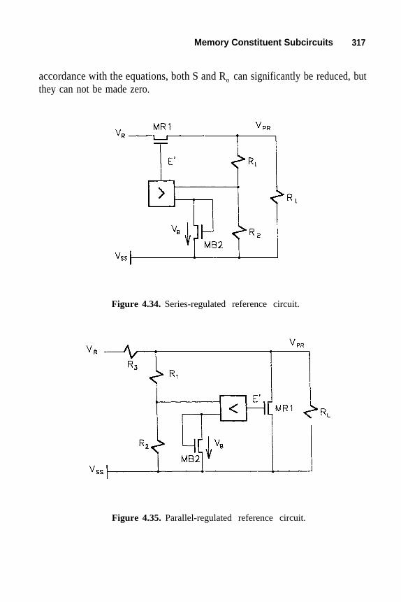
Memory Constituent Subcircuits 317
accordance with the equations, both S and Ro can significantly be reduced, butthey can not be made zero.
Figure 4.34. Series-regulated reference circuit.
Figure 4.35. Parallel-regulated reference circuit.

318 CMOS Memory Circuits
In a parallel-regulated reference circuit (Figure 4.35) both the regulatordevice MR1 and the voltage divider are placed between the output and theground. The difference between the divider's output voltage VD and a basicreference voltage VB provides the error signal E, and E is amplified to E'by a gain of A before it reaches the gate of shunt-device MS1. MS1 drawsincreased current when VR increases, the increased current tend to decreasethe output voltage V ,and vice versa.PR
In the parallel-regulated voltage source, as in the previously outlinedseries voltage regulator, with increasing gm, d and A both the S and Ro maygreatly be decreased and the stability of VPR may significantly be improved.The stability of both the series and parallel regulated reference circuit maybe mathematically examined by application of the Ruth-Hurwitz, Nyquist,Mihailov, Bode, or Kupfmuller methods [330].
Some early designs adopted band-gap reference circuits from thebipolar technology, but bipolar references have seldom been used inCMOS memories, because of the additional process steps required tofabricate bipolar transistors in a CMOS chip and because of their poorvoltage regularity.
4.2.3 Current References
From the wide range of current sources, mostly the current mirror andfeedback type of circuits are applied for current references in sensingschemes.
In current mirror references (Figure 4.36) a simple unloaded chain oftransistors MR1 and MR2 provides approximately constant gate-sourcevoltages VGS1, V GS2 and VGS3. When all devices MR1, MR2 and MS3operate in the saturation region, the output reference current IR0 variesmainly with the current IR2 of MR2, and I R0 changes very little with thealterations of the load current ± ∆IL of source device MS3. The size ofMS3 determines the output current IR0 and output resistance R0 ≈ r d3
(Section 3.4.3). For fast sensing I should be high, which requires a highR0
gain-factor ratio of βq=β2 /β3 and, in turn, a large silicon layout area.

Memory Constituent Subcircuits 319
Figure 4.36. Simple current-mirror reference circuit.
High current ratio IR2/IR0 can be obtained without high gain factor ratioβ by using a modified Widlar current source (Figure 4.37). In this circuit,q
the gate-source voltage of VGS2 of MR2 is substantially smaller than the
Figure 4.37. Modified Widlar current source.

320 CMOS Memory Circuits
gate-source voltage VGS3 of MS3. The high and constant VGS3 provides ahigh and constant output current IR0, as long as all transistors operate in thesaturation region.
Both series and parallel feedback current source circuits (Figure4.38) can be derived from feedback voltage sources (Section 4.2.2) byregulating output currents rather than output voltages. Series and parallelcurrent regulators may be combined for more efficient stabilization(Figure 4.39).
Figure 4.38. Current regulation in series (a) and parallel (b) configurations.
For the feedback current sources, the analysis and design considerationsare the same as for the earlier discussed current sense amplifiers (Sections3.4.3 and 3.4.4) and voltage sources (Section 4.2.2).

Memory Constituent Subcircuits 321
Figure 4.39. Combination of series and parallel current regulation.
4.2.4 Charge References
Charge reference circuits use the principle of charge distribution andredistribution on switched capacitors. In a circuit that contains a finitenumber of capacitors and switches, in absence of generators and powersources, the total amount of charge stored on the capacitors of the circuitbefore the activation of switches ΣQ(t0) equals with the total amount ofcharges after the activation of switches ΣQ(t1) plus the amount of chargeslost during the considered amount of time ∆Q(t1 – t0) i.e.,
Charge distribution and redistribution are widely applied in dynamicdifferential sense circuits (Figure 4.40) to compare data to a referencelevel on a pair of bitlines. In dynamic memories, a binary datum is storedon a cell capacitor Cc, all capacitance coupled to the bitlines CB1 and C B2
are precharged to VPR, and the capacitor of a dummy cell CD is applied as a
Here, vi (t) is the voltage on a capacitor Ci at a t time, and Qi(t) is thecharge stored in capacitor Ci at a t time.

322 CMOS Memory Circuits
Figure 4.40. Charge reference in a dynamic differential sense circuit.
charge reference to generate a reference voltage VR = vD(t1). Here, vD (t) isthe time function of the voltage on capacitor CD . If the time-dependentvoltage on the capacitor Cc is vc (t), the time after complete precharge andbefore turning access devices MC1 and MD2 or is t0, and the time afterturning MC1 and MD2 on and after the complete charge redistribution ist1; then the voltage difference ∆v(t1) between the bitline nodes at the timeof t1 is
Voltage difference ∆v(t1) may be approached by applying the chargeequivalence principle. From the total amounts of charges at the time t 1bitline voltages vB1(t1) and vB2(t2), if zero charge-loss is assumed, i.e.,∆Q(t )=0, then ∆1-t0 v(t1) may be expressed as

Memory Constituent Subcircuits 323
and initially the bitlines are precharged to V P R = v B1 (t o ) = v B2 (t o ). Bysubtracting v ) the voltage difference ∆B 2 (t1 ) from vB1 (t 1 v(t1 ), i.e., thedifferential input voltage for the sense amplifier, can be obtained
where CB = CB1 = CB 2 .
Clearly, a ∆v(t 1 ) ≠0 appears if CC ≠ C D or if vC (t0 ) ≠ vD (t0 ). Thus, themagnitude of either one or both CD and vD (to ) can be used to control thereference voltage V R . In most of the CMOS memories V R is chosen so thatV
R = Q R /CD provides operating margins which are approximately the same
for sensing log.0 and log.1, i.e., V R -VO = V1 -VR . Here, QR is the referencecharge, VO is the maximum of the logic low level, and V1 is the minimumof the logic high level. Knowing VO , V1 , CC , CB and the desiredVR =v(t1 ), and by setting vc (to ) = VD (to ) = VR = VP R ; the dummy capacitanceC D can be approximated. Alternatively, by setting CD = CC the initialdummy cell voltage vD (to ) = V P R can be approached. In designs whereC D ≠ CC , the dummy capacitance is about C D ≈ CC /2. Sense circuits usingC D = CC closely track parameter variations in both C C and MC1, and theyfeature, therefore, higher sensitivity, faster operation and greaterenvironmental tolerance than circuits applying CD ≈ CC /2 do.
One of the primary aims in sense circuit designs is to generate anacceptably large signal ∆v(t1 ) for the sense amplifier. Although theamplitude of ∆v(t1 ) depends mainly on the ratio between CC and C B , anoptimization of ∆v(t1 ) by appropriate charge reference design can signific-antly improve the performance of a dynamic memory.
4.3 DECODERS
The address information to locate memory cells in an array aretransmitted in codes to reduce the number of chip-to-chip and chip-internalinterconnects. The codes applied in CMOS memories are almostexclusively of binary types, because of their area efficiency and theirinherent amenability to memory-array implementations. Nevertheless,

324 CMOS Memory Circuits
some military and high reliability memories may apply other addressingcodes also.
The addressing of a memory cell in a two-dimensional XY array ofn x n = n 2 number of memory cells by the simple binary code needs2 log²n addressing bits and two one-out-of-n decoders. Three one-out-of-ndecoders may be used in very large memory chips in three-dimensionalXYZ addressing schemas.
Addressing decoders, most commonly, are implemented in rectangularNOR and NAND forms (Figure 4.41). In both NOR and NAND decodersthe output lines are precharged by devices MP1 -MP4, while high-resistance leak-transistors MP5-MP8 compensate the leakage-currentcaused changes in logic levels when the decoders are inactive.
The application of a full-complementary decoder (Figure 4.42) isbeneficial, where the row or column pitch allows for accommodation ofdouble amount of transistors, and where low power dissipation and largenoise and operating margins are required. Particularly, memories operatingin radiation hardened or in other severe environments, apply full-com-plementary decoder circuits.
Theoretically, rectangular decoder implementations provide neither thesmallest area nor the fastest operation for one-out-of-n decoders.Nonetheless, the structural similarity between a rectangular decoder and anarray of memory cells, and the adjustability of the decoder output lines tothe row and column pitches of a memory cell array, makes rectangularschemas the smallest and fastest operating decoder implementations tomemory cell arrays.
The implementation of a tree-decoder (Figure 4.43) can providespeedy operation at reduced layout area in some special memories. In tree-configurations, high decoding speed can be obtained because only onethreshold voltage VT drop appears between an input and an output, andbecause buffers may conveniently be inserted in the layout. The layout canbe designed in a small area, because only a single address line, rather thantwo, the true and complement lines, dare needed for decoding, and becauseno drain, source or gate contacts are required to implement the tree circuit.

Memory Constituent Subcircuits 325
Figure 4.41. Rectangular NOR (a) and NAND (b) decoders.

326 CMOS Memory Circuits
Figure 4.42. Full-complementary decoder.
Figure 4.43. Tree-decoder configuration.
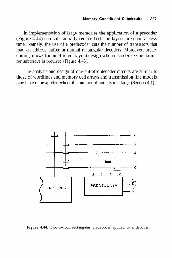
Memory Constituent Subcircuits 327
In implementation of large memories the application of a precoder(Figure 4.44) can substantially reduce both the layout area and accesstime. Namely, the use of a predecoder cuts the number of transistors thatload an address buffer in normal rectangular decoders. Moreover, prede-coding allows for an efficient layout design when decoder segmentationfor subarrays is required (Figure 4.45).
The analysis and design of one-out-of-n decoder circuits are similar tothose of wordlines and memory cell arrays and transmission line modelsmay have to be applied where the number of outputs n is large (Section 4.1).
Figure 4.44. Two-to-four rectangular predecoder applied to a decoder.

328 CMOS Memory Circuits
Figure 4.45. Predecoder enables subarrays.
4.4 OUTPUT BUFFERS
The output buffers of a memory convert the chip internal logic levelsand noise margins to those required for driving the inputs of chip-externalcircuits in digital systems. Memory output circuit operations in certaintemperature and supply voltage ranges, have to satisfy requirements inboth DC and AC conditions, which are specified at the outset of thedesign.
The DC operating conditions of the memory outputs (Figure 4.46)define a minimum output voltage OH (current OH ) for the logic high levelat a given current (voltage), and a maximum output voltage OL (currentÎ OL ) for the logic low level at a given current (voltage). By these outputlevels, the inputs of another integrated circuit have to be driven, and forthe inputs the minimum logic high voltage IH (current IH ) at a given

Memory Constituent Subcircuits 329
current (voltage), and the maximum logic low voltage IL (current IL) at agiven current (voltage), are usually provided. The differences OH - IH
and IL - OL result the margins in which the occurrence of noise signalscan be tolerated.
Figure 4.46. DC output and input logic levels at room-temperature.
The AC operating conditions for the outputs determine the propertiesof the signal-transients which are to be performed by the output buffers atgiven DC signal levels, and comprise the required rise time tr and fall timet f of the output signal when the output pin is connected to a specific loadimpedance. For an output buffer the load equivalent impedance is modeledusually by a capacitive-resistive circuit (Figure 4.47), but modeling forhigh speed operations requires the inclusion of inductive circuit elementsalso.
The primary objective of the output-circuit design is to provide therequired output signal levels for log.0 and log.1 at a switching speedwhich approaches the memory's chip-internal performance, or which

330 CMOS Memory Circuits
maintains a predetermined performance. High speed performance, indriving a large capacitance, can be achieved by applying scaled bufferstages between the wide output devices and the minimum-size chip-interim transistors. Scaling factors may be optimized for speed, power orarea by theoretical approaches [414], but in practice the factorlessbackward-scaling proved to be the most useful approach.
Figure 4.47. Simple output buffer with a load equivalent circuit.
In the application of the factorless backward-scaling technique to thedesign of the simple output buffer, first the size of the two outputtransistors MN1 and MP2 are determined so that MN1 and MP2 arecapable to drive the load impedance with the required fall and rise times tf
and tr . Then, the input impedance of MN1 and MP2 is considered as theload impedance for devices MN3 and MP4, and the sizes of MN3 andMP4 are designed to provide the same tf and tr as the required ones to drivethe chip-external load. The sizes of MN3 and MP4 are smaller than thesizes of MN1 and MP2, because for MN3 and MP4 the capacitive load issmaller than that for MN1 and MP2. Similarly, the sizes of MN5 and MP6are also smaller than those of MN3 and MP4 when they are designed toprovide the same tf and tr on the input impedance of MN3 and MP4. Toapproach the chip-internal tf and tr of minimum sized logic circuits, a

Memory Constituent Subcircuits 331
backward scaling of sizes through three or two stages is sufficient in mostcases.
Output circuit operations often comprise requirements for a high-impedance output-state in addition to provide standardized log.0 and log.levels at certain switching speed. In such tri-state output circuits (Figure4.48) the backward scaling involves the sizing of both logic gates andinverter circuits.
Figure 4.48. Tri-state output buffer.
The operation of complementary inverter circuits include phases whenboth the n- and p-channel devices are turned on. During these phases, theoutput buffer generate noise currents, ground- and supply-bounces, bulk-potential variations and increased substrate currents. To decrease theseundesired currents and voltage changes the output transistor may be turned

332 CMOS Memory Circuits
on during two distinct impulses (Figure 4.49) rather than by a single com-plementary signal.
Figure 4.49. Avoiding direct current between the power supply poles.
The output signal, in numerous applications, is required to stay un-changed on the output-pin until a different datum appears. For that, thedatum may either be stored in a minimum-sized latch placed between thesense amplifier and the output logic circuit, in a positive-feedback senseamplifier in some designs.
Output buffer designs for fast operating systems may have to cope withsignal reflections. To minimize signal reflections the output impedance ZGo
should be the same as the wave impedance of the driven transmission wireZo (Section 4.1.3). Wave-impedances for complementary common-sourceand source-follower outputs may economically be approximated by a seriescombination of a resistor R and a transistor, in which the transistor has avery small drain-source resistance rd <R/k<<Z D, where k = 12-25, so thatR+rd ≈ Zo ≈Z Go . For small wave-impedances, e.g., Zo =50 Ω, this approachmay be impractical, because a small drain-source resistance, e.g.,rd =2.5±0.5Ω , requires the implementation of large p- and n-channeltransistors. Transistor-only drivers providing nearly wave-impedanceoutputs Z Go ≈ rd ≈ Z o can be designed with the application of analog or

Memory Constituent Subcircuits 333
digital control circuits. In CMOS memories the digital control of the outputimpedances is the preferred approach because the economical implemen-tation of its constituent circuit elements is economical.
In an exemplary digital controlled output circuit (Figure 4.50), parallel-connected devices MN1-MN5 and MP7-MP11 determine the outputimpedance Z Go [415]. Devices MN6 and MP12 are replicas of transistorsMN1 and MP7, respectively, and reference impedances Z13 and Z14 aredesigned to approximate the Z13=Z14=Zo condition.The voltage drops on
Figure 4.50. Digital controlled output buffer providing anear wave-impedance interface.
Z13 and Z14 are compared to voltage references in Comparator N andComparator P, and their digital outputs are coded by Encoder N andEncoder P. Depending on the code used, the sizes of devices MN2-MN5and MP8-MPl l may be the same or weighted. Devices MN2-MN5 andMP8-MP11 are activated in agreement with the codes representing the

334 CMOS Memory Circuits
instantaneous voltage drops on Z13 and Z14, so that the combined drain-source resistances of MN1-MN5 and MP7-MP12 approximate the waveimpedance, i.e., rdl-5 ≈ Z o and r d7-12 ≈ Z o , during and after the change of theoutput signal level. Throughout a signal switch either the N-channel or theP-channel output devices are activated. Other variations of impedancecontrolled output circuits may unify the comparators with the encodercircuits, may combine a linear amplifier, a linear integrator with a digitaltime-window quantizer, or may adopt various other design approachesfrom the abundance of digital and analog circuits.
CMOS memory designs may be required to accommodate a simultane-ously operating multiplicity of output buffers to increase the communica-tion bandwidth between the memory and the computing circuits. Simul-taneous multiple output circuit operations greatly enlarge power dissipa-tion and noise generation. A reduction in both power consumption andnoises may be achieved by the applications of low weight codes, most eco-nomically by the implementations of Berger codes (Section 5.7.4.4) to theconsecutive sets of the output data. An encoder-decoder circuit for anN-bit output set (Figure 4.51) may comprise a digital comparator DCOMP,a majority vote logic MVL (Section 5.6.5), an inverting/noninvertingcircuit I/NI, an encoder-decoder circuit for a Berger code ENC/DEC, and aflip-flop FF. The DCOMP circuit compares the upcoming N-bit datavo1(t 1)...voN (t1 ) with the present output data vo1 (to )...voN (to), e.g., by 2-inputXOR gates. Each XOR gate feeds the result of the comparison into theMVL. The MVL circuit indicates the number of output bits which differ attime t1 from those at time to , i.e. ∆N. If ∆N>N/2, then FF generates a flagsignal and the I/NI circuit inverts each output datum, otherwise the outputdata remains noninverted. Thus, the possible number of the output-signaltransitions can be reduced to N/2 or to less than N/2. Further reduction inthe number of simultaneous output-signal transitions are provided by theENC/DEC circuit that encodes the output data-set into a low-weightBerger code (Section 5.7.4.3). If the data terminals are bidirectional,i.e. they serve as both outputs and inputs, then the ENC/DEC circuit alsodecodes the incoming data-set from the Berger code to a weighted binarycode.

Memory Constituent Subcircuits 335
Figure 4.51. Coding schema for N simultaneouslyoperating outputs and inputs.
All three types of output buffer operations, the phase-shifted, imped-ance-controlled and the coded ones, introduce additional delays into thesignal transfer, and require extra silicon area for implementations.Nevertheless, the signal delay extensions and the area increases are smallin many of the CMOS memory designs, and the obtainable combination oflow-power, high-speed and reliable operation greatly outbalances thedrawbacks of the use of complex output buffer circuits. The designs ofoutput buffer circuits for CMOS memories are essentially the same asthose for other digital CMOS integrated circuits.

336 CMOS Memory Circuits
4.5 INPUT RECEIVERS
Input receivers convert the chip-external logic levels and noisemargins to those required to the memory operation chip-internally, andprovide the data signal characteristics which are necessary for the safeoperation of the chip-internal circuits. Prerequisites for circuit designs maybe obtained from the DC and AC operating conditions. The DC operatingconditions for an input receiver require signal-level and noise-marginconversions in the opposite direction to those which are performed by anoutput buffer (Section 4.4). Since the chip-external capacitances coupledto an input receiver are much larger than the receiver’s chip-internal loadcapacitance on its output, the AC conditions and the AC design goals of aninput receiver are also the reverses of those of an output buffer. For theinputs of an input receiver, the worst-case characteristics of the chip-external incoming signal are given, and the receiver has to generate anoutput signal with certain minimum and maximum logic levels, and withgiven rise and fall times, for the chip-internal digital circuits.
Traditional input circuits apply cascaded inverter-chains, in which theinput logic levels and noise margins are adjusted by using substrate biasfor modification of the threshold voltage in the first inverter. Thresholdvoltages may also be adjusted by ion implantation of the channel regionwithout the use of voltage bias between source and substrate nodes.
A differential voltage amplifier (Section 3.3) coupled to a referencevoltage source (Figure 4.52) may also apply nonstandard- often zero-threshold devices for input signal detection. Here, devices MNl, MN2 andMP3 form a low pass filter to avoid detection of spurious signals, and theoutput signal of the differential amplifier is further amplified to providethe required signal levels and transient times.
To those inputs, on which the input signal transients are expected to beparticularly slow, Schmidt triggers [416] may be used to reshape the inputsignal. A Schmidt trigger (Figure 4.53a) is a threshold switch that appliespositive feedbacks selectively to each the rising and the falling signal

Memory Constituent Subcircuits 337
Figure 4.52. Differential amplifier in an input receiver.
Figure 4.53. A Schmidt trigger circuit (a) and the hysteresis curve (b)

338 CMOS Memory Circuits
transient. The selective feedback allows to design the DC output-inputcharacteristics v out =f(v in) of the circuit as well as the forward and reversetrigger voltages VFT and VRT and the hysteresis voltage VH =V FT -VRT
(Figure 4.53b). V FT can be set by the relative sizes of the n-channel devicesMN1, MN2 and MN3, and VRT can be controlled by the sizes MP4, MP5and MP6. When the input voltage vi(t)=0, devices MN3, MP4 and MP5are turned on and the other devices are turned off. Device MN1 becomesconductive as vi(t) rises beyond the n-channel threshold voltage V TN , anddevice MN2 is in cutoff until v i (t)=V FT. When vi(t)>V FT , MN1 and MN2pull the output voltage vo(t) from V DD toward VSS , MP6 lowers vp(t), andMN3 gets less conductive. In turn, the lower vo (t) makes MP6 more andMN3 less conductive. When MN3 is turned off and MP5 is in cutoff,vp (t) is decreased to the p-channel threshold voltage VT P, and the currentthrough MN1 and MN2 results vo(t)=v . Equating the saturationn (t)=V SS
currents of MN1 and MN3, i.e., I1 =I3 , gives an approximation to theforward trigger voltage
and, similarly, to the reverse trigger voltage
where β is the gain factor, and indices 1, 3, 4 and 6 designate devicesMN1, MN3, MP4 and MP6. The expressions of V FT and VRT areapproximation, because they disregard the varying effects of back gatebias voltages, channel length modulations, carrier mobilities, and otherparameters, on the signal development.
For input signals, which are to be stored and reshaped, a level-sensitivelatch (Figure 4.54) can be used. The reference level Vref may be set at TTLlogic threshold V TTL = V ref or at CMOS logic threshold V CMOS = V ref . Clocksignal φA , input voltage v i (t) and V ref control the currents i 1 (t) and i2(t), andi1(t)≠i 2 (t). When φA goes high and v i (t) gets lower, both currents i1 (t) and

Memory Constituent Subcircuits 339
i2 (t) decrease, but the current difference |i 1 (t)-i2(t)| increases rapidly be-cause of the regenerative action of the circuit. When the currents stop thecircuit latches the datum consistent with the input level.
Figure 4.54. Level-sensitive latch.
To avoid reflection by the high input impedance of the input receiverZ i , a chip-external or a chip-internal wave-impedance Zo, that shunts Zi ,may be applied. Z o = Z i provides a reflection coefficient ρ=0 on the inputof the receiver circuit (Section 4.1.3).

340 CMOS Memory Circuits
Input receivers are applied to detect and amplify all type of signalsincluding data, address, control and clock signals. Address input circuits,however, may be required to generate a chip-enable CE signal when atransition or change in the address information occurs and to perform as anaddress transition detector (ATD). A wide variety of ATD circuits can becombined from digital logic gates; yet the economical designs combine theinput receiver with ATD functions and use the static memory cells (Figure4.55) or simple flip-flops which are designed actually for the memory core
Figure 4.55. Circuit combining input receiver and address transition detector.
or overhead circuits. The shown ATD circuit includes an input receivercircuit MN1, MN2, MP3, I1-I5, a memory cell MN4-MN7, MP8, MP9and a one-bit digital comparator circuit MN10-MN13, MP14, I6. The

Memory Constituent Subcircuits 341
input receiver provides the binary address information Ai to both thememory cell and to the comparator in the form of a digital signal that isconverted into chip-internal standards. If the A i signal represents the samedatum as the one that is stored in the memory cell, the potential on the pre-charged node does not change. If the Ai signal does not match thedatum stored in the memory cell, node is going to be discharged, thenew A i information is written in the memory cell, and a chip-enable signalis generated. Nodes CE and may be common to all address inputsA1...A n.
In general, input receiver designs for CMOS memories are similar tothose for CMOS digital circuits, e.g., [417].
4.6 CLOCK CIRCUITS
4.6.1 Operation Timing
In both system and chip levels, memory circuits may be designed tooperate in synchronous or in self-timed (asynchronous) mode.Synchronous design associates sequence and time through the use of asystem- or chip-wide clock signal as a reference. Self-timing does not relyon a reference clock signal, but starts circuit operation when an outputsignal event, which is generated by a circuit, appears in the input of thecircuit under consideration, and concludes circuit oepration when thecircuit under consideration creates its own output signal event that indicatethe accomplishment of the operation. In self-timed designs the outputsignal event initiates the operation of other circuits, while in synchronousdesigns a circuit external clock signal leads the next operation off.
In systems, a memory operates synchronously when a chip enableinput is driven by a central clock signal directly, or indirectly by aderivative of the central clock signal. Self-timing is applied, when a signalchange in the address or data activates the memory without the use of anychip-external clock signal.
Chip internally, most of the memory designs use synchronousdiscipline, because it makes possible to combine high operational speedand clear control on the timing design for the constituent circuits. Self-

342 CMOS Memory Circuits
timed designs may reduce power dissipation, but they are less controllableby available design tools and provide longer memory access times thanclocked synchronous designs do.
Clock impulses which are distributed within a memory chip, may sig-nificantly be delayed (skewed) and distorted due to the effects of the para-sitic resistances and capacitances distributed along the clock lines and dueto properties of the electromagnetic wave propagation in the clock line(Sections 4.1.3 and 4.1.4). Delays and distortions of clocks may be ana-lyzed by lumped resistor-capacitance, transmission-line and diffusionmodels (Section 4.1) to obtain the deviations from intended timing.
Perfect simultaneity in timing within a memory chip can only be de-signed theoretically. In praxis, the design considers the clocking simulta-neous as long as the clock skew does not interfere with the planned oper-ation of the circuit. In memory circuits, approximately equal clock skewsand, thereby, regional simultaneousness, are rather easy to provide, be-cause of the symmetricity of the memory architectures. A double mirror-symmetric architecture is inherently amenable to lay out equal delay pathsfor the clocks when the generator G is placed into the center of the chip(Figure 4.56). If the generated clocks propagate with equal speed in all the
Figure 4.56. Equitime lines in a double mirror-symmetric architecture.

a large memory chip (Figure 4.57).
Memory Constituent Subcircuits 343
four x, -x, y and -y directions, then events of equal delays appear along di-agonal equitime lines T1 , T2 ,… Tn . Equitime lines occur parallel with one ofboth edges of the array, when a synchronized multiplicity of local genera-tors G1 , G2 ...Gk provide clocks to the symmetrically arranged subarrays of
Figure 4.57. Equitime regions in symmetrically arranged subarrays.
Event
Clock
Event Time
Correct Hazard Error
Figure 4.58. Correct, hazardous and erroneous timing.

344 CMOS Memory Circuits
When a subarray, that is placed far from the clock generator, requiresclocking at a certain equitime line Ti the chances are significant that theclock impulse arrives at TI ± ∆t rather than at Ti . ∆ t represents the clockphase shift, that can be so large that the desired event can not be timedsimultaneously with the logic event planned to a certain Ti . Moreover,logic error that result from clock skew may impair the operation of theeffected circuit (Figure 4.58). Therefore, very large memory circuits mayrequire the adjustment of clock phase and establishment of additional"zero" time reference.
4.6.2 Clock Generators
Memory designs use very high number of clock impulses, e.g., 150,for ensuring precise sequence in subcircuit operation, and for carefultiming that facilitates memory operations at worst-case variations ofprocessing and environmental parameters in the chip. Clock generation inthe chip is implemented nearly in all of the designs, because it greatlyreduces the number of chip-to-chip interconnects, makes the complexity of
Figure 4.59. Cascade of inverters in an address transition detector.

Memory Constituent Subcircuits 345
system design acceptable, and can be designed to track the variations ofsome parameters. From the wide variety of clock generating circuitsCMOS memories apply those which base their operation on inverterchains, simple flip-flops or memory cells and a few logic gates. A cascadeof inverters is often used for delay and shaping of signals, e.g., in addresstransition detector (Figure 4.59), and for generation of nearly symmetricaltiming signals, e.g., in ring-oscillators (Figure 4.60).
Figure 4.60. Clock generation by a ring-oscillator.
Arbitrary signal lengths and delays can be obtained by combining set-reset SR flip-FLOPS or memory cells with inverter chains (Figure 4.61).The time delays introduced by the inverter chains and flip-flops, change asthreshold voltage, gain factor, supply voltage and other CMOS deviceparameters vary due to processing and environmental influences. As longas the parameter changes are approximately uniform on the chip, thetiming provided by these circuits adjusts to the changes occurring in theaddressing, data write and read operations. In designs for very fastoperations, some of the inverter chains may be replaced by transmissionlines formed of interconnect lines (Section 4.1).

346 CMOS Memory Circuits
Figure 4.61. Generation of various clock signals.
Clock frequency dividers may preferably be formed of the well knownbinary-counter, shift-register-based nonlinear counter (Figure 4.62), andJohnson counter (Figure 4.63) for divisions by 2n , 2n -1, and n, respectively,there n is the number of stages in the divider. Common features of thesethree frequency dividers are the nearly hazard free operation, the applic-ability of memory cells designed for the data storage array, and smalllayout area.
All clock generator circuits introduced here can apply the memorycells and a variety of repetitive circuit elements which are designedactually for other memory circuits.

Memory Constituent Subcircuits 347
Figure 4.62. Nonlinear counter.
Figure 4.63. Johnson counter.
4.6.3 Clock Recovery
To recover clock-phase shifts and to reestablish timing reference,many memory designs employ simple logic gate combinations, changes inoperation modes from synchronous to asynchronous and back to synchro-nous, and phase corrections by phase locked loop PLL circuits. Apart from

348 CMOS Memory Circuits
the use of traditional logic gate circuits, applications of Muller C, delaymimicking and digital PLL are the most docile approaches to clock recov-eries in CMOS memories.
A Muller C circuit (Figure 4.64) [418], called also as join, last-of, orrendezvous circuit, is a bistable device which provides a log.1 on outputMC only after all the inputs A and B are log. 1, and MC gives log.0 outputonly after all input variables A and B are log.0. The latched outputresponds to the last one of a set of signals changing in the same directionand, thus, it can indicate the accomplishment of a set of logic operations.The indicator signal may be used to start a new sequence of clocks oranother set of operations.
Figure 4.64. Muller C circuit. (Source [418].)
A new sequence of clocks may also be initiated by a delay line thatmimics the worst-case delay of the circuit (Figure 4.65). The delay line ispreferably a replica, or a dummy slice, of a column or a row of thememory cell array or decoder (Section 4.1.1). The dummy elements copythe signal delays occurring in the controlled circuit, and provide parametertracking which assure circuit operation in wide ranges of parametervariations.

Memory Constituent Subcircuits 349
Figure 4.65. Delay mimicking.
Most of the very large memory circuit designs employ phase-lockedloops PLLs to control clock-phase shifts and to reestablish a timingreference. PLL theory and operation are extensively studied [419] andevolved to be an important branch in the communication technology.Albeit PLLs aroused many unrealized expectations, simple PLLs can verywell be used to reduce clock-skews, i.e., to resynchronize clocks. Inmemories PLLs correct clock-skews by exploiting a fundamental propertyof PLLs, that is the capability to adjust the phase of a signal to a referencesignal and to lock the adjusted phase by a feedback loop.
The loop includes a (1) phase detector PD, (2) low-pass filter LPF, and(3) voltage controlled oscillator VCO (Figure 4.66). In simple implemen-tations, the PD compares the digital output signal of the VCO y(t) to adigital reference signal r(t) and generates a digital phase error signale(t) on its output. Phase error signals are separated from their high-frequency components by the LPF. On its output, the LPF provide ananalog voltage signal va (t) that varies its amplitude in correspondence withthe magnitude of the phase errors. The amplitude variations of va (t) tunethe VCO, and the loop locks when both the reference and output signalhave the same frequency and phase.

350 CMOS Memory Circuits
Figure 4.66. Basic phase-locked loop.
In correction of a phase error the loop needs a so-called latency time tostabilize itself. At a signal acquisition, the shape and the timing of theoutput signal may fluctuate without a change in frequency, and this type offluctuation is referred to as jitters. Latency and jitters limit the applic-ability of PLLs in CMOS memories.
Figure 4.67. Primitive phase detection.

Memory Constituent Subcircuits 351
In CMOS implementation, a phase detector may be as primitive as onelogic gate (Figure 4.67), and a voltage controlled oscillator may be asimple ring-oscillator with transistor-capacitor tuning elements (Figure4.68). For designs of low-pass filters resistive-capacitive RC elements inP and T types of ladder configurations can be applied most conveniently,and most of the filters developed in the linear circuit technology [420] canbe adopted to CMOS memory designs.
Figure 4.68. Simple voltage controlled oscillator.
The nearly linear operation characteristics of the CMOS PLL circuits,i.e., for the PD, va(t) = K dt,
2 e(t) for the LPF, Φy = and y(t) = A cos for the VCD, allow the use of analog analysisand design methods. Here, K1, K2, and K3 are circuit dependent constants,Φy and Φr are the phase angles of the output and reference signals, A is theamplitude of the ring oscillator signal and ωF = 2 πfF is the frequency of theVCO at va (t) = 0. The input and output signal frequencies are the same
when the PLL is in locked state, because then is constant

CMOS Memory Circuits352
and Simple CMOS PLLs are so-called second-order analogsystems [421] because their transfer-function H(p) has two poles
where
and represents the frequency in the low-pass filter that isdetermined by the constituent resistive R and capacitive C elements. Fornear optimum operation parameter should be aimed, whichprovides a nonperiodical and fast system transient. The optimization of ξ ,however, is limited by the interdependency of parameters ξ, ωN, ωLPF , K1 ,K2 and K 3. Other system parameters, such as loop bandwidth, attenuationof high frequencies, frequency and phase capture ranges, also imposelimitations and, together with inherent frequency- and phase-noises, coercetradeoffs in PLL designs. Further tradeoffs are introduced by themandatory satisfaction of stability criteria (Section 3.4.10) in the designsof the PLL feedback loop. To alleviate the effects of design tradeoffs avariety of system and circuit technical approaches have been developedand published, e.g., [422], for communication devices.
4.6.4 Clock Delay and Transient Control
Clock delays may be reduced most simply by inserting buffersperiodically into the long clock line (Figure 4.69) [423]. The clock delayTc l on a line that is buffered by single inverters may be approximated as
while Tc l for a line that uses tapered inverters may be calculated by

Memory Constituent Subcircuits 353
Figure 4.69. Single inverters (a) and tapered inverters (b)reduce clock delays (Source [423].)
Here, rt and ct is the total output resistance and load capacitance of a linebuffer output capacitance, ro and co are the output resistance and the loadcapacitance for a minimum size inverter, R1 and C1 are the line resistanceand capacitance, and K is the division factor for a line of L lengths,i.e., L/K is the distance between two line buffers. As a function of K theclock delay T curves minimum (Figure 4.70) because the inverters'c l
inherent delay and their parasitic capacitances counteract the fasterswitching times and shorter signal propagation delays gained by thedivision of lines and by the amplification through the buffers. Thedecrease in delay Tc l depends strongly on the line parameters L, R1 and C1
also, and improvements in clock skews may be little.

354 CMOS Memory Circuits
Figure 4.70. Clock delay as a function of the line division factor.
In addition to clock skews, signal reflections (Section 4.1.3), cross-talkings (Section 5.2.2), ground and supply bounces (Section 5.2.4), maycreate signal distortions which enlarge the voltage- and time-windows forfailures in signal detection. To reduce failure possibility, the clock linesmay have to be terminated by its wave-impedance, carefully shielded byground and supply lines, and reshaped by signal detector and amplifiercircuits. A simple reshaping circuit applies a resistor-capacitor as low-passfilter to smooth out the signal transitions, and a differential amplifier thatswitches logic levels at a reference voltage (Figure 4.71). The voltageamplitude of the clock signal CL may be optimized for minimum delay.
To control the shape and delay of a clock signal a variety of circuitsare developed in CMOS technology, nevertheless, the described circuitsseem to be the most amenable approaches to memory designs. Approacheslike driving the clock network from a multiplicity of pads or driving eachsubarrays by individualized external clocks, can significantly reduce clockskew and latency, but the extension of pin count and system clock networkmay only be acceptable in specific high performance systems.

Memory Constituent Subcircuits 355
Figure 4.71. Clock signal reshaper circuit.
4.7 POWER-LINES
4.7.1 Power Distribution
Power distribution within a memory chip is provided by a circuit oflow-impedance interconnect wires. The nonzero impedance of theinterconnects causes undesired voltage drops (current-resistance IRdrops) on the supply lines, temporary changes of ground and supplyvoltages (ground and supply bounces), appearance of spurious signals inthe supply network (power bus noises) (Section 5.2.4), and electro-mechanical degradations in supply-line materials (electromigration) [424].All these power supply problems and the reduction of their harmful effectsare extensively analyzed in general electronics and integrated circuittechniques [425]. Nonetheless, some techniques are particularly amenableto memory applications.
In memory arrays IR drops may significantly decrease the sense circuits'operating margins, and the currents generated by potential differences inthe power network may oppose the current induced by the datum stored inthe accessed memory cell (Section 3.1.3.3). Thus, the datum may bemisread. To reduce operating margin degradations and misreading

356 CMOS Memory Circuits
probability a Winston-bridge like configuration for power distribution(Figure 4.72) is suggested. In this configuration the voltage drop fromnodes VDD to nodes 1,2,...n are the same as from V to nodes 1', 2',...n' ifDD
the wires have uniform resistance per length unit. Consequently, a voltagedrop V=VDD-V' DD generates no DC current between node pairs 1-1', 2-2'.
Figure 4.72. Power lines in bridge configurations.
Ground and supply node bounces may impose significant reductions inoperating and noise margins, induce substrate currents, disturb both readand write operations, and may cause data loss in memory cells. Each timea memory circuit element changes logic state, a current impulse, mostly asmall one, propagates through the power lines. Large impulses, which arecapable to influence memory functions, can be generated by the outputbuffers, especially when they switch date simultaneously. The outputbuffers with the power lines and package pins, and with all the chip-internal circuits, constitute a rather complex network that can reasonablybe modelled by a combination of transmission lines (Section 4.1.3) andlumped circuit elements. For qualitative analysis, the power supply circuitmay be represented by a concentrated parameter network (Figure 4.73). In
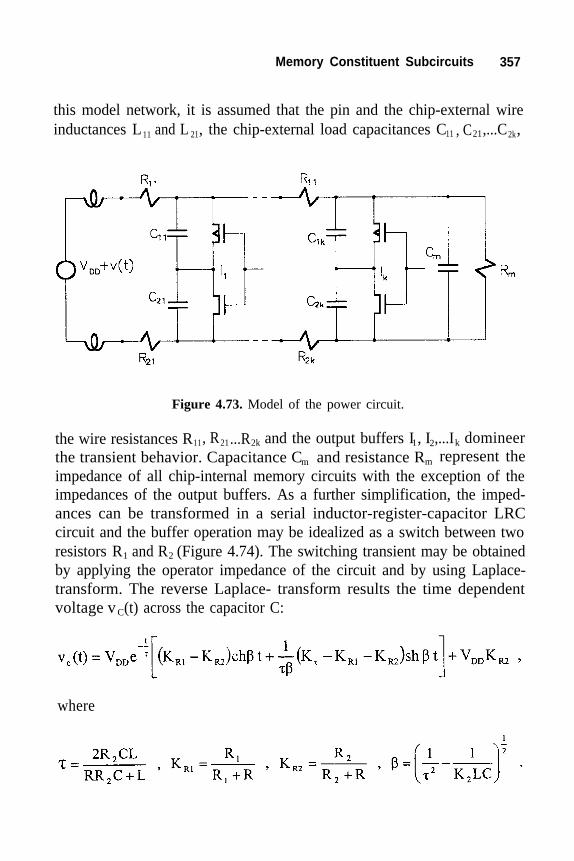
Memory Constituent Subcircuits 357
this model network, it is assumed that the pin and the chip-external wireinductances L11 and L 21, the chip-external load capacitances C11 , C21,...C2k,
Figure 4.73. Model of the power circuit.
the wire resistances R11, R21...R2k and the output buffers I1, I2,...Ik domineerthe transient behavior. Capacitance Cm and resistance Rm represent theimpedance of all chip-internal memory circuits with the exception of theimpedances of the output buffers. As a further simplification, the imped-ances can be transformed in a serial inductor-register-capacitor LRCcircuit and the buffer operation may be idealized as a switch between tworesistors R1 and R2 (Figure 4.74). The switching transient may be obtainedby applying the operator impedance of the circuit and by using Laplace-transform. The reverse Laplace- transform results the time dependentvoltage v C(t) across the capacitor C:
where

358 CMOS Memory Circuits
Figure 4.74. Simplified power circuit equivalent.
The equation of vc(t) describes the approximate signal form that appear inthe chip internal power lines, and indicates the effects of the elements L,R, C, R 1 and R2. Low chip-external inductivity L, small power-lineresistance R, and reduced difference between the on and off resistances R1
and R2 in the output device, decrease the amplitude of the bounce signal.Switching from a small R2 to a large R1 results in a large disturbancesignal. Moreover, this disturbance signal has sinus-hyperboloid comp-onents, and the signal transient rings with β frequency, and the signal
amplitude decreases exponentially with the time constant τ.
In crude approaches, the exponential characteristics can be replaced bylinear approaches, and the signal swingings can be disregarded [426].Presuming that the current signal appearing on the output of the bufferi(t) can be approximated by an equilateral triangle (Figure 4.75), thevoltage signal’s switching or flight time ts is measured from 0.05VDD to0.95V DD, N buffers switch simultaneously and share M ground or supplyconnections, and each of the M ground or supply connections has Linductance and C load capacitance; then the induced noise voltageamplitude VL can be approximated as

Memory Constituent Subcircuits 359
Figure 4.75. Approximation for the shape of the switching current.
The expression of VL indicates that VL, at given inductance L andcapacitance C, can be reduced by minimizing the number of simultaneousdata switches N, increasing the number of ground and supply pins M,extending flight time ts and decreasing supply voltage VDD.
Parameters, L, C, ts, N, M and VDD can limitedly be varied to decreasethe amplitude of the power-line noise VL, because these parameters arerather tightly controlled by the fabrication and packaging technologies,and by the operation, performance and pin-out requirements of thememory. At no effect on technology and at little influence to memorycharacteristics, power line noises can substantially be decreased by carefullayout and circuit designs.
4.7.2 Power-Line Bounce Reduction
Layout designs can effectively reduce ground- and power-line bouncesby keeping apart the output buffers’ power and ground lines and their p

360 CMOS Memory Circuits
and n wells from all the other memory circuits, and by applying multiplepins for the ground and supply connections to the separated output buffersand to all the other memory circuits (Figure 4.76). Furthermore, groundand supply wiring configurations may be designed to establish localcurrent loops for those high-current buffers which are loaded with large
Figure 4.76. Architectures to reduce power-line bounces.
capacitances and inductances (Figure 4.77a) rather than to combine theoutput buffers and loads with the memory-global power route intocommon current loops (Figure 4.77b). Local current loops for the outputbuffers and loads decrease not only the ground- and power-line bouncesbut the switching times of the output-drivers as well. Although, longeroutput signal switching-times may decrease the amplitudes of ground- and

Memory Constituent Subcircuits 361
power-line bounces, output buffer operations with decreased switching-speeds are unacceptable in most memory designs.
Figure 4.77. Designs of output-buffer to power-line connections for localcurrent loops (a) and global current loops (b).
The use of differential sense amplifiers in memories conveys the ideaof the application of differential data processing and differential dataoutput circuits. Albeit the implementations of a symmetrical differentialoutput buffers (Figure 4.78) are costly, because each differential outputneeds two output pads Di and Di, yet in a differential structure the bounce-signals can nearly neutralize each other. Furthermore, the differentialsignal transmission at reduced and optimized amplitudes (Section4.1.1) can greatly improve both speed and power performances.

362 CMOS Memory Circuits
Figure 4.78. Differential output-bounce suppression.
The effects of fast data switching in the output buffers may also bemitigated by reducing the inductances and resistances of the power lines.Namely, both the wire inductance- and resistance-per-unit-length decreasewith increasing wire width, and reduced power-line bounces can beobtained by applying wider power lines. Additionally, wide power lineslessen power-line bounces also by capacitance increase, and reduceelectromigration by lessening current densities.

Memory Constituent Subcircuits 363
The continuous DC current density J, allowed by electromigration maybe computed as a function of the maximum time-to-failure [424]
where factor K A depends on the wire-material's grain size, thermal-gradient and microstructure, N ≈ 1.5 for memory designs, Q ≈ 0.6 eV forpure Al and Al-Si alloys and Q ≈ 0.8 eV for Al-Cu alloys, KB is theBoltzmann constant, and T[°K] is the chip-internal temperature of thememory circuit.

This page intentionally left blank.

5Reliability and Yield Improvement
Reliability greatly effects the application area, environments, andcosts, while yield strongly influences the manufacturing costs ofCMOS memories. Both the reliability and yield of CMOS memoriescan highly be enhanced, in addition to various circuit and processtechnological approaches, by implementations of circuit redundancies.For CMOS memory circuits the issues; how redundancy effectsreliability and yield, what the principal noises, failures, faults anderrors are, what methods can be applied to control noises, reducefailures, repair faults and correct errors, how much redundancy isneeded, and how to obtain fault-tolerance by fault-repair and errorcontrol code implementations, are described in the present chapter.
5.1 Reliability and Redundancy
5.2 Noises in Memory Circuits
5.3 Charged Atomic Particle Impacts
5.4 Yield and Redundancy
5.5 Fault-Tolerance in Memory Designs
5.6 Fault-Repair
5.7 Error Control Code Applications in Memories
5.8 Combination of Error Control Coding and Fault-Repair

366 CMOS Memory Circuits
5.1 RELIABILITY AND REDUNDANCY
5.1.1 Memory Reliability
Memory reliability R(t) is expressed by the probability that the memoryperforms its designed functions with the designed performance characteris-tics under the specified power-supply, timing, input, output and environ-mental conditions until a stated time t. Commonly, the reliability as afunction of time R(t), at given conditions, is expressed by the cumulativedistribution function, i.e., the probability of failure prior to some t time F(t);by the density function of the random variable time-to-failure f(t); by thehazard rate, i.e., the limit of failure rate when the time interval-length ∆tapproximates zero, h(t) ∆ t → 0; and by the mean-time-to-failure, i.e. the averagetime to failure, MTTF [5l]:
Failure, here, means an inability to perform a designed function or a para-metric characteristic under the specific conditions the device is planned tooperate.
The MTTF for a device may be computed through the failure rate λ(t).For λ (t) the definition is
where t1 and t2 gives the start and the end of the time interval ∆t = t2-t1, andR(t ) are the reliabilities at t1) and R(t2 1 and t 2 times. If the failure rateλ (t) represents the number of expected failures over a time interval ∆ t ,then

Reliability and Yield Improvement 367
Failure rates λ(t)-s vary with the time of device usage t as the traditional"bathtube" curves indicate (Figure 5.1). The shapes of the bathtube-curveschange with the level of stress. Nevertheless, for each stress level, all ofthe failure rate curves have (1) an initial rapidly decreasing part thatrepresents infant mortality, (2) a central constant segment that correspondsto the useful device life, and (3) a final increasing portion that implies thewear-out in advanced age.
Figure 5.1. Failure rates versus time at various stress levels. (After [51].)
For any of the three portions of a bathtube curve, parameters R(t), λ(t),h(t), MTTF, etc. can be modeled by discrete and continuous standardstatistical distributions. The generally applied statistical distributions arethe binomial, Poisson, Gaussion, gamma, Weinbull Erlang, long-normaland exponential distributions.
In memory technology the exponential distribution is the most simpleone to use, because the infant mortalities can be eliminated by burn-in andscreening procedures, and both the hazard and failure rates, h and λ, can be

368 CMOS Memory Circuits
approximated by constants. With the exponential assumption and withconstant hazard and failure rates the reliability R(t) may be approximated as
Although these approximations are questioned by some, it has beenshown that they are adequate for reliability estimates of digital memories.
Generally, memory reliability at a set of operating and environmental isexpressed as a triplet of number-ranges representing (1) the confidence level,(2) probability and (3) reliability parameters, e.g., with a confidence of0.82±0.08, the probability is 0.9±0.1 that the lifetime of a 64-Mbit staticmemory is 2±0.2 years in a satellite on a geostationary orbit. CMOSmemories and their constituent circuits, however, are often represented bydoublets: (1) the fraction of the total number of structures, memories,memory arrays, subcircuits, bits, memory cells, etc.; and (2) the (rangeof) values of the reliability parameter (mean-time-between-failures (MTBF),mean-time-between-errors (MTBE), soft error rate (SER), time-to-failure(TTF), failure-in-time (FIT), average failure-rate, mean up-time, percentageup-time, etc.), e.g., the MTBF of a 256-Mbit dynamic memory CMOS arraywith built-in error correction is greater than 500,000 hours. Determination ofreliability differences between two memories or constituent circuits can onlybe made if one of both doublet components is the same, and the assumedoperating environments are also the Same for the compared memories orconstituent circuits.
Modeling of memory reliability is somewhat less complex than that ofdigital logic circuits, because in memories logic-state transition-rates varymoderately, rather than extremely as in logic circuits do. Nevertheless,reliability estimates for memory circuits, with better than first orderaccuracy, require the extensive use of computer programs, which are basedon intricate, mostly on Markovian discrete-state continuous-time, models[52]. At the choice of reliability programs and models the designer shouldweigh the accuracy against the cost-effectiveness of model tractability. This,in turn, depends on the model's complexity for fault and recoverysimulations, technique of numerical approximation to solution, requirementsfor computer operating system, output data, etc.

Reliability and Yield Improvement 369
Explicit reliability data are needed to consider the effects of fabrication,transportation, storage, hot-carrier emission, oxide wearout, electrostaticdischarge, electromigration, latch-up, mechanical stress, corrosion, radio-active radiations and others in the memory circuit design. For circuitreliability simulation a number of simulation programs [53] are available inwhich a variety of failure-causing phenomena can be analyzed separately orcombined by a multiplicity of models.
5.1.2 Redundancy Effects on Reliability
Apart from the conventional measures in design, fabrication andapplication, memory reliability can be improved by the application of someform of redundancy. The term "redundancy" probably was first used ininformation theory in 1920 by Nyquist, who referred to a "useless" sinusoidcomponent signal that "conveyed no intelligence" as redundant. In CMOSmemory technology, however, "redundancy" designates circuits which areadded to the memory to repeat data storage, access, write, read and other orall memory functions, or to implement error detecting and correcting codesfor the improvement of reliability and, what is more, fabrication yield.
A reliability improvement (insurance of operation) can be gained byadding only a limited amount of redundant elements. Beyond a limit, wherethe reliability increase is balanced by the reliability loss due to the inflatednumber of elements in the memory, a reliability decrease (nuisance) appears.In monolithic CMOS memories reliability improvements are restricted bycompromises in silicon surface area speed, and power to much less amountsof redundant elements than reliability could be limited by the number ofelements for the insurance-nuisance equilibrium.
Redundant elements can be applied to the memory in active or standbymodes.[54] Active redundancy that duplicates a circuit (Figure5.2a) improves the reliability of the nonredundant circuit R(t) to thereliability of the duplicated active circuit R DA(t) as

370 CMOS Memory Circuits
while the reliability of a circuit duplication RDS that uses the redundantcircuit in standby mode (Figure 5.2b) may be calculated as
The probability of success for active triplicate redundancy in a majoritydecision configuration (Figure 5.3) RT(t) when all three circuits areactive is
Figure 5.2. Active and standby mode redundancy by circuit duplications.

Reliability and Yield Improvement 371
Figure 5.3. Redundancy by active circuit triplication.
The reliability of a memory that is composed of n identical and inde-pendent circuits, and m or more of the n circuits must be functioning toprovide memory operations, may be expressed by the elementary n-modularredundant model RNMR(t) as [55]
If n-1 of n identical components maintained failure-free in standbyposition, and one of the n-l components can be switched into operatingwith no cost associated to the switching, and if all n components have a

372 CMOS Memory Circuits
constant failure rate λ , then the simple n-modular standby redundant modelR NSR(t) with n-stage Erlang distribution may be applied;
In applications of redundant memories, the probability that the memoryoperates as designed at time t, called the instantaneous availability A(t), inpresence of repairs [56]
is a more descriptive reliability parameter than R(t) alone. Here, M(x) isthe expected number of repairs in the time interval [0,x]. In the absence offailure reparation, A(t) becomes A(t) = R(t).
Estimation of reliability parameters R(t), A(t), etc. for systems hasevolved as an important branch of mathematics, and many of the computerprograms developed for systems can well be applied for analysis of memoryreliabilities.
The rather simple analysis of R(t) and A(t) indicate clearly that thememory reliability can be improved without the use of redundancy byreliability increase of the constituent memory circuits and by the use of cert-ain amount of redundant elements to repeat memory functions.
For reliability improvement on-chip redundancy is rarely employed onthe chip of commercially applied memories, but commercial memories oftenincorporate redundant elements for yield increase. Generally, the extent ofon-chip redundant elements in commercial memories is constrained by cost-effectiveness, yield and performance considerations, rather than by errorrates acceptable in commercial computing and communication systems.Space, military as well as avionics, automobile, and industrial systems,however, demand strict reliability parameters, e.g., life time of 10 years,MTBF of 500,000 hours, etc., which are unlikely to satisfy without the use

Reliability and Yield Improvement 373
of redundant elements in addition to the use of worst-case statistical designapproaches and to the tight control of CMOS parameters.
In addition to design and processing measures high reliability applica-tions require redundancy in CMOS memory circuits. Redundancy in amemory chip is used mostly to implement (1) error detecting and correctingcodes through added memory cells and control circuits, and (2) fault repairby using spare circuit elements and control circuits. The use of error controlcoding and fault-repair circuits greatly depend on the required and on theprimary memory-inherent reliability and yield parameters. Reliability pa-rameters of CMOS memories are influenced by the susceptibility of theircomponent circuits to noises, hot charge-carrier emissions, impacts ofcharged atomic particles, thermal conditions, mechanical shocks, chemicalerosions, radioactive radiations, and by the sensitivity to the other pa-rameters which generally affect the functions of CMOS digital and analogcircuits.
From the large variety of events affecting CMOS circuit reliability thefollowing discussion includes three items; (1) noises, (2) impacts of chargedatomic particles and (3) radioactive radiations, because their effects and thesuppression of the effects may be specific to CMOS memories. Furthermore,for those memory designs in which reliability or yield (Section 5.4)requirements may not be satisfied by direct circuit design, fabrication andhandling approaches, the reliability and yield improvement by employingmemory-global fault-tolerance features is described (Sections 5.5-5.9).
5.2 NOISES IN MEMORY CIRCUITS
5.2.1 Noises and Noise Sources
Noises are unintentionally generated spurious signals which may causeerrors in memory functions by temporary operating margin reductions,incorrect reads, writes and addressings, and by upsets of data stored inmemory cells and of data processed in sense and peripheral logic circuits. Inencapsulated chips, memory circuits may pick up noises from chip-internaland chip-external sources (Table 5.1).

374 CMOS Memory Circuits
Noises
Chip-Internal Chip-External
CrosstalkingPower Supply
Thermal
ElectricalMechanical
ElectromagneticRadioactive
Table 5.1. Chip-internal and chip-external noises.
Since the noise signals, which are generated in CMOS memories by chip-external sources, can be perceived and analyzed the same way as in allother types of integrated circuits, this section focuses exclusively on thememory specific chip-internally generated noises.
Chip-internal noises occur due to capacitive couplings (crosstalk orinduced noises), due to the nonzero resistance and inductance of powersupply wires (power line noises), and due to the thermal fluctuation ofdiscrete electronic charge elements (thermal noises). Noise couplings byinductive elements inside a memory chip is very small.
In a memory chip noises behave stochastically, yet the characteristics ofcrosstalk and power line noise signals are predictable.
5.2.2 Crosstalk Noises in Arrays
Crosstalk or induced noises appear when a signal of memory operationaffects also circuit nodes other than the intended ones through a variety ofcoupling mechanisms, mainly through capacitive couplings. The largestcapacitive couplings are among the bitlines, wordlines and decoder lines. Inmemory cell arrays parallel bitlines are placed perpendicularly to parallelwordlines, while in decoders the parallel input lines and the parallel outputlines are laid out rectangularly.

Reliability and Yield Improvement 375
The capacitive network of these parallel-rectangular structures (Figure5.4) may be simplified for approximate computations by considering that thecapacitances between direct neighbor lines dominate, i.e., Ci j >>C i k andC ik>>C i l, by applying that capacitances Ci j=C jk, C iG =C jG , C i X =C jX, etc., and byexploiting that the crosstalking from useful signals in wire X to lines h, i, jand k may be separated from the crosstalking among the parallel wires h, i, jand k. The capacitance between a signal-wire and the ground or the powersupply CiG combines parallel with the crossover capacitance CiX when thewire X is on ground or on supply voltage potential.
Figure 5.4. Crosstalk capacitances in a memory array.
Although the presence of capacitances among the wires is the cause ofcrosstalkings, neither the amplitudes nor the time-spans of the induced noisesignals depend solely on the capacitances, but also on the impedances of the

376 CMOS Memory Circuits
circuits coupled to the ends of the lines Zi and Zo , on the resistance of theline R and, of course, on the waveform of the generator signal vg (t) driving asignal line. Long lines in a memory array may also operate as transmissionlines or microstrips. For line-to-line crosstalking analysis is sufficient, inmost of the memory designs, to use a model (Figure 5.5) that includes three
line effects. In the Π and T networks, the appropriately divided values of theline capacitances and resistances, e.g., Ci j (C i j1, C i j2, C i j3, C i j4), Ci G (C i G1 , C i G 2,Ci G 3 , Ci G 4 ), C i X (C iX 1 , C i X 2 , Ci x 3 , Ci x 4) and R (R1 , R2 , R3 for line i, have to beapplied, while impedances Zi , Z’i , Zo and Z’o terminate the lines andgenerator vg(t) drives the selected line in the array circuit.
Figure 5.5. Model circuit for crosstalk analysis in an array.
To make plausible the effects of the dominating circuit elements on thecrosstalk-signal a rudimentary model (Figure 5.6), which integrates theeffects of Z i, Zo , R, Ci G and Ci X and of the generator signal vg (t) into thegenerator signal v ′g (t); treats Ci j as the coupling capacitance C ′; combines
Π or T linear passive resistor-capacitance networks to model transmission-

Reliability and Yield Improvement 377
Figure 5.6. Rudimentary model for crosstalk-signal demonstration.
Ζ′i , Ζ′o and R in R′ , and disregards Cj G and Cjx ; may be applied. Assumingthat an exponential vg (t) appears in line i
Here, Vg is the amplitude of the signal generated on line i, and τ g is thetime constant of the generator circuit determined by the impedances of thedriver of line i and of the elements connected to line i. In this rudimentarymodel circuit, the Laplace-transformed of the voltage signal across R′,i.e., of the crosstalk signal, may be gained as
transformation gives the time function of the crosstalk signal on line j aswhere τ′=C ′R′ and R ′=f (Z′ i , Z′o , R). From VR (p) an inverse Laplace-

378 CMOS Memory Circuits
The expression of vR(t) clearly shows that the crosstalk-signal amplitude
and waveform (Figure 5.7) depend on both τg and τ' and, through those,
of all capacitances and resistances of the wires, drivers and terminating
circuits. If in this circuit τ '<<τg, Vg <<VDD and VDD is the supply voltage,
then the amplitude of the crosstalk signal is small. A small τ' can beobtained by creating small line-to-line capacitance Ci j , large line-to-ground(line-to-supply) capacitance Cj x , small line-to-ground (line-to-supply)terminating impedances Zi, Z'i and Z o , and small line resistance R. A large
τ g is undesired, because it would slow the operation by the effects ofimpedances Zi and Z o , resistance R, and capacitances CiG and C i x . Line-to-line capacitances are controlled, most often, by limiting the lengths ofparallel running-signal lines, and by decreasing the fringing capacitances
Figure 5.7. Crosstalk signals.

Reliability and Yield Improvement 379
signal delays and elevated power dissipations.
of the wires. Inasmuch as fringing capacitances determine line-to-linecapacitances, the process technology has to aim to reduce the thickness ofthe conductors and to optimize the layout rules for acceptable crosstalkingrather than for minimum area or for maximum speed conditions.
Improvements in both noise signal amplitudes and speed can be obtainedby coupling drivers with low output resistances and receivers with smallinput resistances to the effected wires. Designs of low resistance drivers andreceivers require wide transistors, yet the widths may be bounded by circuitarea restrictions, e.g., row or column pitch. The general avoidance of “float-ing” circuit nodes, i.e., drain, gate, or source nodes which are disconnectedfrom ground or supply lines, and the use of low-impedance sense amplifiersand line-buffers, are vitally important to keep chip-internally generatednoises on small levels in high-density memory circuits.
Noise reduction can also be provided by passive shielding that protects awire from the other ones' electric fields. Nonetheless, the passive shieldingof electrical fields may require extra space, often increases processcomplexity, and the increased wire-to-ground capacitances may cause longer
5.2.3 Crosstalk Reduction in Bitlines
Particularly noise-prone is the read signal on the bitline in high-densitymemories. Although the folded bitline design exploits the high common-mode-rejection-ratios of the differential sense amplifiers, the capacitive cou-pling between the bitlines of neighbored sense amplifiers can pick up sig-nificant amount of noise signals through wire-to-wire capacitances, e.g., Ci j
(Figure 5.8).
Significant reduction in noise coupling can be achieved by inter-digitizingthe bitline structure (Figure 5.9). In the interdigitized structure, when a senseamplifier SAi is activated, SAI’s mirror symmetric counterpart SAj is pas-sive, and the bitline pair connected to SA j is tied to a supply pole throughsmall resistances. The bitline pair of SAj shields and greatly reduces theeffective capacitive coupling between SAi and SA j, but increases the activebitlines cumulative wire-to-ground (supply) capacitances.

380 CMOS Memory Circuits
Figure 5.8. Wire-to-wire capacitances in a bitline circuit.
Figure 5.9. Interdigitized bitlines.
The twisted bitline design (Figure 5.10) does not increase wire-to-ground (supply) capacitances, but cancels the induced noise by couplingboth the high and low components of the differential signal generated by theactivated sense amplifiers through pairs of identical interbitline capacitors,e.g., through Cij1 =Cij2 .

Reliability and Yield Improvement 381
Figure 5.10. Twisted bitline design.
Simultaneous interbitline-capacitance reduction and induced noise signalcancellation can be obtained by the combination of interdigitized andtwisted bitline designs (Figure 5.11). Interdigitized designs, furthermore,relax the area-constraints for sense amplifier layouts in memory arrays.
Figure 5.11. Combination of interdigitized and twisted bitline designs.

382 CMOS Memory Circuits
All types of random access memory arrays can be designed withinterdigitized and twisted bitlines so that none of the bitlines float at anytime. During the precharge time the bitlines are driven by low-resistanceprecharge circuits. Just before the time of precharge ends each of theunselected bitlines should be connected either to the bitline loads in staticmemories, or to a low impedance sense amplifier in dynamic memories.
5.2.4 Power-Line Noises in Arrays
Power-line noises appear every time when a logic state changes in thememory due to the effects of the parasitic resistances, capacitances andinductances which are associated with the ground and supply voltage wires.Although power wires are usually conductive and short enough to developonly negligible voltage drops on their resistances at the maximum DCcurrents, but when a number of memory constituent subcircuits switcheslogic states simultaneously and unidirectional, a considerable amount oftransient currents combines with the DC currents. The transient currentsgenerate voltage fluctuations on the power-lines, which fluctuations makethe supply potentials VDD , VSS and VC C functions of both the time andlocation of the observation (VDD (x,t), VSS (x,t) and VCC (x,t). Location andtime dependency of supply voltage on power lines may result in degraded ordiminished operating and noise margins, false precharge and incorrect logiclevels in a memory.
Specific to memories are the power-line noises which occur in thememory cell arrays. In an array, the noise-sensitive circuit comprises apower line, a signal line, and either a driver, or a sense amplifier, or both. Nosense amplifiers are applied in word-select and decoder circuits, and nodrivers are employed in many sense circuits. In all three typical memorycircuits, i.e., word select, decoder and sense circuits, power line noises maybe analyzed on a single approximation model (Figure 5.12). In this model,the power-line is represented by the resistances RP1 , R P2 and R P 3 andinductances L the signal-line is simplified in resistances RP1 , LP 2 and LP 3, S1,R S2 and RS3 , and the noise signal in the power-line is coupled to the signal-line through capacitors CC1 and CC2 and load impedance Z L. An arbitrarychange in power-line voltage can be imposed by the voltage generatorvg (t) and generator impedance Zg. A change in vg (t) causes a change in the
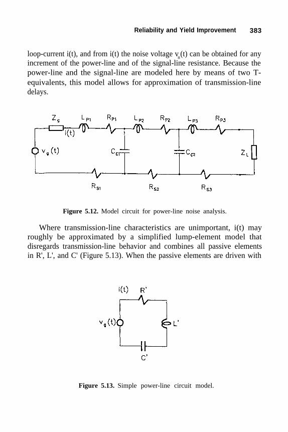
Reliability and Yield Improvement 383
loop-current i(t), and from i(t) the noise voltage vn(t) can be obtained for anyincrement of the power-line and of the signal-line resistance. Because thepower-line and the signal-line are modeled here by means of two T-equivalents, this model allows for approximation of transmission-linedelays.
Figure 5.12. Model circuit for power-line noise analysis.
Where transmission-line characteristics are unimportant, i(t) mayroughly be approximated by a simplified lump-element model thatdisregards transmission-line behavior and combines all passive elementsin R', L', and C' (Figure 5.13). When the passive elements are driven with
Figure 5.13. Simple power-line circuit model.

384 CMOS Memory Circuits
a voltage step vg (t) = Vg 1(t), the Laplace transformed of the loop currentI(p) may be expressed as
The reverse-transformed of I(p) to the time domain i(t) yields that
Here,
Depending on the magnitude relationship of 1/π and ω0 current i(t) can beeither a nonperiodical or a periodical phenomenon (Figure 5.14).
Figure 5.14. Periodical and nonperiodical power-line noise signals.

Reliability and Yield Improvement 385
For both cases the maximum loop-current may be approximated by
where
and
Knowing , the maximum voltage drop across any increment of the powerwire can be estimated, and, in turn, the changes in operating and noisemargins and precharge and logic levels can be calculated (Section 3.1.3).For more accurate computations of the levels, and shapes of noise signals,computer aid with models comprising transmission line losses andreflections should be used (Section 4.1).
The equations of i(t) and indicate that power-line noises may bedecreased to acceptable levels by applying highly conductive materials andby limiting line lengths in the arrays. An increase in line width isconstrained not only by packing density decrease, but also by the increase of
time constant τ, despite that L' = f(LP) decreases with increasing line width.
Nonetheless, an increased L may be compensated by increasedP
C' = f(C ) because the maximum crosstalk current i is inversely proportionalc
with ω0. In some CMOS memories, a large Cc between V and VDD SS isimplemented as a chip-external capacitor on the printed board or in thepackage of the integrated circuit.
5.2.5 Thermal Noise
Thermal noises may set the theoretical limit to the minimum signalamplitude that can be sensed, but crosstalk and power-line noises are the

386 CMOS Memory Circuits
dominating noise events in CMOS memories even at very small featuresizes. Thermal noises, nevertheless, add to the effects of the other noises indegrading reliability parameters, e.g., soft error rates SERs and, therefore,the ratio of the data-signal amplitudes to thermal noise-signal amplitudes ρSN
should be large.
Among the variety of memory types, the expected thermal noisecontribution to the SERs is the highest in dynamic memories, because theystore the data on capacitors. On a capacitor C the average of the thermal-noise induced voltage fluctuations vC may be determined by using thethermal noise voltage v across a resistor R in a simple RC circuit (FigureR
5.15). In the depicted RC circuit,
Figure 5.15. Modeling thermal-noise effects on a capacitance.
K is the Boltzmann constant, and T is the temperature in Kelvin grades.The analysis results that the average thermal-noise induced voltage

Reliability and Yield Improvement 387
is independent of R. Applying vC to a dynamic differential sense circuitthat uses a crosscoupled differential amplifier (Figure 5.16), and assumingthat all transistors in the amplifier operate in their saturation regions andall passive elements are linear; the signal-noise ratio ρSN can be approxi-mated [57] as
Figure 5.16. Differential sense circuit used in approximation ofsignal-noise ratio. (Derived from [57].)
The equation for ρ SN leads to the conclusion that higher prechargevoltage V and supply voltage VPR DD , large data storage capacitance CS anddummy cell capacitance C , small bitline capacitance C , high transistorD B
gain-factor β, long sense time t , small storage charge decay η, lowsen
transistor noise cofficient γ and low temperature T, improve the data-to-thermal-noise ratio ρSN. Circuit coefficient KT and its constituents, the gate-source voltage VGS and the threshold voltage VT of the crosscoupled

388 CMOS Memory Circuits
transistors MN1 and MN2, are established by the design of the sense circuitand can be considered constants in ρSN calculations. Improving ρSN, byadjusting the component parameters of ρ , decreases also the sense circuits'SN
sensitivity to crosstalk signals, power line noises and to the effects of atomicparticle impacts. Thus, the effects of thermal noises on memory operationsdecrease with all facets of the general reliability improvements.
5.3 CHARGED ATOMIC PARTICLE IMPACTS
5.3.1 Effects of Charged Atomic Particle Impacts
Impacts of charged atomic particles may result in randomly located andrandomly timed anomalies in the memory operation. These anomalies areobserved in both terrestrial [58] and space [59] environments, and attributedto ionization in the semiconductor material by alpha particles radiated fromthe memory's own packaging and by a variety of ions, protons and electronsever present in cosmic-rays and cosmic events. Alpha particles are emittedby the thorium and uranium contamination of the chip-package and lead-frame materials. Other materials used in the processing may also radiate atrace amount of ionizing particles. In cosmic environments, the impact ofheavy ions, including the members of the iron group with atomic numbers ofZ>22, of the aluminum group with Z=10-21, and of the carbon group withZ=3-9, as well as the alpha particles (He+ ) and protons, cause mostfrequently errors in memory circuits.
On the Earth, the alpha and other radiations from memory-chippackaging and lead frame may induce soft-errors by upsetting the logic stateof memory cells and sense amplifiers and, in a much lower probability, byupsetting the functions of the peripheral logic circuits. Nevertheless, in theeffected circuits these radiations do not cause permanent damage.
In cosmic environments structural damages and, thereby, hard-errorsmay also appear as results of impacts of very high-energy particles, inaddition to frequent soft-error occurrences. In the near-Earth atmosphere,e.g., in high-flying airplanes and missiles, the incident ionized particles areof low atomic numbers and, usually, do not have sufficient energy todirectly induce errors. However, high-energy charged atomic particles maybe generated indirectly by nuclear reactions initiated by the incidents of

Reliability and Yield Improvement 389
medium-weight alpha particles, protons and neutrons in the semiconductorcrystals and in the oxide materials, and these generated particles mayprovoke operation errors. In semiconductor memories, which have tooperate within the belts of ionizing particles trapped by the Earth’s magneticfield, e.g., in satellites orbiting around the Earth, errors occur most often dueto MeV-protons. In the regions outside of the effective magnetic field of theEarth, i.e., in the cosmic space, the impacts of heavy cosmic ions are theprincipal causes of errors. Most of the error-causing particles have very highaverage energy ranking 10-1000 MeV, and appear in cosmic rays and solarwinds. Protective shielding against cosmic events effects are ineffective,because the reduction in incident ion-energy, so obtained, is usuallyinsufficient to appreciably effect the total charge amount induced by thecosmic particle impact.
The ultimate effect of the impact of a charged atomic particle is thecreation of free electron-hole pairs along the path a particle travels throughthe material and around the centers of nuclear bursts initiated by an incidentparticle in the semiconductor material. In accordance with the generallyaccepted models for particle impacts [510], those electrons and holes whichare raised to the conduction band within the depletion regions and within thegate insulators are separated by the rather high electric field induced by thepotentials of the drains, sources and gates of the transistors and by thesupply voltage and ground nodes. Electrons are swept to the positivepotential, and holes are swept to the negative potential regions. Electronsand holes generated outside the depletion region diffuse through the bulksilicon, and those reaching the boundaries of the depletion region are sweptinto the storage area. At the data storage nodes, the sense amplifier inputsand various other nodes, the prompt appearance of free electrons and holesgenerate spurious currents which may upset the stored or the processed data.
The upsets are randomly located in the memory and randomly timedduring memory operations. These types of anomalies in memory operationsare called single-event-upsets (SEUs) or single-event phenomena (SEP). AnSEU rate of a memory is the number of error events caused by SEU per timeunit per memory. Since in a well designed CMOS memory, most of the soft-errors are results of particle impacts, the number of soft-errors per time unitper circuit the soft-error-rate (SER), and the number failures per one billion

390 CMOS Memory Circuits
device-hours per memory chip, i.e., the failures-in-time (FIT) are also used,somewhat imprecisely, to indirectly indicate SEU rates. Particle impactinduced SEUs have the highest probability to cause the shortest mean-time-between-errors (MTBE) and mean-time-between-failures (MTBF). ThusSEU or SEP rates, SERs and FITs are important indicators of CMOSmemory reliabilities.
5.3.2 Error Rate Estimate
For characterization of a memory's susceptibility to atomic particleimpacts, mostly the SER is used. The SER is usually provided by themanufacturer as results of accelerated tests. During development and designof a memory, however, test data are scarce or unavailable, therefore the SERshould be analytically approximated.
To a memory's SER, the following approach provides an estimate withina factor of two. In this estimate, the circuit-technical base is the introductionof equivalent critical charge QC. Here, the critical charge determines theminimum quantity of charge which is able to alter the logic state of amemory cell, and the equivalent critical charge is defined as the charge-quantity that degrades an operation margin to zero in a sense circuit.
The equivalent critical charge QC can directly be determined, by usingthe node capacitance Cn , the width of the particular operation margin V ,m
and the time constant τn=Cn RL of the data leakage in normal operation;
In the expression of τn , the equivalent resistance RL can be determinedby the node voltage and the leakage current from the node. The time integralof the current pulse i(t) that induced by the impact of a charged particle(Figure 5.17)
provides connection between the critical charge and the current pulse.

Reliability and Yield Improvement 391
Figure 5.17. Current pulse generated by an atomic particle impact.
To change a datum in a static memory cell, in addition to the criticalamount of charge QC a minimum peak current i P also has to be reached(Sections 2.4 and 2.5). With current iP an equivalent critical charge Q Cs mayapproximately be calculated as
where td is the impulse duration form 0.1ipr to 0.1ipf , and i pr and i pf are therise and fall edges of the impulse.
To generate QC the incident particle must deposit a sufficient amount ofenergy in the material. The deposited energy is a function of the energy ofthe incident particle E, the stopping power dE/dx, and of the length of theionization track x in the material. The track length x depends on the incidentangle α, atomic number Z, mass M, and initial energy E0 of the incidentparticle.

392 CMOS Memory Circuits
An exact calculation of the various energy depositions for the variouspossible track lengths is a complicated problem and requires extensive useof computers. Moreover, the computations with the incident uncertaintiesdisallow an explicit expression of individual particle energy deposition. Firstorder approach to energy deposition [511], however, may be obtained bytaking an average track length through the sensitive region.Approximating the sensitive region by a parallel-piped of dimensions 1, w,and h, the average track length can be expressed as the ratio of the volumeVn =1 x w x h and the average projected area
Along a track length S the energy deposited in the sensitive volume E is
and E should exceed a minimum energy to be able to perturb dataDeposited energy E can be related to the equivalent critical charge Q C, atassuming an ionization rate in silicon vi =3.6 V/carrier pair, electron chargeq= 1.60203 x 10⁻¹³ , electron mass energy equivalent ρ
e= 5.109 x 10 - l MeV,
and a charge collection efficiency fn,by the equation
length is
Combining the equations of Q C with the expression of E yields that theminimum stopping power d /dx required for minimum deposited energyE to generate an equivalent critical charge Q C along an average track

Reliability and Yield Improvement 393
For particles which meet the energy and stopping-power requirementsthe omnidirectional flux φE [number of incident particles/cm²day] may beobtained from φE = f(Qc,S) functions (Figure 5.19). The product of flux φE
and average projected area Ap of the sensitive region approximates the SER.For a memory cell SERcell is
Figure 5.18. Stopping-power versus energy for various atomic particles.
Thus, E and dE/dx restrict the incident particles, which may cause errors,to certain types and energy ranges. Both the particle types and energyranges can be determined from experimental or calculated stopping powerversus energy curves [512] (Figure 5.18).

394 CMOS Memory Circuits
Figure 5.19. Omnidirectional flux versus critical chargeat constant lengths. (Source [511].)
The SER of a memory array SERarray
is the SERcell
multiplied by thenumber of memory cells on the chip N
This approach to SER chip neglects the soft-errors which may occur onthe sense amplifiers and other precharged circuits. Although sense amplifiersoften have the most error-prone circuit nodes (Figure 5.20), the probabilityof read and write errors due to incorrect sensing is by factor of 104–108 lessthan the error-probability of data upset in the memory cells and cell arrays.

Reliability and Yield Improvement 395
Figure 5.20. Error-prone nodes in a sense amplifier circuit.
This is because in a memory chip sense amplifiers occupy very littlesilicon area in comparison to the memory cell arrays, and because the stateof a sense amplifier can be changed by particle impacts only in a smallfraction of the read or write cycle times. Nevertheless, a particle hit on asense amplifier may cause burst errors, and therefore designs for extremeenvironments may have to consider the soft error rate of the senseamplifiers SERSA and
where M is the number of the sense amplifiers per chip, and A'P is the totalaverage projected sensitive area in a single sense amplifier circuit.
Decoder circuits may also be susceptible to atomic particle impacts,especially in designs which allow floating nodes. A particle hit on thefloating nodes, or on nodes coupled to others only by high impedances, mayresult in placing correct data into incorrect addresses. Thus, incorrect

396 CMOS Memory Circuits
addressing by the rate of soft-errors in the decoder SERDEC should also beregarded in the chip total SER
Here, K is the number of equivalent decoder subcircuits per chip and A P"is the average projected sensitive area per subcircuit.
Other circuits, in a memory chip, may also be susceptible to charged-particle impacts, but experiments proved that their contribution to the soft-error rate of memory chip SER chip is insignificant in most of the designs.Thus, the SER chip may be approximated as
In terrestrial environments, experimental SER data on CMOS memoriesnormally yield a simple step-like function in the diagram of the exper-imental particle-sensitive cross section σ versus linear energy transfer LET(Figure 5.21).
Figure 5.21. Particle-sensitive cross section as a functionof linear energy transfer. (After [513].)

Reliability and Yield Improvement 397
LET [eV/mg cm²] is the linearized equivalent of the stopping powerdE/dx, and σ is the experimental counterpart of the theoretical AP, and at agiven LET
where Rr is rationalization factN, K. The simple σ = f(LET) curve is usually reduced to a two-point dataset that includes the saturated cross section σS and the threshold LET Lt. L t
may be determined either by linear extrapolation of the σ curve or byprojection of 0.1 σS to the LET axis. For ions depositing charge aboveLET = L
t the geometric surface area of the sensitive volume σ increases
rapidly to σS. At σS the collected charge is large enough for every incidentparticle that strikes the sensitive volume to cause an upset, and σS remainsapproximately constant with further increasing LETs. Experimental σS andLt provides acceptable SER accuracy in estimation of terrestrial packageradiation effects, but for complex circuits operating in cosmicenvironments σ =f(LET) often differs from a step function, and thespectrum of particles, their energy and fluxes vary with the location andtime of the orbiting or travelling space object [513].
or for convenient analysis of e.g., Rr = M,
For both space and terrestrial applications increased accuracy in SERprediction can be obtained by the use of another parameter, the errorprobability per particle incidence ε [514]
where D(Q) is the probability that the generated charge Q appears in anerror causing zone ∆Q

398 CMOS Memory Circuits
Here, E is the kinetic energy, α and β are the incident angles, XP and Y P
are the incident position coordinates and F is a normalized distributionfunction.
5.3.3 Error Rate Reduction
The first order approach to SER calculations (Section 5.3.2) demonstratethe desirability for large equivalent initial charge, large data-hold current,short track lengths through the sensitive volume and small collectionefficiency as means of SER reduction. Both the critical charge and thesensitive track lengths decrease with the evolution of the CMOStechnology. Nevertheless, the SER increase by reduced critical charges ismore significant than the SER decrease by shorter track length.
Traditionally the best SER characteristics are provided by full-complementary 6T static memory cells due to their high data-hold currentsfor both log.1 and log.0. In fact, 6T static memory cells with added resistiveand capacitive RC elements (Figure 5.22) for QC increase, are the prevailingchoices to memories operating in space, military and other extremeenvironments [515], in spite of these cells' rather large size. Since the size of6T cells can be made the same as that of the 4T2R cells by placingpolysilicon thin-film transistors on the top of the traditional transistors(Section 2.4.4) high packing density can be combined with very low SER,very low power dissipation and high operational speed.
To limit SER, dynamic memory designs enlarge storage capacitors byusing three-dimensional (3D) structures and thin insulators with highdielectric constants in dynamic 1T1C memory cells (Section 2.2.4). In staticmemory technology, the quest for low standby dissipation and high packingdensity resulted in 4T2R memory cells with extremely high load resistances,low hold currents and small node capacitances, which increased the SER 's ofthe CMOS memories. SER can be improved in 4T2R memory cells by theincrease of the current drive capability of the constituent transistors and ofthe storage node capacitances (Section 6.2.4). Device current and nodecapacitance enlargements are limited, nevertheless, by the practicallydeliverable write currents and by the projected size of the memory cell.

Reliability and Yield Improvement 399
Figure 5.22. Six-transistor static state-retention memory cells.
In CMOS memories SER decrease can also be obtained by using currentsense amplifiers because of their low input impedances. In voltage senseamplifiers, a reduction in input impedance results also in receding particle-generated spurious signals [516] (Figure 5.23) and in smaller SERs for thecircuit. Reduction in SERs can be obtained, furthermore, by decreased

400 CMOS Memory Circuits
number and, ultimately, by elimination of sense amplifier circuits, e.g., byusing orthogonal shuffle and shift register type of memory arrays.
Figure 5.23. Particle-generated spurious signals on a sense amplifierinput node at different input-impedances.
In commercially applied memories, the large bit-capacity per chip andcost-effectiveness are the primary concerns and, therefore, most of thecommercial memories use the smallest possible dynamic 1T1C and static4T2R memory cells. To improve SER in commercial memories, the storagecapacitances and hold currents have been increased, and the collection effi-ciencies have been decreased, by process technological approaches, e.g., bythree-dimensional structures, doping profile adjustments in the channelareas, epitaxial layers, etc. Because these process technology improvementshave been developed simultaneously with feature-size downscaling thefailure-in-time (FIT) per bit for terrestrial alpha-particle impacts has beenimproved with increasing memory bit-capacities per chip (Figure 5.24).With increasing FIT per bit the soft-error-rate SER lessens. Lessening SERsindicate that terrestrially applied memories may not need any specialcircuit techniques to reduce alpha particle sensitivity. Nevertheless, theneed for special circuit techniques within the memory, or in the system

Reliability and Yield Improvement 401
outside of the memory, can be determined only after SERs have beenthoroughly analyzed on the specific memory design.
Figure 5.24. Failure-in-time versus DRAM bit-capacity.
For CMOS-bulk memories the epitaxial and other buried layers may bedesigned so that they divert the free charges induced by incident atomicparticles from the data-holding nodes and, thereby, they decrease considera-bly the charge collection efficiency of the memory circuit nodes.
More improvement in memory SERs can be achieved by the applicationof CMOS-silicon-on-insulator CMOS-SOI and silicon-on-sapphire CMOS-SOS fabrication technology. CMOS-SOI and CMOS-SOS structures pro-vide short possible track-lengths for an incident particle because they applyvery thin silicon films and because the sizes of the transistor islands in thememory cells are small (Section 6.3).
In large bit-capacity memories where the memory cell size minimizationis a primary concern, and in memories in which neither circuit nor

402 CMOS Memory Circuits
processing approaches can satisfy environmental requirements; theimplementation of error detecting and correcting codes (Section 5.7) and,eventually, of fault-repair (Section 5.6) may be justified. Generally, theimplementation of the encoding and decoding of error control codes, theredundant code bits, and the redundant elements for fault-repair, requireadditional circuits and, in turn, compromises in memory chip size,operational speed and power dissipation. Nonetheless, the improvement inmemory reliability, achievable this way, allows to produce memory chipswith bit-capacities, environmental tolerances and yields which are difficultor impossible to attain by other approaches.
5.4 YIELD AND REDUNDANCY
5.4.1 Memory Yield
Memory yield is expressed by the percentage of fully functional memorychips from all of the fabricated memory chips or, alternatively, by the ratiobetween the fully functional memory chips and all fabricated memory chips.Fully functional memory chip means that each and all memory cell andmemory circuit perfectly performs each and all designed functions,i.e., access, write, storage, read, input, output and other operations, under theplanned conditions. The percentage of fully operational memory chipsobtained from all the chips on all the wafers is indicated by the wafer yield,and the yield gained after assembly and packaging is the manufacturingyield.
Memory fabrication yield is limited [517] largely by random photodefects, random oxide pinholes, random leakage defects, gross processingand assembly faults, specific processing faults, misalignments, gross photodefects and other faults and defects (Figure 5.25). The defects and faultsresult predominantly in random single bit errors and much less frequently,in burst, cluster and double bit errors, and also in totally dysfunctional
The need for memory yield improvement has been instrumental in thedevelopment of yield models for all types of semiconductor digitalintegrated circuits [518]. Yield models approximate the probability that theyield is Y. Y is a function of chip size A, defect density D, wafer size AW, lot
memories.

Reliability and Yield Improvement 403
Figure 5.25. Distribution of defect types after fabrication.
size N , number of chips on a wafer M, intrawafer fault-clustering factor α ,L 1
interwafer fault-clustering factor α , defect size S, geometrical and other2

404 CMOS Memory Circuits
variables, and a plethora of sophisticated computer programs have beendeveloped and used for yield approximations.
Simple approximations to Y assume that the yield is determined by thecritical area in which point-defects cause functional errors A, and by themean density of point-defects D if the defects were evenly distributed on thedefect sensitive surface. Further assumptions, in simple models, include thatthe defect distributions for Y obey either Maxwell-Boltzmann [519], orPoisson [520], or Bose-Einstein [521] statistics. Rudimentary use ofMaxwell-Boltzmann and Poisson statistics result too pessimisticexpectations, while Bose-Einstein statistics give too optimistic yieldestimates. At high yields all models provide good approximations [522], butthe usual choice of convenience is the Poisson model. Yield calculationswith Poisson model do not require established fabrication data, andcomputations with Poisson statistics is uncomplicated.
A fabrication yield-loss is usually due to a number of different defecttypes rather than to one dominant cause. If for a defect type i the critical areais A , then for a multiplicity of defect types thei and the defect density is Di
assumption of Poisson distribution results a yield
while the Bose-Einstein statistic gives
Individual defect types, nevertheless, tend to cluster into higher andlower defect density area. Dividing the wafer area S to Si regions, so thatS = ΣS is the area of the i-th region over which the defect density isi, and Si
reasonably uniform; a good yield estimate for a single wafer may beobtained by [523]

Reliability and Yield Improvement 405
Somewhat more sophisticated models attempt to consider clustering byincluding probability density functions P(D) or PDF [524]
For P(D) a number functions are introduced and good yieldapproximations are obtained by the use of triangle distribution
gamma functions [525]
and Erlang distribution [526]
where Do is the average defect density, σ is the standard deviation and K isthe number of processing steps.
Semiconductor processing may cause defects which greatly vary in theirsizes. Defect size variations may be considered by the applications ofprobability density functions PDFs [527]. From the plethora of PDFstatistical distribution functions, so far, the Rayleigh distribution

406 CMOS Memory Circuits
brought the most acceptable results in modeling single source defects.Here, x is the distance along the wafer diameter, and γ is the defectdistribution parameter.
Processing experience indicated that both on-wafer and wafer-to-waferdefect density distributions differ from each other, and most of the chips onthe wafer edges are unusable. Assuming within a wafer and among wafersthe defect density distribution can be modeled by Poisson and gammadistributions respectively, then for i types of defects the yield [528] is
where Yo is the yield after gross failures, λ is the expected number ofi
defects, and αi is the clustering coefficient. In large chips the distinction ofintrawafer clustering coefficient α1 from interwafer clustering coefficientα2 is of increased importance. With the number of on-wafer fault-causingdefects λ , fault distribution function for λw w -s wafer-to-wafer variationsg ), fault density q, fault distribution on a single wafer P(w(λw λw,q) and totalnumber of circuits N; a formula [529] which reasonably estimatessemiconductor memory yield Y may be obtained as
Here, by P and gw are Poisson and gamma distributions, but other distributionfunctions may also provide results which approach the experientially acquiredyield figures.
5.4.2 Yield Improvement by Redundancy Applications
Memory yields can be improved, in addition to stringent fabricationcontrol and statistical worst-case design, by implementation of redundancy.For yield increase redundancy is implemented by on-chip spare elementsincluding spare bits, rows, columns and blocks of memory cells, duplicationand triplication of sense, and peripheral circuits, or by repetitions of entirememory circuits. Furthermore, on-chip circuits implementing error detector

Reliability and Yield Improvement 407
and corrector codes are also frequently applied in CMOS memories for yieldimprovements, particularly in large read-only and nonvolatile memories.Redundancy in memories increases access and cycle times, powerdissipation chip area, and require modifications in the design. Because of thesubstantial design tradeoffs, careful analysis should precede the decisionwhether redundancy should be used, and if it is used, how much redundancywould approximate the maximum achievable yield improvement.
Memory yield improvement by on-chip redundancy applications isjustified mostly by requirements for (1) reducing cost-per-bits in largecapacity memories, (2) increasing memory bit capacities at immatureprocessing, and (3) providing fully functional parts in very low volumememory production. Cost-per-bit of CMOS memories, with or withoutredundancy, as of other integrated circuits, can also be decreased byreduction of chip sizes. Thus, CMOS memory chips designed withoutredundancy application may result considerably lower cost-per-bit thanmemory chips designed with redundancy do. The use of redundancy mayalso allow for obtaining fully functional memories fabricated with immatureprocessing technologies when the amount of processing defects would causenear zero manufacturing yield. Moreover, with redundancy some yield maybe acquired in such a few processing lots and runs, in which processingparameter variations do not follow the distribution statistics that the memorydesigner assumed. For correctly designed memories, nonetheless, which arefabricated in large volumes, the very redundancy, which is rendered toimprove yield, may become a yield limiting factor as the fabricationtechnology matures with the time of production (Figure 5.26). To improveyield after the processing matured, the design should provide the option ofremoval of the inept redundant elements from the memory.
Memory yield improvement by redundancy applications is limited bythe amount of redundant elements used on a single chip. On-chipredundancy increases the chip size, and the expansion of the chip size tendsto reduce yield. Yield improvement by redundancy implementations may bedesigned (1) by optimizing the number of on-chip redundant elements toobtain the highest achievable yield, and (2) by using a given number ofredundant elements and compute their effects on the yield. In CMOSmemory yield improvements, the amount of redundancy for the memory cell

408 CMOS Memory Circuits
Figure 5.26. Yield increase as a function of fabrication maturity.
arrays are usually optimized, while for the duplication or triplication ofelements to peripheral circuits, or functional entities, the yield is designedto be higher than that of the arrays. In memory circuit designs, the yieldoptimization and yield computation rely on both appropriate statisticalmodels and experimental data.
A model's exactitude in estimating memory yield depends greatly on theparameters of the applied fabrication technology, fabrication facility andcircuit design, and what is more, the validity of various models are widelydebated and challenged. Inadequacy or misuse of models in yield prediction

Reliability and Yield Improvement 409
may lead to financial disasters. For yield optimization, however, not theyield itself but the amount of spare memory cells that maximizes memoryyield, i.e., the optimum number of redundant elements, is the most importantparameter. To estimate the optimum number of redundant elements for aspecific memory design, the evaluation of the effective yield Y versus theeff
number of redundant elements NR at constant defect densities and at givennumbers of critical layers (Figure 5.27) may favorably be applied. At acertain defect density, the effective yield is the ratio between the number of
Figure 5.27. Effective yield versus number of redundant elementsfor a DRAM with 1-Mbit redundant elements.
chips on a wafer with redundancy and the prospective number of chips onthe same wafer without redundancy multiplied with the percentagefabrication yield, at a specified number of critical layers. In CMOSmemory technology critical is the layer (the mask and the accompaniedprocessing steps) in that a small, but finite size, defect can impair thefunction of a storage cell. The same defect size, that impairs memory cells,can not necessarily make other memory circuits dysfunctional, because the

410 CMOS Memory Circuits
packing density of peripheral circuits is usually much less than that ofmemory cell designs. A memory cell as well as complete rows, columns,blocks or arrays of memory cells and any other subcircuits, may bereplaced by their on-chip copies which are designated, here, as redundantelements. Above a certain number of redundant elements the effectiveyields curve optimums. These optimums are rather flat and appearsapproximately at the same number of redundant elements when computedwith a variety of different models. Computation results for effective yieldsand optimum number of redundant elements indicate that for lower defectdensities smaller number of redundant element provide optimum yield,and the effective yield increases with lower defect densities.
Yield increase of large memory chips, e.g., ultra high scale integratedULSI and wafer scale integrated WSI memories, may require duplication2X, or triplication 3X of peripheral circuits, whole memory arrays orcomplete memories. Since in 2X and 3X redundant memory circuits theamount of redundancy is given, the anticipated fabrication yield of theredundant memory YR is the parameter to be obtained. For convenientcomputations, the yield with redundancy Y may be viewed as a product ofR
three terms [529] gross failure limited yield Yo , random defect limited yieldwithout redundancy Y, and random defect limited yield with redundancy Yr
YR = Yo YYr
Yo is usually obtained from fabrication experience, while Y can either beextracted from fabrication experience, or be approximated by one of thepreviously discussed analytical yield models. For calculation of Yr , yieldmodels are often used, because experimental results for Y can be scarce atr
the onsets of the designs. Yr may be approached by dividing the chips intoβ number of equal size domains, each domain into two identical prime andunprime elements, and an element into n number of circuits. While thetotal number of wired up circuits required to function is N = nβ, the totalnumber of circuits per chip in 2X redundancy configuration is 2N =N1 .Assuming any single fault impairs only one element, the yield Yr may beexpressed as

Reliability and Yield Improvement 411
where K is the domain identification number and q is the density of thelocal fault-causing defects. If the qK-s are Poisson distributed, Yr may wellbe approximated by
where λ wo is the expected number of faults in N circuits.
The approach to Yr of duplicate redundancy may be extended to higherorders of redundancy when one element out of R elements should befunctional, e.g., in the special case of Poisson statistics
R = 3 for simple triplicate redundancy in that a minimum one out of threeidentical elements should operate. If two out of three identical elementsmust work, e.g., in a majority decision configuration where the voter isfunctional, Yr becomes
The expressions of Yr illustrations the yields' increasing sensitivity to theexpected number of faults λwo with increasing amount of redundancy.
In any real situations, λwo tend to cluster on a wafer which may beconsidered by an interwafer clustering parameter α1, and both λwo and α 1
vary wafer-to-wafer which may be regarded by an intrawafer clusteringparameter α2 . In general, the yield with redundancy YR is a complex triple orquad integral expression where
Numerical evaluations of YR, for the case when both P (Q) and gw(λw) aregamma distributions, indicated that yield reduction from intrawafervariations may be compensated for by interwafer variations, and that the

412 CMOS Memory Circuits
yield is more sensitive to interwafer clustering than to intrawaferclustering in large chips and wafers (Figure 5.28).
Figure 5.28. Yield sensitivity to defect clustering. (After [529].)
On-chip redundancy that improves yield, does not necessarily improvereliability, although the substitution of marginally operating elements bygood ones, increases both reliability and yield. For both yield and reliabilityimprovements the application of circuit redundancy is essentially the same,and can be discussed without discrimination for the intended use.
5.5 FAULT-TOLERANCE IN MEMORY DESIGNS
5.5.1 Faults, Failures, Errors and Fault-Tolerance
In memory technology, as in digital circuit technology the terms fault,failure, and error have distinguished meanings [530].
A fault is an anomalous physical condition. Causes of anomalies includedesign deficiencies, manufacturing problems, damages, fatigues, deterior-

Reliability and Yield Improvement 413
ations, extreme ambient temperatures, ionizing radiations, humidity,electromagnetic interference, internal and external noises, misuse, etc.Usually, memory faults are classified by their duration, location, extent andnature (Table 5.2).
Fault
Duration Location Extent Nature
TransientIntermittentPermanent
Memory CellBitline
WordlineSense Amplifier
Read CircuitWrite Circuit
Address CircuitControl CircuitClock Circuit
Supply NetworkInputOutput
SingleMultiple
RowColumnArray
DecoderPeripheral
Global
Stuck-atTiming
Floating
Table 5.2. Fault classification.
A failure is the inability of a memory cell, circuit element, circuit or anentire memory to perform its designed function, which inability is caused bya fault.
An error is a manifestation of a fault in a memory, in that logical state ofa memory cell or a peripheral circuit element different from its intendedstate. Different errors may be categorized by occurrence, direction, pattern,location and orientation (Table 5.3), and all errors can be hard or soft. Ahard-error is a result of permanent damage, which may appear either throughan abrupt or through a drift failure mode, in a circuit element. A soft errordoes not persist in the effected circuit after the fault-causing phenomenondisappears, and at reuse the circuit operates as designed without any repairor correction in the memory chip.

414 CMOS Memory Circuits
Occurrence
RandomSystematicClustering
Pattern
SingleDoubleQuadBurst
MultipleBurst
Direction
BidirectionalUnidirectional
Error
Location
Memory cell Row
ColumnSense –
AmplifierLogic –
ElementInput
OutputGlobal
Orientation
SymmetricalBiased
Table 5.3. Error categories.
Those memories which feature on-chip fault repair or error-correctioncircuits are referred, though somewhat inaccurately, as fault-tolerant memo-ries. Fault-tolerance in memories is applied to improve reliability, or yield,or both. Fault tolerance is crucial for reliable operation in space, nuclear,military and other extreme environments, and important to increase yielduntil the fabrication technology matures. Nonetheless, mature memoryproducts operating in standard environments need rarely on-chip fault-repairor error correction to enhance fault-tolerance.
Fault-tolerance within a memory chip is achieved by redundancy inmemory cells, arrays, peripheral circuit-elements and in the redundancycontrol circuits. The implementation of redundancy may profoundly influ-ence the layout area, speed and power performance and, therefore, must beplanned for at the outset of a memory design.
The plan's objective is to establish whether and how much improve-ments in reliability and yield are required and what techniques are to be usedto implement the required improvements. To determine these requirementsthe circuit design needs to know:
(1) What types and amounts of faults and errors appear and areeconomical to repair and correct,

Reliability and Yield Improvement 415
(2) What the optimum strategies are to tolerate the faults and errorsto be repaired and corrected.
Analyses of faults and errors, which may occur in a particular memory,indicate the reliability and yield parameters of the memory designed withoutparticular features for fault-tolerance. A comparison of the actual reliabilityand yield parameters to the desired ones show whether any or how muchimprovement is necessary, while the strategy of improvement depends onthe types and amounts of dominating faults and errors.
5.5.2 Faults and Errors to Repair and Correct
For determination of types and amounts of those faults and errors whichare necessary and economical to repair or correct for achieving a desired
Error Sources Hard-Errors Soft-Errors
Fabrication and Design
Hot carrier emission XElectromigration XSurface charge spreading X XIonic contamination XSpurious currents X XTime dependent breakdown X
Environmental
Package alpha radiation XStatic charge and discharge XElectromechanical corrosion XElectrochemical corrosion XElectromagnetic interference X XTemperature X XCosmic particle impacts X XRadiation total dose X XTransient Radiation X XMechanical shock X XElectrical shock X
Table 5.4. Hard- and soft-errors influencing reliability.

416 CMOS Memory Circuits
reliability or yield, analyses of the failure modes faults, and errors areneeded in each individual design variation of the memory circuits. Thespecific goal of the circuit failure mode analysis is to establish theperformance requirements for fault-repair and error correction. Theperformance requirements of reliability improvements may greatly differfrom those of yield increase. Namely, reliability is influenced by bothhard- and soft-errors arising from faults in memory fabrication, design andenvironmental sources (Table 5.4), while yield is effected by hard errorsonly, which may be caused by fabrication and design issues (Table 5.5).
Fabrication
CleannessMaterialsMaskingOxidesParameter spreadComplexityControlTemperatureMechanical shock
Design
Feature sizeChip sizePacking densityCell typeLayoutParameter variation toleranceFault-tolerancePattern sensitivity
Table 5.5. Fabrication and design issues effecting yield.
In each of the memory circuits, fabrication, design and environmentaleffects can cause faults through circuit-specific failure mechanisms, and thespecific faults are manifested in either symmetrical or unidirectional errortypes. Circuit faults appear in the data outputs of the memory, mostfrequently, as discrepancy between write-and-read data and as data stuck atlog.0 or log.1 (Table 5.6). A write-read data discrepancy may be caused by afailure either in the addressed memory cell, or in the sense circuit, or in theaddressing circuit. Stuck-at faults may occur in any of the circuits, andthey may result from three major categories of failure modes in transistordevices and interconnects (1) parameter degradations, (2) short circuits,and (3) open circuits [531]. Parameter degradations and open-circuit faultsmay result in intermittent levels between log.0 and log.1, but eventuallythese intermittent levels are amplified to standard log.0 and log.1 levels,

Reliability and Yield Improvement 417
while short- and many open-circuit faults cause immediate sticking oflogic operations at standard logic levels.
Faulty Circuits
Data Input
Address Input
Word Decoder
Word Line
Storage Cell
Bit Line
Bit Decoder
Sense Amplifier
Read Line
Read Amplifier
Write Amplifier
Data Output
Data Output
Stuck at log.0 or log.1
Discrepancy between write and read data
Discrepancy between write and read dataPeriodic appearance of same set of data
Stuck at log.0 or log.1Discrepancy between write and read data
Stuck at log.0 or log.1
Stuck at log.0 or log.1
Discrepancy between write and read dataPeriodic appearance of same set of data
Stuck at log.0 or log.1
Stuck at log.0 or log.1
Stuck at log.0 or log.1
Stuck at log.0 or log.1
Stuck at log.0 or log.1
Table 5.6. Circuit faults and their most frequent effects on the data output.
Data discrepancy and logic level faults may represent a large variety ofphysical failures, but they do not cover all possible failure modes, e.g.,power-supply line short and break, pattern sensitivity, etc. Nevertheless, thecoverage of dominant failure modes is sufficient for establishing what faultsand errors should be tolerated in the memory by on-chip repair and cor-

418 CMOS Memory Circuits
rection. By using spare chips in a system, of course, the memory operationcan be sustained despite the presence of any number and types of faults anderrors.
The frequency of faults and errors depends mostly on the memory circuitand layout design, processing technology, starting material, handling,operating and storage environments. Experience in these issues indicatesthat in CMOS VLSI memories the single random type of errors (Figure5.29a), but in CMOS ULSI and WSI memories, beside the dominatingsingle-random errors, the number of double and quad errors in the memorycell (Figure 5.29b) may also be significant in addition, of course, to othermiscellaneous error types.
In addition to the determination of the most frequent type of faults anderrors, the effects of memory malfunctions on the system operation, has tobe weighed. A system operation may absorb certain low amounts of singlebit errors, but the appearance of a burst error may have catastrophic conse-quences. Burst errors in memories are caused most likely by the malfunctionof a sense amplifier and, with much less probability, by impairment in someperipheral memory circuits.
Generally, a fault tolerant CMOS memory design has to cope, mostlikely, with hard and soft errors which are (1) symmetrical and occurrandomly in single and double bit patterns in memory cell arrays, and(2) unidirectional and occur as bursts in sense amplifiers.
More prominent appearance of double, quad and burst errors, as well assimultaneous impairments of neighbored rows and columns, are anticipatedwith the further evolution of the fabrication technology toward smaller fea-ture sizes, and with applications of CMOS memories in increasingly severeenvironments. Gross errors and global faults impairing entire memory chipsmay be tolerated in system levels by enabling spare chips. Yield increase byuse of spare chips can be considered only in integrated chip systems such asmulti-chip-module (MCM) and WSI memories. The analysis of memoryfailure modes and the experience in fabrication, design and application inspecific environments reveals what classes of errors and faults at whatfrequentness may appear and what is desirable to tolerate. Additionally theimplementation of fault-tolerance requires a strategy that is amenable to the

Reliability and Yield Improvement 419
Figure 5.29. Error-type distributions occurring intwo different CMOS memories.

420 CMOS Memory Circuits
repair or to the correction of the faults and errors determined by thefailure-mode analysis.
5.5.3 Strategies for Fault-Tolerance
The right fault-tolerance strategy is the approach that provides therequired performance in reliability or yield improvement and the optimumimplementation efficiency in area, speed and power. To satisfy the range ofperformance-efficiency requirements in memory designs, a fault-tolerancestrategy may include one or more of the following fundamental techniques:
•
••
••
•••
•••
Repair by reconfiguration separates, bypasses, and replaces thefaulty element by an operating spare one,
Detection indicates error by application of error detection codes,
Correction reconstructs an acceptable code word from an erroneousdata word by application of error detection and correction codes,
Masking corrects errors by simultaneous use of circuit replicas,
Containment prevents the propagation of erroneous data out of afaulty circuit,
Diagnosis identifies the faulty elements,
Inhibition disallows the use of diagnosed faulty elements,
Timing and protocol checks compare internally generated clockimpulses to each other or to replicas,
Repetition of rewrites and rereads detects erroneous data,
Discarding renders erroneous data unusable,
Maintenance purges errors in the memory operation periodically.
From this variety of techniques, fault-tolerant memory designsincorporate on-chip fault-repair, error detection and correction, and in someinstances fault masking, while the other techniques are applied, so far, off-chip on system level. Nevertheless, the on-chip implementation of anyapproaches may be applied to satisfy the anticipated higher standards inreliability and yield for future large bit-capacity memories.

Reliability and Yield Improvement 421
5.6 FAULT REPAIR
5.6.1 Fault Repair Principles in Memories
Fault repair, here, is a reconfiguration of the memory circuit that inhibitsthe use of faulty circuit elements and enables the use of operating spareelements. Circuit elements which are repaired in a memory include rows,columns, blocks (clusters), subarrays and arrays of memory cells. Individualmemory cells are not, and elements or the whole of peripheral logic circuitsare seldom, practical to repair.
The repair procedure consists of three phases: (1) detection and locationof faulty elements, (2) assignment of operating spare elements, and (3) dis-connection of the faulty elements and integration of the assigned spareelements with the memory operation.
The detection and location of faulty elements or errors are providedeither by error control codes, or by an on-chip tester circuit, or by externaltest equipment. On-chip and external tests allocate also the spare elementswhich are operational, and allow to assign the spare elements to the circuitswhich contain the faulty elements. Disconnection and of faulty elements andengagement of spare elements may be implemented externally by laser, fuseand antifuse programming, or by on-chip repair circuit applying electricalfuse, antifuse, EPROM, EEPROM, FRAM, SRAM or other bistableprogrammable circuit elements.
The operation principle of the memory circuit repair (Figure 5.30) isessentially the same in all types of memories; depending on the content ofthe fault-address memory either the main memory or a spare memory circuitis selected, and from or to either one of both memories the data aretransferred from and to the input-output terminals through an eventualcorrector circuit.
The implementation of repair circuits may have the following objectives:
• Improved reliability at minimum or no impact on yield,
• Improved yield at increased or at no change in reliability,

422 CMOS Memory Circuits
Figure 5.30. Fault-repair principle for memory circuits.
••••••
Minimum increase in area,
Minimum or no degradation in speed and power performance,
Reconfiguration transparent to the user,
Replaceability of both main and spare elements,
Unchanged processing technology,
Easy removability of spare elements.
Reliability improvement, by using spare elements, may decrease the yieldbecause the implementation of spare and repair-control circuits increasesthe layout area. Yield, by varying the number of spare elements, may beoptimized, but the use of spare elements for yield improvements mayreduce the reliability, e.g., by the debris of fused links, decreased noisemargins in electrically programmable memory cells, etc. Nonetheless, bothyield and reliability can simultaneously improve at correctly designed and

Reliability and Yield Improvement 423
executed repair when not only faulty but marginally operating elementsare also replaced.
The implementation of the spare elements and repair-control circuits canbe designed so that neither the access time nor the power consumption of thememory increases palpably, and the application of the memory in systemsdoes not need any change in input and output requirements, pin order, andother parameters. A repair method that would require process modificationraises questions not only about product cost increase, but it may causesubstantial changes in the design of the memory and its testing.
5.6.2 Programming Elements
Programming elements either separate or couple memory and sparecircuit elements by creating low- or high-resistances between circuit nodesarbitrarily. Unprogrammed low-resistance wiring elements are used as fuses,while normally high-resistance semiconductor elements are applied asantifuses. Furthermore, both normally high- and normally low-resistancestates can be provided by any type of nonvolatile memory cells, and also byvolatile memory cells using battery backup.
All the different types of programming elements, which are applicable tomemory designs, may be programmed externally or internally, and all thetypes of fuses and antifuses may be programmed by laser or electricallygenerated heat. Memory cells applied as programming elements operateunder the same write and read conditions as in data storage applications,although they may be designed to prefer an initial log.0 or log.1 state beforeprogramming.
For yield improvement the preferred programming method is the lasercut [532] of a polysilicon or metal link, because its implementationrequires small layout area that can be fitted to a row or column pitch,influences negligibly the speed and power characteristics of the memory,and provides a large resistance change from the unprogrammed (0.1-10Ω) to the programmed (25-250MΩ ) resistance. The layout area of theprogramming link is determined by the effective diameter of the laser spotD and by the inaccuracy of laser beam positioning a (Figure 5.31).

424 CMOS Memory Circuits
Figure 5.31. Diameter, position accuracy and power density distributionof a laser beam to a fusible link design. (Source [532].)
Decreasing memory feature size require improvements in focusing,position accuracy and shorter laser wave lengths. The widely used yttrium-aluminum-garnet YAG lasers provide D=1-3µm, α = ± 0.1-0.3µm andoperate at a wave length of λ = 1.064µm. For the laser beam, in manydesigns, holes are left in the passivation layer to promote the removal ofcontaminants produced by the laser cut. In both polysilicon and metallinks, the laser beam destroys much more than its diameter, because asignificant amount of power under the fuse-threshold is also absorbed bythe link and its surrounding material. Because of this "wicking" the linkshould be the minimum length of LL = D+0.5α + 1w , where 1w is thedestruction length in the link by wicking.

Reliability and Yield Improvement 425
The cut of a polysilicon link results less debris than the cut of a metallink and, therefore, a polysilicon cut results in more reliable separation.Since the separation does not need any other circuit element other than ashort link, the access and cycle times as well as power dissipations areinfluenced only by the interconnect lines necessary to implement the spareelements and in some instances by the load introduced by the spareelements.
For connection and disconnection of spare and faulty elements laserprogrammable antifuse links (Figure 5.32) may also be used. When a laserspot on the link covers the p-n junctions the material melts and provides arather low-ohmic conductance. Both the low and high resistance as well asthe maximum operating voltage and current depends on the characteristicsof the switchable p-n-p, or n-p-n or amorphous device. Antifuses switchnormally high resistances (>l0MΩ) to low resistances (50-300Ω), and intheir high-resistance unprogrammed states the breakdown voltages are inthe range of 3-6V.
Figure 5.32. A laser programmable antifuse link.
The implementation of laser programmable fuses and antifuses is simpleand inexpensive, but the acquisition and maintenance of a fully automaticlaser programmer equipment needs substantial capital investment. For yield

426 CMOS Memory Circuits
enhancement when high capital investment into a laser programmer isimpractical for any reason, or for repairs of memories which operate insystems, i.e., in-situation or in-situ, the fuses or antifuses may be pro-grammed electrically. Nevertheless, the electrical Programming require theapplication of high current, or voltage, or both, that leads to inflated circuitsizes and penalties in speed and power. Even at external application of highvoltage, a part of the on-chip programming circuits has to be able to toleratethe current and voltage stress, and has to contain an interface circuit toseparate the programming elements from the operating elements to maintainreliability standards.
Electrically programmable elements may also be implemented in fuse orantifuse devices. Electrically fusible links have similar layout designs asthose of laser programmable fuses, but the Joule-heat, rather than the lasergenerated heat, evaporates the conductive metal or polysilicon material. Aninsulator material, e.g., Oxygen-Nitrogen-Oxygen [533] or amorphoussilicon [534] is melted between two conductive layers in the mostly appliedelectrically programmable antifuses (Figure 5.33). Electrical antifuses can
Figure 5.33. Electrically programmable antifuse elements. (Source [534].)

Reliability and Yield Improvement 427
provide very high off-resistances (>1G Ω ) and acceptable on-resistances (80-500Ω), and need 3-6mA and 10-20V programming current and voltage.Implementations of electrical programmability may require up to threeadditional mask-layers and extended layout areas.
The layout area of an electrically programmed element may not be assmall as that of a laser programmable element, because its implementationoften needs p+ or n+ doped guard-rings to avoid destruction in thesurrounding circuit elements. Furthermore, electrically programmableelements need at least one extra pad for programming power supply. Theextra pad is not bonded out to package and must be held in an adequatepotential after testing to prevent any inadvertent programming during therest of the fabrication process.
Programming of fuses or antifuses may need slight changes inprocessing to keep open a window in the oxide above the programmableelement. Windows allow for better positioning control and for improved gas,debris and heat escape which are generated by programming.
Fuse and antifuse programming with laser assistance are most suitable toenhance yield of memories which apply dynamic and static (1T1C, 4T2R,6T, etc.) random access memory cells. The reasons for that include the(1) minimum impact of the implementation in circuit area, speed and power,(2) reliability of the programming, (3) reasonability of equipment costs atvery high volume production, (4) unchanged processing technology and(5) easy design for transparency in operations and/or for removability ofspares. Area, speed and power tradeoffs and design difficulties arecompromised more by the application of electrical programming than by theuse of laser programming. Nevertheless, the use of electrically program-mable fuses and antifuses are well justified for reliability improvements andrepairs of memories installed in systems, and to enhance memory yieldwithout substantial investment in laser programmers.
In static and dynamic memories which have battery backup, the appliedmemory cells can also be used for repair programming, especially wherehigh programming speed, cost effectiveness in implementation, and directcompatibility with the controlling logic circuits, are among the requisites.Nonvolatile [535] and battery-backed volatile [536] programming elements

428 CMOS Memory Circuits
may gain applications also in memories, despite needing additionalprocessing steps for implementation of programming elements, where in-situ memory repairs should combine high reliability operation with highspeed performance, low power dissipation, small size and weight, e.g., inmemories operating in space, military, radiation hardened and other extremeenvironments. Programmable elements for most of the applications may becreated from the great variety of programmable and static memory cells.
5.6.3 Row and Column Replacement
To provide fault tolerance in CMOS memories, the most widely usedtechnique is the replacement of rows and columns of memory cells [537] bymeans of laser programmable fuses in NOR circuit based decoders.Programming of a NOR-decoder, that selects a wordline or row, involvesdisconnecting a wordline from its access circuitry and enabling a spare oneby cutting links. The primary difference between a normal (Figure5.34a) and a spare decoder row (Figure 5.34b) is that a spare decoder rowhas twice as many transistors as the normal one does, so that a spare rowaccommodates both the true and its complement of an addressing bit.An unprogrammed spare addressing row need not to be decoupled byblowing a fuse since any address combination keeps an unprogrammedspare row deselected. However, to avoid the selection of a normal row thatcontains a faulty element, one link, e.g., fuse F, in the access path must beprogrammed.
Programming of a decoder, that selects a bitline or column, does notneed a disconnection of a normal bitline from the write-read data bus (Figure5.35) because a normal-to-spare N/S switch can avoid a coincident data flowbetween the normal and spare bitlines. In this schema, the parasiticcapacitances for the normal bitlines change insignificantly, but they reducegreatly for the spare columns. The programming of the column-decoder canbe the same as that of the row-decoder.

Reliability and Yield Improvement 429
Figure 5.34. Fuse programmable normal (a) andspare (b) rows in a NOR-decoder.

430 CMOS Memory Circuits
Figure 5.35. Normal-to-spare switching in bitline selection. (Source [537].)
In NAND-gate based decoders (Figure 5.36) the implementation of laserprogrammable antifuses is the most amenable technique, although thereciprocity of the circuits allows to use fuses and antifuses in NOR- andNAND-gate based decoders arbitrarily.
Fuses and antifuses may also be programmed electrically in thedecoders, but each programmable element and each row and columnrequires at least one additional transistor that is capable to sink high currentand to endure the effects of a high-programming voltage VP (Figure 5.37).The large programmer transistors and the guardrings around the fuse, or theantifuse often disallow to fit electrically programmable links into a row orcolumn pitch. Nevertheless, the in-situ programmability and the costefficiency of the programming may indicate the application of electricallyprogrammable fuses and antifuse devices despite their inefficiency inlayout area. The implementation of electrical melting of antifuse junctionscan often be more area efficient than that of fuses.

Reliability and Yield Improvement 431
Figure 5.36. Normal (a) and spare (b) columns inan antifuse programmable NAND-decoder.

432 CMOS Memory Circuits
Figure 5.37. Electrical programming in a NOR-decoder.
Figure 5.38. Electrical programming of an address bit.
The rather large area requirements for the circuits of electricallyprogrammable fuses or antifuses may conveniently be accommodated if the

Reliability and Yield Improvement 433
programming circuits can be placed in the paths of the addressing bits ataddress inputs, rather than in the decoders. The available space at theaddress inputs allows to combine a latch with the programming circuit(Figure 5.38). The use of the regenerative latch relaxes the requirements inprogramming of low and high fuse-resistances to less than 5kΩ and greaterthan 40kΩ respectively.
Figure 5.39. Spare decoders in the critical timing paths of a memory.

434 CMOS Memory Circuits
The implementation of programmability in the word-addressing bits ordirectly in the column-address decoder changes the memory access timeinsignificantly, but the bitline programmability of the row-address decodermay introduce considerable delay in the critical time path (Figure 5.39),e.g., in a 64-Mbit static memory the word-decoder’s programmability can behidden but the programmability of the bit-decoder may increase the accesstime by 4%. The increase in area and power consumption depends on thenumber of spare rows and columns applied and on the size of the mainmemory. For large memories the percentage increases are small, e.g., 0.5%for 256-Mbit DRAM, but for small memories the increases may beconsiderable, e.g., 9% for a 4-Mbit SRAM.
Replacing rows and columns of memory cells is beneficial as long as thedefect distribution is uniform. More realistic, however, is to assumeclustered defect distribution, which can be repaired by replacement of blocks(subarrays) and arrays of memory cells.
5.6.4 Associative Repair
All types of elements, including arrays, block, rows, columns or cellscan be repaired at very little tradeoffs in speed and power by an associativeapproach [538] that may be iterated within the memory. The approach isassociative, because it uses associative memories to store the addresses ofthe faulty memory locations (Figure 5.40). Chip sizes of CMOS memories,which incorporate associative fault-repair, are enlarged only by the arearequired to implement an optimized number of redundant elements, e.g.. 5%for a 256-Mbit DRAM fabricated at an average defect density of 1.5defect/cm².
In very large memories the associative approach may be extended to ahierarchical iterative replacement schema, where a large spare element canalso be repaired by another, smaller element of a spare submemory, etc.(Figure 5.41). Here, the addresses of the faulty elements which are located inthe main memory, in the spare memory and in the spare submemory, arewritten in CAM1, CAM2 and CAM3 respectively. CAM is a storagemedium that can be addressed by searching for data content (Section 1.4).When a set of addressing bit appears on the address inputs A0 , A1 ,... A
no f

Reliability and Yield Improvement 435
Figure 5.40. Associative repair schema. (After [538].)
the memory, a parallel search determines whether the address is writtenearlier in CAM1. If no match appears, the address code directly flows intothe main memory and the main memory operation is unchanged. If,however, the faulty element memory CAM1 contains the address, a match-flag signal occurs. The flag signal enables the flow of the address code ofan operating spare element into CAM2, and deactivates the address inputand data output of the main memory. Thereafter, the spare memory itselfexecutes the required read, write or other operation. If a nonoperatingelement is addressed in the spare memory, the address is deviated again toCAM3 and a spare submemory is activated.
Because the bit capacity and the size of the main memory is much largerthan that of the spare memory, e.g., 10:1 or less, the operation time of thespare memory is always much shorter than the access and the cycle time ofthe main memory. Thus, the operation of the spare memory does not

436 CMOS Memory Circuits
degrade the speed of the main memory and it is entirely transparent for theuser. Increases in both memory power consumption and layout area of theare insignificant, because the associative memory has to contain only 4-16addresses. In large memories the associative hierarchical schema provides acombination of fault repair capability and application efficiency that isdifficult to surpass by other approaches.
Figure 5.41. Hierarchical iterations of associative repairs.
5.6.5 Fault Masking
To render the peripheral circuits of the memory, and the eventual errordetecting, correcting and repair control circuits, insensitive to their ownfaults fault masking [539] is the most docile approach. Fault masking elimi-nates the one-to-one correspondence between the failure of a componentcircuit and that of the entire memory, and each redundant component circuittolerates the failure of one memory component circuit.

Reliability and Yield Improvement 437
The redundant component circuits are triplicated and a 2:1 majority votelogic circuit (Figure 5.42) is often applied to decide whether a log.0 or a log.1is the correct datum when a component circuit fails. If each component of
Figure 5.42. A 2:1 majority vote logic circuit.
the C1, C2, C3 has a probability of failure p, the probability that such aone level majority configuration fails P is
When n levels of circuits are protected by majority vote logic, then theprobability of failure of n-level majority configuration Pn is
where pn is the probability of failure in the circuit n. In the equations of Pand Pn the majority vote logic circuits are treated as perfect infallibleelements. The effect of failures in the majority logic itself may easily beregarded by the introduction of the error reduction factor F. F is the ratioof failure probability of the nonredundant circuit configuration P and that

438 CMOS Memory Circuits
of the redundant circuit configuration Pn, i.e., F= Po/Pn. F increases withincreasing n and with decreasing P (Figure 5.43) at the assumption thato
the voter failure is much less likely than the redundant component failure.Voter logic has the most promising application to sense amplifiers anddecoders for masking the effects of charged atomic particle impacts.
Figure 5.43. Error reduction factor versus failure probabilityand number of voting levels. (Source [539].)
5.7 ERROR CONTROL CODE APPLICATION IN MEMORIES
5.7.1 Coding Fundamentals
Error control coding (ECC) [540] adds a small number of redundant bitsto the write data to form code words. Every code word is a part of a codespace. The error control code is designed so that a certain pattern andnumber of errors transforms a code word into a data word which is out of thecode space. Error detection identifies any read word outside the code space,

Reliability and Yield Improvement 439
while error correction uniquely associates an out-of-code-space read wordwith the originally written code word.
Before data would be written into the memory-cell array, an encodercircuit creates a legitimate code word from the original data, and after read adecoder circuit indicates illegitimate words containing errors and, ifcorrection required, determines the location of the erroneous bits in the readword and reverts the erroneous bits to their correct original binary values(Figure 5.44). For data processed in binary form the encoding is simple, butthe decoding can be both complicated and complex, requiring a combinationof encoder, syndrome-generator, decoder and corrector circuits. Theencoding and decoding of the write and read data have to perform animprovement in error probability and have to be efficient in implementation.
Figure 5.44. Encoding and decoding.
In accordance with Shannon's coding theorem [541] the errorprobability, i.e., the probability of incorrect decoding PICD, can be madearbitrarily small by increasing the code length n while holding the code rate

440 CMOS Memory Circuits
R constant for any information transfer rate less than the channel capacity Cat any energy per code bit Eb:
k is the number of information bits in a code word, the n is the code lengthin bits. The theorem, however, provides no means for constructingeffective codes and suggests that requirements for very low errorprobabilities compel the use of very long code words and, in turn, of verycomplex decoding operations. In memory applications codes required tohave short code lengths and simple decoding, and these need to detect and
CODES
Convolutional Linear (Block)
SingleTransmitter
MultipleTransmitter
Digital Waveform
Nonbinary Binary
Table 5.7. Family of codes.

Reliability and Yield Improvement 441
correct only few, e.g., random single and burst, error types. To constructerror detection and correction codes the design has to find the code that isthe most suitable one to the particular memory application. From thefamily of codes (Table 5.7) the most amenable codes for memory applica-tions occur to be the linear, single transmission, digital binary codes.
Linear codes are systematic (unmodified data stream is contained inthe encoded data sequence), structured (information bits are separatedfrom redundant check bits), and can be described by mathematicalmethods which is rather easy to compute. Convolutional codes, tough easyto generate and widely used in communications, are poorly suited tomemory application, because they have low code rate and require complexapparatus to decode. Other code families including waveform nonbinaryand multiple transmission codes are also unfitting to memory applications,hence memories store data in a digital binary system, and the informationis written and read in a single transmission schema.
There is no acceptable single figure of merit upon which a decision canbe made for a code application within a code family, and no single class ofcodes is best for all CMOS memory applications. Nevertheless, in fault-tolerant memory designs, the postdecoding error rate functions forperformance, and the percentage increase in layout area, circuit delay andpower consumption for efficiency, provide good criteria for code selection.Analyses of performance and efficiency parameters as well as designexperience indicate that the following code classes can most likely gainimplementations in CMOS memories:
Single parity check,
Berger,
Hamming,
Reed-Solomon,
Bidirectional.
If no code of these classes can satisfy the requirements, of course, otherexisting code classes should be investigated, or new codes may be devised.

442 CMOS Memory Circuits
To apply any code to a memory the code's performance and implementa-tion efficiency have to be analyzed.
5.7.2 Code Performance
In memories the only benefit of the use of error control coding is thereduced probability for write, storage and read errors. This reduction can becharacterized by comparing the error probability without error controlcoding p to the error probability with error control coding P.
The objective of error control performance investigation is to find ordesign a code which is capable to improve a certain p to a required P at thelowest code rate R = k/n. A low code rate transforms to little number ofredundant bits and to small memory area increase, and usually results in ahigh efficiency code implementation.
The vast majority of codes applied in fault tolerant memories are in thefamily of binary linear block codes [542]. Under the assumptions that in thecodes binary 0 and 1 occur with equal probability and that the errors areindependent from each other, i.e., binary symmetric channel with randomerror distribution; the most widely used parameters for performancecalculations are the probability of correct decoding PCD, the probability ofincorrect decoding P and the probability of post-decoding bit error PICD b
[543].
Error probabilities P and PICD may be expressed asCD
where i is the Hamming weight i.e., the number of binary 1s in a word,d=2t+l is the Hamming distance i.e., the number of bits in which binary 0

Reliability and Yield Improvement 443
and 1 values differ, and t≥1 is the guaranteed error correction capability.For reasonable values of p and n the first term dominates, thus
Applying weight distribution Ai, i.e., the full enumeration of the codeword number of every possible Hamming weight, PICD becomes
The upper bound for PICD with r number of redundant bits in a code wordis
PICD for error detection alone can be approximated by
Assuming bounded distance error detection and correction in which anyerror pattern i>t causes decoding failure, PICD for block errors can beapproached as
If i errors are present in a read word, and the decoder can insert at most ladditional errors, then the post-decoding bit-error probability Pb is

444 CMOS Memory Circuits
At bounded distance decoding Pb can be calculated as
Numerical evaluation of PCD, PICD and Pb with CMOS memory parametersshow that P strongly depend on the number of check bits rCD, PICD and Pb
or on the guaranteed error correction capability t, but they are ratherweakly influenced by the code length n, by the error probability withouterror control coding p, and by the weight distribution Ai.
For determination of the optimum code rate of a Bose-Chaudhuri-Hocquenghem (BCH) code the performance curves of 1-PCD as a function ofp, k, n, and t (Figure 5.45) can most conveniently be used. Theseperformance curves, also called as waterfall curves because of their shape,are obtained under the assumptions that the errors are results of incorrectdecoding only, the error correction limits are set to the maximum, theweight distributions are binomial, and the errors are independent events.Diagrams of 1-PCD, PICD and Pb as functions of p, indicate that withincreasing code rates and with increasing number of redundant bits andwith decreasing code lengths the code performance improves. BCH codes,however, exist only to certain check-bit numbers and code lengths [544].Thus, to fit BCH codes to standard binary data widths or to optimum cell-array size the code lengths should often be shortened. A number ofshortened BCH codes and product codes which are composed of BCHcodes, nonetheless, do not obey the 2- r performance bound.
An indirect performance parameter the asymptotical minimum distanceda is also used in code evaluation. For primary binary BCH codes da is [545]
which indicates that these codes are asymptotically bad codes, although upto a length of 1023 bit their distance properties are reasonable.Asymptotically good codes, e.g., Goppa codes [546] approaches the

Reliability and Yield Improvement 445
Gilbert-Varshamov bound [547] i.e., d/n > 0 at given code rate, but BCHcodes do not do so.
Figure 5.45. Performance curves of some binaryBose-Chaudhuri-Hocquenghem and Reed-Solomon codes. (Source [543].)
The code performance parameters for BCH codes can also be adopted toReed-Solomon (RS) codes because RS codes can be regarded as a specialcase of nonbinary BCH codes [548]. When the symbol field and the locationfield are the same; BCH and RS parameters are also the same. RS codes are

446 CMOS Memory Circuits
particularly suited to correction of burst errors. Burst correction can fail inboth ways, either a single burst is longer than the designed length ofcorrectable bursts, or multiple bursts appear within a block. If the errorbursts are random events and their starts are distributed according to Poissonstatistics the probability of burst correction PBC can be approximated [549]as
Here, 1 is the burst length in bits, and B(1) is the probability of occurrenceof an 1 length burst. The 1-PCD versus character error rate PCE functions atgiven k, n and t parameters for RS codes are very similar to the 1-PCD
versus p curves at different k, n and t parameters, and show that theperformance improves with increasing code rate and distance. Acomparison of 1-PCD performance of a BCH code to that of acorresponding RS code, indicates that RS codes in a Galois code field ofGF(2m) [550] outperform all binary BCH codes at the same code rate andlength.
In memories code rates and, thereby, the number of redundant bits arelimited to a few ones by yield- and cost-considerations, while the codelengths are short for simple decoding and restricted by the widths of thememory-cell arrays, or of the write-read and input-output data streams. For acode design the type of errors to be corrected and the required codeperformance provide the foundation. Nevertheless, a code selection anddesign based merely upon error and performance analysis can well bemisleading without the investigation of the implementation efficiency,i.e., the impact on the layout area, operational speed and power dissipation.
5.7.3 Code Efficiency
The efficiency of codes in CMOS memory applications is determined by(1) the expansion of the layout area, (2) the degradation in access, cycle anddata-transfer times, and (3) the increase in power dissipation, which resultfrom the implementation of the error control circuits. The additional circuits

Reliability and Yield Improvement 447
are combined of (1) the number of memory cells for the storage of redundantbits, (2) encoder and (3) decoder for the error control code.
The number of redundant bits depend on the code type, and on the typesand number of errors to be detected and corrected. Although with increasingcode lengths the percentage of redundant bits decreases, the implementationof a long code may increase the complexity of the encoder and decodercircuits significantly. To investigate and design encoding and decodingschemes algebraic approaches can conveniently be used [551].
The encoding of linear noncyclic codes into a code word C can bedescribed by a vector multiplication of a generator matrix [G] with themessage k-tuple vector M, where Ik
matrices respectively, and k is the number of information bits in a codeword:
and P are the identity and parity
C = M[G] and [G] = [IK P] .
For linear cyclic codes a code word in polynomial form xn-k + r (x) can beconstructed by dividing the polynomial xn-k by a generator polynomial g(x)
and then the code word is
c(x) = xn–k m(x) + r(x) = q(x) + g(x) ,
and where r(x), q(x) and m(x) are the remainder, quotient and messagepolynomials, respectively.
The decoding of linear noncyclic codes consist of the following steps:
(1) Computing syndrome S from the received code vector V bymeans of the transpose of the matrix [H]
S=VH T and H=[PT In–k ] ,

448 CMOS Memory Circuits
where PT is the transpose of matrix P.
(2) Determining the correctable error pattern e from the syndrome
s = e[H]T
,
(3) Adding up vectors V and e to find the message vector
c = V + e .
Decoding of linear cyclic codes follows the same procedure:
(1) Computing syndrome s(x) from the received vector v(x) withgenerator g(x), code quotient q(x), and error pattern quotientqe (x) vectors from
where c(x) and e(x) are the message and error-pattern poly-nomials.
(2) Determining the error pattern from the syndrome e.g., by (a) tablelook-up, (b) Megitt decoder, (c) trial and error, (d) majority logic,(e) algebraic procedures, or by other methods,
(3) Finding the information message
c(x) = e(x) + v(x) .
Clearly, the decoding of information is a complex operation, and as suchits implementation is one of the most influential issues to chip size, speedand power performance of memories which feature on-chip error controlcoding. Many of the traditional algebraic decoding methods for highperformance error control codes are unacceptable to CMOS memorydesigns, because their complexity leads to very large overhead circuit areas,long access times and high power consumptions.
To optimize the efficiency of circuit implementation the redundancy,encoding and decoding requirements of all codes which are candidates for

Reliability and Yield Improvement 449
application in a particular memory design have to be investigated. Anaccepted method of the code-efficiency investigation includes the followingsteps:
(1)
(2)
(3)
(4)
(5)
(6)
(7)
(8)
Analyze the mathematical encoding and decoding procedures ofthe code family,
Select codes that have potential for simple circuitimplementation,
Design logic circuits for encoding and decoding of the selectedcodes,
Approximate the number of transistors needed for theimplementation of the logic circuits,
Estimate wiring area,
Approximate total area required for encoder, decoder andredundant circuits,
Simulate and calculate circuit delays added by error controlcircuits,
Estimate total power dissipation added by error control circuits.
All computation for circuit area, speed and power must apply the samelayout-rules, process and design parameters for fair comparison.
Calculated and experimental graphs of normalized area, speed andpower parameters versus code lengths [552] for the most prevalently usedcodes, e.g., bidirectional parity check codes in series-parallel (BD S/P) andin parallel-parallel (BD P/P) configurations, cyclic Hamming code (CH) andnoncyclic Hamming code (NCH), etc., may greatly alleviate thecomputational burden. Experimental designs indicate that the percentage ofthe overhead area used for code implementation decreases nearlyexponentially with linearly increasing code word lengths, and the rates ofdecreases are different for different code types (Figure 5.46). With longercode words, however, the total overhead area, that is normalized to thememory cell size, expands. Moreover, the projected overhead areaexpansion of a dynamic memory (Figure 5.47a) differs from that of a staticmemory (Figure 5.47b). Here, the memory overhead area, that is expanded

450 CMOS Memory Circuits
by code implementations, includes the areas required to implement all theencoder, decoder and redundant memory cells.
Figure 5.46. Percentage overhead area versus code word lengthfor a variety of codes. (After [552].)

Reliability and Yield Improvement 451
Figure 5.47. Overhead area versus code-word length to a dynamic (a)and to a static (b) memory design. (Source [552].)

452 CMOS Memory Circuits
The penalty to be paid in memory operational speed may be representedby a diagram of overhead delay versus code lengths (Figure 5.48), where thedelays are normalized to the delay of the 2-input NOR gate. The diagramshows that overhead delays, which result from the encoding and decoding ofcodes, increase rapidly with increasing code-word lengths. Furthermore, italso occurs that for the codes BD S/P and BD P/P the overhead delays maybe the same, because the circuit complexity of the parallel-parallel codeimplementation may cause as much delay as the sequentially operatingsimple circuits in the serial-parallel code implementation do.
Figure 5.48. Delay versus code word length for a static memory design.
In most implementations the power-dissipation versus code-lengthcurves, traditionally, follow the tendency of the overhead area versus code-length functions. This is because the overhead circuit's power dissipation

Reliability and Yield Improvement 453
increases with the expanding number of logic gates and with the increasingwiring lengths at a constant operational speed.
Normalized area, speed and power diagram parameters illustrate generalbehavior tendencies among candidate codes for a particular memory designonly. To the determination of code efficiencies in each individual memorydesign, the potential degradations in memory chip area, access time andpower consumption should be analyzed. For large bit-capacity memorychips, the implementation of error control coding results much smallerpercentage degradations in important characteristics than those in mediumand small size memories. Thus, in large bit-capacity memories theimplementation of error control coding has good potential and importance.For error control in CMOS memories linear codes appear to be the mostsuitable family of codes.
5.7.4 Linear Systematic Codes
5.7.4.1 Description
A linear or block code of length n is a set of n-tuples which forms avector space over the Galois-field of q elements GF(q). For binary codesq = 2, for j symbols q = j. A linear code is systematic if each word consistsof k unaltered information bits, followed by n-k = r linear combinations ofthese bits. Many linear systematic codes are easy to implement in memoriesbecause their mathematical structure makes the coding circuits easy to fit tomemory architectures and layouts.
From the family of binary linear systematic codes, CMOS memoriesmay apply single-parity-check, Berger and Bose-Chaudhuri-Hocquengem(BCH) codes, and from the BCH codes the Hamming and Reed-Solomon(RS) codes, most advantageously. The characterization, encoding anddecoding of these codes are summarized in the next sections.
5.7.4.2 Single Parity Check Code
The simplest linear code is the single error detecting parity, or imparity,check code, called shortly as single-parity-check-code. This code uses onlyone check bit appended to a block of k information bits. Because k=n-1, the

454 CMOS Memory Circuits
single-parity-check-code is an (n, n-1) code. In both parity and imparityschemes the code can detect 1,3,5...erroneous bits per word.
The encoder creates a code word by adding a 0 or 1 bit to the data. Theappended bit makes a binary modulo-2 sum of each k information bit, whichresult either uniformly 0 for parity, or uniformly 1 for imparity. The decoderrepeats the modulo-2 summing, checks whether each word results theuniform 0 or 1 sum, and indicates error when the sum is 1 at parity detectionor 0 at imparity detection.
Single parity and imparity check codes are easy to encode and decode.The series encoder and decoder circuits require only a flip-flop and a logicgate (Figure 5.49), while the parallel alternatives need an n-input XOR logiccircuit for implementation (Figure 5.50).
Figure 5.49. Series encoder (a) and decoder (b) for single parity check code.

Reliability and Yield Improvement 455
Figure 5.50. Parallel encoder/decoder for single parity check code.
5.7.4.3 Berger Codes
For fault protection of memories, in which only unidirectional binaryerrors occur, Berger codes [553] can provide excellent performance andefficiency. These codes detect any number of 0 or 1 errors, if 0 or 1 errorsnever mix in a code word. In Berger codes, k information bits are augmentedwith r = 1+(log²k) check bits to form an (n, n-r) code word.
The error-detecting capability of these codes rests on the fact that abinary number representation is a weighted-digit representation. Thus, anyloss of 1-s reduces the binary weight of the word and increases the numberof 0-s in the word, and vice versa. Discrepancies between the number of 1-sor 0-s at write and read of a word indicate errors.
A plain circuit implementation of a unidirectional error correcting seriesencoder and decoder requires only a shifting binary counter and a few logicgates (Figure 5.51). The shifting binary counter operates as a binary counterfor the first k digits and then as a shift register for the next r bits. Inputs Aand B switch the circuit between counter and shifting modes.

456 CMOS Memory Circuits
Figure 5.51. Series encoder (a) and decoder (b) for Berger codes.
A parallel encoder circuit implementation needs a k-input XORcombination, while the decoder can be constructed of a gate-complex thatcomprises a 2-input XOR and two 2-input AND/NOR gates, and a flip-flopfor each bit of an n-bit word.

Reliability and Yield Improvement 457
5.7.4.4 BCH Codes
The Bose-Chaudhuri-Hocquenghem (BCH) code family [554] is the bestknown large class of codes which can correct random errors. These codesperform as good as possible in the range of parameters of memoryapplications, and for many BCH codes the decoding is reasonably simple.BCH codes exist for all integers m and t such that
n = 2m –1 , n -k=mt and d=2t+l ,
where d is the code distance required for correct t number of errors.
In the family of BCH codes, those subclasses which are most amenableto CMOS memory applications, comprise the Hamming and Reed-Solomon(RS) codes.
5.7.4.5 Binary Hamming Codes
Hamming codes [555] are defined for any integer m as
n = 2m-1, n-k=m, and =3.
At the minimum distance = 3 the number of errors that can be correctedis t = 1 if the code length is n = 2 r -1. Here, r = n-k is the number ofredundant bits, k is the number of information bits and n is the codelength. Hamming codes are the longest single-error-correcting binarylinear codes which can be constructed with r check bits and, in turn,provide the least percentage area-increase that results from the applicationof redundant memory cells.
The number of memory cells in a row and column, number of datainputs, outputs and address input, generally, do not match the natural lengthn of Hamming codes. To fit n = k+r to a memory design, n can be shortenedby s bits to n-s = (k-s)+r so that the number of redundant bits r and, thereby,the code's error correcting capability t is unaffected. Shortened Hammingcodes are most commonly applied in the data outputs for single errorcorrection and double error detection (SECDED), e.g., for 16 outputmemory a (22,16) SECDED code is used.

458 CMOS Memory Circuits
In CMOS memories, most of the encoders use the traditional XOR gatecomplex. Layout area may be reduced by applying k-to-(k+r) encodingtables or shift register circuits where the delay of the XOR encoder circuitsare comparable with the delay of table look-up or binary shift encoders.
The decoding of Hamming codes is significantly less complex than thatof other BCH codes since a simple r-to-2r conversion provides the errorvector. Thus, in the general decoding schema of Hamming codes (Figure5.52) a SECDED code implementation requires (1) 2r of 3-input XOR gatesfor syndrome generation (2) 2r circuits consisting of two 3-input XOR andon 2-input AND gates for error location and (3) 2r of 2-input XOR gates forcorrecting the erroneous bits.
Figure 5.52. General decoding schema for Hamming codes.
To memory-internal error correction the table look-up decoding schema(Figure 5.53) may be the most amenable approach, but it is practical only forsingle and double error correcting codes of moderate lengths. The applica-bility of a table look-up decoder is limited by the access time and by thechip size and, in turn, by the bit-capacity CB of the look-up ROM in aCMOS memory chip. A large CB is required for decoding a code that hasextensive code length and multiple error correcting capability.

Reliability and Yield Improvement 459
Figure 5.53. Table look-up decoding schema.
A variety of encoding and decoding techniques, which are applicable tomemories, can be devised by taking advantage of some of the properties ofcyclic Hamming codes. The most widely exploited property of a cyclic codeis that the shifting of a code word cyclically produces another code word.Every code word in an (n,k) code is associated with a polynomial of degreen-l or less, and no polynomial of degree greater or equal n corresponds to acode word. If a polynomial g(x) of degree n-k divides Xn+l, then the set ofpolynomials which are divisible by g(x) forms a cyclic (n,k) code. A largevariety of shifting and other encoding and decoding techniques of Hammingcodes are described in the literature, e.g., [556], but only the mosteconomical ones can be used in memory chips.
For a cyclic Hamming code that corrects single random errors thefollowing properties may be useful in the design:
(1) The parity matrix columns can be ordered so that each row is acyclically shifted version of the previous row.

460 CMOS Memory Circuits
Figure 5.54. Encoder (a) and decoder (b) for a cyclic Hamming code.

Reliability and Yield Improvement 461
(2) The succession of digits in rows obeys a simple third orderrecurrence relation; each digit is the XOR (Modulo 2) sum of thedigits two and three positions prior to it.
(3) The last three columns correspond to three check digits.
With the applications of these properties, a three-digit shift register andsome logic are sufficient to form a serial single error correcting encoder ordecoder circuit (Figure 5.54). The encoder circuit operates in two phases:(1) when A = 1, n-k = 4 bits flow into the r = 3 bit feedback shift registerand to the output; and (2) when A = 0, the r = 3 bit content of the shift-register is flushed to the output through the feedback logic constructing ann = r+k = 7 bit long word. The decoder logic has also two operationalphases: (1) when B = 1, the n = 7 bit word is sequenced into the r = 3 bitshift register; and (2) when B = 0, the shift-register cycles the data throughthe feedback n = 7 times and flushes the data bit-by-bit to the output XORgate. If and when the register content is 001 a 1 is sent to the output XORgate which flips the output bit to the correct value.
5.7.4.6 Reed-Solomon (RS) Codes
Reed Solomon (RS) codes [557] may be considered as a subclass ofcyclic BCH codes whose symbols are binary m-tuples of bits rather thanbits. The code lengths is n = 2m-1 symbols which makes n = m(2m-1) bits.The use of r =n-k check symbols, or r =m(n-k) check bits, can correctt = (n-k)/2 symbol errors and all together t = m(n-k)/2 bit errors which arerandomly located in the word. A t-error-correcting RS code can also correcteither one burst of a total length of (t-l)m+l or i bursts of total length of(t-i)m+i.
RS codes on GF(2m) outperform binary codes with the same rate andlength at small error rates. The reason for the superiority of RS codes is thattheir distance features are much better than the distance properties of binaryBCH codes. Encoder and decoder circuits for RS codes are similar to thoseof BCH codes, but the use of symbols, in place of bits, significantlyincreases the complexity of the decoder circuits.

462 CMOS Memory Circuits
To reduce the circuit complexity of decoding, a variety of methods[558], e.g., fast Fourier transform, Chien search, Kasami procedure, Massey-Berlekamp algorithm, etc., are devised and applied. The optimum choice forapplication depends on the specific performance and implementationefficiency requirements.
In CMOS memories, the inefficiency of RS code implementations are sosignificant that only a few designs for very large memories, which have tooperate in extreme environments, could justify RS code use. Nevertheless,RS codes in integrated memory systems, e.g., in wafer-scale-integrated(WSI) and multi-chip-module (MCM) systems can provide both excellentperformance and efficiency as outer codes in concatenated codecombinations. In WSI and MCM systems namely, for the outer codes theencoder and decoder circuits can economically be implemented in extracontrol chips.
5.7.4.7 Bidirectional Codes
Bidirectional codes, also known as iterative and product codes [559], canbe constructed from two or more error detecting or correcting linear blockcodes by forming a rectangular structure. This structure is inherentlyamenable to applications in memories, because one code (n1 , k 1) can beapplied for row check, and the other code (n 2 , k 2) can be used fur columncheck for a k1 x k2 array of memory cells (Figure 5.55). The two codes maybe the same or different. Because both codes are linear, the bidirectionalcode can be handled as a single (n,k) code where n = n .1n2 and k = k 1 k2
Product codes may also be generated to higher orders, e.g., for tri-directionalcodes n = n1 n2n3 and k = k1 k2 k3 .
The performance of bidirectional codes depends on the error detectionand correction capability of the component codes. Two single-paritycheck codes arranged in a bidirectional schedule with a code length ofn = (n1 , n 1-1) x (n2 , n2 -1) have a minimum distance of d = d1 d 2, a code rate ofR = (n 1 -1)(n 2-1)/n1n2, and a guaranteed capability to correct all single anddetect all double errors as well as a variety of multiple error patterns. Thecorner error check bit is consistent with that row or column checkbits of

Reliability and Yield Improvement 463
which it is a part. To correct multiple errors in a row or column one of thecomponent codes must have multiple error detecting capability.
Figure 5.55. Bidirectional code structure for a memory cell array.
Error control by bidirectional codes is most advantageous when theencoding and decoding circuits may operate in serial mode for one of bothcodes and in parallel mode for the other code, so that the code digits aredispersed in time and space. Since the timing in random access memories issuch that first a word line and, thereafter, a bit in the word is addressed, theword selection with parallel error-detecting and the bit selection with serialerror-detecting can be associated. Parallel-parallel error-detection is difficultto apply for bidirectional coding, because the encoder and decoder circuitsconsume excessive power and their implementation require large siliconarea; while the error-detection by all-serial working circuits is overly timeconsuming.
The area and power efficiencies of the encoder and decoder circuits,which implement bi- or multi-directional codes depend on the properties ofthe component codes. For multiple error corrections many one-directionalcodes can be implemented at substantially better efficiencies than bi- ormultidirectional codes.

464 CMOS Memory Circuits
5.8 COMBINATION OF ERROR CONTROL CODING ANDFAULT-REPAIR
The combination of error control coding (ECC) and fault repair in amemory chip produces a synergistic effect that may result in an immenseimprovement in both reliability and yield. Although a reliability of over0.5 x 106 hours MTBE for a CMOS WSI memory operating in radiationhardened space environments [560], and a yield near to 100% for over 3,000failing cells of a 16-Mbit CMOS SRAM [561] were reported, the on-chip combination of ECC and repair is seldom practical. Reasons for theimpracticality include that the silicon surface-area requirements for theimplementations are large, and that the vast majority of requirements inreliability and yield can readily be satisfied by other, less complex, means.The area-need and circuit complexity are high, because the on-chipcombination of ECC and fault repair requires the addition of (1) test or self-test circuits, (2) decision making logic, and (3) executor circuits to thememory (Figure 5.56).
Figure 5.56. Major circuit blocks in a memory combining ECCand fault-repair implementation.

Reliability and Yield Improvement 465
Selftests within CMOS memory chips can efficiently be provided byapplications of (a) error detecting codes and (b) write-read data comp-arison. Linear systematic codes (Section 5.7.4) are particularly suitable toerror detection in large memory chips, because their encoder and decodercircuits are simple, and they can conveniently be appended to the originalmemory design at minimum area increase. Furthermore, designs withlinear error detecting codes degrade performance and power parametersonly by small percentages. Yet, the rather small variety of error patterns,e.g., single-random, double-random, quad-burst, etc., that can econom-ically be corrected by linear error detecting codes, limits their applicationarea. Theoretically, unlimited number of error patterns can be detected, atno degradation in memory access and cycle times, by write-read datacomparison. A memory self-test circuit applying write-read datacomparison includes an (1) address generator, (2) data pattern generator,(3) buffer memory, (4) data comparator and (5) timing circuits (Figure5.57). Before testing a memory bit, the data content of a small array or ablock of memory cells is transferred to a buffer memory to save theoriginally stored data. At test, test-data are provided by the pattern
Figure 5.57. Memory selftest schema.

466 CMOS Memory Circuits
generator, and this data are sent to the addresses determined by the addressgenerator. On the selected address, either a log.0 or a log.1 datum iswritten into a memory cell, then the read datum is compared with the writedatum obtained directly from the pattern generator. The operation of thepattern generators, the comparison of write and read data, and the transferbetween the memory and the buffers are timed so that they do not interferewith the normal memory operation.
Memory self-tests detect the errors and indicate the addresses of theerrors, but give no information whether the error is a soft- or a hard-one,what the error pattern is, in what circuit and subcircuit, the error appears.More information about the errors, interpretation of test results anddetermination of appropriate actions can be provided by a decision makingcircuit, which may range in complexity from a few logic gates to compleximplementations of artificial intelligence. Generally, an intelligent circuitstructure includes a (1) knowledge base, (2) rule base, (3) informationcollector and (4) operation and repair control (Figure 5.58). The know-ledge base keeps book of the addresses of faulty and spare elements,contains characterization of errors and faults, and descriptions of the repair
Figure 5.58. Intelligent decision making structure.

Reliability and Yield Improvement 467
methods. The rule base for repair and correction contains the criteria andmagnitude regions necessary to decide which method, fault-repair or ECC,in which one of the circuits are to be applied. The information collector isapplied to provide updated information of read, write and addressingoperation and errors for the control circuits. The operation and repaircontrol associates the obtained data with the knowledge base, evaluates theassociated data by means of the rules, compares options and decides andgenerates control signals for the subcircuits of the memory. The eventualdecision is carried out by executor circuits. As executors CMOS memoriesmay apply ECC and fault-repair circuits. ECC circuits can correct certainerrors and error patterns (Section 5.7), but do not eliminate the reason ofthe errors. Therefore, the appearance of too many errors or of errorpatterns which are undetectable by the code, may overburden the error-correcting capabilities of the applied code.
To prevent an overload in error-correcting capabilities of a code, acertain number of the error-causing faults should periodically be repaired.In CMOS memories, fault-repairs (Section 5.6) disconnect the faultyelements from the operating circuits, and connect some operating spareelements to the working parts of the memory chip. A periodic maintenanceof memory operations determines those faults which are necessary and canbe repaired, executes the repair of certain faulty elements, and rewrites thecorrect data to those memory cells which contain soft errors. Usually aninitial fault repair and error purging after fabrication is used to improve theyield (Section 5.4), and periodic maintenance procedures during operationare performed to increase the reliability (Section 5.1) of the memory.
To CMOS memories the on-chip implementation of both ECC and fault-repair circuits seems to be overly complex and inefficient in layout designs.Both the complexity and layout area may be reduced, however, by limitingthe capability of the error correction and fault repair to a few dominant typeof errors and faults, and by using chip-external test-pattern generation,address generation, timing and buffer memories. By these compromises theincrease in memory area, access and cycle time, and power dissipation canbe kept low, e.g., between 4% and 11%, in designs of large bit-capacitymemories.

This page intentionally left blank.

6Radiation Effects and Circuit Hardening
The advent of extraterrestrial space utilization, and the require-ments to operate many advanced military and some commercial sys-tems in radioactive environments, brought the radiation hardening ofsemiconductor integrated circuits to the mainstream of the techno-logical developments. Among the various CMOS integrated circuittypes, the CMOS memory circuits manifest the highest susceptibilityto the effects of radioactive radiation events and, usually, their hard-ness limits the applicability of the system in radiation environments.To improve the radiation hardness of CMOS memories special proc-essing, device and circuit techniques can be used. This final chapterintroduces those radiation effects on CMOS-bulk and CMOS SOI(SOS) transistor devices and circuits which are important to memorydesigns, and discloses the circuit and design techniques which may beapplied to enhance the radiation hardness of CMOS-bulk and CMOSSOI (SOS) memories. The presentation of CMOS SOI (SOS) supportsboth hardened and nonhardened designs and includes the effects offloating substrates, side- and back-channels, and diode-like nonlinearelements.
6.1 Radiation Effects
6.2 Radiation Hardening
6.3 Designing Memories in CMOS SOI (SOS)

470 CMOS Memory Circuits
6.1 RADIATION EFFECTS
6.1.1 Radiation Environments
In extreme environments, such as the space, high atmospheric altitudes,nuclear weapons, nuclear propulsions, particle accelerators, colliders andnuclear power plants, CMOS memories may be exposed to ionizing radia-tions of energetic atomic particles and photons. Ionizing radiations effect thehardware base of satellite and space telecommunications, space defense andsurveillance, high altitude flying, intelligent missiles, on-board rocketcontrols, electronic equipment in space stations, controls of nuclear weap-ons, nuclear energy production, robots in nuclear fabrication, and all militaryequipment which are required to operate during and after nuclear attacks.
The effects of nuclear ionizing radiations in MOS devices and circuitshave been comprehensively analyzed in the literature, e.g., [61], but verysmall amount of information have been disclosed about circuit technologi-cal approaches to improve the radiation sensitivity of CMOS integratedcircuit, and specifically, of CMOS memory devices. This chapter brieflydescribes the radiation effects on CMOS devices and focuses on the mainaspects of radiation hardening of CMOS memories by circuit technologi-cal approaches.
A memory operating in radiation environments may have to cope withthe effects of (1) permanent ionization due to environmental radioactiveradiation, (2) transientionization caused by short-pulse environmental ra-diation events, (3) semiconductor fabrication induced ionizing radiations,(4) neutron fluence in war environments and (5) combined radiationevents. One specific single-event phenomenon, the charged atomic particleimpact, is detailed previously (Section 5.3), because it occurs in both stan-dard and radiation environments.
In general, ionizing radiation generates mobile electrons and holes inboth the insulator and the silicon substrate and in some other materials ofCMOS devices and, by that, causes a variety of errors and faults in CMOSmemories. The characteristics of these radiation induced errors and faults

Radiation Effects and Circuit Hardening 471
must be known prior to the start of the design work, because the designhas to incorporate specific circuit techniques for radiation hardening.
6.1.2 Permanent Ionization Total-Dose Effects
Exposure of CMOS memories to radioactive radiation results inpermanent and accumulative degradations in their constituent MOS tran-sistor devices and, in turn, in memory characteristics. The rate of thedegradation in MOS device characteristics is a function of the absorbedtotal dose of radioactive irradiation, the voltage bias applied on the MOSdevices, the temperature and the time of post-radiation annealing and, in amuch lesser degree, of other parameters. Radiation total-dose absorption inCMOS is expressed in the units of rad (Si), and changes in individualMOS device characteristics depend on the voltages on the drain, source,gate and substrate during the irradiation and the annealing. Since voltagebiases of the circuit-constituent transistors vary, the radiation causedchanges in the transistors are nonuniform within a CMOS memory chip.
Profound total-dose induced changes appear in the threshold voltages(Figure 6.1) due to the substantial build-up of positive charges in the gate-oxide and due to the large increase in oxide/silicon interface traps. Postra-diation threshold voltage changes, in general, are larger at higher absorbedtotal doses, and greatly changes with the voltage bias on the particulardevice [62]. Positive voltage on the gate electrode causes worst-case shiftin threshold voltages, because under this bias condition a very largeamount of the electrical charges are trapped near the oxide-silicon inter-face. The amount of charge trapped, and, thereby, the threshold voltagechange, depends also on a variety of parameters other than total-dose andvoltage bias, including the frequency and duty-cycle of the switchingbetween log.0 and log.1 states during radiation, dose rate and temperatureduring radiation, and temperature and time of the annealing after radiation[63]. Radiation sensitivity of threshold voltages is determined chiefly bythe thickness of the gate-oxide; the thinner the gate-oxide is the lessradiation dependent the threshold voltage becomes. Although a slightradiation dependency of lateral transistor sizes is observed, no regularityof threshold voltage shift as a function of lateral size and radiation dosehas been demonstrated so far.

472 CMOS Memory Circuits
Figure 6.1. Threshold voltage variations as functionsof radiation total dose and voltage bias. (After [412].)
Radiation induced interface traps between the oxide and semiconduc-tor decrease the slope of the subthreshold current-voltage characteristicsand increase subthreshold drain-source leakage currents [64]. Biasdependent drain-source leakage current increase is substantial in all typesof CMOS transistors, but particularly in devices fabricated with someCMOS SOI and many CMOS SOS processing technologies, because inCMOS SOI and SOS devices the radiation may lower the threshold volt-ages and increase the subthreshold currents in the parasitic side- and back-channels. The total amount of subthreshold leakage currents (Figure 6.2)through the unaddressed memory cells may exceed the current generatedon the bitline by an accessed memory cell, and thus may make memorydesigns impractical in some cases.

Radiation Effects and Circuit Hardening 473
Figure 6.2. Subthreshold drain-source currents versus gate voltageand radiation total dose. (After [64].)
Designs for operation in total dose environments also have to take inaccount substantial decrease in the mobility of carriers µ in the channels ofMOS transistors (Figure 6.3) which decrease is also correlated with thebuildup of radiation induced interface traps [65].
Radiation total dose, furthermore, increases junction, leakage currents,transistor-to-transistor leakage currents, and the transistor's sensitivity tohot carrier emission effects. Moreover, total dose effects may result inoxide and junction breakdowns, damages in the in- and output protectivedevices and, sometimes, latchups in bipolar structures inherent in CMOSimplementations. Degradations and damages in CMOS devices may partlyrecover and rebound, especially at elevated temperatures; but without theuse of radiation hardening techniques in processing, memory designs mayrequire either tradeoffs in packing density, speed and power performances,or the designs may result in memory circuits which malfunction inradiation environments.
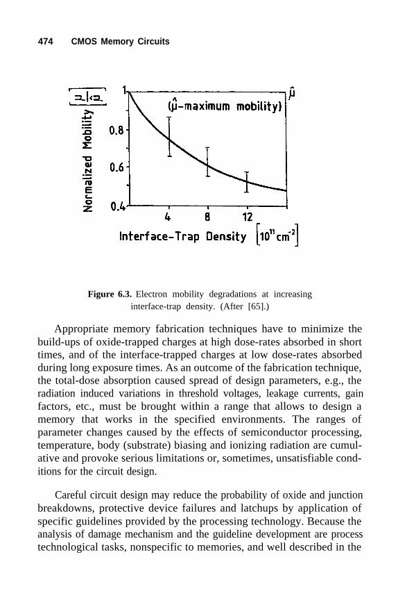
474 CMOS Memory Circuits
Figure 6.3. Electron mobility degradations at increasinginterface-trap density. (After [65].)
Appropriate memory fabrication techniques have to minimize thebuild-ups of oxide-trapped charges at high dose-rates absorbed in shorttimes, and of the interface-trapped charges at low dose-rates absorbedduring long exposure times. As an outcome of the fabrication technique,the total-dose absorption caused spread of design parameters, e.g., theradiation induced variations in threshold voltages, leakage currents, gainfactors, etc., must be brought within a range that allows to design amemory that works in the specified environments. The ranges ofparameter changes caused by the effects of semiconductor processing,temperature, body (substrate) biasing and ionizing radiation are cumul-ative and provoke serious limitations or, sometimes, unsatisfiable cond-itions for the circuit design.
Careful circuit design may reduce the probability of oxide and junctionbreakdowns, protective device failures and latchups by application ofspecific guidelines provided by the processing technology. Because theanalysis of damage mechanism and the guideline development are processtechnological tasks, nonspecific to memories, and well described in the

Radiation Effects and Circuit Hardening 475
literature [66]; the avoidance of breakdowns, protection failures and latch-ups are not discussed in this work.
To accommodate memory designs, the radiation induced variations inthreshold voltages and leakage currents are greatly reduced by theemergence of radiation hardened CMOS-bulk, CMOS SOI and CMOSSOS processes [67]. Depending on the processing technology, never-theless, circuit designs for a radiation dose of 106 rads (Si) still may haveto allow for large changes in n-channel threshold voltage VTN e.g., from0.6 V TN to 1.3VTN, in p-channel threshold voltage VTP e.g., from VTP to2.5VTP, for increases in drain-source leakage current I up to 200ILD LD andfor decreases in gain factor β down to 0.5β. Here, VTN, VTP, ILD and β arethe preradiation parameter values. These parameter changes are voltage-bias, temperature and annealing dependent and are nonuniform within thememory chip.
6.1.3 Transient Ionization Dose-Rate Effects
Transient ionization can be caused by both cosmic particle impacts andshort-pulse high-dose-rate nuclear radiation events, and conventionallyclassified as single-event and dose-rate phenomena, respectively. Singleevents can coerce erroneous data into the memory cells and peripheralcircuits locally, while dose-rate events can threaten the information storedand processed both locally and globally on the memory chip [68]. Bothlocal and global faults can manifest themselves in either soft or harderrors.
The failure mechanisms and error analyses, and the circuit technolo-gies to tolerate the effects of cosmic and package-emitted particle impactson memory circuits, are detailed previously (Section 5.3).
Short-pulse high-dose rate events affect the memory by generatinglarge temporary photocurrents and shifts in MOS device parameters, andalso by causing permanent damages in device material and latchups. Aftersome recovery time, the photocurrents and the device parameters returnapproximately to their predisturbance values. Nevertheless the disturbancecan cause a local loss of information in CMOS SOI (SOS) memories, andglobal data scrambling in CMOS-bulk memories. Local photocurrents

476 CMOS Memory Circuits
appear across each semiconductor junction in the circuit, but on thosesource-nodes of MOS devices which are connected to a power supply polethe photocurrents have insignificant effects on circuit operations (Figure6.4). Photocurrent simulations show that in a full-complementary storagecell fabricated on n/n+ epitaxial silicon substrate the well-photocurrent[69] is much larger than the other photocurrents in the cell (Figure 6.5).
Figure 6.4. Local photocurrent paths in MOS devices.
Figure 6.5. Well photocurrents in a 6-transistor CMOSmemory cell. (Source [69].)

Radiation Effects and Circuit Hardening 477
At low levels of expected photocurrents the information loss can beavoided by the use of state-retention memory cells (Section 9.23). How-ever, beyond some specific dose rate, e.g., 109-1010 rads (Si)/sec,photocurrents can be as much as 4mA/mm, transient threshold-voltageshifts can exceed the supply voltage and also other parameters may changeenormously. At this high rate of parameter changes the scrambling of datais seemingly unavoidable, but techniques for post-event data recovery areconceived and restricted to military use.
Operation during high-level transient events is usually unnecessary,because an external radiation detector may disconnect the memory fromthe system for the time of the exposure and recovery. An exposure to highdose-rates, however, may result in such thermodynamical stress that fusesinterconnects open or short, breaks loose bond wires, burns outsemiconductor junctions and destroys other circuit components.
6.1.4 Fabrication-Induced Radiations and Neutron Fluence
Fabrication of CMOS memories may involve the use of very energeticcharged particles and photons introduced by electron-beam and X-raylithographies, reactive ion, plasma and sputter etching, ion implantations,electron-gun deposition, and other radiation techniques. While thesetechniques satisfy stringent requirements in control of dimensional andmaterial characteristics, they can also cause radiation damages to thememory circuits while being fabricated.
The two most common effects of fabrication by radiation techniquesare the buildup of positive charges in the oxides and the increase in theinterface traps. The charge buildup in the oxide influences most signifi-cantly the threshold voltage and its long-term stability, and the interfacetrap increase can modify leakage currents, mobilities and other parameters.The fabrication-induced radiation effects are generally alleviated bythermal, hydrogen-assisted thermal and plasma annealing processes.Beside processing adjustments, the memory design does not have to useparticular circuit techniques to alleviate the effects of fabrication-inducedionizing radiations.

478 CMOS Memory Circuits
The effects of neutron radiation in CMOS memory circuits, up to afluence of 1015/cm2, are generally insignificant. Neutron fluence, however,degrades the lifetime of electrons and holes and, thereby, can causefailures in bipolar elements and circuits.
6.1.5 Combined Radiation Effects
A division of radiation-effect analysis into the areas of total dose,single events, dose-rate, fabrication-induced and neutron-fluence episodesis arbitrary. In reality, the effects of the various radiation types arecombined, because each of the radiation episodes leave an imprint in thememory and the radiation events join each to the other in certain extremeenvironments.
Typically, a satellite that applies memories may be affected byradiation total dose [611] in the Van Allen Belt, by cosmic particleimpacts [612] during orbiting in space, and to transient radiation [613] atan eventual hostile nuclear detonation. The radiation total dose effectsdecrease the operation margins (Sections 3.12 and 3.13) and, in turn, thedecreased margins make the memory circuits more susceptible to cosmicparticle impacts. Similarly, cosmic particles invariably deliver total dose,and so do the dose-rate phenomena that associated with nucleardetonations, and each of these events leaves less margin for total-dosetolerance (Section 6.2.2). During nuclear events the variety of phenomenaaffect the memory chips simultaneously.
The concept of combined phenomena may be examined through theeffects of an experimental irradiation with a single monoenergetic,homogenous beam. Experiments with proton and electron beams showthat proton-impact caused pulses degrade the data-upset threshold a lotmore than electron beams do at a given duty-cycle and an impulse length[614] (Figure 6.6). Short proton beam impulses, which deliver about 103
protons can upset the data stored in four-transistor-two-resistor 4T2Rmemory cells. Nevertheless, full-complementary CMOS six-transistor 6Tmemory cells show much less sensitivity to direct-ionizations fromprotons than 4T2R memory cells do, because, in most of the practical

Radiation Effects and Circuit Hardening 479
cases, CMOS 6T cells can recover much faster than the mean-time-be-tween-events MTBE in a proton-radiation environment.
Figure 6.6. Simulated data-upset thresholds of a 4T2R memory cellsversus pulse lengths of proton and electron beams. (After [614].)
Combined radiation events readily result in latchup and snapback.Possible latchup is inherent to CMOS structures, where the pnp and npnparasitic bipolar transistors form a pnpn semiconductor controlled rectifierSCR [615]. Normally, the SCR stays in its high-impedance state, but when(1) the loop gain, i.e., the product of the gains by npn and pnp transistors,exceeds unity, (2) the loop current achieves the SCR's exceed a certainturn-on (latch) limit, and (3) the voltage across the SCR is high enough tosustain the latch-situation, the SCR turns and stays latched in a low-resistance state (Figure 6.7) [616]. Exposures of the parasitic SCRs tocertain dose-rate ranges do, while to other dose-rate levels do not, result inlatchups in CMOS circuits. The latchup-free regions are called latchupwindows. Between the latchup windows the operation of CMOS bulkmemory can either entirely or partially impaired by switching the whole or

480 CMOS Memory Circuits
Figure 6.7. Current-voltage characteristics of a latchupsensitive CMOS structure. (After [616].)
an isolated well of the memory to permanent low-resistance conditions[617].
In a snapback phenomenon [618] the avalanche voltage VA is loweredinto the operating region of an n-channel MOS device characteristics(Figure 6.8) without any latchup effects. Unlike latchup, no positive feed-back loop exist to make the snapped back situation permanent [619]. Thus,a snapback state can be reversed, e.g., by bringing the drain-source voltageto zero.
By process technological approaches both the radiation inducedlatchup and snapback phenomena can be controlled, and the design has toassume a latchup and snapback free operation in the memory circuits.

Radiation Effects and Circuit Hardening 481
Figure 6.8. Current-voltage characteristics of a snapback-sensitiveCMOS structure. (After [618].)
6.2 RADIATION HARDENING
6.2.1 Requirements and Hardening Methods
Radiation hardening is the implementation of those of circuit-designand processing techniques which make a circuit able to operate or survivein a particular, or in a combination of ionizing radiation environments. Inspace and other nonmilitary electronics, rather arbitrarily, radiationhardened, radiation tolerant and commercial grade memory classes aredifferentiated to characterize the applied design and processing techniquesand the radiation environments in which the memory is able to operate(Table 6.1). Radiation hardened military memories have to satisfy strin-gent requirements not only in total dose and immunity against the effects

482 CMOS Memory Circuits
Applications RadiationHardened
Radiation Tolerant CommercialGrade
Design forSpecificRadiation Specific Nonspecific Nonspecific
Environments
Process forRadiation Specific Nonspecific Specific NonspecificEnvironments
Total Dose >200 10-200 <10[krad(Si)]
Threshold LET >80 50-80 <5[MeV/mg/cm 2]
SEU Error Rate <10-10 10- 10-10-5 >10-5[errors/bit/day]
Table 6.1. Radiation hardened, tolerant and commercialgrade memory characteristics.
of atomic particle impacts, but also in dose rate, neutron fluence and,eventually, in specific other parameters which relate to combined radio-active events (Table 6.2). Given parameters, i.e., single-event-upset (SEU),single-event-error-rate (SER), threshold linear-energy-transfer (LET), etc.(Sections 5.3.1 and 5.3.2), impose general requirements to reliable oper-ation in radiation environments and, together with all the other requisites,indicate whether and what specific hardening technique should be used.
Some degree of radiation hardness is inherent to all CMOS memorycircuits, but many applications in radiation environments call for theaddition of specific hardening techniques in either or in both processingand circuit design techniques. Thus, CMOS memories which can operatein radiation hardened environments may be obtained by the use of fourgeneral methods:

Radiation Effects and Circuit Hardening 483
(1) Radiation tests and screening of commercial-off-the-shelf(COTS) available memories,
(2) Process technological radiation hardening,
(3) Circuit technological radiation hardening,
(4) Combined process and circuit technological radiation hardening.
Military Radiation Hardness
Design Radiation Hard
Processing Radiation Hard
Total Dose >1 Mrad
Dose Rate >10 9 rad(Si)/sec
Neutron Fluence >10 15 neutron/cm2
SEU Error Rate <10-12 errors/bit/day
Threshold LET >150 MeV/mg/cm2
Table 6.2. Military radiation hardness.
The application of COTS circuits in radiation environments spurredthe development and use of sophisticated test and screening techniques[620]. Wide range of tests have shown that the down-scaling of featuresizes in CMOS fabrication technology increases the amount of totalradiation dose at which CMOS memories still can work. This improve-ment in radiation hardness is attributed mainly to the reduction in gate-oxide thickness and, in turn, to the decreased radiation induced thresholdvoltage variations. Although with down-scaling field-threshold voltagesdecrease and the effects of parasitic capacitances increase; the resultingaugmentation in leakage currents and crosstalk-signals can reasonably becontrolled by processing improvements.

484 CMOS Memory Circuits
Radiation hardened CMOS processing techniques [621] are vitallyimportant to keep radiation induced threshold voltage fluctuations, leakagecurrents, gain-factor degradations, crosstalk-signals and other parametervariations in small magnitudes, and to avoid radiation caused field-threshold voltage lowerings, latchups, snapbacks, thermo-electric andthermo-mechanic breakdowns, and other harmful effects. Furthermore, theeffects of incident atomic particles and transient dose-rate phenomena onmemory reliability, can be greatly reduced by the application of ahardened CMOS SOI or SOS technology in place of a traditional CMOS-bulk technology. Radiation hardening of CMOS processings has emergedas a significant and elaborated area of semiconductor fabrication, and ithas evolved as a driving force to SOI and SOS process developments.Process hardening often involves (1) the development of high-quality verythin channel-oxides to reduce transistor threshold voltage variations,(2) doping profile control for transistor and field-threshold voltageadjustments and for leakage current minimization, (3) low temperaturefabrication for better parameter control and for decrease of process-causeddamages, (4) a variety of annealing techniques to decrease parameterspreads and to improve device reliability, and (5) other technologicalmethods. Additionally, SOI and SOS processing techniques provide verysmall active device area and allow for full-oxide isolations amongtransistors and wirings. Moreover, the formation of transistors in SOI andSOS technologies do not require the use of p- and n-wells; and the lack ofwells reduces the path-lengths of incident atomic particles in silicon, anddecrease the probability of local latchups which may be caused by high-energy transient radiations.
Radiation hardening through circuit design techniques [622] createcircuits which are able to accommodate the total amounts of parametervariations resulting from the effects of various radioactive events and fromthe fluctuations of CMOS processing, power supply, device bias,temperature, hot-carrier emission, and other parameters. The very largeparameter-spread that has to be tolerated by a radiation hardened memorycircuit, and the parameter-spread tolerance requirements for nonhardenedoperations, may be exemplified in a comparison of threshold voltageranges for hardened and nonhardened designs (Figure 6.9). For hardeneddesigns, in addition to the capability of operation with greatly extended

Radiation Effects and Circuit Hardening 485
threshold voltage fluctuations, the targets and spreads of both thresholdvoltages should be adjusted to obtain reasonable ranges for operation and
Figure 6.9. Threshold voltage ranges for hardenedand nonhardened designs. (Source [622].)
noise margins. Reduced margins and shifted margin-ranges decrease andlimit the levels of total doses at which the circuit is able to operate, andincrease the susceptibility of the memory to both atomic particle impactsand dose-rate type of transient radiation events. To improve radiationhardness CMOS memory designs apply (1) full-complementary staticdigital circuits to implement Boolean- and sequential-logic requirementsand (2) full-complementary static six-transistor (6T) memory cells for datastorage and in flip-flops. The large operation and noise margins of full-complementary logic and storage elements are unmatched by the senseamplifiers. To improve the operation and noise margins of irradiated sensecircuits, the design may feature (1) self-compensation, (2) voltage-bias

486 CMOS Memory Circuits
limitation and (3) parameter tracking and eventual other radiationhardening measures. For mitigation of the effects of transient radiationsand atomic particle impacts the use of (1) state-retention memory cells(Section 5.3.3), and (2) CMOS SOI (SOS) process and circuit tech-nologies, are preferred. If the peripheral logic circuits also need improvedradiation hardness, logic gates which adjust their operation characteristicsto radiation induced parameter changes, may be employed. For generalradiation hardness improvements however, the implemen-tation of fault-tolerance (1) by memory self-repair (Section 5.6) and (2) by error controlcoding (Section 5.7) have emerged as the most effective and mosteconomical circuit techniques, so far.
Because processing techniques are not subjects of this book, and theproperties of full-complement digital logic circuits are widelypublished; the following sections focus on the radiation hardening of sensecircuits and memory cells, reviews the radiation hardness enhancement oflogic gates, and briefs the use of fault-tolerance techniques (Sections 5.5-5.8) to radiation hardened CMOS memories. Additionally, the mostimportant issues of the application of CMOS SOI (SOS) processingtechnologies to memory designs are described in the final sections of thischapter.
6.2.2 Self-Compensation and Voltage Limitation in SenseCircuits
The sense circuit has, historically, been the most susceptible memorycircuit to both uniform and nonuniform parameter changes, and, thus, tothe effects of radioactive irradiations. Memories, which have to operate inradiation hardened environments, use symmetrical differential amplifiers(Sections 3.2-3.5) to sense data generated by full-complementary staticmemory cells. Postradiation internal operating margins of sense circuits(Figure 6.10) in typical static memories, even which are fabricated withradiation hardened processing, may disappear already at low radiationdoses [623]. This is chiefly because of the effects of radiation-inducedincreases in circuit imbalances, leakage currents, and charge transfers. Theimbalance increase is a result of nonuniform bias dependent changes inthreshold voltages and carrier mobilities; the high leakage-currents are

Radiation Effects and Circuit Hardening 487
caused mainly by the enlarged subthreshold drain-source and device-to-device parasitic currents; and the charge transfer increase is an effect of
Figure 6.10. Operation margin degradations in an SRAM sense circuitwith p-channel memory-cell access devices. (Source [623].)

488 CMOS Memory Circuits
variations in MOS capacitances. To reduce the radiation sensitivity ofCMOS symmetrical differential sense amplifiers, self-compensation andvoltage-bias limitation can be used in the sense circuit.
Imbalances in a symmetrical sense circuit appear as sense amplifieroffsets. Thus, all of the offset reduction techniques (Section 3.5) can alsobe applied for radiation hardening of sense amplifiers. Radiation inducedparameter changes can most effectively be compensated by negativefeedback, sample-and-feedback and by other sense amplifiers which haveinherent offset compensation capability.
Figure 6.11. Negative feedbacks in sense amplifier for offset reduction.(Source [319].)

Radiation Effects and Circuit Hardening 489
From the variety of sense amplifiers which use negative feedback foroffset reduction (Section 3.5) the most suitable ones for radiationhardening are those in which the constituent MOS devices function undersmall bias voltages (Figure 6.11). At small drain-source, drain-gate andsource-gate voltage differences, namely, the radiation induced parameterchanges are significantly reduced. In these amplifiers voltage biases arereduced because (1) the drain-source and gate-source voltage drops on theindividual MOS transistors are fractions of the supply voltage, (2) thesignal amplitudes on the gates of the input and output transistors are small,and (3) the clock-impulse amplitudes may also be small. Because of thesmall output signal amplitudes these feedback circuits are applied often aspresense amplifiers and followed by a low-sensitivity large-signal senseamplifier. The susceptibility of these differential sense amplifiers toparameter variations may greatly be decreased by the application ofnegative feedback (Section 3.5.3). Negative feedback in the pre-senseamplifiers are provided by resistors R1-R4 or transistor devices MP5,MP6, MN7, and MN8. These feedback devices must be designed so thatthe negative feedback effectively compensates certain limited offset, butthe circuit remains still capable to amplify the signal that is generated bythe spatially most remote cell to an acceptable amplitude to the follow-upamplifier.
A sample-and-feedback amplifier (Figure 6.12) is virtually free fromthe tradeoff between offset-reduction and signal-amplification, but it israther complex and the sampling requires extra time. This amplifier takessample voltages from the precharged pair of bitlines or from the outputnodes, applies these voltages or the output voltages to the gates ofregulator devices MP5, MP6, MN7, MN8 through coupling transistorsMP9, MP10, MN11, MN12, and stores the sample voltages on the gatecapacitances of the regular devices. Because the sample voltages on thegates of the regulator devices change the individual drain-source resist-ances of these devices so that they act against an eventual output voltagedifference, the sense amplifier compensates, in some degree, the effects ofits initial imbalances. The accuracy of compensation depends mainly onthe symmetry of the regulator device pairs. To reduce non-uniform deviceparameter changes caused by radioactive irradiations, the sample-and-

490 CMOS Memory Circuits
feedback amplifier designs may also use voltage limitations in the ampli-tudes of the input and output signals.
Figure 6.12. A sample and feedback sense amplifier. (After [538].)
Voltage amplification combined with negative feedback or sample-and-feedback have proved to be adequate to satisfy many radiation hard-ening requirements. Beyond the usual requirements in combining highpacking density, operational speed and radiation hardness, the use of thecurrent sense amplifiers, with inherent capabilities for imbalancecompensation (e.g., Section 3.4.4), becomes increasingly attractive.

Radiation Effects and Circuit Hardening 491
6.2.3 Parameter Tracking in Reference Circuits
Parameter tracking is the capability of a circuit to adjust its operatingregion in accordance to changes in one or more MOS device parameters. Atracking of the average change of threshold voltages in the access devicesof the memory cells can considerably improve the radiation hardness of amemory by making the precharge voltage a function of the total dose insense circuits (Figure 6.13).
Figure 6.13. Precharge voltage tracks radiation inducedthreshold voltage variations.
In sense circuits, to which the precharge voltage VPR is provided by adivision of the supply voltage (Sections 3.1.3.7 and 4.2.2) and VPR doesnot track threshold voltage changes, the variation range of the prechargevoltage, i.e.,

492 CMOS Memory Circuits
is determined by the division factor ρd that has very little fluctuation ∆ρ d asthe total dose absorption changes, and ∆ρ follows the variations of thed
supply potential difference (VDD-VSS). Namely, the division of (V DD-V SS) isimplemented in nonhardened designs as a resistive or capacitive dividercircuit to provide a stable VPR that is minimally influenced by deviceparameter changes. In sense circuits, this stability of VPR may lead todramatic decrease of the 0 or 1 operating margin at low radiation doses,because the operating margins bend as the threshold voltages of thememory cells access devices vary with the absorbed total dose.
Precharge voltage can also be obtained by deducting one or morethreshold voltage VT from the supply potential (Section 4.2.2). In this case,the precharge voltage and its range follow the threshold voltage variations
Since threshold voltage variations ∆VT-s are greatly radiationdependent, VPR can be designed to track the radiation induced changes inVT , so that the decrease in operating margins at increasing doses ismarkedly less than that provided by divider circuits.
For the adjustment of operating margins the output voltage of aprecharge generator circuit VPR(t) (Figure 6.14) should follow approx-imately the radiation-induced variations in the threshold voltage oftransistor MN1 and of the access transistors of the memory cells, whichare under the same voltage bias conditions during data storage. For MN1,the worst appearing bias combination in radiation environments,i.e., V S = VSS, V DS = VGS = VDD , is provided when clock φPR turns devicesMP2 and MN3 on and, thereby, the drain and the gate of MN1 are coupledto the positive supply voltage VDD and the source of MN1 is connected toV SS . Here, VS , VDS and VGS are the source, drain-source and gate-sourcevoltages for the transistor MN1. At precharge, transistor MN4 is broughtto highly conductive state, MP2 and MN3 are turned off, and after atransient time, a precharge voltage

Radiation Effects and Circuit Hardening 493
occurs. Here, R1 and R2 are the voltage-divider resistances, rd4 is the drain-source resistance of MN4, V is the n-channel threshold voltage and VTN BG
is the backgate bias of MN1. Since the bias of MN1 mimics the worst casebias of the access devices of memory cells, the output voltage of thegenerator and the precharge voltage follow the worst-case radiation-induced changes in the threshold voltage. Similar tracking of thresholdvoltage changes can be designed to enhance the operating margins ofsense circuits, which contains p-channel access devices to the memorycells (Section 4.2.2).
Figure 6.14. Threshold-voltage-tracking precharge generator circuit.
6.2.4 State Retention in Memory Cells
For the design of radiation hardened memories the choices are the full-complementary static six-transistor 6T types of memory cells (Section2.4). These 6T memory cells can tolerate the largest amount of deviceparameter changes, and provide the largest operating and noise marginsamong all types of memory cells when applied in arrays. Furthermore,

494 CMOS Memory Circuits
their application in memories is compatible with fast write and readoperations, they retain data despite the appearance of high perturbingcurrents, their sizes are acceptably small and they are readily availablefrom mainline nonhardened memory designs.
Total dose hardness of a large memory cell array may be extended byusing p-channel access devices in the 6T memory cell (Figure 6.15). Whenradiated, threshold voltages in p-channel devices tend to be more negativeunder any bias condition, while n-channel threshold voltages may increaseor decrease (Section 6.1.2). As an n-channel transistor's threshold voltagedecreases, the subthreshold drain-source current of the memory-cellaccess-devices may increase to an amount that can perturb the datumstored in the memory cell (Section 3.1). The chances of subthreshold-current-generated perturbations are much less at the use of p-channelaccess devices than those at the application of n-channel access transistors.
Figure 6.15. RC elements and p-channel access devices in a six-transistorstate-retention memory cell.

Radiation Effects and Circuit Hardening 495
Dose-rate and atomic-particle-impact caused data loss or scrambling maybe reduced or avoided by applying an additional capacitor C and tworesistors R to the 6T memory cell (Section 5.3.3). For C the dielectricmaterial is a high quality thin oxide, and R is formed of doped polysilicon.Preferably, both the plates of C and all surfaces of R should interface with
dielectrics to keep the time constant τ = RC large when radiation-induced
spurious currents appear. A sufficiently large τ disallows the completecharge or discharge of C during transient radiation events, and the chargeremaining on C should be capable to return the memory cell to itspreradiation stable state after the effects of the transient radiation abate.
Transient radiation hardness may be aggrandized by fabricating thememory that combines RC enhanced 6T state-retention memory cells withSOI or SOS processing. CMOS SOI and SOS structures greatly decreasethe charge collection paths of incident radioactive particles and eliminatedevice-to-device currents through pn junctions. Nevertheless, side andback channel parasitic currents and uncontrolled charge buildups in thechannel substrates may cause significant difficulties in designs with SOIand SOS devices (Section 6.3). Despite the superior radiation hardness ofCMOS SOI and SOS six-transistor 6T static memory cells, there is atendency to use one-transistor-one-capacitor 1T1C dynamic memory cells(Section 2.2) wherever it is possible, due to the small size of the 1T1Cmemory cell implementations. To improve radiation hardness in a 1T1Cmemory cell, the cell-internal storage capacitor may be expanded and a p-channel access device may be applied.
State retention in memory devices may be provided also by theapplication of circuit elements other than capacitors and resistors, e.g., byEPROM, EEPROM, etc., components. These electrically programmablecomponents are radiation sensitive. Radiation hard, however, are theFRAM (Section 2.2.4.2) components, which have great potentials for usein future radiation hardened memory devices.
6.2.5 Self-Adjusting Logic Gates
In CMOS memories the full-complementary static peripheral digitalcircuits, usually, do not require specific circuit techniques for the increase

496 CMOS Memory Circuits
of radiation hardness, because they are less sensitive to total dose effectsthan the sense circuits, because they do not have to store data duringradiation events, and because they do not require to operate duringtransient dose-rate episodes. Nevertheless, when operating at high totaldoses, their input-output voltage characteristics may be modified and theirnoise margins may considerably be reduced (Figure 6.16) as results of theradiation-induced threshold voltage changes and of the drain-sourceleakage-current increase in the n-channel devices (Section 6.1.2).
Figure 6.16. Pre- and postradiation input-output characteristicsof a CMOS inverter.
This radiation induced noise margin reduction can be compensated.The compensation does not have to retain the circuit's preradiation transfercurve, but it should keep the noise margins larger than a predeterminedextent through the entire total dose region in which the memory shouldoperate.

Radiation Effects and Circuit Hardening 497
In peripheral digital circuits of memories, a single resistor R ortransistor device MN5 that is added to an inverter or logic gate (Figure6.17) may be sufficient to counteract the noise-margin modifying effectsof the changes in threshold voltages and in leakage currents. In thesecircuits the threshold voltages VT (VBG) of the n-channel transistor MN1get elevated when the substrate or backgate bias VBG increases due to acurrent increase. When the drain-source current i dl of the n-channel deviceMN1 increases due to a radiation induced threshold voltage lowering ∆V'T,then node potential VR, substrate bias VBG and, thereby, the postradiationV' ) also tend to increase. Thus, the bias-dependent threshold voltageT(V BG
increase ∆VT can compensate the radiation induced reduction ∆V' T
through an appropriately designed resistor R coupled to the source of then-channel devices. Resistor R may be implemented in a polysiliconresistor, or in an n-channel transistor device MN5 that operates in its trioderegion. To MN5, triode-operation may be obtained by the use of a fixedgate voltage, e.g., VDD, or by the application of gate voltage VPR whichtracks the radiation-induced threshold voltage variations (Section 6.2.3).
Figure 6.17. Counteracting radiation-induced shifts in input-outputcharacteristics of inverters and logic gates.

498 CMOS Memory Circuits
More complex circuit variations for input-output characteristics andnoise margin adjustment, e.g., requiring three additional transistors perlogic gate plus radiation tracking ∆V'T and preradiation V(Figure 6.18) [624],may also be considered. In this circuit, a compensation
Tgenerators
in postradiation input-output voltage characteristics and in noise margins
Figure 6.18. Noise margin adjustment in an inverter. (After [624].)
can be provided, if the gain-factor ratio β4/β3 = 4. The desirability of thisratio may be substantiated by the equation of the currents through deviceMN3 and MN4 when A is a log.0:
where β3 and β4 are the gain-factors of MN3 and MN4, VG is the gatevoltage, Vx is the voltage on node X, and postradiation threshold voltageVT is assumed to be approximately the same for MN3 and MN4. Becausein radiation environments VT-s, ∆ VT-s and β-s change nonuniformly and a

Radiation Effects and Circuit Hardening 499
preradiation V is difficult to maintain, the effectiveness of this circuit isT
very limited in improving radiation hardness.
6.2.6 Global Fault-Tolerance for Radiation Hardening
Radiation hardness of CMOS memories can greatly be enhanced bydesigning fault-tolerant features globally in the memory chips. In radiationhardened memories fault-tolerance is achieved by either one or by thecombination of the following approaches:
(1) Error control coding,
(2) Fault repair,
(3) Fault masking.
Error control coding (Section 5.7) is used to detect and correct many ofthe random soft-errors induced by cosmic particle impacts and dose-rateevents, and some of the hard errors resulting from the effect of total-doseand dose-rate type of radioactive radiations. Effects of radiations mostcommonly detected and corrected by
Single error correcting bidirectional parity (imparity) check code,
Two to four error correcting Hamming codes,
Burst correcting Berger codes.
Implementations of other codes which provide higher performance,e.g., Reed-Solomon, Viterbi codes, require such excessive layout areasthat their on-chip applications appear to be uneconomical beyond about0.2µm processing feature sizes.
Fault repair techniques (Section 5.6) replace the permanently damagedrows, columns and clusters of memory cells by operating circuits.Replacements of faulty circuits are usually applied to avoid the overrun ofthe capabilities of an error correcting code and to repair origins of errorswhich are uncorrectable by codes. The most successful repair techniquesare implementation of the associative approach (Section 5.6.4).

500 CMOS Memory Circuits
Fault masking (Section 5.6.5) is a convenient approach to improve thereliability of the peripheral circuits beyond the reliability of the memorycell array, and to render the control circuits, which provide fault-tolerance,insensitive to their own faults. For fault-masking the triplicate majoritylogic is the nearly exclusive choice, but for repair of the input and outputbuffers duplication seems to be the practical approach.
Figure 6.19. Architecture of a radiation hardened CMOSstatic memory. (Source [625].)

Radiation Effects and Circuit Hardening 501
The combination of all approaches fault-tolerance, hardened sub-circuits and hardened processing is required to provide a high level ofradiation hardness in memories. A heavily radiation hardened memoryarchitecture (Figure 6.19) [625] comprises a main memory cell array, aspare memory cell array, duplicated error control coding ECC and ECCR,duplicated output circuit OUT and OUTR, a control circuit of repairs foryield improvement REP, a control circuit to provide associative iterativerepair for reliability increase AIR, built in test generator and control circuitTEST and other circuits. In this memory, all circuits except the memorycell arrays and except the output buffers, are implemented in triplicatedmajority-voting logic circuits. In spite of circuit triplications andduplications and the accommodation of fault tolerance and self-test, theperipheral circuits take only about 4%, while the spare memory occupiesapproximately 7% of the memory chip. This memory architecture isdeveloped for applications in military satellites.
6.3 DESIGNING MEMORIES IN CMOS SOI (SOS)
6.3.1 Basic Considerations
6.3.1.1 Devices
CMOS SOI (SOS) processing and device technologies are the mostwidely used derivatives of the basic CMOS-bulk technology. In additionto improved radiation hardness the feature sizes of CMOS SOI (SOS)transistor devices are readily scalable to well below 0.1µm, while a featuresize of 0.12µm seems to be the lower practical limit for the down-scalingof CMOS-bulk transistor devices. This amenability of CMOS SOI (SOS)transistors to down-scaling greatly increases the future potentials ofCMOS SOI (SOS) technology applications not only in radiation harden-ing, but also in general integrated circuit processing and manufacturing. Insome aspects, CMOS SOI (SOS) processing and device technologiesdeviate from CMOS-bulk technologies, and the deviations effect the char-acteristics of both the active and passive circuit elements. In circuitdesigns, the structures and properties of the elements which are effected bythe use of nonstandard CMOS technologies, must be taken into consider-ation.

502 CMOS Memory Circuits
The technology that implements complementary metal oxidesemiconductor (CMOS) transistor devices in semiconductive siliconislands on an insulating layer, rather than directly on a semiconductivesilicon bulk, is called CMOS silicon-on-insulator (CMOS SOI) technology[626]. The early CMOS SOI technologies used sapphire as insulating basisand, therefore, the technology was named CMOS silicon-on-sapphire(CMOS SOS) technology [627]. Somewhat imprecisely, the term CMOSSOI is used also to distinguish the technology that applies an insulatorlayer on a bulk silicon from the CMOS SOS technology. Commonly,CMOS SOI (Figure 6.20a) applies a SiO2 layer between the MOSFETdevice and the carrier substrate-semiconductor. The semiconductor carrier
Figure 6.20. Cross-sectional views of an n-channel transistor fabricated withSOI (a) and SOS (b) technologies.

Radiation Effects and Circuit Hardening 503
substrate readily allows for creation of oxide isolation among the semicon-ductor MOSFETs and other devices. In CMOS SOS, the device-to-deviceisolation in CMOS SOS (Figure 6.20b) is provided by the sapphiresubstrate and by the oxide developed on the surfaces of the semiconductorislands.
In semiconductor islands the CMOS transistors can be implemented tooperate in a variety of modes, e.g., in partially depleted (PD), fully de-pleted (FD), dynamic threshold (DT), and other operation modes, whichallow to meet diverse technical requirements. In a PD device, the electricfield of gate depletes the silicon body only to a depth that is less than thethickness of the silicon film. Because of the limited depth of the depletionregion PD devices operate similarly to traditional bulk devices. Thus, formemory designs with PD devices, the circuit and design techniques of themainline CMOS-bulk technologies can be adopted. Although CMOS-bulktransistor models have to be somewhat modified, mainline design toolsand methods are also applicable to PD CMOS SOI (SOS) memory cells.PD devices combine high drain-source currents and radiation hardness,and make possible to produce high-performance memory devices whichcan operate in severe environments. In FD devices the total depletioncharge, including front, back and lateral depletion charges, exceeds thepossible depletion charge in the silicon body. The total depletion results inlow subthreshold leakage currents and large drain-source resistances in thesaturation region. Low leakage currents are important for the operation ofthe access transistors in memory cell arrays (Section 3.1.3.3), and toachieve low standby power dissipations, while high resistances in thesaturation regions facilitate high gains in sense amplifiers (Sections 3.3,3.4 and 3.6) and in analog devices (e.g., Section 3.3.6.4). In DT devices,the gate is connected to the body and, thereby, activate the parasiticbipolar transistor. The operation of the bipolar transistor increases thecurrent between the drain and source and reduces the threshold voltage ofthe CMOS SOI (SOS) device. The threshold voltage decreases due toforward biasing the body-source or the body-drain diode. Currents throughthe diodes contribute to the standby current, limit the number of memorycells coupled to a bitline, and increase sense amplifier offsets. Further-more, the increased body potential may enlarge the diodes junctioncapacitances.

504 CMOS Memory Circuits
In CMOS SOI (SOS) memory technology, the high current drivecapabilities of PD devices, the low subthreshold leakage currents and highsaturation resistance of FD devices, can be combined by switching betweenPD and FD operation modes. For the implementation of PD-FD switchingin dual-mode transistors the polysilicon backgate technique (Figure6.21a) has great potentials, because the implementation of the PD-FDswitch effects the packing density very little, its integration into theprocessing is not difficult, and it can be used also for threshold voltageswitching and control. Dual threshold voltage application may be neces-sary in the designs of the memory cell arrays and sense circuits, especiallyin designs for low voltage operations. Array designs may have to applybootstrapped wordline drivers, the boosting capacitor may also be imple-mented in CMOS SOI (SOS) at small modification in the polysiliconbackgate technique [628] (Figure 6.21b).
Figure 6.21. Backgate (a) and boosting capacitor (b) implementations.
In the following, the CMOS SOI (SOS) transistors are understood tooperate in the partially depleted mode unless the text designates theoperation mode of CMOS SOI (SOS) transistor device otherwise.

Radiation Effects and Circuit Hardening 505
6.3.1.2 Features
The interest in making CMOS SOI (SOS) memories has been spurredby the anticipation of significant improvements in (1) radiation hardness,(2) operational speed, (3) power dissipation, and (4) packing density, incomparison to those provided by CMOS-bulk memories.
Radiation hardened memory designs use CMOS SOI (SOS) techno-logies to greatly reduce the number of single event errors and theprobability of latchups which may be caused by the impacts of ionizingatomic particles, by transient dose-rate events and by permanent total-doseionization. Incident ionizing particles find much shorter charge collectionpaths S-s and produce much lower single event error rates in CMOS SOI(SOS) than in CMOS-bulk designs. Taking the sensitive regions asparallelepipeds, then the approximate maximum in a CMOS SOI (SOS)transistor is
while that in a CMOS-bulk transistor is
Here, W and L are the width and length of the transistor drain- orsource-area, d is the depth of the depletion region, and t s is the thickness ofthe semiconductor film. In practice, t <<L+2d, thus . A parasitics
bipolar transistor amplifies the charge Q that is induced by the incidenti
atomic particle along S, by a factor of (1+βx ), where βx is the effectivecharge gain. Thus the charge collected by the drain Q may be approxi-d
mated by [629]
and
Q = K·S·LET ,i
where K is a constant, and LET is the linear energy transfer. To alter adatum in a memory cell LET = LET and Q = Q required, where LET isC d c C

506 CMOS Memory Circuits
the critical LET, and QC is the critical equivalent charge. Applying theequation for Qi the LETC may be given as
The expression of LETC indicates that for large LETC and, in turn, forhigh immunity against the effects of incident atomic particles, large Qc ,small S and small βx are required. Since the charge collection paths S-s aresignificantly smaller in CMOS SOI (SOS) memories than those in CMOS-bulk memories, CMOS SOI (SOS) memories can operate at much lowerSEU rates than CMOS-bulk memories do in radiation environments.Furthermore, in CMOS SOI (SOS) circuits the complete insulation ofsemiconductor transistor devices and the use of highly doped semi-conductor interconnects, eliminate the inadvertent creation of largeparasitic bipolar transistor and thyristor devices and, thereby, avoid thepossibility of global latch-ups which can be induced by transient dose-rateevents. Although latch-ups may occur locally in those silicon islandswhich include a pnpn structure, many of the local failures can be toleratedin memories by the application of error detecting and correcting codes andfault repair circuits. Since radiation hardened memory circuits have beenindispensable in satellites, missiles, rockets, high-altitude aircraft and avariety of space, high atmospheric and military equipment, the evolutionof CMOS SOI (SOS) technologies have been well supported.
The anticipation of high speed in CMOS SOI (SOS) memory opera-tions is based on the effects of the rather small parasitic transistor- andfield-capacitances, and of the low effective threshold voltages. Parasiticcapacitances in the CMOS SOI (SOS) transistors are quite small becausethe drain-body and source-body junction areas are very little, and becausethe substrate is isolated from the transistors. Field, i.e., substrate-wiring,capacitances may also be small because the thickness of the insulatorbetween the carrier substrate and the silicon film adds to the thickness ofthe oxide between the wires and the insulator surface. CMOS SOI (SOS)n-channel transistors, which are placed on silicon island have littlethreshold voltage increases during operations because the backgate biasvoltages are mostly such that they reduce rather than increase the effective
Radiation Effects and Circuit Hardening 507
threshold voltages. Low threshold voltages result in high effective gate-source voltages and, in turn, in high drain currents, which are particularlyimportant in output drivers and NAND type of decoder and logic circuitdesigns. In practical circuits, however, the speed-increasing effects of thesmall parasitic capacitances and threshold voltages are upset by the speed-reducing effects of the floating substrates, charge-carrier mobilitydegradations, eventual side- and back-channel currents, threshold voltagefluctuations caused by film thickness variations, reduced field oxidethickness, and other CMOS SOI (SOS) phenomena. Thus, the speed ofCMOS SOI (SOS) memories are only 25-35% faster than the speed ofCMOS-bulk memories. This speed gap is anticipated to increase withdecreasing feature sizes in the deep submicrometer region, where theparasitic capacitances in CMOS SOI (SOS) reduce in greater percentagethan those in CMOS-bulk devices do.
The expectation for low power consumption in CMOS SOI (SOS) isindicated also by the small parasitic capacitances and by the low effectivethreshold voltages. Small capacitances need small energy to charge anddischarge, and low effective threshold voltages allow the use of lowsupply voltages. Capacitances proportionally and supply voltages quadra-tically effect the dynamic power dissipation, thus their reduction can sub-stantially decrease the total power dissipation. Nevertheless, in CMOS SOI(SOS) memories the reduction of the total power consumption is limitedby the substantial wire-island capacitances, threshold voltage variationsand subthreshold currents. The anticipated improvement in control ofthreshold voltages and subthreshold currents may make the use of CMOSSOI (SOS) technology more attractive also for memory designs.
Device packing densities in CMOS SOI (SOS) memories can signifi-cantly be higher than those in CMOS-bulk memories. CMOS SOI (SOS)circuit implementations, namely, do not need wells and well separations,and CMOS SOI (SOS) processing are very amenable to fabricate stackeddevice structures.
Generally, the use of CMOS SOI (SOS) processing technology defi-nitely results in high radiation hardness and packing density, but theanticipated advantages in operational speed and power dissipation may notbe significant enough to justify the higher production costs. CMOS SOI

508 CMOS Memory Circuits
(SOS) production costs are high, not only because of the expensivestarting material, but also because the processing equipment, and theengineering and design tools deviate from the CMOS-bulk standards in anumber of aspects.
Memory circuits applied in CMOS SOI (SOS) designs are nearlyidentical with those used in standard CMOS-bulk technologies. CMOSSOI (SOS) memory designs, nevertheless, have to overcome the effects ofthe (1) floating substrates, (2) side- and back-channels, and (3) diode-likeparasitic elements and others, which should be taken in account in thedesigns despite improvements in CMOS SOI (SOS) processing technolo-gies, e.g., [630].
Additionally, designs of certain CMOS SOI (SOS) circuits may bevery complex due to the self-heating of the transistor devices on insulatingsubstrates [631]. Unlike the standard CMOS transistor devices which areplaced on a common semiconductor substrate in a chip, the individualCMOS SOI (SOS) transistors are isolated dielectrically and thermo-dynamically from a common substrate and from their adjacent elements.The small thermal-conductance of the insulating material in the vicinity ofa transistor device may allow for substantial temperature elevation whenthe transistor operates at a high drain current. A temperature-changeinfluences important device parameters, e.g., threshold voltage, gainfactor, etc., which, in turn, vary the drain-current. Because of theinterdependency between the drain-current and temperature, the operatingtemperature of numerous transistor devices should individually becalculated. For computations and mappings of device temperatures on aCMOS SOI (SOS) chip, computer programs are available, and allow forcombining temperature variations in individual transistors with electriccircuit analysis, e.g., [632]. High operating temperatures of transistors mayimpose substantial constraints to the layout designs, and may require thedesign of thermo-specific structures and the combination of thermal-conductors and thermal-shields with electric circuit elements. Nonetheless,in memory-internal circuits, i.e., memory cell arrays, sense circuits,decoders, input interface and peripheral logic circuits, the self-heatingeffect causes only a small, e.g., 8°C, temperature raise. Thus, thermaleffects may significantly influence the design of the output buffers and

Radiation Effects and Circuit Hardening 509
direct-current reference circuits, but may result only in insignificant timingand performance variations in all other memory circuits.
6.3.2 Floating Substrate Effects
6.3.2.1 History Dependency, Kinks, and Passgate Leakages
Floating substrate, or floating body, means that the channel region of aMOS transistor has no low-resistance connection to any fixed potentialsource such as ground VS S , power supply VD D or V CC . The lack of wiring ofthe channel regions to VS S , VDD or V C C results high packing density, butalso makes the potential of the channel region of each individual transistordifferent from each other, depending on their drain-, source- and gate-potentials as well as on the time of observation and the potential variationsbefore the observation, Effects of the floating substrate and of theconsequent substrate potential changes in a CMOS SOI (SOS) transistormay result in the occurrence of (1) history or time dependency of thresholdvoltages VT (t)-s and (2) kinks and premature breakdowns in the directcurrent DC drain-current ID versus drain-source voltage VD S and gate-source voltage VG S characteristics I D = f (V
D S, VG S ), and (3) transmission or
passgate leakage currents [633].
The history or time dependent characteristic of VT (t) may be taken inaccount by the variations of the backgate bias as a function of timeVB G (t) (Figure 6.22), because VT [VG B (t)]. At a particular time t, VB G (t) isdetermined by the signals which appeared prior to the observation time onthe device’s drain, gate- and source-terminals, by the device-internalcharge and discharge times and by the generation and recombinationmechanisms of the electrons and holes. Within a CMOS SOI (SOS)transistor device (Figure 6.23) capacitances CDB , C GB , C CB and CSB arecharged and discharged through capacitances CGD , C DS , C GC and C GS ,diodes DD B and DS B , resistances RD , RS , RD B , RS B , RBD and R B S, and bipolarjunction transistor (BJT) TD B S . Here, for a capacitance C, diode D andtransistor T the indices D, S, G, B and C designate drain, source, gate,body and channel of a CMOS SOI (SOS) device, respectively. Signal

510 CMOS Memory Circuits
Figure 6.22. Simulated backgate bias as a function of time inan n-channel SOI transistor
variations, on the terminals of a CMOS SOI (SOS) transistor, change thedevice-internal voltages and currents, which changes induce differingdevice-intrinsic charge and discharge times and differing carrier gener-ation and recombination mechanisms. These differing events result in ahysteretic behavior in VT [VB G (t)] when the device is controlled by animpulse that has symmetrical rise and fall transients. The hysteresis inVT [VB G (t)] affects the signal delays at small control signal amplitudes Vo - sand at low supply voltages VD D -s significantly more than at large V -s ando
high V -s, because the switching times are functions of the terms VDD o -V T[VB G (t)] and VD D-V T[VB G (t)], where Vo ≈ VD D > V T [VB G (t)].

Radiation Effects and Circuit Hardening 511
Figure 6.23. A model of parasitic elements present in a CMOS SOI(SOS) transistor device.
Time dependency and hysteresis in VT [VB G (t)]-s can lead to incorrecttiming and undesirable race conditions for clock, control and general logicsignals, operation and noise margin degradations, read and write patternsensitivities, increased sense and small-signal amplifier offsets, and toother type of inadequacies in circuit operations. The timing of memorysubcircuits and the propagation delays of the clock signals, in addition toothers, are influenced also by the VT [V B G (t)] variations of the individualtransistor in the drivers and in the receivers. Increased variations in thesignal delays may result in incorrect activation of subcircuits and inerroneous output signals in logic gates. In sense circuits VT [VB G (t)]decreases may particularly be harmful because low VT [V B G (t)-s areassociated with large subthreshold leakage currents in the access devices.The enlargement of leakage currents degrades the operation and noisemargins, may cause false reads or writes, and may make the read and write

512 CMOS Memory Circuits
operations pattern sensitive in memory cell arrays (3.1.3.3). Read andwrite operations, furthermore, may significantly be slowed or impaired bythe nonuniform VT [V BG(t)] variations caused offset augmentations in dif-ferential sense amplifiers (Sections 3.1.3.5 and 3.5). The possible overalleffects of VT[VBG(t)] variations include increased read and write errorrates, degraded radiation hardness, longer access- and cycle-times, exces-sive power dissipation, unreliable memory operation and impaired func-tionality.
Memory operations may adversely be influenced by the eventual oc-currence of kinks and premature breakdowns in the n-channel transistors'DC I D = f (VDS, VGS) characteristics (Figure 6.24). Commonly, kinks and
Figure 6.24. Kinks and premature breakdowns in the DC current-voltagecharacteristics of an n-channel SOI transistor

Radiation Effects and Circuit Hardening 513
premature breakdowns are attributed to the effects of floating substratesand parasitic side-channels (Section 6.3.3) where side-channels exist. Boththe floating substrate and the side-channel effects may reduce VT[V BG( t ) ] ,the lower VT[V BG(t)] increases the drain-current ID , the large ID onsets anexpanding rate of impact ionizations, and this further raises ID and reducesV T[VBG (t)]. VT[VBG(t)] may be lowered, furthermore, by the activation ofthe parasitic BJT that forward biases the diodes DDB or DSB or both, and bythe presence of the quasi-neutral and heavily doped region in the body. Tothe body potential and VT[VBG(t)] changes other mechanisms, i.e., thermalcarrier generation and tunneling, contribute also. When the contributingphenomena create a positive feedback between an increasing ID and adecreasing V T[VBG(t)] beyond a certain current I K a pronounced raise, akink, occurs. The rate of the IDincrease is intrinsically controlled until abreakdown voltage VBR (VGS), and above VBR(V GS ) the combined effectsof the floating substrate, side-channels, thermal feedback, avalanche im-pact ionization, etc. leads to premature appearance of breakdown in theI D = f (V DS , VGS) characteristics.
Kinks and premature breakdowns in the ID=f (V DS,VGS ) characteristicsof CMOS SOI (SOS) transistors may make very difficult the design ofeffectively operating sense and other small signal amplifiers. To achieveacceptable amplification A (Sections 3.2-3.6) for the practical ranges ofinput signal amplitudes ∆vi or ∆ ii in the vicinities of the quiescent oper-ation points, the amplifier circuits should be designed of constituenttransistor devices which have adequately extended flat current saturationregions in their I D = f (V DS, VGS) characteristics. Current saturation regions,namely, may be small or nonexisting due to the floating substrate inducedkinks and premature breakdowns. Kinks and premature breakdowns in theI D = f (VDS , VGS) characteristics may also cause thermal instabilities, re-duced radiation hardness, excessive active power dissipation and unreli-able circuit operation.
Memory circuits may also be plagued by the effects of the transmiss-ion gate, or passgate, leakage currents. Passgate leakage currents are pro-found manifestations of the operation of the parasitic bipolar junctiontransistor BJT that is inherently present in CMOS SOI (SOS) trans-istor devices. The collector current of a pnp or an npn BJT may be signifi-

514 CMOS Memory Circuits
cant when the history dependent body voltage forward biases the base-emitter diode. Such forward bias may frequently occur in passgate devicesand in dynamic NOR gates even when the CMOS SOI (SOS) transistordevices are turned off. In an n-channel device that is in a low-conductancestate, when its drain and source are on the supply voltage VDD and its gateis on the ground potential VSS, a pulldown of the source potential cantemporarily turn the BJT on, and can generate a transient drain current(Figure 6.25). BJT-s may be activated not only by particular combinationof device terminal voltages, but also by the impacts of charged atomicparticles, and by transient radiation events when the memory operates inradioactive environments.
In memories, the passgate leakage currents are critical in the operationof memory cell arrays, sense amplifiers, and NOR decoders. The accessdevices of the unselected memory cells may generate such large accumu-lated parasitic bitline currents that the selected cells read or write currentcan only partly, or can not at all, counteract the parasitic currents (Section3.1.3.3), and these may result in slow or impaired read or write operations.Furthermore, BJT currents can alter the stored data in DRAM cells andalso in many SRAM and other memory cells. False data reading can alsooccur by sense amplifier offsets which may be enlarged by the nonuniform
Figure 6.25. Simulated BJT current in a turned off passgate device.
Radiation Effects and Circuit Hardening 515
changes in the BJT currents (Sections 3.1.3.5 and 3.5). The total of BJTcurrents may pull down the high output nodes of the NOR decoder circuitand, thereby, the BJT currents may induce incorrect addressing and multi-ple access of memory cells. The general effects of passgate leakages onmemory circuits comprises aggrandized number of read and write errors,lengthier access and cycle times, decreased radiation hardness, higherpower dissipation, unreliable or impaired memory operation.
Clearly, CMOS SOI (SOS) memory designs are heavily challenged bythe effects of the floating bodies. These effects may be summarized as
• timing failures in subcircuit activations and logic gate functions,
• operation and noise margin degradations,
• read and write data pattern sensitivities in arrays,
• offset increases in sense amplifiers,
• gain reductions in sense and other amplifying circuits,
• data losses in memory cells,
• false addressing by NOR-type of decoders,
• other malfunctions.
Memory circuit malfunctions caused floating-body effects may be tempor-ary or permanent and, in general, they may substantially degrade thereliability, speed, power and radiation hardness and may render the entirememory dysfunctional. Floating body induced dysfunctions are alsoenvironment, e.g., humidity, temperature, radiation, etc., dependent. Sinceenvironmental parameters may change with time on a given place, thefloating-body effects may or may not result in substantial degradations inoperating characteristics or in dysfunctions. Therefore, conventionaloperation tests may need revisions. Revised CMOS SOI (SOS) specifictests revealed that the floating-body effects dramatically reduced the fabri-cation yield of CMOS SOI (SOS) memory products.

516 CMOS Memory Circuits
Floating body effects on CMOS SOI (SOS) memory circuits are muchmore severe than on CMOS SOI (SOS) logic circuits (Section 6.4.2.1).While CMOS SOI (SOS) logic circuits, e.g., central computing units, dataprocessors, and others, may require only circuit modifications [634]CMOS SOI (SOS) memories need to combine process, transistor deviceand circuit design approaches to alleviate the floating-body effects.
6.3.2.2 Relieves
Specific processing techniques are developed, predominantly, toenhance the recombination properties of the source-body and drain-bodyfunction, e.g., by implanting Ar or Ge into the drains and sources of thetransistor devices to decrease carrier-life times and energy bandgaps,respectively. Although Ar and Ge implantations and other processingimprovements reduce the floating substrate effects, the improvementsachievable by purely process-technological means are usually insufficientto obtain reliably operating memories and reasonable fabrication yields.
Operational characteristics and yields of CMOS SOI (SOS) memories,however, can be brought to acceptable levels by specific transistor devicedesigns. The mostly applied specific transistor designs use body ties, veryshort channels and full depletions to mitigate the effects of the floatingsubstrates.
Floating substrate effects can nearly be eliminated by low-resistancebody-ground ties in the n-channel transistors, and, if it is needed, also bybody-supply ties in the p-channel transistors. In most of the CMOS SOI(SOS) memories, only the n-channel transistors of the access devices ofthe memory cells, the n-channel transmission devices, and the n-channeltransistors in the sense- and small-signal amplifiers require the use of bodyties. Low resistance body ties, however, call for high doping concen-trations and special doping profiles in the body as well as for significantextension of the transistor area to accommodate the highly doped area andthe contact on the body. Body ties may greatly expand memory cell andtransmission device areas, complicate processing, increase parasitic devicecapacitances in the circuit, and, in combination with the connected circuitelements, may form parasitic thyristor structures in CMOS SOI(SOS) circuits. Thus, body-tie applications in memory circuits may greatly

Radiation Effects and Circuit Hardening 517
compromise the number of memory cells which can be accommodated in asingle chip, and increase fabrication, development and design costs, andmay magnify latch-up probabilities in certain circuit configurations. Nev-ertheless, body-to-wafer bonds vertically to the wafer-surface under thechannels can be implemented [635] as well and, thus, the full potential ofCMOS SOI technology may be exploited also in memory designs.
CMOS SOI (SOS) memory designs often apply body-ties not only toimprove reliability and yield, but also to raise sensing speed, and to reducesupply voltage and power dissipation. Benefits in speed, supply and powercharacteristics are consequences of the body-tie-assisted reductions innonuniform fluctuations of body potentials VBG(t)-s and of threshold volt-ages V T[VBG(t)]-s. In a simplified sense circuit (Figure 6.26), the VBG(t)-sof the individual transistors are controlled by clocks φB P, φBA, φBS
Figure 6.26. Body-tie applications in a CMOS SOI (SOS) sense circuit.

518 CMOS Memory Circuits
and φBW . These clocks provide VBG(t)-s which result VT[VBG(t)] ≈ 0 for thecontrolled transistor devices during the times of preeharge, high signalamplification and memory-cell access and V T [VBG(t)] > 0 during the othertimes. During the times when the VT[VBG(t)] ≈ 0, high substrate currentsmay occur, Mrhich may promote hot carrier emissions, and can generateground-supply and other noise signals. Decreases in hot carrier emissionsand noise signal amplitudes are obtained, here, by adding shunt diodes D ,P
DA , DS and D N to the sense circuit.
Needs for body-ties in memory circuits, may be alleviated by the useof down-sized deep-submicrometer CMOS processing technologies which,as a byproduct, reduce the effects of substrate-bias on threshold voltages.Furthermore, the use of deep-submicrometer CMOS technologies greatlydecreases the radiation induced variations in threshold voltages and indrain-source leakage currents and, thereby, extends the radiation hardnessof both CMOS-bulk and CMOS SOI (SOS) memories.
Circuit technical approaches attempt to enhance the memory circuits’tolerance of the floating body effects, and the applicable techniques varycircuit to circuit, The most significant effects of the floating substrates(Section 6.3.2.1) and their most prevalent circuit technical relieves areconcisely described next.
In memory subcircuit activations and in logic gate operations, thefloating substrate caused delay variations are rather small, e.g., 5%, incomparison to the total delay times. These delay variations should betaken into account in the computation of worst case clock signal delaysand% in the rare eases where selftiming is used, also in the interface
Floating substrate effects in CMOS SO1 (SOS) memories may also bemitigated by the use of fully depleted FD transistor devices. FD devices,namely, have much less subthreshold leakage currents, and their draincurrents are much less effected by kinks, than the traditionally appliedpartially depleted PD devices do. To combine the high currents and otherbenefits of PD devices with the advantages of the FD devices, FD and PDoperation modes can be switched by using backgates (Section 6.3.1) orother methods in memory cells, sense amplifiers and NOR decodercircuits.

Radiation Effects and Circuit Hardening 519
designs. Logic gate designs, although they need no structural change,should be timed so that the worst case race conditions cause no erroneouslogic operation.
Operation and noise margins degradations (Section 3.1.3) are the mostsignificant in the memory cell arrays, where the floating body induceslarge leakage currents, and the large wire-to-wire capacitances and thepower supply lines couple great noise signals into the sense circuit. CMOSSOI (SOS) circuits, in contrast to bulk circuits (Sections 4.1.1 and 4.1.2),have little wire-to-substrate capacitances which decouple a part of thenoise signals. The large leakage currents opposing the read or writecurrents (Section 3.1.3.3) may also cause pattern sensitive read or writeoperations. Operation and noise margin degradations as well as patternsensitivities may be alleviated by reducing the number of memory cellswhich are connected to a single bitline and to a single wordline, bydecreasing the wordline-bitline and the wire-to-wire capacitances, byusing high current write amplifiers and wordline buffers, by increasing theinput/output conductance of the sense amplifiers, by increasing thethreshold voltage of the access devices in the memory cells, by boostingthe wordline voltage well beyond the supply voltage, by increasing theminimum high level and by decreasing the maximum low level of datastored in the memory cells, by decreasing precharge voltage variations, bymodifying the detection thresholds in the sense amplifier circuits, and byothers. In peripheral logic circuits the operation and noise margins may beextended by avoiding the use of transmission gates and dynamic logiccircuits, by increasing drive currents, by applying noise filters to the powerlines, by reducing line resistances and capacitances, by adding circuitelements to backward bias the parasitic base-emitter diodes, by reducingthe number of parallel-coupled transistors in the circuits, and by others.
In sense circuits, the floating substrate effects aggrandize theimbalances and the sense amplifier offsets. Offset reductions (Section3.5) may most economically be provided by the applications of negativefeedback (e.g., Sections 3.5.3 and 6.2.2) sample-and-feedback (e.g.,Sections 3.5.4 and 6.2.2) and positive feedback current (e.g., Sections3.4.4, 3.4.6 and 3.4.9) sense amplifier circuits. Sense amplifier gains maybe reduced by the floating-body induced anomalies in the transistors'

520 CMOS Memory Circuits
saturation regions. The quiescent operation points of the sense amplifiersshould be placed to the low gate-source voltage and low drain-sourcevoltage regions where the kink and early breakdown have little or noeffects on the saturation currents.
In CMOS SOI (SOS) memory cells, the leakage currents through theaccess transistors may be so large that it can alter the stored data when thecells are unselected (Section 3.9.3.3). In dynamic memory cells (Sections2.2, 2.3,2.7.2,2.8.2 and 2.9), this type of data loss can be counteracted bythe increase of the refresh frequency, and in static memory cells (Sections2.4, 2.5, 2.7.3, 2.8.2 and 2.9), the data loss may be avoided by the use oflow load resistances and of high-current constituent transistor devices.
NOR-type of decoders (Section 4.3) and wide NOR logic gates maydysfunction, because the cumulative floating-body generated leakagecurrents can exceed the current of a turned-on device or the current of theload device, when all parallel devices are turned off. To outweigh theeffects of the leakage currents wide load transistors, long paralleltransistors and periodical charge and discharge of the NOR circuit-internalnodes may be applied. In dynamic NOR gates special techniques such asinput data setup during precharge, precharge of circuit-internal nodes,crossconnected input pairs, and others [636] may improve functionalityand performance.
Generally, the functionality, speed, environmental tolerance, reliabilityand yield of CMOS SOI (SOS) memories which may be hampered by theeffects of the floating substrates, can be improved to exceed thecharacteristics of CMOS-bulk memories. For the improvements however,packing density, process and circuit complexity, and power dissipationmay have to be compromised.
6.3.3 Side- and Back-Channel Effects
6.3.3.1 Side-Channel Leakages, Kinks and Breakdowns
In CMOS SOI (SOS) transistors, conductive channels may be inducednot only on the top of the semiconductor island but also on the sides andthe bottom of the island [637]. The top, side and bottom surfaces of n-

Radiation Effects and Circuit Hardening 521
channel CMOS SOI (SOS) transistors have numerous physical differences.Significant differences may exist in the crystal orientations between thetop and the sides of an island. Silicon islands, may have crystalorientations <100> on the top and nearly <111> orientations on the sides.Generally, the crystal orientation on the sides depends on the etched side-top angle. This angle may change greatly with the use of differentisotropic and anisotropic etching procedures, and may vary somewhat dueto nonuniformities in the photoresist and etching processes. Nonunifor-mities appear also in the crystal structure since the initial silicon growth onthe surface of insulator is highly disordered and only with the furthergrowth becomes regular semiconductive silicon crystal. Variation in thecrystalline structure results in unavoidable variations in surface dopings ofthe island sides. The surfaces of the island sides are subject to furtherchanges by the thermal oxidation that follows the ion implantation of thedoping material. Moreover, during thermal oxidation "V" shaped groovesmay be formed in the silicon along the edges of the silicon-insulatorjunction which grooves ultimately reduce reliability.
Side-channel effects on circuit operation and reliability can greatly bereduced by process technological approaches such as oxide backfill, highlydoped side-channel stops and edgeless configurations. Furthermore, side-channel effects may be subdued by routinely using field-oxide amongperpendicularly cut islands. Although improvement in the CMOS SOI(SOS) processing can significantly subdue side-channel operations, manycircuit designs may have to take into account the (1) side-channel causedleakage currents, and (2) side-channel induced kinks and modifiedbreakdown features in the DC I = f(VD , V ) characteristics.DS GS
Drain-source leakage currents I in n-channel transistors mayLDS
considerably be increased as an effect of the side-channel thresholdvoltage V which can be markedly smaller than the threshold voltage ofTS
the top-channel V (Figure 6.27). This difference in threshold voltagesTT
∆V =V - V > 0, is a result of the distinctive crystal orientaionT TT TS
between the top and the side channels as well as of the variations in thecrystalline structure, surface dopings and oxide thickness. BecauseV < V , the side-channels turn on at a gate-source voltage V that isTS TT GS
smaller than V , and the drain currents in the side-channels appear asTT

522 CMOS Memory Circuits
subthreshold leakage currents for the transistor device on the top. Thesesubthreshold leakage currents reduce the number of memory cells connect-able to a sense amplifier, decrease the achievable operational speed, canmake the array of memory cells pattern sensitive and may impair circuitoperations.
Figure 6.27. Side-channel effects on drain-source leakage currents.(After [637].)
Sense amplifier operations may be compromised by the occurrence ofside channel induced kinks in the n-channel transistors ID= f ( VDS,VGS)characteristics. Side channel operation caused kinks are similar to thefloating substrate induced kinks (Section 6.3.2). As a result of side channeloperations the drain current increases, and the threshold voltage getslower, because the impact ionization from the side-channel currents

Radiation Effects and Circuit Hardening 523
produce body-source biases that can reduce top-channel thresholdvoltages. Lessening threshold voltages increase both the drain currents andthe impact ionizations, and the resulting strong current-increases occur askinks in the saturation regions of the ID = f(VDS,VGS ) characteristics of ann-channel transistor. Breakdown features of n-channel CMOS SOI (SOS)devices may also be modified (Figure 6.28) by the interaction of theparasitic side-transistors with the basic top-transistor, and by the effects ofthe forward biases in the drain and source junctions of the devices [638].
Figure 6.28. Breakdown features of n-channel SOI devices fabricated withconventional, channel-stop and edgeless technologies. (After [637].)
Due to side-channel operations, conventional CMOS SOI (SOS) transistordevices may exhibit soft breakdown characteristics, but transistors imple-mented with channel stops and in edgeless configurations show sharpbreakdown characteristics. Soft breakdown features, in mild forms, reduceachievable gains and operational speed in sense and in other amplifiers,and in emphasized forms soft breakdowns can make circuits unstable and

524 CMOS Memory Circuits
circuit designs impractical. Impacts of kinks and modified breakdowns onmemory circuit operations and designs are described generally under float-ing substrate effects (Section 6.3.2).
6.3.3.2 Back-Channel- and Photocurrents
In addition to side-channel effects, circuit designs may have to copewith back-channel generated currents [639]. On the back side of a CMOSSOI (SOS) transistor island, near the silicon-insulator interface, in theinsulator, charges may be trapped (Figure 6.29). Charges in the insulator
Figure 6.29. Parasitic back-channel MOS device.
may appear for a variety of reasons, e.g., for hot-carrier generation by theelectric field of the drain, electrostatic charge, etc., but the most remar-kable effects can be induced by radioactive radiations. Ionizing radiationsmay generate positive charges in the insulator, which attract electrons tothe silicon surface in an amount that makes the substrate material slightlyconductive. The increases in conductance and in the associated draincurrent are functions of the absorbed radiation dose and of the gate-sourceand drain-source voltage biases (Figure 6.30). Subthreshold drain current

Radiation Effects and Circuit Hardening 525
increase by back-channel conductivity is an important restriction in thedesign of radiation hardened memory cell arrays and sense circuits. Powerdissipation of the memory circuits may also be increased by the occur-rence of back-channel currents.
Figure 6.30. Drain current as a function of radiation dose and voltage biasinfluenced by a back-channel parasitic device. (Derived from [639].)
During short high-energy transient radiation events, on the back side ofthe CMOS SOI (SOS) transistor devices, in the insulator material, photo-currents appear in addition to the other parasitic currents. For a singletransistor device this SOI (SOS)-specific photocurrent IIP may be calcu-lated by the exponential approach [640]
where W is the junction width, e.g., in mils, γ is the dose-rate in rads(Si)/sec, A and B are material dependent constants, e.g., A = 4.5 x 10⁻¹⁵
and B = -0.044 V for sapphire, and VRE is the reverse voltage bias on the

526 CMOS Memory Circuits
junction, e.g., VRE=VDD=3V. Large insulator photocurrents alter the biasesof the individual transistors, cause upsets in the data stored in the memory(Section 6.1.3) and impair memory operations (Section 6.2.2). Unlike theCMOS-bulk memories, however, high dose-rates and high photocurrentscan not result global latchups in CMOS SOI (SOS) memories, and proper
6.3.3.3 Allays
Simulations of memory circuit operations, which apply the models ofshort-channel CMOS SOI transistor devices [641] and involve the effectsof floating substrates, side- and back-channel and photocurrents indicatethat the full-complementary 6-transistor (6T) memory cells (Section6.2.4) with body-ties, self-compensating sense amplifiers (Section6.2.2) with body ties, and full-complementary static logic gates withouttransmission gates (Section 6.2.5) are the most amenable subcircuits toCMOS SOI (SOS) radiation hardened memory designs.
In CMOS SOS (SOI) memories fully-depleted, rather than traditionalpartially depleted, transistor devices may be used, to minimize the side-and back-channel as well as the other subthreshold currents. The use offully-depleted transistors in memory designs, however, results insignificantly slower operation than the speed that can be achieved byapplications of partially-depleted transistors. An exchange between fully-and partially-depleted operating modes by alterations of the individualtransistors' backgate biases, can combine the advantages of both operationmodes (Section 6.3.1). The switch between operation modes may bedesigned without the use of a backgate bias plane in the vicinity of acertain backgate bias VBG and of a certain gate-source voltage VGS, e.g., atVBG = 0.5V and VGS = 0V [642]. Voltages VBG and VGS can be set bydesign of the doping concentration and profile in the channel-space. Thepart of the channel-space near to the silicon-insulator interface is partiallydepleted and contains repelled charges with opposing polarity of thecharges in the channel. These repelled charges can be used as virtualbackgate electrodes and make possible to form low-resistance contacts atthe sides of the islands. Through the low-resistant contacts the body biases
designs can minimize the probability of local latchups.

Radiation Effects and Circuit Hardening 527
and, in turn, the exchange between fully- and partially-deplete operationmodes can be controlled.
6.3.4 Diode-Like Nonlinear Parasitic Elements
The sizes of CMOS SOI (SOS) static full-complementary memorycells, and in a lesser degree, also the sizes of other memory circuits, maybe reduced by the application of heavily doped polysilicon as short-distance interconnects. The polysilicon material is doped either P+ or N+,which can form low resistance contacts only with a similarly doped P+ orN+ semiconductor material.
In static memory cells polysilicon-semiconductor contacts can bemade in smaller area than metal-semiconductor contacts, and the use oftwo polysilicon layers allows for combining the crosscoupling and a state-retention capacitance CSR in a small silicon-surface region (Figure 6.31).
Figure 6.31. Static memory cell circuits applying P+ and N+
doped polysilicon crosscouplings.

528 CMOS Memory Circuits
Because the decreased silicon-surface area is achieved by the exclusiveuse of either one P+ or N+-doped polysilicon, P+N+ junctions appearbetween the drains of the joining p- and n-channel transistors. These P+N+
junctions constitute parasitic nonlinear elements which are designated asdiodes D1 and D2 in the circuit. Rather than diode-like behavior theseparasitic devices have current-voltage characteristics (Figure 6.32) whichare similar to those of nonlinear resistors. The nonlinear characteristics ofthe parasitic P+N+ junctions modify the write and read properties of thememory cells and, therefore, they should be considered in the circuitanalysis, simulation and design.
Figure 6.32. Nonlinear current-voltage characteristics ofa parasitic P+N+ junction.
Generally, the size of all other memory subcircuits may also be de-creased by applications of polysilicon-to-semiconductor contacts and bythe elimination of the short circuits between P+ and N+ drain and sourceelectrodes. In digital logic circuits the effects of the parasitic nonlinearelements on operation and performance are mostly insignificant, but in

Radiation Effects and Circuit Hardening 529
parasitic elements may result in deviations from the planned character-istics.
Memory circuit characteristics, in addition to the floating body, side-channel, back-channel, and parasitic-diode effects, may also be influencedby a number of other phenomena which are specific to the use of a CMOSSOI (SOS) technology. These other phenomena, usually, have about thesame impacts on memory circuits as on the widely applied digital andanalog circuits, and they are comprehensively investigated and describedalong with the domineering CMOS SOI (SOS) events, e.g., [643].Cumulatively, the other phenomena may reduce the operation margins of asense circuit (Sections 3.1.2 and 3.1.3) by a term as much as 0.08VDD. Ascomparisons, the additive margin degradation caused by the effects of thefloating bodies side-channels can be about 0.2VDD, the parasitic diode mayabate the margins by 0.5V, and with properly designed and processeddevices, the back-channel and self-heating effects may be neglected. Here,VDD is the supply voltage. Apart from voltage-margin reductions, the otherspecific phenomena may also unfavorably influence the speed and powerfeatures of the memory circuits.
The prevalent features, i.e., radiation hardness, fast operation, smallsize and convenient down-scaling of CMOS SOI transistor devices, arevery attractive not only for radiation hardened memory designs but also tosatisfy requirements for high performance, low voltage and low powermemory operations, e.g., [644]. To produce dependable CMOS SOImemories in high volumes, the circuit design and device engineering haveto overcome the difficulties associated with the effects of floatingsubstrates, side- and back-channels, nonlinear parasitic elements, and otherspecific phenomena. Alleviation of these adverse effects, and the antici-pated advancements in processing technology, device modeling and circuitsimulation, may place the CMOS SOI technology to the mainline of themicroelectronic industry and CMOS SOI memories may gain universalapplications in computing and data processing systems.

This page intentionally left blank.

References
[11]
[12]
[13]
[14]
[15][16]
[17]
[18]
[19][110]
[111][112][113]
[114]
[115]
[21]
[22]
G. Luecke, J. P. Mize and W. N. Carr, “Semiconductor Memory Design and Application,”McGraw-Hill Book Company, 1973.W. D. Brown and J. E. Brewer, “Nonvolatile Semiconductor Memory Technology,” IEEEPress, 1997.S. Przybylski, “The New DRAM Architectures,” IEEE ISSCC ’97, Tutorial, pp. 9-13,February 1997.J. L. Henessy and D. A. Patterson, “Computer Architecture: A Quantitative Approach,”Morgan Kaufman, 1990.B. Prince, “High Performance Memories,” John Wiley and Sons, 1996.J. M. Rabaey, M. Pedram and P. Landman, “Low Power Design Methodologies,” KluwerAcademic, pp. 201-251, 1996.H.-J. Yoo, “A Study of Pipeline Architectures for High-Speed Synchronous DRAMs,” IEEEJournal of Solid-State Circuits, Vol. 32, No. 10, pp. 1597-1603, October 1997.T. P. Haraszti, “High Performance, Fault Tolerant Orthogonal Shuffle Memory and Method,”United States Patent Number 5,612,964, March 1997.T. Kohonen, “Content-Addressable Memories,” Springer-Verlag, 1980.Goodyear Aerospace “STARAN”, Company Document GER-15636B, GER-15637B, GER-15643A, GER-15644A, GER-16139, 1974.J. Handy, “The Cache Memory Book,” Academic Press, 1993.S. A. Przybilsky, “Cache and Memory Hierarchy Design,” Morgen Kaufmann, 1990.R. Myravaagens, “Rambus Memories Shipping from Toshiba,” Electronics Products,November 1993.Ramlink Committee, Electronic Industries Association, “Standard for SemiconductorMemories,” JEDEC No. JESD216, IEEE Computer Society No. P1596.4, 1996.H. Ikeda and H. Inukai, “High Speed DRAM Architecture Development,” IEEE Journal ofSolid State Circuits, Vol. 34, No. 5, pp. 685-692, May 1998.W. P. Noble and W. W. Walker, “Fundamental Limitations on DRAM Storage Capacitors,”IEEE Circuits and Devices Magazine, Vol. 1, No. 1, pp. 45-51, January 1985.
International Electron Devices Meeting, Technical Digest, pp. 34.2.1-34.2.4, December1994.
K. W. Kwon et al., “Ta2O5 Capacitors for 1 Gbit DRAM and Beyond,” IEEE

532 CMOS Memory Circuits
[23]
[24]
[25]
[26]
[27]
[28]
[29]
[210]
[211]
[212]
[213]
[214]
[215]
[216]
[217]
[218]
[219]
[220]
[221]
[222]
[223]
[224]
L. H. Parker and A. F. Tasch, “Ferroelectric Materials for 64 Mb and 256 Mb DRAMs,”IEEE Circuits and Devices Magazine, Vol. 6, No. 1, pp. 17-26, January 1990.J. C Burfoot, “Ferroelectrics: An Introduction to the Physical Principles,” D. VanNostrand, 1967.D. Bursky, “Memory and Logic Structures Are Getting Faster and Denser, “ElectronicDesign, pp. 40-46, December 1, 1997.A. Goetzberger and E. Nicollian, “Transient Voltage Breakdown Due to Avalanche inMIS Capacitors,” Applied Physics Letters, Vol. 9, December 1966.P. Chatterjee et al., “Trench and Compact Structures for DRAMS,” IEEE InternationalElectron Devices Meeting, Technical Digest, pp. 128-131, December 1986.H. Arima, “A Novel Stacked Capacitor Cell with Dual Cell Plate for 64 Mb DRAMs,”IEEE International Electron Devices Meeting, Technical Digest, pp. 27.2.1-27.2.4,December 1990.P. C. Fazan and A. Ditali, “Electrical Characterization of Textured Interpoly Capacitorsfor Advanced Stacked DRAMs,” IEEE International Electron Devices Meeting, TechnicalDigest, pp. 27.5.1-27.5.4, December 1990.S. Watanabe et al., “A Novel Circuit Technology with Surrounding Gate Transistors(SGTs) for Ultra High Density DRAMs,” IEEE Journal of Solid-State Circuits, Vol. 30,No. 9, pp. 960-971, September 1995.K. V. Rao et al., “Trench Capacitor Design Issues in VLSI DRAM Cells,” IEEEInternational Electron Devices Meeting, Technical Digest, pp. 140-143, December 1986.W. M. Regitz and J. Karp, “A Three-transistor Cell, 1.024-bit, 500-ns MOS RAM,”International Solid-State Circuit Conference, Digest of Technical Papers, Vol. 13, pp. 42-43, February 1970.R. G. Middleton, “Designing Electronic Circuits,” Prentice-Hall, pp. 221-226, October1986.C. F. Hill, “Noise Margin and Noise Immunity in Logic Circuits,” Microelectron, Vol. 1,pp. 16-21, April 1968.A. Bryant, W. Hansch and T. Mii, “Characteristics of CMOS Device Isolation for theULSI Age,” IEEE International Electron Devices Meeting, Technical Digest, pp. 28.1.1-28.1.4, December 1994.C. E. Chen et al., “Stacked CMOS SRAM Cell,” IEEE Electron Device Letters, Vol.EDL-4, No. 8, pp. 272-274, August 1983.W. Dunn and T. P. Haraszti, “1-Mbit and 4-Mbit RAMs with Static Polysilicon-LoadMemory Cells,” Semi Inc., Technical Report, October 1974.T. P. Haraszti, “Novel Circuits for High Speed ROMs,” IEEE Journal of Solid StateCircuits, Vol. SC-19, No. 2, pp. 180-186, April 1984.P. R. Gray, D. A. Hodges and R. W. Brodersen, “Analog MOS Integrated Circuits,” IEEEPress, 1980.T. P. Haraszti, “Circuit-Techniques and Applications of MOS LSI,” (Schaltungs-techniken und Anwendungen von MOS-Grosschaltungen), Semiconductor Seminar,Telefunken, Digest (Kurzfassungen), 1969.J. T. Koo, “Integrated-Circuit Content-Addressable Memories, “IEEE Journal of Solid-State Circuits, Vol. SC-5, pp. 208-215, October 1970.R. M. Lea, “Low-Cost High-Speed Associative Memory,” IEEE Journal of Solid-SttaeCircuits, Vol. SC-10, pp. 179-181, June 1975.S.M.S. Jalaleddine and L. G. Johnson, “Associative IC Memories with Relational Searchand Nearest-Match Capabilities, Vol. 27, No. 6, pp. 892-900, June 1992.T. P. Haraszti, “Flip-Flop Circuits with Tunnel Diodes,” (Billenokorok Alagutdiodakkal),Radiotechnika, Vol. XV, No. 12, pp. 444-447, December 1965.

[225]
[226]
[227]
[228]
[31]
[32]
[33]
[34]
[35]
[36]
[37]
[38]
[ 3 9 ][310]
[311]
[312][313]
[314][315]
[316]
[317]
[318]
References 533
G. Frazier, et al., “Nanoelectric Circuits Using Resonant Tunelling Transistors andDiodes,” IEEE International Solid-State Circuit Conference, Digest of Technical Papers,pp. 174-175, February 1993.W. S. Boyle and C. E. Smith, “Charge Coupled Semiconductor Devices,” Bell SystemTechnical Jounral, No. 47(4), pp. 587-593, April 1970.E. R. Hnatek, “A User’s Handbook of Semiconductor Memories,” John Wiley and Sons,pp. 609-646, 1977.F. Lai, Y. L. Chuang and S. J. Chen, “A New Design Methodology for Multiport SRAMCell,” IEEE Transactions on Circuits and Systems - I: Fundamental Theory andApplications, Vol. 41, No. 11, pp. 677-685, November 1994.B. J. Sheu et al., “BSIM: Berkeley Short Channel IGFET Model for MOS Transistors,”IEEE Journal of Solid-State Circuits, Vol. SC-22, No. 4, pp. 558-566, August 1987.B. Song and P. Grey, “Threshold-Voltage Temperature Drift in Ion-Implanted MOSTransistors,” IEEE Journal of Solid-State Circuits, Vol. SC-17, No. 2, pp. 291-298, April1982.T. P. Haraszti, “CMOS/SOS Memory Circuits for Radiation Environments,” IEEE Journalof Solid-State Circuits, Vol. SC-13, No. 5, October 1978.R. R. Troutman and S. N. Chakvarti, “Subthreshold Characteristics of Insulated-GateField Effect Transistors,” IEEE Transactions on Circuit Theory, Vol. CT-20, pp. 659-665November 1973.W. N. Carr and J. P. Mize, “MOS/LSI Design and Application,” McGraw-Hill Books, pp.19-24, 1972.P. S. Winokur et al., “Total-Dose Failure Mechanisms of Integrated Circuits in Laboratoryand Space Environments,” IEEE Transactions on Nuclear Science, Vol. NS-34(6), pp.1448-1454 (1987).P. K. Chatterjee et al., “Leakage Studiers in High-Density Dynamic MOS MemoryDevicefs,” IEEE Journal of Solid-Stte Circuits, Vol. SC-14, No. 2, pp. 486-498, April1979.T. P. Haraszti and R. K. Pancholy, “Modern Digital CMOS VLSI,” Seminar Manuscript,University of California Berkeley, Continuing Education in Engineering, UniversityExtension, pp. 59-60, March 1987.N. N. Wang, “Digital Integrated Circuits,” Prentice-Hall, pp. 257-263, 1989.F. F. Offner, “Push-Pull Resistance Coupled Amplifiers,” Review of ScientificInstruments, Vol. 8, pp. 20-21, January 1937.K. Y. Toh, P. K. Ko, and R. G. Meyer, “An Engineering Model for Short-Channel MOSDevices,” IEEE Journal of Solid-Stte Circuits, Vol. 23, No. 4, pp. 950-958, August 1988.R. H. Crawford, “MOSFET in Circuit Design,” McGraw-Hill Book, pp. 31-37, 1967.R. A. Colclaser, D. A. Neamen and C. F. Hawkins, “Electronic Circuit Analysis, “JohnWiley and Sons, pp. 408-411,1984.J. P. Uyemura, “Circuit Design for CMOS VLSI,” Kluwer Academic, pp. 405-408, 1992.C. G. Sodini, P. K. Ko and J. L. Moll, “The Effects of High Fields on MOS Device andCircuit Performance, IEEE Transactions on Electron Devices Vol. ED-31, No. 10, pp.1386-1393 October 1984.T. Doishi, et al., “A Well-Synchronized Sensing/Equalizing Method for Sub-1 .0-VOperating Advanced DRAMs,” IEEE Journal of Solid-State Circuits, Vol. 29, No. 4, pp.432-440, April 1994.J. J. Barnes and J. Y. Chan, “A High Performance Sense Amplifier for a 5V DynamicRAM,” IEEE Journal of Solid State Circuits, Vol. SC-15 No. 5, October 1980.N. N. Wang, “On the Design of MOS Dynamic Sense Amplifiers,” IEEE Transactions onCircuits and Systems, Vol. CAS-29, No. 7, pp. 467-477, July 1982.

534 CMOS Memory Circuits
[319]
[320]
[321]
[322]
[323]
[324]
[325]
[326][327]
[328]
[329]
[330]
[331]
[332]
[333]
[334][41]
[42]
[43][44]
[45]
[46]
H. Walker, “A 4-kbit Four-Transistor Dynamic RAM,” Carnegie-Mellon University,Research Report CMU-CS-83-140, June 1983.T. P. Haraszti, “High Performance CMOS Sense Amplifiers,” United States Patent No.4, 169, 233, Sep. 1979.T. Seki, et al., “A 6-ns 1-Mb CMOS SRAM with Latched Sense Amplifier,” IEEEEJournal of Solid-State Circuits, Vol. 28, No. 4, April 1993.P. R. Gray, “Basic MOS Operational Amplifier Design An Overview,” University ofCalifornia Berkeley, Electronic Engineering and Computer Sciences Department, TutorialManuscript, March 1980.T. N. Blalock and R. C. Jaeger, “A High Speed Scheme for 1T Dynamic RAMs Utilizingthe Clamped Bit-Line Sense Amplifier,” IEEE Journal of Solid States, Vol. 27, No. 4, pp.618-625, April 1992.E. Seevinck, P. J. van Beers and H. Ontrop, “Current Mode Techniques for High SpeedVLSI Circuits with Application to Current Sense Amplifier for CMOS SRAMs,” Vol. 26,No. 4, pp. 525-536, April 1991.J. Fisher and B. Gatland, “Electronics From Theory Into Practice,” Vol. 2, OxfordPergamon, 1976.J. P. Uyemura, “Circuit Design for CMOS VLSI,” Kluwer Academic, pp. 405-408, 1992.K. Seno, “A 9ns 16-Mb CMOS SRAM with Offset-Compensated Current SenseAmplifier,” IEEE Journal of Solid-State Circuits, Vol. 28, No. 11, pp. 11198-1124,November 1993.K. Ishibashi, et al., “A 6-ns 40-Mb CMOS SRAM with Offset-Voltage-Insensitive CurrentSense Amplifiers,” IEEE Journal of Solid-State Circuits, Vol. 30, No. 4, pp. 480-486,April 1995.M. Bohus, “The Theory of Linear Controls,” (Linearis Szabalyozasok Elmelete) TechnicalUniversity Budapest, Tankonyvkiado, 1966.G. Fodor, “Analysis of Linear Systems,” (Linearis Rendszerek Analizise) MuszakiKonyvkiado, 1967.H. Yamauchi et al., “A Circuit Design to Suppress Assymetrical Characteristics in HighDensity DRAM Sense Amplifiers,” IEEE Journal of Solid-State Circuits, Vol. 25, No. 1,pp. 36-41, February 1990.T. P. Haraszti, “Associative Control for Fault-Tolerant CMOS/SOS RAMs,” EuropeanSolid-state Circuit Conference, Digest of Technical Papers, pp. 194-198, September 1981.P. R. Gray and R. G. Meyer, “The Analysis and Design of Analog Integrated Circuits,”Wiley, 1977.M. Annaratone, “Digital CMOS Circuit Design,” Kluwer Academic, pp. 198-200 1986.R. L. Liboff and G. C. Dalman, “Transmission Lines, Waveguides, and Smith Charts,”Macmillan, 1985.T. Sakurai, “Approximation of Wiring Delay in MOSFET LSI,” IEEE Journal of Solid-State Circuits, Vol. SC-18, No. 4, pp. 418-426, August 1983.M. Shoji, “CMOS Digital Circuit Technology,” Prentice Hall, pp. 357-359, 1988.C-Y. Wu, “The New General Realization Theory of FET-Like Integrated Voltage-Controlled Negative Differential Resistance Devices,” IEEE Transactions on Circuits andSystems, Vol. CAS28, pp. 382-390, May 1981.M. Shoji and R. M. Rolfe, “Negative Capacitance by Terminator for Improving theSwitching Speed of a Microcomputer Power Bus,” IEEE Journal of Solid-State Circuits,Vol. 50-20, pp. 828-832, August 1985.K. Simonyi, “Theory of Electricity,” (Elmeleti Villamossagtan) Tankonyvkiado, pp. 407-447, 1960.

References 535
[47]
[48]
[49]
[410]
[411]
[412]
[413]
[414]
[415]
[416]
[417]
[418][419]
[420]
[421][422][423]
[424]
[425]
[426]
[51]
[52]
[53]
[54]
G. Bilardi, M. Pracchi and F. P. Preparata, “A Critique of Network Speed in VLSI Modelsof Computation,” IEEE Journal of Solid-State Circuits, Vol. SC-17, No. 4, pp. 696-702,August 1982.P. R. Brent and H. T. Kung, “The Chip Complexity of Binary Arithmetic,” Proceedings ofthe 12th Symposium on Theory of Computing, pp. 190-200, April 1980.C. D. Thompson, “A Complexity Theory for VLSI,” Ph.D. Thesis, Department ofComputer Science, Carnegie-Mellon University, August 1980.C. L. Seitz, “System Timing,” Chapter 7 in C. Mead and L. Conway, “Introduction toVLSI Systems,” Addison-Wesley 1979.R. L. Street, “The Analysis and Solution of Partial Differential Equations,” Brooks andCole, 1973.T. P. Haraszti, “Radiation Hardened CMOS Memory Circuits” Technical Information,Rockwell International, Y78-758/501, July 1978.D-S. Min et al., “Temperature-Compensation Circuit Techniques for High Density CMOSDRAMs,” IEEE Journal of Solid-State Circuits, Vol. 27, No. 4, pp. 626-631, April 1992.D. L. Fraser, “High Speed MOSFET IC Design,” International Electronic DevicesMeeting, Seminar Guidebook, pp. 372-376, December 1986.K. Nakamura et al., “A 500-MHz 4-Mb CMOS Pipeline-Burst Cache SRAM with Point-to-Point Noise Reduction Coding I/O,” IEEE Journal of Solid State Circuits, Vol. 32, No.11, pp. 1758-1765, November 1997.K. Nagaraj and M. Satyan, “Novel CMOS Schmidt Trigger,” Electronic Letters, Vol. 17,pp. 693-694, September 1981.E. L. Hudson and S. L. Smith, “An ECL Compatible 4K CMOS RAM,” ISSCC82, Digestof Technical Papers, pp. 248-249, February 1982.R. E. Miller, “Switching Theory,” Chapter 10, Review of D. Muller’s Work, Wiley, 1965.B. Razovi, “Monolithic Phase-Locked Loops and Clock Recovery Circuits, IEEE Press,1996.P. R. Gray and R. G. Meyer, “Analysis and Design of Analog Integrated Circuits,” JohnWiley, 1977.R. E. Best, “Phase-Locked Loops,” McGraw Hill, 1993.F. M. Gardner, “Phaselock Techniques,” John Wiley, 1979.H. B. Bakoglu and J. D. Meindl, “Optimal Interconnect Circuits for VLSI,” InternationalSolid-State Circuit Conference, Digest of Technical Papers, pp. 164-165, February 1984.J. R. Black, “Electromigration-A Brief Survey and Some Recent Results,” IEEETransactions on Electron Devices, Vol. Ed-16, No. 4, pp. 338-339, 1969.M. L. Cortes et al., “Modeling Power-Supply Disturbances in Digital Circuits,”International Solid-State Circuit Conference, Digest of Technical Papers, pp. 164-165,February 1986.M. Shoji, “Reliable Chip Design Method in High Performance CMOS VLSI,” DigestICCD86, pp. 389-392, October 1986.A. K. Sharma, Semiconductor Memories, Technology, Testing and Reliability, IEEEPress, pp. 249-320, 1997.A. Reibman, R. M Smith, and K. S. Trivedi, “Markov and Markov Reward ModelTransient Analysis: An Overview of Numerical Approaches,” European Journal ofOperation Ressearch, North-Holland, pp. 256-267, 1989.C. Hu, “IC Reliability Simulation,” IEEE Journal of Solid-State Circuits, Vol. 27, No. 3,pp. 241-246, March 1992.F. A. Applegate, “A Commentary on Redundancy,” General Electric, TechnicalPubliations, Spartan, 1962.

536 CMOS Memory Circuits
[55]
[56]
[57]
[58]
[59]
[510]
[511]
[512][513]
[514]
[515]
[516]
[517]
[518]
[519]
[520]
[521]
[522]
[523]
[524]
[525]
K. S. Trivedi, “Probability and Statistics with Reliability, Queueing, and ComputerScience Applications,” Prentice Hall, 1982.A. Goyal et al., “The System Availability Estimator,” Proceedings 16th InternationalSymposium on Fault Tolerant Computing,” CS Press, pp. 84-89, July 1986.P. A. Layman and S. G. Chamberlain, “A Compact Thermal Noise Model for theInvestigation of Soft Error Rates in MOS VLSI Digital Circuits,” IEEE Journal of Solid-State Circuits. Vol. 24, No. 1, pp. 78-89, February 1989.T. C. May and M. H. Woods, “A New Physical Mechanisms for Soft Errors in DynamicMemories,” Proceedings Reliability Physics Symposium, pp. 2-9, April 1978.D. Binder, C. E. Smith, and A. B. Holman, “Satellite Anomalies from Galactic CosmicRays,” IEEE Transactions on Nuclear Science, NS-22, No. 6, pp. 2675-2680, December1975.E. J. Kobetich and R. Katz, “Energy Deposition by Electron Beams and Delta Rays,”Physics Review, No. 170, pp. 391-396, 1968.J. C. Pickel and J. T. Blandford, “Cosmic-Ray-Induced Errors in MOS Memory Cells,”IEEE Annual Conference on Nuclear and Space Radiation Effects, Albuquerque, NewMexico, Rockwell Technical Information No. X78-317/501, July 1978.L. C. Northcliffe and R. F. Schilling, “Nuclear Data,” A7, Academic Press, 1970.T. L. Turtlinger and M. V. Davey, “Understanding Single Event Phenomena in ComplexAnalog and Digital Integrated Circuits,” IEEE Transactions on Nuclear Science, Vol. 37,No. 6, December 1990.T. Toyabe and T. Shinada, “A Soft-Error Rate Model for MOS Dynamic RAMs,” IEEEJournal of Solid-State Circuits, Vol. SC-17, pp. 362-367, April 1982.E. Diehl et al., “Error Analysis and Prevention of Cosmic Ion-Induced Soft Errors inCMOS Static RAMs,” IEEE Transactions on Nuclear Science, NS-29, pp. 1963-1971,1982.R. J. MacPartland, “Circuit Simulations of Alpha-Particle-Induced Soft Errors in MOSDynamic RAMs,” IEEE Journal of Solid State Circuits, Vol. SC-16, No. 1, pp. 31-34,February 1981.C. Stapper, A. McLaren, and M. Dreckman, “Yield model for Productivity Optimizationof VLSI Memory Chips with Redundancy and Partially Good Product,” IBM Journal ofResearch and Development, Vol. 24, No. 3, pp. 398-409, May 1980.D. Moore and H. Walker, “Yield Simulation for Integrated Circuits,” Kluwer Academic,1987.J. Wallmark, “Design Considerations for Integrted Electronic Devices,” Proceedings ofthe IRE, Vol. 48, No. 3, pp. 293-300, March 1960.R. Petritz, “Current Status of Large Scale Integration Technology,” IEEE Journal of SolidState Circuits, Vol. 4, No. 2, pp. 130-147, December 1967.J. Price, “A New Look at Yield of Integrated Circuits,” Proceedings of the IEEE, Vol. 58,No. 8, pp. 1290-1291, August 1970.B. Murphy, “Cost-Size Optima of Monolithic Integrated Circuits,” Proceedings of theIEEE, Vol. 52, No. 12, pp. 1537-1545, December 1964.S. Hu, “Some Considerations in the Formulation of IC Yield Statistics, “Solid-StateElectronics, Vol. 22, No. 2, pp. 205-211, February 1979.B. Murphy, Comments on “A New Look at Yield of Integrated Circuits,” Proceedings ofthe IEEE, Vol. 59, No. 8, pp. 1128-1132, July 1971.V. Borisov, “A Probability Method for Estimating the Effectiveness of Redundancy inSemiconductor Memory Structures,” Microelectronika, Vol. 8, No. 3, pp. 280-282, May-June 1979.

[526]
[527]
[528]
[529]
[530]
[531]
[532]
[533]
[534]
[535]
[536]
[537]
[538]
[539]
[540]
[541]
[542]
[543]
[544]
[545]
[546]
[547][548]
References 537
T. Okabe, M. Nagata and S. Shimada, “Analysis on Yield of Integrated Circuits and NewExpression for the Yield,” Electrical Engineering in Japan, No. 92, pp. 135-141,December 1972.W. Maly, “Modeling of Point Defect Related Yield Losses for CAD of VLSI Circuits,”IEEE International Conference on Computer-Aided Design, Digest of Technical Papers,pp. 161-163, November 1984.C. H. Stapper, “Defect Density Distribution for LSI Yield Calculations,” IEEETransactions on Electron Devices, Vol. ED-20, No. 7, pp. 655-657, July 1973.M B. Ketchen, “Point Defect Yield Model for Wafer Scale Integration,” IEEE Circuitsand Devices Magazine,” Vol. 1, No. 4, pp. 24-34, July 1985.V. P. Nelson and B. D. Carroll, “Tutorial: Fault-Tolerant Computing,” CS Press, LosAlamitos, Order No. 677, Chapters l-2, 1986.M. E. Zaghloul and D. Gobovic, “Fault Modeling of Physical Failures in CMOS VLSICircuits,” IEEE Transactions on Circuits and Systems,” Vol. 37, No. 12, pp. 1528-1543,December 1990.R. T. Smith, “Using a Laser Beam to Substitute Good Cells for Bad,” Electronics,McGraw-Hill Publications, pp. 131-134, July 28, 1981.E. Hamdy et al., “Dielectric Based Antifuse for Logic and Memory ICs,” InternationalElectron Devices Meeting, Technical Digest, pp. 786-789, December 1988.J. Birkner et al., “A Very High-Speed Field Programmable Gate Array Using Metal-to-Metal Antifuse Programmable Elements,” Custom Integrated Circuits Conference,Technical Digest, May 1991.V. G. McKenny, “A 5V 64K EPROM Utilizing Redundant Circuitry,” IEEE InternationalSolid-State Circuit Conference Digest of Technical Papers, pp. 146-l47, February 1980.T. P. Haraszti, “A Novel Associative Approach for Fault-Tolerant MOS RAMs,” IEEEJournal of Solid-State Circuits, Vol. SC-17, No. 3, June 1982.R. P. Cenker et al., “A Fault-Tolerant 64K Dynamic RAM,” IEEE International Solid-State Circuit Conference, Digest of Technical Papers, pp. 150-l51, February 1979.T. P. Haraszti et al., “Novel Fault-Tolerant Integrated Mass Storage System,” EuropeanSolid-State Circuit Conference, Proceedings, pp. 141-144, September 1990.J. C. Kemp, “Redundant Digital Systems,” Symposium on Redundancy Techniques forComputing Systems, Proceedings, pp. 285-293, 1962.F. J. MacWilliams and N.J.A. Sloane, “The Theory of Error Correcting Codes, Vol. I andII, North-Holland, 1977.C. E. Shannon, “A Mathematical Theory of Communication,” Bell System TechniqueJournal, No. 27, pp. 379-423, 623-656, 1948.S. P. Lloyd,” Binary Block Coding,” Bell System Technique Journal, No. 36, pp. 517-535, 1957.A. M. Michelson and A. H. Levesque, “Error-Control Techniques for DigitalCommunication,” Wiley-Interscience, pp. 234-269, 1985.R. C. Bose and D. K. Ray-Chaudhuri, “On a Class of Error Correcting Binary GroupCodes,” Information and Control, No. 3, pp. 68-79, 279-290, 1960.S. Lin and E. J. Weldon, Jr., “Long BCH Codes are Bad,” Information Control, No. 11,pp. 445-451, 1967.E. R. Berlekamp, “Goppa Codes,” IEEE Transactions on Information Theory, Vol. IT-18,pp. 415-426, 1972.W. W. Peterson and E. J. Weldon, Jr., “Error Correcting Codes,” MIT Press, 1972.I. S. Reed and G. Solomon, “Polynomial Codes over Certain Finite Fields,” JournalSIAM, No. 8, pp. 300-304, 1960.

538 CMOS Memory Circuits
[549]
[550]
[551][552]
[553]
[554]
[555]
[556]
[557]
[558][559][560]
[561]
[61]
[62]
[63]
[64]
[65]
[66]
[67]
[68]
[69]
G. D. Forney, Jr., “Burst Correcting Codes for the Classic Burst Channel,” IEEETransactions on Communication Techniques, Vol. COM-19, pp. 772-781, 1971.T. Kasami and S. Lin, “On the Probability of Undetected Error for Maximum DistanceSeparable Codes,” IEEE Transactions on Communication, Vol. COM-32, pp. 998-1006,1984.G. Birkhoff and S. MacLane, “A Survey of Modern Algebra,” Macmillan, 1965.T. P. Haraszti, “Intelligent Fault-Tolerant Memories for Mass Storage Devices,” UnitedStates Air Force, Project F04701-85-C-0075, Report, pp. 69-78, January 1986.J. M. Berger, “A Note on Error Detection Codes for Assymetric Channels,” Informationand Control, No. 4, pp. 68-73, 1961.A. Hocquenghem, “Error Corrector Codes” (Codes Correctoeurs d’Erreurs), Chiffres, No.2, pp. 147-156, 1959.R. W. Hamming, “Error Detecting and Error Correcting Codes, “Bell System TechniqueJournal, No. 29, pp. 147-160, 1950.R. T. Chien, “Memory Error Control: Beyond Parity,” IEEE Spectrum, Vol. 10, No. 7,pp. 18-23, July 1973.A. C. Singleton, “Maximum Distance q-nary Codes,” IEEE Transactions on InformationTheory, Vol. IT-10, pp. 116-l18, 1964.R. E. Blahut, “Theory and Practice of Error Control Codes, “Addison-Wesley, 1983.P. Elias, “Coding for Noisy Channels,” IRE Convention Records, Part 4, pp. 37-46, 1955.T. P. Haraszti and R. P. Mento, “Novel Circuits for Radiation Hardened Memories,” IEEENuclear Science Symposoium and Medical Imaging Conference, Proceedings, November1991.J. A. Fifield and C. H. Stapper, “High-Speed On-Chip ECC for Synergistic Fault-TolerantMemory Chips,” IEEE Journal of Solid-State Circuits, Vo. 26, No. 10, pp. 1449-1452,October 1991.T. P. Ma and P. V. Dressendorfer,” Ionizing Radiation Effects in MOS Devices andCircuits,” John Wiley and Sons, 1989.W. Poch and A. G. Holmes-Siedle, “Permanent Radiation Effects in Complementary-Symmetry MOS Integrted Circuits,” IEEE Transactions on Nuclear Science, Vol. NS-16,pp. 227-234, 1969.A. H. Johnston, “Super Recovery of Total Dose Damage in MOS Devices,” IEEETransactions on Nuclear Science, Vol. NS-31, No. 6, pp. 1427-1431, 1984.P. J. McWhorter and P. S. Winokur, “Simple Technique for Separating the Effects ofInterface Traps and Trapped-Oxide Charge in Metal Oxide Semiconductor Transistors,”Applied Physics Letters, Vol. 48, No. 2, pp. 133-135, 1986.F. W. Sexton and J. R. Schwank, “Correlation of Radiation Effects in Transistors andIntegrated Circuits,” IEEE Transactions on Nuclear Science, Vol. NS-32, No. 6, pp. 3975-3981, 1985.W. A. Dawes, G. F. Derbenwick, and B. L. Gregory, “Process Technology for Radiation-Hardened CMOS Integrated Circuits,” IEEE Journal of Solid-State Circuits, Vol. SC-11,No. 4, pp. 459-465, August 1976.J. H. Yuan and E. Harrari, “High Performance Radiation Hard CMOS/SOS Technology,”IEEE Transactions on Nuclear Science, Nol. NS-74, No. 6, pp. 2199, 1977.M. A. Xapsos et al., “Single-Event Upset, Enhanced Single-Event and Dose-Rate Effectswith Pulsed Proton Beams,” IEEE Transactions on Nuclear Science, Vol. NS-34, pp.1419-1425, 1987.L. W. Massengill and S. E. Diehl, “Transient Radiation Upset Simulations of CMOSMemory Circuits,” IEEE Transactions on Nuclear Science, Vol. NS-31, pp. 1337-1343,1984.

References 539
[610]
[611]
[612]
[613]
[614]
[615][616]
[617]
[618]
[619]
[620]
[621]
[622]
[623]
[624]
[625]
[626][627]
[628]
[629]
[630]
[631]
J. M. Aitken, “1µm MOSFET VLSI Technology: Part III - Radiation Effects,” IEEEJournal of Solid-Stte Circuits, Vol. SC-14, No. 2, pp. 294-302, 1979.A. R. Knudson, A. B. Campbell, and E. C. Hammond, “Dose Dependence of Single EventUpset Rate in MOS dRAMs,” IEEE Transactions on Nuclear Science, Vol. NS-30, pp.4240-4245, 1983.B. L. Bhuva et al., “Quantification of the Memory Imprint Effect for a Charged ParticleEnvironment,” IEEE Transactions on Nuclear Science, Vol. NS-34, pp. 1414-1417, 1987.G. J. Bruckner, J. Wert, and P. Measel, “Transient Imprint Memory Effect in MOSMemories,” IEEE Transactions on Nuclear Science, Vol. NS-33, pp. 1484-1486, 1986.G. E. Davis et al., “Transient Radiation Effects in SOI Memories,” IEEE Transactions onNuclear Science, Vol. NS-32, pp. 4432-4437, 1985.C. R. Troutman, “Latchup in CMOS Technology,” Kluwer Academic, 1986.R. J. Hospelhorn and B. D. Shafer, “Radiation-Induced Latch-up Modeling of CMOSICs,” IEEE Transactions on Nuclear Science, Vol. NS-34, pp. 1396-1401, 1987.A. H. Johnston and M. P. Boze, “Mechanisms for the Latchup Window Effect inIntegrated Circuits,” IEEE Transactions on Nuclear Science, Vol. NS-32, pp. 4018-4025,1987.A. Ochoa et al., “Snap-back: A Stable Regenerative Breakdown Mode of MOS Devices,”IEEE Transactions on Nuclear Science, Vol. NS-30, pp. 4127-4130, 1983.F. Najm, “Modeling MOS Snapback and Parasitic Bipolar Action for Circuit-Level ESDand High-Current Simulations,” Circuits and Devices, Vol. 13, No. 2, pp. 7-10, March1997.P. S. Winokur et al., “Implementing QML for Radiation Hardness Assurance,” IEEETransactions on Nuclear Science, Vol. 37, No. 6, pp. 1794-1805, December 1990.H. Borkan, “Radiation Hardening of CMOS Technologies - An Overview,” IEEETransactions on Nuclear Science, Vol. NS-24, No. 6, pp. 2043, 1977.T. P. Haraszti, “Radiation Hardened CMOS/SOS Memory Circuits,” IEEE Transactionson Nuclear Science, Vol. NS-25, No. 6, pp. 1187-1201, June 1978.T. P. Haraszti et al., “Novel Circuits for Radiation Hardened Memories,” IEEETransactions on Nuclear Science, Vol. 39, No. 5, pp. 1341-1351, October 1992.C. C. Chen et al., “A Circuit Design for the Improvement of Radiation Hardness in CMOSDigital Circuits,” IEEE Transactions on Nuclear Science, Vol. 39, No. 2, pp. 272-277,April 1992.T. P. Haraszti, R. P. Mento and N. Moyer, “Spaceborne Mass Storage Device with Fault-Tolerant Memories,” IEEE/AIAA/NASA Digital Avionics Systems Conference,Proceedings, pp. 53-57, October 1990.J. P. Colinge, “Silicon-on-Insulator Technology, Kluwer Academic, 1991 and 1997.R. A. Kjar, S. N. Lee and R. K. Pancholy, “Self-Aligned Radiation Hard CMOS/SOS,”IEEE Transactions on Nuclear Science, Vol. NS-23, No. 6, pp. 1610-1619, 1976.J-W. Park et al., “Performance Characteristics of SOI DRAM for Low PowerApplication,” 1999 IEEE International Solid State Circuit Conference, Digest ofTechnical Papers, pp. 434-435, February 1999.V. Ferlet-Carrois et al., “Comparison of the Sensitivity to Heavy Ions of SRAMs inDifferent SIMOX Technologies,” IEEE Electron Device Letters, Vol. 15, No. 3, pp. 82-84, March 1994.A. Gupta and P. K. Vasudev, “Recent Advances in Hetero-Epitaxial Silicon-on-InsulatorTechnology,” Solid State Technology, pp. 104-l09, February 1983.D. Yachou, J. Gautier, and C. Raynaud, “Self-Heating Effects on SOI Devices andImplications to Parameter Extraction,” IEEE SOI Conference, Proceedings, pp. 148-149,1993.

540 CMOS Memory Circuits
[632]
[633]
[634]
[635]
[636]
[637]
[638]
[639]
[640]
[643]
[644]
[641]
[642]
V. Szekely and M. Rencz, “Uncovering Thermally Induced Behavior of IntegratedCircuits with the SISSI Simulation Package,” Collection of Papers presented at theInternational Workshop on Thermal Investigations on ICs and Microstructures, pp. 149-152, September 1997.S. Krisham and J. G. Fossum, “Grasping SOI Floating-Body Effects,” Circuits andDevices, Vol. 14, No. 4, pp. 32-37, July 1998.G. G. Shahidi et al., “Partially Depleted SOI Technology for Digital Logic,” 1999 IEEEInternational Solid State Circuit Conference, Digest of Technical Papers, pp. 426-427,February 1999.W-G. Kang et al., “Grounded Body SOI (GBSOI) nMOSFET by Wafer Bonding,” IEEEElectron Device Letters, Vol. 16, No. 1, pp. 2-4, January 1997.D. H. Allen et al., “A 0.2µm 1.8V SOI 550MHz 64b Power PC Microprocessor withCopper Interconnects,” 1999 IEEE International Solid State Circuit Conference, SlideSupplement to the Digest of Technical Papers, pp. 524-527, February 1999.S. N. Lee, R. A. Kjar and G. Kinoshita, “Island Edge Effects in CMOS/SOS Transistors,”Rockwell International, Technical Information X76-367/501, March 1976.D. W. Flatly and W. E. Ham, “Electrical Instabilities in SOS/MOS Transistors,” MeetingRecords, Electrochemical Society Meeting, pp. 487-491, 1974.J. L. Peel and R. K. Pancholy, “Investigation on Radiation Effects and HardeningProcedures for CMOS/SOS,” Presented at the IEEE Annual Conference on Nuclear andSpace Radiation Effects, July 1975.D. H. Phillips and G. Kinoshita, “Silicon-on-Sapphire Device PhotoconductingPredictions,” presented at the IEEE Annual Conference on Nuclear and Space RadiationEffects, July 1974.S. Veeraraghavan and J. G. Fossum, “A Physical Short-Channel Mode1 for Thin-Film SOIMOSFET Applicable to Device and Circuit CAD,” IEEE Transactions on ElectronDevices, Vol. 35, pp. 1866-l874, 1988.K. Shimomura et al., “A 1V 46ns 16Mb SOI-DRAM with Body Control Technique,”International Solid-State Circuit Conference, Digest of Technical Papers, pp. 68-69,February 1997.S. Cristolovenau and S.S.Li, “Electrical Characterization of Silicon-On-InsulatorMaterials and Devices,” Kluwer Academic Publishers; pp. 209-273, 1999.K. Bernstein and N.J. Rohrer, “SOI Circuit Design Concepts,” Kluwer AcademicPublishers, pp. 119-192, 2000.

Index
Access Time, 6, 14-16, 18-31, 38-40Active Load, 207Address Activated (Address Change
Detector)Address Change Detector, 340, 341, 344, 345Addressing Time, 15, 18, 16, 30-31, 38-40Alpha Particle Impact (Charged Atomic
Particle Impact)Amplitude Attenuation, 297Antifuse, 425-427, 430Array Wiring, 278-311Artificial Intelligence, 466, 467Asynchronous Operation (Self-timed
Operation)Atomic Particle Impact:
Causes, 388Characterization, 388, 389Effects, 388-390Error Rate, 390-398Induced Signals, 391Modelling, 390-398Space, 388-402Terrestrial, 388-402
Back-Channel Effect:Allay, 526, 527Drain Current, 525Mechansim, 524Photocurrent, 525, 526
Bandwidth, 7, 1l-54, 61-79
Barkhausen Criteria, 114, 213Bathtub Curve, 367BCH Code (Error Control Code, Bose-
Chaudhuri-Hocquenghem)BEDO DRAM (Burst Extended Data Output
Random Access Memory)Bitline Decoupler, 221-224Bitline:
Clamping, 283-285Dummy, 286, 287Interdigitized, 379-382Model, 279-283, 296-311Signal, 280-287Termination, 282, 283, 296-307Twisted, 381, 382
Body-Tie, 517, 518Burst Extended Data Output Dynamic
Random Access Memory, 23-25
Cached Dynamic Random Access Memory,72, 73
Cache-Memory:Copy-Back, 64Direct Mapped, 66, 67Fully Associative, 65Fundamentals, 61-65Hit-Miss, 63, 67Set Associative, 68, 69Write-Through, 64
CAM (Content Addressable Memory)

542 CMOS Memory Circuits
CAM Cell (Content Addressable MemoryCell)
CCD (Charge Coupled Device)CDRAM (Cached Dynamic Random Access
Memory)Cell Capacitor:
Effective Area, 105-109Ferroelectric, 100-102Granulated, 106-107Material, 98-102Paraelectric, 98-100Parasitic, 103, 104Poly-Poly, 104, 107, 109Poly-Semiconductor, 103, 105, 106, 109Stack, 106, 107, 109Thickness, 97-98Trench, 105-109
Characteristic Impedance, 282, 297-299Charge Amplifier (Charge Transfer Sense
Amplifier)Charge Coupled Device, 154-156Charge Coupling, 140-142, 176-178, 271-273Charge Reference, 321-323Charge Transfer Sense Amplifier, 271-273Charged Atomic Particle Impact (Atomic
Particle Impact)Clamp Circuit, 283-285Clock Circuit, 341-354Clock Impulse:
Delay Control, 352-354Generator, 344-347Recovery, 347-352Timing, 341-344Transient Control, 354, 355
CMOS Memory (Complementary-Metal-Oxide-Semiconductor Memory)
Commercial-Off-The-Shelf, 483Complementary-Metal-Oxide-
Semiconductor Memory:Application Area, 7Architecture, 80-84Characterization, 1, 2, 6-9Classification, 1, 2, 6-8Combination, 70-79Content Addressable, 54-61Hierarchical, 82-84Nonranked, 80-82Random Access, 10-42Sequential Access, 42-54Special, 61-79
Content Addressable Memory Cell:Associative Access, 146-148
Circuit Implementations, 148Dynamic, 150, 151Static, 148-149, 151
Content Addressable Memory:All-Parallel, 56-58Basics, 54-46Cell, 146-151, 340Word-Parallel-Bit-Serial, 59-61Word-Serial-Bit-Parallel, 58, 59
Cosmic Particle Impact (Charged AtomicParticle Impact)
COTS (Commercial-Off-The-Shelf)Counter:
Binary, 346Johnson, 346, 347Nonlinear, 346, 347
Critical Charge, 390-392Crosstalk:
Array-Internal, 374-382Model, 375-379Reduction, 379-382Signal, 378, 379
Current Amplifier (Current Sense Amplifier)Current Mirror (Current Source)Current Reference:
Current Mirror, 318, 319Regulated, 320, 321Widlar, 319
Current Sense Amplifier:Crosscoupled, 245-248Current-Mirror, 238-240Current-Voltage, 243, 244Damping, 256, 257Negative Feedback, 249, 260, 263-265Offset Reduced, 260-263Parallel Regulated, 252-255Positive Feedback, 240-243Sample-and-Feedback, 263-265Stability, 256, 257
Current Sensing, 232Current Source, 226, 227, 238-240Current Versus Voltage Sensing, 232-236Cycle Time, 7, 14-16, 18-31, 38-40
Data Rate, 6, 7, 15, 18, 19-31, 38-40, 44-48DDR (Double Data Rate)

Index 543
Decoder:Full-Complementary, 326NAND, 324, 325NOR, 324, 325Rectangular, 323-328Tree, 326
Decoupling Bitline Loads, 221-224Defect:
Clustering, 411, 412Density, 402-405Types, 402
Delay Mimicking:Bitline, 286, 287General, 348, 349Wordline, 295, 296
Differential Sense Amplifier:Charge Coupled, 271-273Current Mode, 232-256Voltage Mode, 192-231
Diode-Like Nonlinear Element, 527, 529Dose-Rate, 475-477Double Data Rate, 27, 79DRAM (Dynamic Random Access Memory)DRAM Cell (Memory Cell, DRAM)DRAM-Cache Combination (Dynamic
Random Access Memory and CacheCombination)
Dummy:Bitline, 286, 287Memory Cell, 321-323Wordline, 295, 296
Dynamic Four-Transistor Random AccessMemory Cell, 158
Dynamic One-Transistor-One-CapacitorRandom Access Memory Cell:Capacitor, 97-109Design Goals, 96Design Trade-Offs, 96, 97Designs, 97, 100, 103-109Insulator, 97-103Storage, 88, 90Read Signal, 93-96Refresh, 90-92Write Signal, 92, 93
Dynamic Random Access Memory:Basic Architecture, 12-14Cached, 70Characterization, 14Dynamic Storage, 11, 12Fundamentals, 14-20
Dynamic Random Access Memory(Continued) :Operation Modes, 12, 14-20Pipelining, 20-31Refresh, 12, 40, 41, 83-94Sense Amplifier, 163-265, 486-490Timing, 13-19Wordline, 287-311
Dynamic Random Access Memory andCache Combination, 70-83
Dynamic Random Access Memory Cell(Memory Cell, DRAM)
Dynamic Three-Transistor Random AccessMemory Cell:Derivative, 158Description, 110, 111, 158Read Signal, 112, 113Write Signal, 111, 112
ECC (Error Control Code)Eccles-Jordan Circuit, 114EDO DRAM (Extended Data Output
Dynamic Random Access Memory)EDRAM (Enhanced Dynamic Random
Access Memory)Eight-Transistor Shift-Register Cell, 141, 142Eight-Transistor-Two-Resistor Content
Addressable Memory Cell, 51Electrical Programming, 425-428Electromigration, 363Enhanced Dynamic Random Access
Memory, 70-72Equitime Regions, 342, 343Error:
Categories, 413, 414, 419, 420Effects, 415Hard, 473Soft, 413Types, 419, 420
Error Control Code:Berger, 455, 456Bidirectional, 462, 463Binary, 440, 441Bose-Chaudhuri-Hocquenghem, 444, 445,453, 457-463Convolutional, 491Cyclic, 447, 448Decoding, 447-467Efficiency, 446-453
544 CMOS Memory Circuits
Error Control Code (Continued) :Encoding, 447-467Family, 440, 441, 453Fundamentals, 438-441Gilbert-Varshamov, 445Goppa, 444Hamming, 457-461Linear Systematic, 453-463Multidirectional, 463Noncyclic, 447Parity Check, 453-455Performance, 442-446Read-Solomon, 461, 462, 445, 446Shortening, 457
Error Correction Code (Error Control Code)Error Detection Code (Error Control Code)Error Inducing Particle Flux, 393Error-Control-Coding and Fault-Repair
Combination, 464-467Esaki-Diode Based Memory Cell (Memory
Cell, Tunnel-Diode)Extended Data Output Dynamic Random
Access Memory, 20-23
Failure, 413Failures in Time (FIT), 368, 389, 400, 401Fast Page Mode, 21Fault:
Classification, 412, 413Effects, 414, 415, 416, 417
Fault Masking, 434-436Fault Masking, 436-438Fault Repair:
Associative, 434-436Hierarchical, 435, 436Masking, 436-438Principle, 421-423Programming, 413-425Row/Column Replacement, 428-434
Fault Tolerance:Categories, 412-415Faults/Errors to Repair, 415-420Strategies, 420, 422
FDRAM Cell (Ferroelectric DynamicRandom Access Memory Cell)
Feedback:General, 237, 256Improvements, 252-256Junction, 250-252
Feedback (Continued) :Negative, 237, 260-263Positive, 237, 273-280Sampled, 263-265Separation, 224, 225Stability, 256, 257Types, 236, 237
Ferroelectric Dynamic Random AccessMemory Cell, 100-102
FIFO Memory (First-In-First-Out Memory)Fill Frequency, 7, 8First-In-First-Out Memory, 51-54FIT (Failures in Time)Floating Body Effect (Floating Substrate
Effect)Floating Substrate Effect:
History Dependency, 509-515Kink, 512, 513Memory Specific, 515Model, 510, 511Passgate Leakage, 513-515Premature Breakdown, 513Relieves, 516
Four-Transistor-Two-Capacitor ContentAddressable Memory Cell, 150, l51
Four-Transistor-Two-Diode Shift-RegisterCell, 142, 143
Fuse, 423-425, 427, 430
Granularity, 7, 9, 64, 68
Hierarchical Memory Organization, 80, 81,83
Impulse Flattening, 304, 306Input Buffer (Input Receiver)Input Receiver:
Differential, 337, 338Level-Sensitive Latch, 339Schmidt Trigger, 337-339
Kink Phenomena, 512, 513, 522, 525
Laser Annealing Effect, 118Laser Programming, 423-425

Index 545
Last-In-First-Out Memory, 52Leakage Currents, 173-176, 473, 513-515,
521, 522, 525, 526LET (Linear Energy Transfer)LIFO Memory (Last-In-First-Out Memory)Line Buffer, 353-355Linear Energy Transfer, 396, 397, 506Logic Gate Circuit:
Address Change Detector, 340, 341, 344,345Clock Generator, 344-347Counter, 346, 347Decoder, 325-328Error Contol, 454-467Fault-Repair, 428-438Input, 336-341, 344, 345Majority Decision, 436-438Output, 328-335Radiation Hardened, 495-499Timing, 341-355
LPF (Phase Locked Loop, Low Pass Filter)
Mean Time Between Errors, 368, 461Mean Time Between Failures, 366-370Memory Architecture (Memory
Organization)Memory Capacity, 5-7Memory Cell:
Basics, 85, 86CCD, 154-156Classification, 86-88Content Addressable, 146, 154Derivative, 158-161DRAM, 89-125,158, 159, 413, 491-493Multiport, 156, 157Objectives, 88-89ROM, 132, 136Shift-Register, 136, 146SRAM, 125-131, 158, 159, 390-393, 493,495State Retention, 398, 399, 493-495Tunnel-Diode, 152-154
Memory Organiztion, 184, 464-467, 499-501Memory Subcircuit:
Array, 278-311Bitline, 278-287, 296-311Clock, 341-355Decoder, 323-328Input Receiver, 336-341
Memory Subcircuit (Continued) :Logic, 323-355, 428-438, 493-495Memory Cell, 85-161Output Buffer, 328-335Power Line, 355-363Radiation Transferance, 398, 399, 481-501Reference, 31l-323Sense Amplifier, 163-275Wordline, 287-311
Memory Timing:BEDO, 23, 24CAM, 57, 59, 61DDR, 21DRAM, 13-19EDO, 21, 22Fast Page Mode, 21Hierarchical, 83Nonranked, 82Page Mode, 17, 18Psuedo SRAM, 40, 41SDRAM, 25-28, 30Shift-Register SAM, 46-48Shuffle-Register SAM, 50, 51SRAM, 38, 39Static Column Mode, 19
MTBE (Mean Time Between Errors)MTBF (Mean Time Between Failures)Muller C Circuit, 348Multiport Memory Cell (Memory Cell,
Multiport)
Negative Capacitance, 294Negative Resistance, 292-294, 153, 154Neutron Fluence (Radioactive Radiation,
Neutron)Nibble Mode, 19Nine-Transistor Shift-Register Cell, 160Noise:
Chip External, 388-468Chip Internal, 373-388Crosstalk, 374-379Particle Impact, 388-462Power Supply, 358-367, 382-385Source, 373, 374Thermal, 385-388
Noise Margin, 115, 129Nondifferential Sense Amplifier:
Basics, 256, 260Common-Drain, 273-275

546 CMOS Memory Circuits
Nondifferential Sense Amplifier (Continued):Common-Gate, 269-273Common-Source, 266-269
Nonranked Memory Organization, 80, 82
Offset, 179-181, 257-265, 480-490Offset Reduction:
Sense Amplifiers, 257-265, 480-490Layout Design, 259Negative Feedback, 249, 250, 260-265,480-488Sample-and-Feedback, 263-265, 489, 490
Omnidirectional Flux, 394Operation Margin:
Effecting Terms, 166-184Radiation Dependency, 170, 486, 487Temperature Dependency, 170
Optimized Voltage Swing, 229-231Output Buffer:
Coded, 333-335Digital Controlled, 333, 334Impedance Controlled, 333, 334Level Conversion, 328Low-Power, 332-334Reflection Reduced, 333, 334Simple Scaled, 330Tri-State, 331
Page Mode, 17-19Parameter Tracking Circuits, 314, 315, 491-
493Parasitic Bipolar Device, 511, 513-515Parasitic Diode (Diode-Like Nonlinear
Element)Particle Sensitive Cross Section, 396, 397,
505PD (Phase Locked Loop, Phase Detector)Performance Gap, 8, 9Permanent Ionization (Total-Dose)Phase Factor, 297Phase Locked Loop:
General, 349-352Low-Pass Filter, 350Phase Detector, 351, 352Transfer Function, 351, 352Voltage Controlled Oscillator, 352
Pipelining, 20-31, 39, 42PLL (Phase Locked Loop)
Positive Feedback, 114-l17, 126, 129Power:
Bounce, 355-363Bounce Reduction, 359-363Circuit, 357, 358, 360-361Current Density, 363Distribution, 355-359Line, 358-367, 382-385Model, 357, 358Noise, 358-367, 382-385Switching Current, 358-359
Power-Bounce Reduction:Architecture, 360Differential, 362Local Loop, 361
Power-Line Noise:Array-Internal, 382-385Model, 383-385Reduction, 385Signal, 384, 385
Precharge, 14, 17, 168, 182-188, 198, 413,491-493
Precharge, 14, 17, 39, 168, 182-188, 198,413, 491-493
Predecoder, 327, 328Processing Hardening (Radiation Hardened
Processing)Propagation Coefficient, 297
Radiation Effected:Characteristics, 471, 475Data Upset, 473Latchup, 479, 480Leakage Current, 473Mobility, 473, 474Operation Margin, 486, 487Photocurrents, 475, 477Sense Amplifier, 486-490Snapback, 479-481Subthreshold Current, 472, 473Threshold Voltage, 471, 472, 485
Radiation Environments, 470, 471Radiation Hardened Circuit (Radiation
Hardening by Circuit Technique)Radiation Hardened Memory Circuit:
Architecture, 495-501Logic Gate, 495-499Memory Cell, 398-399, 493-495

Index 547
Radiation Hardened Memory Circuit(Continued) :Reference, 314-315, 481, 493Sense Amplifier, 486-490
Radiation Hardened Processing, 484-486Radiation Hardening:
General Methods, 484, 486Grades, 482, 483Requirements, 481, 484
Radiation Hardening by Circuit Technique:Combined, 464-467, 499-501Error Control Coding, 438-467Error Purging, 467Fault Masking, 434-436, 500Fault Repair, 421-438Global, 499-501Parameter Tracking, 314, 315, 491-493Self-Adjustment, 495-499Self-Compensation, 486-490State Retention, 398, 399, 493-495Voltage Limitation, 314, 315
Radioactive Environments (RadiationEnvironmentals)
Radioactive Radiation:Combined, 478-481Cosmic (Atomic Particle Impact)Electron, 478, 479Fabrication Induced, 477Neutron, 478Package (Atomic Particle Impact)Permanent Total-Dose, 471-475Proton, 478, 479Transient Dose-Rate, 475-477
RAM (Random Access Memory)RAM Cell (Random Access Memory Cell)Rambus Dynamic Random Access Memory,
73-76Ramlink, 75Random Access Memory:
Basic, 10categories, 11Dynamic, 11-36Fundamentals, 10, 11Pseudo Static, 40, 41Special, 61-83Static, 36-39
Random Access Memory Cell:Dynamic, 89-113, 154-161State Retention, 398, 399, 493-495Static, 113-128, 154-161
RDRAM (Rambus Dynamic Random AccessMemory)
Read-Only Memory:Architecture, 41, 42Cell, 132, 136
Read-Only Memory Cell:Bilevel, 132-136Design, 134-136Multi-Level, 135NAND Array, 132, 133NOR Array, 132-134Programming, 134-136Storage, 132
Redundancy:Duplicated, 369, 370, 410, 411Effects, 363-374, 442-453Error Control Coding, 438-467Majority Decision, 436-438Optimization, 409-412, 446-453Triplicated, 370, 371, 410, 411
Reference Circuit:Charge, 321-323Current, 318-321Parameter Tracking, 314, 315, 491-493Regulated, 316-318, 320, 321Voltage, 31l-318
Reflected Signal:Capacitive, 302-304Inductive, 305-307Open, 300, 301Resistive, 288, 305Short, 301
Reflection (Transmission Line, SignalReflection)
Reflection Coefficient, 297Regulated Reference Circuit, 320, 321Reliability:
Memory Circuit, 366-369Redundancy Effected, 369-374
Ring Oscillator, 345ROM (Read-only Memory)ROM Cell (Read-Only Memory Cell)RS Code (Error Control Code, Reed-
Solomon)
SAM (Sequential Access Memory)SAM Cell (Sequential Access Memory Cell)Sample-and-Feedback Amplifier, 263-265,
489, 490

548 CMOS Memory Circuits
Scaled Inverter (Tapered Inverter)Schmidt Trigger, 337-339SDRAM (Synchronous Dynamic Random
Access Memory)Search Time, 6, 61Self-Compensating Sense Amplifier, 486-490Self-Compensation, 260-265, 480-490Self-Repair, 464-467Selftest, 464-467Self-timed Operation, 13, 14, 341Sense Amplifier:
Charge-Translator, 271-273Circuit, 164Classification, 21, 190, 191Current, 232-257Differential, 192-265, 261-263, 480-490Enhanced, 220-231General, 184Nondifferential, 256-275Offset Reduction, 257-265Voltage, 192-234, 261-263, 480-490
Sense Circuit:Data Sensing, 164-166Operation Margin, 166-184Sense Signal, 164, 166
Sensitive Cross Section (Parasitic SensitiveCross Section)
SEP (Single Event Phenomena)Sequential Access Memory:
First-In-First-Out, 51-54Generic Architecture, 43Last-In-Last-Out, 42Principle, 42-44Random Access Memory Based, 44, 45, 48Shift-Register Based, 45-48Shuffle: 48-51
Sequential Access Memory Cell:Dynamic, 138-143Static, 143-146
SER (Soft Error Rate)SEU (Single Event Upset)Seven-Transistor Shift-Register Cell, 143,
144Shannon's Theorem, 439, 440Shift-Register Cell:
Charge Distribution, 140-142Data Shifting, 136-138Derivative, 158,160Diode-Transistor Combined, 142, 143Dynamic, 138-149, 160
Shift-Register Cell (Continued) :Feedback, 143-146Four-Phase, 142, 143Static, 143-146,160Three-Phase, 143-145Transistor-Only, 138-142Two-Phase, 136-142
Shift-Register Memory, 45-48Shuffle Memory. 48-51Side-Channel Effect:
Allay, 526, 527Breakdown, 523Kink, 522Leakage, 521, 522Mechanism, 520
Signal Accelerator Circuit:Negative Capacitance, 294Negative Resistance, 292-294Pull-Up-Pull-Down, 291, 292Sense Amplifier, 163-275
Signal Limiter, 229-231, 283-285Silicon-On-Insulator:
Design, 501-529Devices, 501-504Features, 505-509Special Effect, 509-529
Silicon-On-Sapphire, 501-529Similarity Measure, 54, 55Single Event Phenomena, 389Single Event Upset, 389Six-Transistor Shift-Register Cell, 138-140,
160Soft Error Rate Reduction:
CMOS SOI (SOS), 501-529General, 398Sense Amplifier, 399, 400Special Memory Cell, 398-400Special Fabrication, 401
Soft Error Rate:Array, 394Decoder, 396Estimate, 390-398Memory Cell, 393Memory Chip, 396Reduction, 398-402Sense Amplifier, 395
SOI (Silicon-On-Insulator)SOS (Silicon-on-Sapphire)Spare:
Block, 434-436

Index 549
Spare (Continued) :Column, 430, 431, 432Decoder, 428-434Row, 429, 432
SR Cell (Shift-Register Cell)SR Memory (Shift-Register Memory)SRAM (Static Random Access Memory)Stability Criteria (Feedback, Stability)State Retention Memory Cell, 398, 399State-Retention, 398, 399, 493-495Static Column Mode, 17-19Static Five-Transistor Random Access
Memory Cell, 158Static Four-Transistor-Two-Resistor Random
Access Memory Cell:Design, 125-131Laser Annealed Poly, 127,128Noise Margin, 128Positive Feedback, 126, 129
Static Random Access Memory:Basic Architecture, 36-38Pseudo, 40, 41Static Storage, 36, 38Timing, 38, 99
Static Random Access Memory Cell(Memory Cell, SRAM)
Static Six-Transistor Random AccessMemory Cell:Bitline Termination, 123-125Derivative, 158,159Design Objectives, 121Design Trade-Offs, 111,122Designs, 122-125,160Flipping Voltage, 114-117Positive Feedback, 114-117Read Signal, 119-121Stack-Transistor, 123Storage, 113-116Noise Margin, 115Static Retention, 398, 399, 493-495Write Signal, 116-119
Stopping Power, 393Synchronous Dynamic Random Access
Memory:Dual Bank, 25-28Double Date Rate, 27, 79Multi Bank, 29, 31Pipelined, 27-28Prefetched, 27-28
Synchronous Operation, 13, 14, 25-31, 341
Synclink, 76
Tapered Inverter, 331, 332, 353Ten-Transistor Content Addressable Memory
Cell, 148, 149Ten-Transistor-Two-Resistor Shift-Register
Cell, 146Terms Effecting Operation Margins:
Atomic Particle Impacts, 182, 388-402Bitline Droop, 182Charge Couplings, 176-178Incomplete Restore, 182Imbalance, 179-181, 257-265, 480-490Leakage Currents, 173-176, 473, 513-515,521, 522, 525, 526Noise, 181, 373-388Precharge Level Variation, 182-184,198,413, 491-493Radioactive Radiation, 170, 182-184, 388-402, 470-501Supply Voltage Ranges, 171Threshold Voltage Shifts, 171-173, 471,472, 495
Thermal Noise:Amplitude, 385Model, 385-388Signal/Noise, 387
Threshold Voltage Ranges, 472, 485Threshold Voltage Shift, 171-173, 471, 472,
495Time-to-Failure, 368Timing (Memory Timing)Total-Dose, 471-475Transfer Function, 250-252Transient Damping (Feedback, Damping)Transient Ionization (Dose-Rate)Transmission Line:
Lossless, 299-304Lossy, 304-306Model, 296-311Model Validity Region, 308-311Signal Distortion, 197-307Termination, 296-307Transient, 301-305
TTF (Time-to-Failure)Tunnel-Diode Based Memory Cell (Memory
Cell, Tunnel-Diode)Twelve-Transistor Shift-Register Cell, 145,
146
550 CMOS Memory Circuits
VCM (Virtual Channel Memory)VCO (Phase Locked Loop, Voltage
Controlled Oscillator)Video DRAM (Video Dynamic Random
Access Memory)Video Dynamic Random Access Memory,
33-36Virtual Channel Memory, 76-79Voltage Divider, 311-313Voltage Limited Sense Circuit, 229-231, 314,
315, 486-490Voltage Reference:
Divider, 311, 312Parallel Regulated, 317, 318Series-Regulated, 316-318Temperature Stabilized, 315, 316Threshold-Drop, 314, 315, 491-493Threshold Voltage Tracking, 314, 315
Voltage Sense Amplifier:Active Load, 207-220Backgate Bias Reduction, 210Basic, 192-199Bisected, 193-199, 203Bitline Decoupled, 221-224Current Source, 226, 227Differential, 191-231Enhanced, 220, 231Feedback Separated, 224, 225Full-Complementary, 207-211Full-Complementary-Positive Feedback,217, 220Negative Feedback, 260-265Nondifferential, 265-275Offset Reduced, 261-263, 480-490Optimum Voltage-Swing, 229-231Positive-Feedback, 211-217Sample-and-Feedback, 263-265, 489, 490Simple, 200-207Voltage Swing Limitation, 230, 231
Voting Circuit, 437, 438
Waterfall Curve, 444, 445Wave Impedance (Characteristic Impedance)Wave Velocity, 302, 304-307Well Separation, 210Wide DRAM (Wide Dynamic Random
Access Memory)Wide Dynamic Random Access Memory, 31-
33
Winston Bridge, 356Wordline:
Divided, 291Dummy, 295, 296Model, 187-290, 296-311Signal, 290-294Signal Accelerator, 291-294Termination, 296-307
Yield:Effective, 409Estimate, 403-406,410-412Fabrication, 402, 403Improvement, 403, 406-412Issues Effecting, 402-404, 416Maturity Influences, 407, 408Memory, 402-412Models, 404, 412Optimization, 408-412Redundancy Effected, 406-412
1T1C DRAM Cell (Dynamic One-Transistor-One-Capacitor Memory Cell)
3T DRAM Cell (Dynamic Three-TransistorMemory Cell)
4T DRAM Cell (Dynamic Four-TransistorRandom Access Memory Cell)
4T2C CAM Cell (Four-Transistor-TwoCapacitor Content Addressable MemoryCell)
4T2D SR Cell (Four-Transistor-Two-DiodeShift-Register Cell)
4T2R SRAM Cell (Static Four-Transistor-Two-Resistor Random Access MemoryCell)
5T SRAM Cell (Static Five-TransistorRandom Access Memory Cell)
6T SR Cell (Six-Transistor Shift-RegisterCell)
6T SRAM Cell (Static Six-TransistorRandom Access Memory Cell)
7T SR Cell (Seven-Transistor Shift-RegisterCell)
8T SR Cell (Eight-Transistor Shift-RegisterCell)

Index 551
8T2R CAM Cell (Eight-Transistor-Two-Resistor Content Addressable MemoryCell)
9T SR Cell (Nine-Transistor Shift-Registercell)
10T CAM Cell (Ten-Transistor ContentAddressable Memory Cell)
10T2R SR Cell (Ten-Transistor-Two-ResistorShift-Register Cell)
12T SR Cell (Twelve-Transistor Shift-Register Cell)