kafa - mcu · pdf filekafa an open-source/open-implementation, 32-bit, general-purpose cpu...
TRANSCRIPT
KAFAAn Open-Source/Open-Implementation,
32-bit, General-Purpose CPU
Project Authority: Deniz ALTINBÜKENProject Advisor: Prof. Emin Gün SirerProject Affiliation: Koc University, Computer Engineering
Dept., Junior

Table of Contents
1. Design Overview………………………………………... 3
2. Instruction Set Architecture…………………………… 4
3. Implementation and Design Details…………………… 6
4. Implementation…………………………………………. 22
5. Sources and References………………………………… 25
6. Appendix………………………………………………... 26
7. Notes……………………………………………………... 32
2

1. Design Overview
We have designed a full-fledged, general-purpose, 32-bit CPU that implements most of the MIPS instruction set architecture. The instructions that have been implemented so far are listed below:
● J, JR, JAL Jumps● BEQ, BNE, BLEZ, BGTZ Branches● LW, SW Memory Operations● LUI Load Upper Immediate Operation● ADDIU, ANDI, ORI, XORI Arithmetic Operations with Immediate● ADDU, SUBU, AND, OR, XOR, NOR Arithmetic Operations● SLL, SRL, SRA, SLLV, SRLV, SRAV Arithmetic and Logical Shift Operations
In our design we’ve chosen to implement a MIPS (Microprocessor without Interlocked Pipeline Stages) microprocessor, which is a RISC microprocessor architecture developed by MIPS Technologies. The MIPS architecture is advantageous for an instructive project for the following major reasons. First of all MIPS-Based designs are integrated in many widely known products, including broadband devices from Linksys, digital cameras from Canon, DTVs and entertainment systems from Sony, DVD Recordable devices from Pioneer, digital set-top boxes from Motorola, network routers from Cisco and laser printers from Hewlett-Packard. Secondly, there are compilers and simulators available for the MIPS architecture. Being able to use these features, offer a better and deeper understanding of the implementation and operation principles of the CPU that we’re designing.
The MIPS microprocessor that we’re implementing is a 32-bit RISC processor. We’ve chosen to implement a 32-bit processor rather than a 16-bit processor because it offers a better performance. 32-bit addressing increases power consumption but when this increase is compared with the performance increase it provides, implementing a 32-bit processor becomes more advantageous. When the internal addressing scheme of a computer uses 32-bits it also becomes possible to address much larger amounts of memory and hard disk space. So even if the design becomes harder and more time consuming the performance gain we would encounter lead us to implement a 32-bit processor.
3

2. Instruction Set Architecture
In this section the internal design primitives and ideas that we’ve followed are described. The processor is not designed in the most efficient way, but all the instructions are working and there are no bugs so far. The other instructions will be added in time. The details about the implementations and the designs will be described in the following section.
The instructions that are listed above are controlled basically by two Control Units. The first Control Unit works with the opcode. This Control Unit has the following outputs:
BNE, BLEZ, BGTZ, BEQ, Jump, Register Destination, Memory Read Enable, Memory Write Enable, Memory to Register, ALUop (for Arithmetic Operations with Immediates, Memory Operations and Branch Operations), ALU Source, Register Write Enable and LUI. These outputs enable the read/write to the Register File or Memory, select which data to use as source or target, determine if there is a Jump or Branch and provide opcode to the ALU if needed.
In the design there are 4 types of Branches and they all work in different means. That’s why every branch is checked with a different circuit and a true value is provided as an output if the branching condition is true. This part of the control is done outside of the Control Unit to make the design clearer. The branch instruction takes place if any of the branches is true.
The second Control Unit controls the ALU. It has the following outputs: JR, opcode, Variable, Shift. The JR designates if the instruction is JR, opcode provides the opcode to the ALU, Variable designates if there is a “Shift by Value” operation and the Shift output shows if the instruction is a shift instruction. With these outputs the source of the RF, the Shift Amount and opcode of ALU are controlled.
The inputs to the RF, PC, Memory and ALU are controlled by Multiplexers that work by the output values from the Control Units. The information needed to decide on which data to choose for an instruction is obtained from the MIPS Instruction Reference. One simple example can be given about these selecting operations:
4

As it can be seen from the address fragmentation above, SLL and SLLV use different values for the Shift Amount. So the different sources for the Shift Amount are selected by a Multiplexer which is controlled by the “Variable” output of the ALU Control Unit. If Variable is 1, ‘rs’ is the Shift Amount, otherwise ‘shamt’ is the Shift Amount for the ALU.
Opcodes, Function Codes and ALUop Codes of Operations
The opcodes and function codes listed below are used to understand which instruction to operate by the Control Unit. These are embedded in the 32-bit Address, which is read from the Program Counter.The ALUop code is used by the ALU Control Unit.
Operations opcode [31:26] function [5:0] ALUopJ 000010 -- --
JR 000000 001000 --JAL 000011 -- --BEQ 000100 -- 011BNE 000101 -- 011
BLEZ 000110 -- --BGTZ 000111 -- --
LW 100011 -- 001SW 101011 -- 001LUI 001111 -- --
ADDIU 001001 -- 001ANDI 001100 -- 100ORI 001101 -- 101
XORI 001110 -- 110ADDU 000000 100001 --SUBU 000000 100011 --AND 000000 100100 --OR 000000 100101 --
XOR 000000 100110 --NOR 000000 100111 --SLL -- 000000 --SRL -- 000010 --SRA -- 000011 --
SLLV -- 000100 --SRLV -- 000110 --SRAV -- 000111 --
5

3. Implementation and Design Details
The MIPS Block Diagram that we’re implementing is shown below:
The orange lines show the data paths for controlling the dataflow and the black lines show the data paths for the flow of the 32-bit address data.
6

The Full Design
The processor that we’ve designed in Logisim so far can be seen below. The details of the design will be described throughout the Report.
7

The Internal Design of the ALU
The internal design of the ALU is visualized below. It is implemented to do 32-bit operations.
8

In the ALU AND, OR, XOR, NOR, Addition, Subtraction, Left Shift and Right Shift instructions are implemented. The first for instructions are implemented directly by using the AND, OR, XOR, NOR Gates with 32-bit inputs to create the 32-bit output. The Addition and Subtraction is done in the Adder-Subtractor Unit shown below:
In this unit there are 32 1-bit adders and they are used to do the bit-by-bit addition or subtractions. These are concatenated together to make up the 32-bit Addition-Subtraction.The 1-bit adder is implemented as follows:
9

When subtraction instruction comes to the ALU the second input is inverted and the first input is added with the inverse of the second input with an additional carry in value, making the output the difference of the two inputs. This idea can be described with a mathematical example as follows:
1011 – 0011 = 1011 + 1100 + 1 = 1000
The Left and Right Shifter in the ALU is implemented by using only a Right Shifter. The Right Shifter is implemented as follows:
This implementation is straight-forward, but tedious and labor intensive. The shifter consists of 5 layers as there can be maximum 25 shifts. In every layer the data is shifted if the shift-amount-bit is on. This action is controlled by multiplexers.
10

As stated above, Shifting Left is also done with the use of the Right Shifter. The implementation of the Total Shifter is seen below:
In the Total Shifter if a Left Shift is to be done the input to be shifted left is reversed (all nth bits are changed with the 32- nth bits) and then shifted right. The right shifted data is reversed back into the data which is the left shifted version of the input data. This idea can be described with an example as follows:
101111 << 2 = R(R(101111) >> 2)) = R(111101 >> 2) = R(001111) = 111100
11
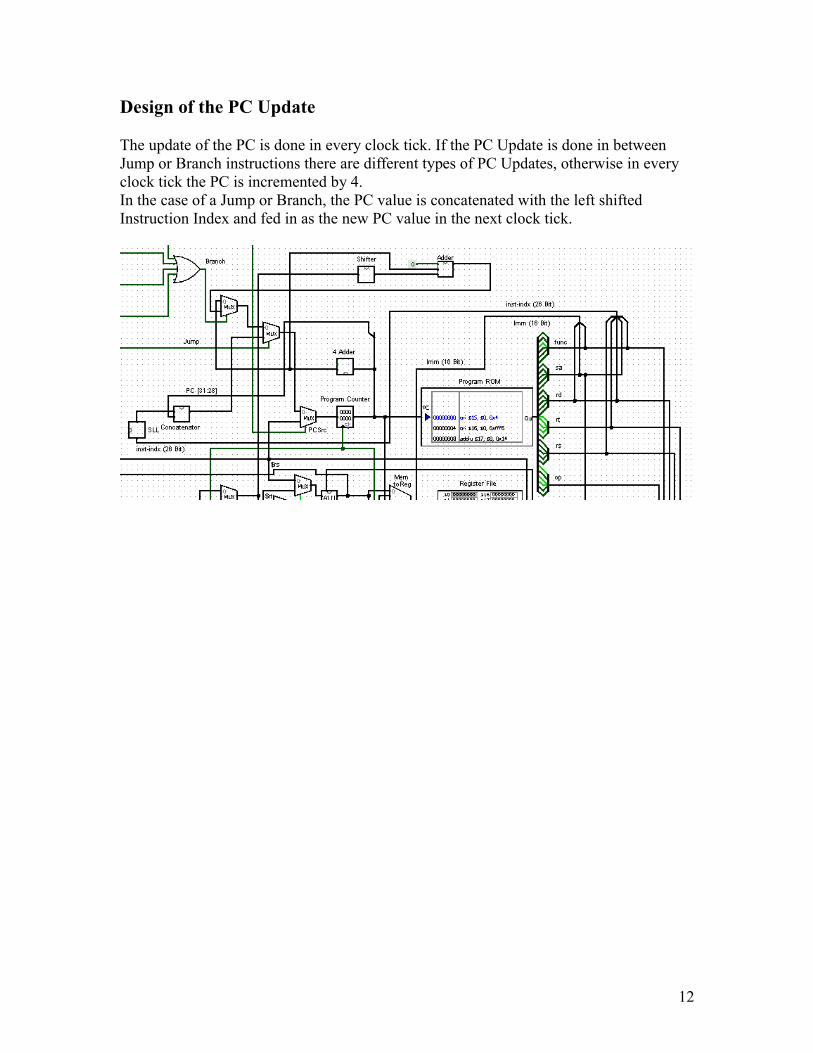
Design of the PC Update
The update of the PC is done in every clock tick. If the PC Update is done in between Jump or Branch instructions there are different types of PC Updates, otherwise in every clock tick the PC is incremented by 4. In the case of a Jump or Branch, the PC value is concatenated with the left shifted Instruction Index and fed in as the new PC value in the next clock tick.
12

Design Details for the Main Control Unit
The instruction decoding is done in the Control Units. There are two Control Units; in the first one the opcode is translated into control data. These data control the inputs to multiplexers, Register File, Memory Unit, Program Counter and the other Control Unit which controls the ALU operations.
13

Design Details for the ALU Control Unit
The ALU Control Unit controls the ALU operations to be operated by the ALU. For creating the ALU opcode the ALU Control Unit uses the opcode and function from the 32-bit address and the ALUop created by the Main Control Unit.
14

Design Details for Memory Operations
LW (Load Word)
Load 32-bit quantity from address into register rt.opcode = 0x23ALUop Addition
SW (Store Word)
Opcode = 0x2bStore Word from rt to address in memory.ALUop Addition
LUI (Load Upper Immediate)
Opcode = 15The imm value is shifted left 16-bits and stored in the register:
$t = (imm<<16); advance_pc(4)(1011 1101 1111 0111) (1011 1101 1111 0111 0000 0000 0000 0000)
ALUop nop = 000
The memory operations are controlled with the memory-related outputs of the Control Units. When the LW, SW and LUI opcodes are fed in the Control Unit the outputs are as shown in the following table:
LW SW LUIregDest 1 1 1MemRead 1 0 0MemtoReg 1 1 0ALUop 001 001 000MemWrite 0 1 0ALUSrc 1 1 1RegWrite 1 0 1
15

The memory operations are basically done in the following part of the design. In this section the input data and address is fed in the Memory Unit and the output data is sent out as follows.
Design Details for Load Upper Immediate
For the LUI instruction a concatenation operation is needed. The 16-bit Immediate read into the LUI is concatenated with 16-bit zeros as seen below:
16

Design Details for Branch Operations
The registers used for decision making, the opcode and the ALUop for controlling the ALU and other elements used for the Branch operations are listed below.
BEQ (Branch Equal to)
Opcode = 4If rs = rt increase the PC as offsetALUop Subtraction
BNE (Branch not Equal to)
Opcode = 5If rs ≠ rt increment the PCALUop Subtraction
BLTZ (Brnach Less Than Zero)
Opcode = 6If rs = 0 Branch to offsetALUop nop = 000
BGTZ (Branch Greater Than Zero)
Opcode = 7If rs ≠ 0 increment the PCALUop nop = 000
17

In the Branch Detection Units, a Zero detector is used to compare the Source Registers; the zero detector controls the difference between the Source Registers. The Zero Detector is constructed as follows.
Zero Detector
The internal designs of the Branch Control Units are visualized below:
BNE
18

BEQ
BLEZ
BGTZ
19

Source and Destination Registers of Instructions
Immediate Ops Source Reg Destination Reg regDst NotesADDI rs rt 1 +immANDI rs rt 1 +immORI rs rt 1 +immXORI rs rt 1 +imm
Memory Ops Base Reg Destination Reg Source Reg NotesLW rs rt -- regDst = 1SW rs -- rt
ALU Ops Source1 Reg Source2 Reg Destination Reg RegDstADD rs rt rd 0SUB rs rt rd 0AND rs rt rd 0OR rs rt rd 0XOR rs rt rd 0
Shift Ops Source Reg Destination Reg Shift Reg NotesSLL rt rd shamtSRL rt rd shamtSRA rt rd shamt
Shift-Mem Ops Source Reg Destination Reg Shift Reg NotesSLLV rt rd rsSRLV rt rd rs
Branch Ops Source1 Reg Source2 Reg NotesBLEZ rs -- +immBGTZ rs -- +immBEQ rs rt +immBNE rs rt +imm
20

An Interesting Detail about the Design
The number of gates used in the design is about 877 so far. ALU = 23 + AND (32) + OR (32) + XOR (32) + NOR (32) + ADDER (160) + SHIFTER (162) = 473OTHERS (including branches, concatenates, adders,..) = 366
CONTROL UNIT = 25ALU CONTROL UNIT = 13
ZERO = 5BNE = 6BEQ = 6BLEZ = 7BGTZ = 7ADDER = 160
TOTAL = 877
21

4. Implementation
We have fully implemented and tested our CPU in Logisim. The test program that we’ve used can be found in the Appendixes. It is basically constructed to realize a set of operations and it was tested if these operations were executed in the way they were expected. The result was as expected. In the following screenshots how memory and register keeps the values and how the data flow happens can be seen.
22

Also an original .c code was compiled into .s format and only the so far implemented parts (others being commented out) was tested. To be able to run the by linux compiled original code the following changes were made on the .s file:
All frame pointer addresses $fp were changed with $30.All stack pointer addresses $sp were changed with $29.The pseudo instruction li was changed with the lui and ori combination as follows:
li $4,10 lui $4,0 ; ori $4,$4,10 The move instruction was changed with the ori instructions as follows:
move $29,$30 ori $29,$29,0 ; ori $29,$30,0nop operations were changed with MIPS’s real nop instruction “sll $0,$0,0”:
nop sll $0,$0,0Syscall instructions were commented out.Jump instructions to a register like “j $31” were changed to Jump to Register instructions:
j $31 jr $31
When the above changes are made the CPU that we’ve designed works with the by linux compiled original .s file. In the following screenshots the incrementing behavior of register 2 and how register 29 keeps the address can be seen.
23

Both of the above mentioned programs can be found in the Appendix section.
24

5. Sources and References
∆ http://dropzone.tamu.edu/~wshi/350/singlecycle.ppt
∆ http://www.mips.com/
∆ http://www.amslink.com/file/rdmpback.html
∆ http://www.economicexpert.com/a/MIPS:architecture.htm
∆ http://www.seas.upenn.edu/~blundell/mipscompiler.pdf
∆ http://pages.cs.wisc.edu/~larus/spim.html
∆ http://gcc.gnu.org/onlinedocs/gcc-4.1.2/gcc/MIPS-Options.html
∆ Computer Organization & Design, 3rd Edition• By D. Patterson & J. Hennessy
25

6. Appendix
Sample Program# This program tests the following instructions:# J, JR# BEQ, BNE, BLEZ, BGTZ# LW, SW# LUI# ADDIU, ANDI, ORI, XORI# ADDU, SUBU, AND, OR, XOR, NOR# SLL, SRL, SRA, SLLV, SRLV, SRAV
# In the beginning of the program# values are loaded to some registers# to be able to do operations with them# then they are stored, loaded, added, subtracted, shifted..# In between these operations there are branches and jumps# These branches and Jumps control the path# The program terminates by itself when it at last jumps to# EXIT Label.
ORI $15, $0, 4ORI $16, $0, -10ADDIU $17, $0, 20SLL $15, $16, 4SRA $17, $15, 4SRL $16, $17, 4ADDIU $18, $0, 46797ADDIU $19, $0, 59020ORI $20, $0, 65213ORI $21, $0, 43689ORI $22, $0, 57327ADDIU $23, $0, 5319ADDIU $24, $0, 43921ADDIU $25, $0, 0ADDIU $26, $0, 4LUI $27, 1LUI $28, 10LUI $29, 1966LUI $30, 1966ORI $31, $0, 236LUI $11, 2LUI $12, 10ORI $13, $0, 100ORI $14, $0, 4SLLV $11, $12, $14SRAV $11, $13, $14SRLV $11, $13, $12
SW $29, 16($25)LW $10, 12($26)
26

ORI $12, $28, 56ORI $13, $29, 52ORI $14, $30, 46797
LOGIC1:AND $1, $20, $22OR $2, $21, $23XOR $3, $24, $25NOR $4, $26, $27BEQ $29, $30, ARITH1
J EXIT
ORI $12, $0, 0ORI $13, $0, 0ORI $14, $0, 0ORI $15, $0, 0ORI $18, $0, 0ORI $19, $0, 0ORI $20, $0, 0ORI $21, $0, 0ORI $22, $0, 0ORI $23, $0, 0
JR $16
ARITH1:ADDU $5, $28, $29SUBU $6, $30, $31ADDU $7, $18, $31SUBU $8, $19, $29
BNE $29, $30, ARITH2
ORI $29, $0, -4
BLEZ $29, ARITH2
ORI $16, $0, 0ORI $23, $0, 0ORI $24, $0, 0ORI $25, $0, 0ORI $26, $0, 0
BLEZ $25, ARITH2
ORI $27, $0, 0ORI $28, $0, 0ORI $29, $0, 0ORI $30, $0, 0ORI $31, $0, 0
JR $17
27
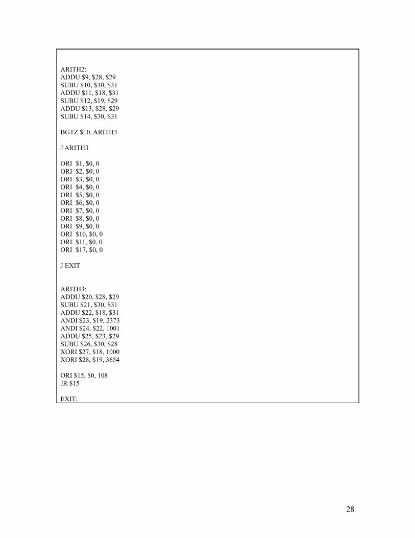
ARITH2:ADDU $9, $28, $29SUBU $10, $30, $31ADDU $11, $18, $31SUBU $12, $19, $29ADDU $13, $28, $29SUBU $14, $30, $31
BGTZ $10, ARITH3
J ARITH3
ORI $1, $0, 0ORI $2, $0, 0ORI $3, $0, 0ORI $4, $0, 0ORI $5, $0, 0ORI $6, $0, 0ORI $7, $0, 0ORI $8, $0, 0ORI $9, $0, 0ORI $10, $0, 0ORI $11, $0, 0ORI $17, $0, 0
J EXIT
ARITH3:ADDU $20, $28, $29SUBU $21, $30, $31ADDU $22, $18, $31ANDI $23, $19, 2373ANDI $24, $22, 1001ADDU $25, $23, $29SUBU $26, $30, $28XORI $27, $18, 1000XORI $28, $19, 3654
ORI $15, $0, 108JR $15
EXIT:
28

Linux Compiled C Program.c .s
#include "test-include.h"
start() { int i;
for(i = 0; i < 5; ++i) {printi(i);putc('\n');
}}
.file 1 "test2.c"
.section .mdebug.abi32
.previous
.text
.align 2
.globl printi
.ent printi
.type printi, @functionprinti:
.frame $30,8,$31 # vars= 0, regs= 1/0, args= 0, gp= 0
.mask 0x40000000,-8
.fmask 0x00000000,0addiu $29,$29,-8sw $30,0($29)ori $30,$30,0ori $30,$29,0sw $4,8($30)
#APPaddiu $2, $0, 1#syscall
#NO_APPori $29,$29,0ori $29,$30,0lw $30,0($29)addiu $29,$29,8jr $31.end printi.align 2.globl prints.ent prints.type prints, @function
prints:.frame $30,8,$31 # vars= 0, regs= 1/0, args= 0, gp= 0.mask 0x40000000,-8.fmask 0x00000000,0addiu $29,$29,-8sw $30,0($29)ori $30,$30,0ori $30,$29,0sw $4,8($30)
#APPaddiu $2, $0, 2#syscall
#NO_APP#move $29,$30lw $30,0($29)addiu $29,$29,8jr $31.end prints.align 2.globl putc.ent putc
29

.type putc, @functionputc:
.frame $30,8,$31 # vars= 0, regs= 1/0, args= 0, gp= 0
.mask 0x40000000,-8
.fmask 0x00000000,0addiu $29,$29,-8sw $30,0($29)ori $30,$30,0ori $30,$29,0ori $2,$2,0ori $2,$4,0sw $2,8($30)
#APPaddiu $2, $0, 3#syscall
#NO_APPori $29,$29,0ori $29,$30,0lw $30,0($29)addiu $29,$29,8jr $31.end putc.align 2.globl getc.ent getc.type getc, @function
getc:.frame $30,8,$31 # vars= 0, regs= 1/0, args= 0, gp= 0.mask 0x40000000,-8.fmask 0x00000000,0addiu $29,$29,-8sw $30,0($29)ori $30,$30,0ori $30,$29,0
#APPaddiu $2, $0, 4#syscall
#NO_APPori $29,$29,0ori $29,$30,0lw $30,0($29)addiu $29,$29,8jr $31.end getc.align 2.globl start.ent start.type start, @function
start:.frame $30,32,$31 # vars= 8, regs= 2/0, args= 16, gp= 0.mask 0xc0000000,-4.fmask 0x00000000,0.set noreorder.set nomacro
30
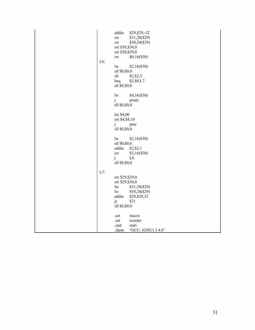
addiu $29,$29,-32sw $31,28($29)sw $30,24($29)ori $30,$30,0ori $30,$29,0sw $0,16($30)
L6:lw $2,16($30)sll $0,$0,0sll $2,$2,5beq $2,$0,L7sll $0,$0,0
lw $4,16($30)j printisll $0,$0,0
lui $4,00ori $4,$4,10j putcsll $0,$0,0
lw $2,16($30)sll $0,$0,0addiu $2,$2,1sw $2,16($30)j L6sll $0,$0,0
L7:ori $29,$29,0ori $29,$30,0lw $31,28($29)lw $30,24($29)addiu $29,$29,32jr $31sll $0,$0,0
.set macro
.set reorder
.end start
.ident "GCC: (GNU) 3.4.6"
31

7. Notes
Rapor; kaynaklar, CPU elemanları ve operasyonların İngilizce olması nedeni ile İngilizce hazırlanmıştır. İstek üzerine Türkçe olarak da hazırlanabilir.
32