journal of crystal growth - the university of virginia · abstract the low-temperature ... journal...
TRANSCRIPT

ARTICLE IN PRESS
Journal of Crystal Growth 311 (2009) 3195–3203
Contents lists available at ScienceDirect
Journal of Crystal Growth
0022-02
doi:10.1
�Corr
E-m
journal homepage: www.elsevier.com/locate/jcrysgro
Atomistic examinations of the solid-phase epitaxial growth of silicon
B.A. Gillespie �, H.N.G. Wadley
Department of Materials Science and Engineering, Wilsdorf Hall, University of Virginia, P.O. Box 400237, Charlottesville, VA 22904, USA
a r t i c l e i n f o
Article history:
Received 3 November 2008
Received in revised form
6 January 2009
Accepted 27 February 2009
Communicated by D.W. Shawfilm. The initial stages of the transformation are investigated here using a molecular dynamics
Available online 17 March 2009
PACS:
81.15.Np
87.15.ap
61.72.uf
81.10.Jt
61.43.Dq
Keywords:
A1. Computer simulation
A1. Recrystallization
A3. Solid-phase epitaxy
48/$ - see front matter & 2009 Elsevier B.V. A
016/j.jcrysgro.2009.02.050
esponding author.
ail address: [email protected] (B.A. Gillesp
a b s t r a c t
The low-temperature vapor deposition of silicon thin films and the ion implantation of silicon can result
in the formation of amorphous silicon layers on a crystalline silicon substrate. These amorphous layers
can be crystallized by a thermally activated solid-phase epitaxial (SPE) growth process. The
transformations are rapid and initiate at the buried amorphous to crystalline interface within the
simulation approach based upon a recently proposed bond order potential for silicon. The method is
used first to predict an amorphous structure for a rapidly cooled silicon melt. The radial distribution
function of this structure is shown to be similar to that observed experimentally. Molecular dynamics
simulations of its subsequent crystallization indicate that the early stage, rate limiting mechanism
appears to be removal of tetrahedrally coordinated interstitial defects in the nominally crystalline
region just behind the advancing amorphous to crystalline transition front. The activation barriers for
this interstitials migration within the bulk crystal lattice are calculated and are found to be comparable
to the activation energy of the overall solid-phase epitaxial growth process simulated here.
& 2009 Elsevier B.V. All rights reserved.
1. Introduction
The synthesis of epitaxial silicon thin films by the low-temperature condensation of its vapor to form an amorphousfilm followed by annealing to create a crystalline structure iswidely utilized during microelectronic device fabrication [1,2].Amorphous layers can also be formed during ion implantation ofcrystalline silicon, and these are also recrystallized by thermaltreatments [3]. This solid-phase epitaxial growth (SPEG) processproceeds by the thermally induced epitaxial growth of a crystalseed into the metastable amorphous region [2]. The need tocontrol point defect populations, dislocation types and densities,and stacking fault concentrations in films grown by theseprocesses has stimulated significant interest in the mechanismsof atomic reassembly at the epitaxial interface.
Thermal annealing experiments indicate the growth rate of thecrystalline phase into an amorphous silicon system obeys Arrheniuskinetics with single activation energy of 2.7 eV. This is thought toresult from a (unspecified) defect formation energy of 2.4 eV and adefect migration energy of 0.4 eV [2]. These experimental studies alsoindicate that the transformations rates can be rapid. For example, a2500-A-thick a-Si film transforms fully to a crystalline structure in
ll rights reserved.
ie).
2.5 s at a temperature of 725 1C (a growth rate of 0.1mm/s) [2]. TheSPEG rate can be affected by self-ion bombardment of the films [2].The ion bombardment of amorphous films results in a lowering of theactivation energy for the SPEG process to 0.18–0.4 eV [4,5]. Bernsteinet al. argue that this low activation energy results from the ion impactassisted formation of the rate limiting defects. The transformationfrom the amorphous to crystalline state of the ion irradiated structureis then only controlled by the migration of these defects with anactivation energy in the 0.4 eV range [6].
A detailed understanding of the atomistic mechanisms in-volved in SPEG has been impeded by the difficulties of high-resolution imaging of the moving (sometimes very rapidly) buriedinterface [7]. Computational modeling has therefore been used toinvestigate the SPEG process [6–12]. The use of computationalmodeling techniques is restricted by the relatively large numberof atoms (of order 103) that must be used to characterize eachphase [6]. Additionally these systems need to be simulated for anextended time (41 ns) to observe even the initial movement ofthe a–c interface [6]. The use of high fidelity, unbiased parameter-free quantum mechanical calculations such as density functionaltheory (DFT), is therefore prohibited [7]. A molecular dynamics(MD) approach appears the most promising, provided it employsan interatomic potential that adequately captures the radial andangular dependences of the interatomic interactions.
A computational study by Motooka et al. employing on theorder of 1000 atoms over a nanosecond timescale and utilizing the

ARTICLE IN PRESS
B.A. Gillespie, H.N.G. Wadley / Journal of Crystal Growth 311 (2009) 3195–32033196
Tersoff potential [13] found two temperature driven growthregimes in contrast to the single, experimentally observedtemperature dependency [7]. Their MD results indicated that atlow temperature, SPEG proceeded via a 2-D planar growthmechanism with an activation energy of 2.6 eV. At highertemperatures however, {111} facets were formed at the interfaceand the activation energy for growth decreased to 1.2 eV.Bernstein et al. also identified two temperature driven growthregimes in a study employing an environmentally dependentinteratomic potential (EDIP) [6,14]. However, they report anactivation energy of only 0.470.2 eV at low temperature and anenergy of 2.070.5 eV in the high-temperature regime.These activation energies are clearly in conflict with the Tersoffpotential predictions. While both studies argue that removal oflattice defects at the a–c interface is rate limiting, the defectwhose migration controls the transformation rate remainedunclear.
The most recent computational studies of SPEG performed byGarter and Weber [10–13] have employed both the Tersoff and theStillinger–Weber potential [8–12,15,16]. They examined themorphology of the a–c interface and observed that the interfaceis not sharp, but rather extends over a 6–8 atomic monolayer thickregion. They argue that the rearrangement of atomic defects in thetransition region is the limiting atomic mechanism in SPEG. Theyalso show that the concentration of the defects predicted by theTersoff potential is about double that predicted by the Stillin-ger–Weber approach [16]. It appears that the details of the atomicreassembly process observed in these studies are affected by thepotential that is used for the simulation.
Here, we use a recently developed bond order potential (BOP)for silicon and a molecular dynamics simulation method toexamine the initial stages of the amorphous to crystallinetransformation of silicon [17–21]. The BOP is an analytic, many-body interatomic potential derived by coarse graining theelectronic structure within a two-center, tight-binding represen-tation of covalent bonding. This results in an interatomic potentialthat explicitly accounts for both the s and p bonding componentsof covalent bonding. It also explicitly includes a term to accountfor the promotion energy associated with the hybridization of theatomic orbitals. While the BOP approach to molecular dynamicssimulations is more computationally demanding than many otherpotentials, the use of this potential here is motivated by the highquality of its predictive results for silicon bulk properties (such asmelting temperature and the cohesive energies of a wide range ofstructures) and its reasonable estimates for point defect energiesand structures [17].
Computational resource limitations constrain our simulationswith this BOP approach to systems of 1000 atoms and for shorttimes (�1 ns). As a result, the simulation is capable of onlyresolving the initial atomic reassembly processes. We note at theoutset that the initial growth rates observed below and inprevious studies of the simulations of the SPEG process in siliconare several orders of magnitude faster than that observedexperimentally [6–12]. We suspect there exist a SPEG mechanismthat is activated after the initial stage examination is complete.The discovery of its mechanism awaits much larger timescale MDsimulations.
The atomic scale structure of the amorphous films createdusing the BOP have been examined, and are found to contain ahigh concentration of both 3 and 5 coordinated atoms. Thisindicates that the BOP predicts a highly defected amorphous filmsimilar to that observed in ion-implanted films. These defectsresult in fast diffusion pathways and a correlation is drawnbetween removal of interstitial defects at the a–c interface andrapid epitaxial growth. The BOP-based simulations are thenemployed to investigate the activation energy barriers to the
migration of interstitial defects within the bulk. These energybarriers are observed to be similar to the calculated overallactivation energy for solid-phase epitaxial growth process.
2. Simulation details
A complete description of the development of the bond orderpotential can be found in Refs. [17–21]. There are numerous waysto synthesize amorphous silicon including quenching from themelt [22], low-temperature vapor deposition [23–25], and ionbombardment [26,27]. The a-Si films generated by each methodhave different atomic scale structures [2]. Amorphous silicongenerated by rapidly cooling the liquid phase results in theformation of a network of tetrahedrally coordinated atoms withno long-range order (an ‘‘ideal’’ amorphous film) [22]. Low-temperature vapor deposited films are amorphous, but alsosometimes contain low-density regions and voids [2]. These area consequence of self-shadowing during the deposition processcombined with low atom mobility on the film surface [2]. Whenthe deposited atoms are unable to significantly migrate across thesurface, the atoms assemble into a random network with no long-range periodicity. Ion implantation causes atoms to be displacedfrom their lattice sites by primary and secondary collisionprocesses [2]. Continuous ion bombardment results in the overlapof the damage zone of individual impacts eventually leading to afully amorphous structure. Amorphous silicon films created by ionbombardment contain a large concentration of three- and five-fold bonding defects [28].
To prepare a computational amorphous/crystalline (a–c) inter-face a 23.0375 A [10 1] by 43.44 A [0 10] by 23.0375 A [10 1]volume single crystal was created. This crystal was made up of1152 atoms distributed in 32 (0 10) layers. Periodic boundaryconditions were employed in the [10 1] and [10 1] directions. Thetop 24 monolayers were then melted elevating their temperatureto 2000 K for 50 ps (for 25,000 time steps with a time step,Dt=2 fs), while the bottom 8 monolayers were thermally con-strained to 500 K with the lowest two layers rigidly fixed in space.This resulted in a thin crystalline substrate with a layer of liquidsilicon on top. This system was then quenched to the desiredtemperature over a period of 50 ps to create a computationalsample containing a region of crystalline and amorphous materialseparated by an amorphous to crystalline interface. This systemwas then thermally annealed for 5 ns and the resulting epitaxialgrowth rate and rate limiting defect migration energy barriers areinvestigated.
The epitaxial growth rate was measured by tracking the rate ofchange of the number of crystalline atoms present in the systemby identifying the bonding environment of an atom and that of itsneighbors. In order for an atom to be classified as part of acrystalline region it was required to maintain, within a toleranceof 101, the 1091 tetrahedral arrangement of its bonds with its fournearest neighbors. The increase in the number of atoms thatsatisfied this condition gave the epitaxial growth rate in atoms perunit time interval.
The interstitials present in the crystallized region were alsoidentified and their diffusion pathways were examinedusing molecular statics techniques [29]. Starting from agiven interstitial configuration, the interstitial atom was incre-mentally moved in the direction of minimum energy alonga path to another interstitial position. After each incrementalmovement, the entire system was allowed to relax in energyaround the constrained interstitial atom. This then allowedthe energy along the migration path to be computed and theenergy barrier to interstitial migration within the crystal to bedetermined.

ARTICLE IN PRESS
B.A. Gillespie, H.N.G. Wadley / Journal of Crystal Growth 311 (2009) 3195–3203 3197
3. The amorphous structure
The radial distribution function (RDF) for the a-Si filmproduced by the rapid solidification simulation is shown inFig. 1. The simplest view of amorphous silicon is that of acontinuous random network of tetrahedrally coordinated atoms[2]. Therefore one would expect that the RDF of an amorphousstructure will display a large slender peak centered near the bulksilicon equilibrium nearest neighbor distance, followed bybroadened secondary and tertiary peaks. The RDF obtained byanalyzing the quenched structure generally agrees with thisinterpretation. The data obtained from the simulation also agreewell with that deduced by experiment [30].
Many of the other interatomic potentials poorly predict therandom tetrahedral network of a-Si, predicting a large number of3 and 5 coordinated atoms [31]. The inset in Fig. 1 shows thedistribution of atomic coordinations in the amorphous regionpredicted by the BOP analysis. The BOP predicts a broaddistribution of atomic coordination’s with a maximum at 4 andan average of 4.16. While amorphous silicon films are usuallyconsidered a uniform random network of coordination 4 atoms, inpractice the various experimental methods for generating amor-phous thin films result in slightly different amorphous states [2].It should also be noted that the quenching rate plays a significantrole in the a-Si structure. For example, the amorphous filmgenerated by ion implantation techniques contains many atomsthat are not four-fold coordinated [2]. Spectroscopic studies ofself-implanted a-Si have shown a large concentration of danglingbonds associated with three-fold coordinated atoms and floatingbonds resulting from five-fold coordinated atoms [28]. Thesignificant fraction of atoms that do not have four-fold coordina-tion suggest the amorphous region of the BOP simulation is highlydefected. This high concentration of defects suggests that the(very rapidly cooled) simulated structure is similar to that ionbeam irradiated structures where defects are introduced to thesystem by a non-thermal ion collision process.
Fig. 1. Radial distribution function g(r) for a-Si compared to experimental a-Si
data. Inset: the atomic coordination distribution of silicon atoms in the a-Si region
graphed as a percentage of frequency as predicted by simulation.
4. Epitaxial crystallization
The quenched computational system was annealed at numer-ous temperatures between 700 and 950 K and the growth rate ofthe a–c interface during the SPEG process was determined. This isplotted as a function of inverse absolute temperature in Fig. 2. Thegrowth rate data are reasonably well fitted by an Arrheniusrelation with an activation energy barrier of 0.87 eV. Thisactivation energy is about twice that experimentally reportedfor ion beam irradiated silicon [5]. Earlier simulation studies havereported a wide range of activation energies [6–12], and it shouldbe noted that the activation barrier obtained here is comparable tothat observed in simulations employing the Stillinger–Weberpotential and a similar MD cell [12]. Using their environmentallydependent modeling approach, Bernstein et al. [6] have shownthat the low-temperature activation barrier (0.2 eV) observed intheir simulations corresponds to the migration of defects whilethe larger value (2.0 eV) seen at higher temperatures correspondsto a more complicated process involving defect formation anddiffusion. The a-Si film formed by very rapidly quenching the Si-BOP structure contained a large concentration of ‘‘frozen in’’defects and we suspect this is responsible for our observation ofan activation barrier lying between those of the Bernstein et al.limits.
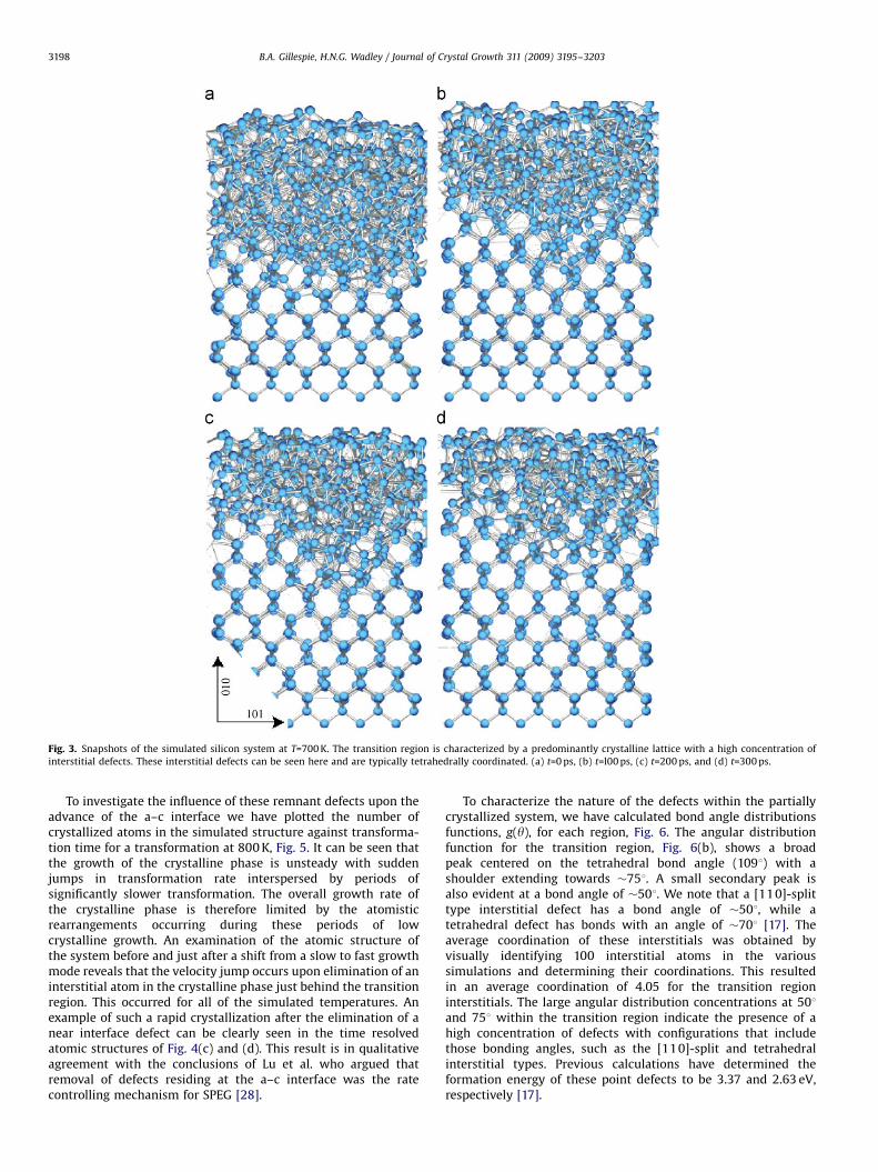
To investigate the atomic scale details of the a–c transforma-tion, time resolved atomic structures near the a–c interface forannealing temperatures of 700 and 900 K are presented in Figs. 3and 4. They show the advancing amorphous to crystalline frontmoving through the amorphous region. It can be seen that themost recently crystallized region in each time resolved viewconsists of a predominantly crystalline lattice containing a highconcentration of interstitial defects. Detailed examination of thetransition region indicates that overlap of the lattice strains ofthese interstitial defects eventually gives rise to the continuousrandom network of the a-Si layer as one move upwards throughthe simulated region.
Fig. 2. Dependence of the SPE growth rate on simulated temperature.
ARTICLE IN PRESS
Fig. 3. Snapshots of the simulated silicon system at T=700 K. The transition region is characterized by a predominantly crystalline lattice with a high concentration of
interstitial defects. These interstitial defects can be seen here and are typically tetrahedrally coordinated. (a) t=0 ps, (b) t=l00 ps, (c) t=200 ps, and (d) t=300 ps.
B.A. Gillespie, H.N.G. Wadley / Journal of Crystal Growth 311 (2009) 3195–32033198
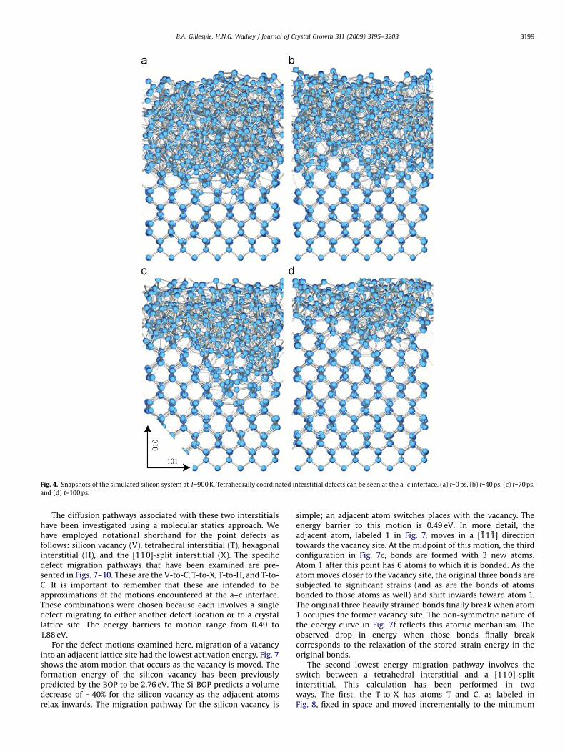
To investigate the influence of these remnant defects upon theadvance of the a–c interface we have plotted the number ofcrystallized atoms in the simulated structure against transforma-tion time for a transformation at 800 K, Fig. 5. It can be seen thatthe growth of the crystalline phase is unsteady with suddenjumps in transformation rate interspersed by periods ofsignificantly slower transformation. The overall growth rate ofthe crystalline phase is therefore limited by the atomisticrearrangements occurring during these periods of lowcrystalline growth. An examination of the atomic structure ofthe system before and just after a shift from a slow to fast growthmode reveals that the velocity jump occurs upon elimination of aninterstitial atom in the crystalline phase just behind the transitionregion. This occurred for all of the simulated temperatures. Anexample of such a rapid crystallization after the elimination of anear interface defect can be clearly seen in the time resolvedatomic structures of Fig. 4(c) and (d). This result is in qualitativeagreement with the conclusions of Lu et al. who argued thatremoval of defects residing at the a–c interface was the ratecontrolling mechanism for SPEG [28].
To characterize the nature of the defects within the partiallycrystallized system, we have calculated bond angle distributionsfunctions, g(y), for each region, Fig. 6. The angular distributionfunction for the transition region, Fig. 6(b), shows a broadpeak centered on the tetrahedral bond angle (1091) with ashoulder extending towards �751. A small secondary peak isalso evident at a bond angle of �501. We note that a [110]-splittype interstitial defect has a bond angle of �501, while atetrahedral defect has bonds with an angle of �701 [17]. Theaverage coordination of these interstitials was obtained byvisually identifying 100 interstitial atoms in the varioussimulations and determining their coordinations. This resultedin an average coordination of 4.05 for the transition regioninterstitials. The large angular distribution concentrations at 501and 751 within the transition region indicate the presence of ahigh concentration of defects with configurations that includethose bonding angles, such as the [110]-split and tetrahedralinterstitial types. Previous calculations have determined theformation energy of these point defects to be 3.37 and 2.63 eV,respectively [17].
ARTICLE IN PRESS
Fig. 4. Snapshots of the simulated silicon system at T=900 K. Tetrahedrally coordinated interstitial defects can be seen at the a–c interface. (a) t=0 ps, (b) t=40 ps, (c) t=70 ps,
and (d) t=100 ps.
B.A. Gillespie, H.N.G. Wadley / Journal of Crystal Growth 311 (2009) 3195–3203 3199
The diffusion pathways associated with these two interstitialshave been investigated using a molecular statics approach. Wehave employed notational shorthand for the point defects asfollows: silicon vacancy (V), tetrahedral interstitial (T), hexagonalinterstitial (H), and the [110]-split interstitial (X). The specificdefect migration pathways that have been examined are pre-sented in Figs. 7–10. These are the V-to-C, T-to-X, T-to-H, and T-to-C. It is important to remember that these are intended to beapproximations of the motions encountered at the a–c interface.These combinations were chosen because each involves a singledefect migrating to either another defect location or to a crystallattice site. The energy barriers to motion range from 0.49 to1.88 eV.
For the defect motions examined here, migration of a vacancyinto an adjacent lattice site had the lowest activation energy. Fig. 7shows the atom motion that occurs as the vacancy is moved. Theformation energy of the silicon vacancy has been previouslypredicted by the BOP to be 2.76 eV. The Si-BOP predicts a volumedecrease of �40% for the silicon vacancy as the adjacent atomsrelax inwards. The migration pathway for the silicon vacancy is
simple; an adjacent atom switches places with the vacancy. Theenergy barrier to this motion is 0.49 eV. In more detail, theadjacent atom, labeled 1 in Fig. 7, moves in a [111] directiontowards the vacancy site. At the midpoint of this motion, the thirdconfiguration in Fig. 7c, bonds are formed with 3 new atoms.Atom 1 after this point has 6 atoms to which it is bonded. As theatom moves closer to the vacancy site, the original three bonds aresubjected to significant strains (and as are the bonds of atomsbonded to those atoms as well) and shift inwards toward atom 1.The original three heavily strained bonds finally break when atom1 occupies the former vacancy site. The non-symmetric nature ofthe energy curve in Fig. 7f reflects this atomic mechanism. Theobserved drop in energy when those bonds finally breakcorresponds to the relaxation of the stored strain energy in theoriginal bonds.
The second lowest energy migration pathway involves theswitch between a tetrahedral interstitial and a [110]-splitinterstitial. This calculation has been performed in twoways. The first, the T-to-X has atoms T and C, as labeled inFig. 8, fixed in space and moved incrementally to the minimum

ARTICLE IN PRESS
Fig. 5. A small excerpt in time showing the thermally driven epitaxial growth of
silicon crystal. The dashed lines highlight the change in growth rate, and can be
used to isolate the rate limiting atomic mechanism to the growth. The solid line
indicates the overall growth rate.
Fig. 6. Distribution of bond angles in the crystalline region (a), the transition
region (b) and the amorphous region (c).
B.A. Gillespie, H.N.G. Wadley / Journal of Crystal Growth 311 (2009) 3195–32033200
energy configuration of the X interstitial. The second method, theX-to-C, has atom X1, as labeled in Fig. 8, fixed in space andincrementally moved into its associated lattice site; atom X2 isallowed to move freely and as a result minimizes into atetrahedral site. In both of these methods all other atoms areallowed to reach their minimum energy configuration at eachincrement. Both methods simulate the motion between a T and Xinterstitial configuration. The energy barrier to this migration is0.75–0.97 eV. Fig. 8 shows the high energy configuration for thisatomic motion. Significant lattice distortions occur in theneighboring atoms. Because of the very small energy barrier tomigration in the X-to-T direction (0.14 eV) it is unlikely that X typeinterstitials will have a long lifespan in simulation.
The third defect migration of interest is the migration of aninterstitial from one tetrahedral site to another tetrahedral site. Itshould be noted that the midpoint between any two tetrahedralsites is a hexagonal site. Therefore, by symmetry, the energetic ofthe migration can be fully considered by examining the T-to-Hpathway as shown in Fig. 9. The hexagonal interstitial is predictedby the Si-BOP to be metastable with an energy of formation of3.85 eV [17]. Any small thermally induced distortion from perfectsymmetry will result in the hexagonally coordinated interstitialdefect transitioning into a tetrahedral site. As a result the energybarrier to migration from one tetrahedral site to another isapproximately the same as the difference between their formationenergies, 1.10 eV.
The final and highest energy defect migration examined is for atetrahedral coordinated atom to directly displace a neighboringlattice site atom. This atomic motion is labeled T-to-C. Thetetrahedral interstitial atom is incrementally moved towards aneighboring lattice atom site. This pushes the crystalline atom outof its lattice site towards a nearby low energy tetrahedral site (notthe same tetrahedral site that is already occupied). The highenergy configuration of this motion is shown in Fig. 10.Considerable lattice distortion is encountered in this motion dueto the motion requiring the breaking and reforming of 6 strongatomic bonds. This atomistic mechanism encounters an energybarrier of 1.88 eV, considerably higher than any of the othermotions examined.
The above analysis indicates several possible pathwaysfor a tetrahedral interstitial to migrate to a nearby tetrahedral
interstitial site. The tetrahedral interstitial atom could directlydisplace an adjacent crystal atom, pushing that atom into a nearbytetrahedral site. This motion, the T-to-C mechanism, has beenshown to have a very large energy of activation of 1.88 eV. Anotherpath migrates the tetrahedral interstitial through a hexagonalinterstitial site. This pathway has been found to have an activation

ARTICLE IN PRESS
Fig. 7. Vacancy migration pathway in the bulk silicon lattice. (a) The initial configuration of the vacancy; the relaxation of the crystal lattice in towards the vacancy is
shown. (b)–(d) The transition configurations 2–4, respectively. (e) The final configuration, identical to the initial except the vacancy has moved to an adjacent lattice site. (f)
The energy barriers to vacancy motion.
B.A. Gillespie, H.N.G. Wadley / Journal of Crystal Growth 311 (2009) 3195–3203 3201
barrier of 1.1 eV, which is much lower than the T-to-C mechanismbut still higher than the T-to-X pathway. The lowest energypathway for tetrahedral interstitial migration is to first overcomea 0.75–0.97 eV energy barrier to form a X interstitial. This energyrange is obtained from energy differences in migrating theinterstitial atom in both directions. The X interstitial thenovercomes a 0.14 eV barrier to transform back into a T interstitialin a new tetrahedral site. Because this last motion has the lowestenergy, it is the mechanism that is most likely to occur.
5. Summary
We have studied the solid-phase epitaxial growth of siliconusing the recently developed bond order potential [17]. The solid-phase epitaxial process involves the spontaneous, thermallyactivated rearrangement of atomic bonds at the amorphous/
crystal interface [2]. For an ion-implanted amorphous surface,experimental studies have shown that this process results in themotion of a sharp a–c interface towards the free surface [2]. Thegrowth rate of the crystalline region (or the velocity of the a–cinterface) can be well modeled by an Arrhenius relation withactivation energy of 2.7 eV [2]. Ion bombardment introducesdefects into the amorphous film which enhance the growth rateand reduce the activation energy to 0.18–0.4 eV [6]. The rapidquenching from the liquid phase method used to obtain theamorphous film used in the present simulations results in a highlydefected amorphous film. As a result the a-Si found in the presentsimulations is similar to an unrelaxed amorphous film under ionbombardment. The BOP predicts activation energy of 0.87 eV forthe SPE process.
Previous atomistic modeling research has shown that defectsplay a key role in SPEG [6–12]. The exact nature of that role hasdiffered depending on which interatomic potential was employed.

ARTICLE IN PRESS
Fig. 8. Interstitial migration pathway for the T-to-X transition. Interstitial atoms are designated by hollow circles and atoms on different planes are differentiated by
differing size. The interstitial atoms move on the smaller circle atom plane. (a) The tetrahedral intersitial configuration. (b) The configuration of the highest energy. (c) The X
intersitial configuration. (d) The energy barrier to intersitial motion.
Fig. 9. Interstitial migration pathway for the T-to-H transition. The interstitial
atoms are represented by hollow circles. Atoms on different planes are of differing
sizes. (a) The tetrahedral intersitial configuration. (b) The hexagonal intersitial
configuration. (c) The energy barrier to interstitial motion.Fig. 10. Interstitial migration pathway for the T-to-C transition. Atoms in different
planes are represented by circles of differing sizes. The interstitials are shown as
open circles, (a) the tetrahedral interstitial. (b) The atomic structure at the energy
peak. (c) The new tetrahedral interstitial was formed by a lattice site atom. (d) The
energy barrier to this motion.
B.A. Gillespie, H.N.G. Wadley / Journal of Crystal Growth 311 (2009) 3195–32033202
The BOP also indicated that defect migration is an essential aspectof the atomistic mechanism that rate limits the SPE process. TheBOP-based simulations clearly indicate that the rapidly advancingcrystalline front is slowed by the need to remove trappedinterstitials at the interface. These interstitials distort thesurrounding crystal lattice and prevent further crystallizationuntil they are removed. These interstitials have been found to befour-fold coordinated, indicating that they are predominantly ofthe (110)-split (X) and tetrahedral (T) type. The bonding
environment of the transition region in which these interstitialsare found is predominantly crystalline. We therefore believe thatthe activation energy for the movement of these interstitialsthrough a crystalline lattice will be comparable to the activationenergy of their movement in the transition region. The X-to-Ttransition was found to have an energy barrier between 0.75 and

ARTICLE IN PRESS
B.A. Gillespie, H.N.G. Wadley / Journal of Crystal Growth 311 (2009) 3195–3203 3203
0.97 eV. This energy is comparable to the 0.87 eV activation energyfor SPE as predicted by the BOP. This result suggests that theannihilation of interstitial defects at the a–c interface is the ratelimiting mechanism for solid-phase epitaxial growth.
Acknowledgements
We gratefully acknowledge the support of this work by DARPAand ONR under ONR Contract no. N00014-03-C-0288. C. Schwartzand J. Christodoulou were the program managers.
References
[1] J.C. Bean, Semiconductors and Semimetals 56 (1999) 1.[2] G.L. Olson, J.A. Roth, Mater. Sci. Rep. 3 (1988) 1.[3] T. Motooka, Mater. Sci. Eng. A 253 (1998) 42.[4] F. Priolo, E. Rimini, Mater. Sci. Rep. 5 (1990) 319.[5] A. Kinomura, J.S. Williams, K. Fujii, Phys. Rev. B 59 (1999) 15214.[6] N. Bernstein, M.J. Aziz, E. Kaxiras, Phys. Rev. B 61 (2000) 6696.[7] T. Motooka, K. Nisihira, S. Munetoh, K. Moriguchi, A. Shintani, Phys. Rev. B 61
(2000) 8537.[8] B. Weber, K. Gartner, D.M. Stock, Nucl. Instrum. Meth. Phys. Res. B 127/128
(1997) 239.
[9] B. Weber, D.M. Stock, K. Gartner, Nucl. Instrum. Meth. Phys. Res. B 148 (1999)375.
[10] D.M. Stock, B. Weber, K. Gartner, Phys. Rev. B 61 (2000) 8150.[11] B. Weber, K. Gartner, Nucl. Instrum. Meth. Phys. Res. B 175 (2001) 119.[12] K. Gartner, B. Weber, Nucl. Instrum. Meth. Phys. Res. B 202 (2003) 255.[13] J. Tersoff, Phys. Rev. B 37 (1988) 6991.[14] M.Z. Bazant, E. Kaxiras, J.F. Justo, Phys. Rev. B 56 (1997) 8542.[15] F.H. Stillinger, T.A. Weber, Phys. Rev. B 31 (1985) 5262.[16] G. Otto, G. Hobler, K. Gartner, Nucl. Instrum. Meth. Phys. Res. B 202 (2003)
114.[17] B.A. Gillespie, X.W. Zhou, D.A. Murdick, H.N.G. Wadley, R. Drautz, D.G. Pettifor,
Phys. Rev. B 75 (2007) 155207.[18] D.G. Pettifor, I.I. Oleinik, Phys. Rev. B 59 (1999) 8487.[19] D.G. Pettifor, I.I. Oleinik, Phys. Rev. Lett. 84 (2000) 4124.[20] P.L. Liu, R. Yen, N. Bloembergen, R.T. Hodgson, Appl. Phys. Lett. 34 (1979) 864.[23] D.G. Pettifor, I.I. Oleinik, Phys. Rev. B 65 (2002) 172103.[21] D.G. Pettifor, I.I. Oleinik, D. Nguyen-Manh, et al., Comp. Mat. Sci. 23 (2002) 33.[22] M.H. Brodsky, R.S. Title, K. Weiser, G.D. Pettit, Phys. Rev. B 1 (1970) 2639.[24] T.I. Kemins, M.M. Mandurah, K.C. Saraswat, J. Electrochem. Soc. 125 (1978)
927.[25] J.A. Roth, C.L. Anderson, Appl. Phys. Lett. 31 (1977) 689.[26] J.W. Mayer, L. Eriksson, J.A. Davies, Ion Implantation in Semiconductors,
Academic Press, New York, 1970.[27] W.L. Brown, Mater. Res. Soc. Symp. Proc. 51 (1985) 53.[28] G.Q. Lu, E. Nygren, M.J. Aziz, J. Appl. Phys. 70 (1991) 5323.[29] X.W. Zhou, The Nitrogen Strengthening Mechanism in the Single Crystalline
Fe–Ni–Cr Austenitic Stainless Steels, Dissertation, Clemson University, 1995.[30] C.R.S. da Silva, A. Fazzio, Phys. Rev. B 64 (2001) 075301.[31] Private communication with Khristian Koharty at Oxford University (2006).