jedec standard - Микроконтроллерыcaxapa.ru/thumbs/462742/jesd78b.pdf · jedec...
TRANSCRIPT
JEDEC STANDARD IC Latch-Up Test JESD78B (Revision of JESD78A, November 2005) DECEMBER 2008 JEDEC SOLID STATE TECHNOLOGY ASSOCIATION
NOTICE
JEDEC standards and publications contain material that has been prepared, reviewed, and approved through the JEDEC Board of Directors level and subsequently reviewed and approved
by the JEDEC legal counsel.
JEDEC standards and publications are designed to serve the public interest through eliminating misunderstandings between manufacturers and purchasers, facilitating interchangeability and
improvement of products, and assisting the purchaser in selecting and obtaining with minimum delay the proper product for use by those other than JEDEC members, whether the standard is to be
used either domestically or internationally.
JEDEC standards and publications are adopted without regard to whether or not their adoption may involve patents or articles, materials, or processes. By such action JEDEC does not assume any liability to any patent owner, nor does it assume any obligation whatever to parties adopting
the JEDEC standards or publications.
The information included in JEDEC standards and publications represents a sound approach to product specification and application, principally from the solid state device manufacturer
viewpoint. Within the JEDEC organization there are procedures whereby a JEDEC standard or publication may be further processed and ultimately become an ANSI standard.
No claims to be in conformance with this standard may be made unless all requirements stated in
the standard are met.
Inquiries, comments, and suggestions relative to the content of this JEDEC standard or publication should be addressed to JEDEC at the address below, or call (703) 907-7559 or www.jedec.org
Published by
©JEDEC Solid State Technology Association 2008 3103 North 10th Street
Suite 240 South Arlington, VA 22201-2107
This document may be downloaded free of charge; however JEDEC retains the copyright on this material. By downloading this file the individual agrees not to
charge for or resell the resulting material.
PRICE: Please refer to the current Catalog of JEDEC Engineering Standards and Publications online at
http://www.jedec.org/Catalog/catalog.cfm
Printed in the U.S.A. All rights reserved
PLEASE!
DON’T VIOLATE THE
LAW!
This document is copyrighted by JEDEC and may not be reproduced without permission.
Organizations may obtain permission to reproduce a limited number of copies
through entering into a license agreement. For information, contact:
JEDEC Solid State Technology Association 3103 North 10th Street
Suite 240 South Arlington, VA 22201-2107
or call (703) 907-7559

JEDEC Standard No. 78B
-i-
IC LATCH-UP TEST
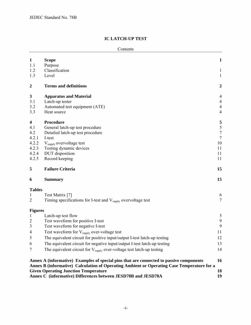
Contents
1 Scope 1 1.1 Purpose 1.2 Classification 1 1.3 Level 1 2 Terms and definitions 2 3 Apparatus and Material 4 3.1 Latch-up tester 4 3.2 Automated test equipment (ATE) 4 3.3 Heat source 4 4 Procedure 5 4.1 General latch-up test procedure 5 4.2 Detailed latch-up test procedure 7 4.2.1 I-test 7 4.2.2 Vsupply overvoltage test 10 4.2.3 Testing dynamic devices 11 4.2.4 DUT disposition 11 4.2.5 Record keeping 11 5 Failure Criteria 15 6 Summary 15 Tables 1 Test Matrix [7] 6 2 Timing specifications for I-test and Vsupply overvoltage test 7 Figures 1 Latch-up test flow 5 2 Test waveform for positive I-test 9
3 Test waveform for negative I-test 9 4 Test waveform for Vsupply over-voltage test 11 5 The equivalent circuit for positive input/output I-test latch-up testing 12 6 The equivalent circuit for negative input/output I-test latch-up testing 13 7 The equivalent circuit for Vsupply over-voltage test latch-up testing 14 Annex A (informative) Examples of special pins that are connected to passive components 16 Annex B (informative) Calculation of Operating Ambient or Operating Case Temperature for a Given Operating Junction Temperature 18 Annex C (informative) Differences between JESD78B and JESD78A 19

JEDEC Standard No. 78B
-ii-

JEDEC Standard No. 78B Page 1
IC LATCH-UP TEST (From JEDEC Board Ballot JCB-96-69 and JCB-08-45, formulated under the cognizance of JC-14.1 Committee on Reliability Test Methods for Packaged Devices.) 1 Scope This specification covers the I-test and the overvoltage latch-up testing of integrated circuits. The purpose of this specification is to establish a method for determining IC latch-up characteristics and to define latch-up failure criteria. Latch-up characteristics are extremely important in determining product reliability and minimizing No Trouble Found (NTF) and Electrical Overstress (EOS) failures due to latch-up. This test method is applicable to NMOS, CMOS, bipolar, and all variations and combinations of these technologies. 1.1 Classification There are two classes for latch-up testing. • Class I is for testing at room temperature ambient. • Class II is for testing at the maximum operating ambient temperature (Ta) or maximum operating case
temperature (Tc) or maximum operating junction temperature (Tj) in the data sheet.
For Class II testing at the maximum operating Ta or Tc, the ambient temperature or case temperature (Tc) shall be established at the required test value. For Class II testing at the maximum operating Tj, the ambient temperature Ta or the case temperature Tc should be selected to achieve a temperature characteristic of the junction temperature for a given device operating mode(s) during latch-up testing. The maximum operating ambient or case temperature during stress may be calculated based on the methods detailed in Annex B. The values used in Class II testing shall be recorded in the final report. NOTE Elevated temperature will reduce latch-up resistance, and class II testing is recommended for devices that are required to operate at elevated temperature. 1.2 Level Level defines the I-test current injection value used during latch-up testing. Latch-up passing levels are defined as follows: Level A - The trigger current value in Table 1 shall be +100 mA as defined in Figure 5 and -100 mA as defined in Figure 6. If all pins on the part pass at least the Level A trigger current values, then the part shall be considered a Level A part. Level B – If any pins on the part do not pass the Level A standard, then the supplier shall determine the minimum passing trigger current requirement for each pin stressed differently than in Level A. The maximum (or highest) passing trigger current value shall be reported in the record for each pin stressed differently than in Level A, and the part shall be considered to be a Level B part, see 4.2.5.
JEDEC Standard No. 78B Page 2
2 Terms and definitions The following terms and definitions apply to this test method. cool-down time: The period of time between successive applications of trigger pulses, or the period of time between the removal of the Vsupply voltage and the application of the next trigger pulse. (See Figures 2, 3, and 4 and Table 2.) DUT: The device under test. GND (Ground): The common or zero-potential pin(s) of the DUT. NOTE 1 Ground pins are not latch-up tested. NOTE 2 A ground pin is sometimes called Vss. input pins: All address, data-in control, Vref, and similar pins. I/O (bidirectional) pins: Device pins that can be made to operate as an input or an output or in a high-impedance state. Isupply: The total supply current in each Vsupply pin (or pin group) with the DUT biased as indicated in Table 1. I-test: A latch-up test that supplies positive and negative current pulses to the pin under test. latch-up: A state in which a low-impedance path, resulting from an overstress that triggers a parasitic thyristor structure, persists after removal or cessation of the triggering condition. NOTE 1 The overstress can be a voltage or current surge, an excessive rate of change of current or voltage, or any other abnormal condition that causes the parasitic thyristor structure to become regenerative. NOTE 2 Latch-up will not damage the device provided that the current through the low-impedance path is sufficiently limited in magnitude or duration. logic-high: A level within the more positive (less negative) of the two ranges of logic levels chosen to represent the logic states. NOTE 1 For digital devices, the maximum value of the high logic level voltage is used for latch-up testing. The maximum logic high level is designated as Vmax. NOTE 2 For non-digital devices, the maximum operating voltage that can be applied to that pin as defined in the device specification is used for latch-up testing.
JEDEC Standard No. 78B Page 3
2 Terms and definitions (cont’d) logic-low: A level within the more negative (less positive) of the two ranges of logic levels chosen to represent the logic states. NOTE 1 For digital devices, the minimum value of the low logic level voltage is used for latch-up testing. The minimum logic low level is designated as Vmin. NOTE 2 For non-digital devices, the minimum operating voltage that can be applied to that pin as defined in the device specification is used for latch-up testing. maximum Vsupply; maximum operating voltage: The maximum supply voltage at which a device is specified to operate in compliance with the applicable device specification. NOTE 1 “Maximum” refers to the magnitude of supply voltage and can be either positive or negative. NOTE 2 The maximum voltage is not the absolute maximum rated voltage, i.e., the voltage beyond which permanent damage is likely. “no connect” pin: A pin that has no internal connection and that can be used as a support for external wiring without disturbing the function of the device. NOTE All “no connect” pins shall be left in an open (floating) state during latch-up testing. nominal Isupply (Inom): The measured dc supply current for each Vsupply pin (or pin group) with the DUT biased at the test temperature as defined in clause 4 and Table 1. output pin: A device pin that generates a signal or voltage level as a normal function during the normal operation of the device. NOTE Output pins, though left in an open (floating) state during testing of other pin types, are latch-up tested. preconditioned pin: A device pin that has been placed in a defined state or condition (input, output, high impedance, etc.) by applying control vectors to the DUT. testing of dynamic devices: Latch-up trigger testing of a device in a known stable state, at the minimum-rated clock frequency applied to the device (see 4.2.3 for specified conditions). test condition: The test temperature, supply voltage, current limits, voltage limits, clock frequency, input bias voltages, and preconditioning vectors applied to the DUT during the latch-up test. timing-related input pin: A pin such as clock crystal oscillator, charge pump circuit, etc., required to place the DUT in a normal operating mode. NOTE Required timing signals may be applied by the latch-up tester, external equipment, and/or external components as appropriate. trigger pulse: The positive or negative current pulse (I-Test) or voltage pulse (Vsupply overvoltage test) applied to any pin under test in an attempt to induce latch-up (see Figures 2, 3 and 4).

JEDEC Standard No. 78B Page 4
2 Terms and definitions (cont’d) trigger duration: The duration of an applied pulse from the trigger source. (See Figures 2, 3, and 4 and Table 2.) Vsupply pin (or pin group): All DUT power supply and external voltage source pins (excluding ground pins), including both positive- and negative-potential pins. NOTE 1 Generally, it is permissible to treat equal-potential voltage source pins as one Vsupply pin (or pin group) and connect them to one power supply. NOTE 2 When forming Vsupply pins (or pin groups), the combination of Vsupply pins with significantly different supply current levels is not recommended as this would make it difficult to detect significant current changes on low supply current pins. Vsupply overvoltage test: A latch-up test that supplies overvoltage pulses to the Vsupply pin under test. 3 Apparatus and material The apparatus required for this test method includes the following: 3.1 Latch-up tester Test equipment capable of performing the tests as specified in this document. For devices requiring dynamic testing, the test equipment shall be capable of supplying timing signals and logic setup vectors required to control the I/O pin output states as specified in 4.2.3. The required timing signals and logic vectors may be applied by the latch-up tester itself, external equipment, and/or external components as appropriate. 3.2 Automated test equipment (ATE) A device tester capable of performing full functional and parametric testing of the device to the device specification requirements. 3.3 Heat source Equipment capable of heating and maintaining the DUT at the maximum operating temperature specified in the device specification during the latch-up test.
JEDEC Standard No. 78B Page 5
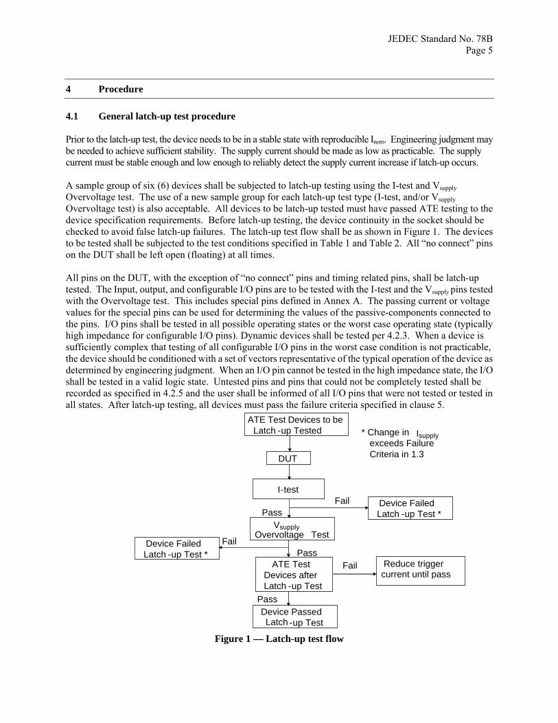
4 Procedure 4.1 General latch-up test procedure Prior to the latch-up test, the device needs to be in a stable state with reproducible Inom. Engineering judgment may be needed to achieve sufficient stability. The supply current should be made as low as practicable. The supply current must be stable enough and low enough to reliably detect the supply current increase if latch-up occurs. A sample group of six (6) devices shall be subjected to latch-up testing using the I-test and Vsupply Overvoltage test. The use of a new sample group for each latch-up test type (I-test, and/or Vsupply Overvoltage test) is also acceptable. All devices to be latch-up tested must have passed ATE testing to the device specification requirements. Before latch-up testing, the device continuity in the socket should be checked to avoid false latch-up failures. The latch-up test flow shall be as shown in Figure 1. The devices to be tested shall be subjected to the test conditions specified in Table 1 and Table 2. All “no connect” pins on the DUT shall be left open (floating) at all times. All pins on the DUT, with the exception of “no connect” pins and timing related pins, shall be latch-up tested. The Input, output, and configurable I/O pins are to be tested with the I-test and the Vsupply pins tested with the Overvoltage test. This includes special pins defined in Annex A. The passing current or voltage values for the special pins can be used for determining the values of the passive-components connected to the pins. I/O pins shall be tested in all possible operating states or the worst case operating state (typically high impedance for configurable I/O pins). Dynamic devices shall be tested per 4.2.3. When a device is sufficiently complex that testing of all configurable I/O pins in the worst case condition is not practicable, the device should be conditioned with a set of vectors representative of the typical operation of the device as determined by engineering judgment. When an I/O pin cannot be tested in the high impedance state, the I/O shall be tested in a valid logic state. Untested pins and pins that could not be completely tested shall be recorded as specified in 4.2.5 and the user shall be informed of all I/O pins that were not tested or tested in all states. After latch-up testing, all devices must pass the failure criteria specified in clause 5.
Figure 1 — Latch-up test flow
ATE Test Devices to be
Latch
Reduce trigger current until pass
Latch -up Tested
DUT
I-test
VsupplyOvervoltage Test
ATE Test Devices after Latch -up Test
Device Passed -up Test
Device Failed Latch - up Test *
Device Failed Latch - up Test *
Fail
Fail
Pass
Pass
* Change in Isupply exceeds Failure Criteria in 1.3
Fail
Pass

JEDEC Standard No. 78B Page 6
4 Procedure (cont’d) 4.1 General latch-up test procedure (cont’d)
Table 1 — Test matrix [7]
Test type Trigger polarity
Condtion of untested
input pins
Test temperature classification
(+/- 2 °C)
Vsupply conditions
Trigger test conditions
Failure criteria [5, 6]
Max Logic High [1] POSITIVE
see Figure 5 Min Logic Low [1]
Per Classification
levels in Section 1.3 [3]
Max Logic High [1]
I-Test
NEGATIVE see Figure 6 Min Logic
Low [1]
Per Classification
levels in Section 1.3 [4]
Max Logic High [1] Vsupply
Over-voltage test
See Figure 7 Min Logic Low [1]
Temperature Class I
Room
Temperature
Maximum operating
voltage for each Vsupply pin
group per device
specification 1.5 X max. Vsupply [2]
Max Logic High [1] POSITIVE
see Figure 5 Min Logic Low [1]
Per Classification
levels in Section 1.3 [3]
Max Logic High [1]
I-Test
NEGATIVE see Figure 6 Min Logic
Low [1]
Per Classification
levels in Section 1.3 [4]
Max Logic High [1] Vsupply
Over-voltage test
See Figure 7 Min Logic Low [1]
Temperature Class II
Maximum ambient
operating temperature
Maximum operating
voltage for each Vsupply pin
group per device
specification 1.5 X max. Vsupply [2]
If absolute Inom is
< 25 mA, then
absolute Inom + 10
mA is used
Or
If absolute Inom is
> 25 mA, then > 1.4 X absolute Inom is used
1. Max. logic high and min. logic low shall be per the device specification. When logic levels are used
with respect to non-digital device it means the maximum high or minimum low voltage the can be supplied to the pin per the device specification.
2. Current clamped at (Inom + 100 mA) or 1.5X Inom, whichever is greater. (Refer to 2.11 for max. Vsupply definition.) The Inom value used for the current clamp calculation relates to the Vsupply pin (or pin groups) being tested.
3. Voltage clamped at Vmax + 0.5(Vmax – Vmin) if Vmin is > 0. Otherwise, the voltage clamp is 1.5 Vmax. 4. Voltage clamped at Vmin – 0.5(Vmax – Vmin) if Vmin is > 0. Otherwise, the voltage clamp is -0.5 Vmax. 5. If the trigger test condition reaches the voltage of current clamp limit and latch-up has not occurred, the
pin passes the latch-up test. See clause 5 for the complete failure definition. 6. The Inom value used for the failure criteria relates to each Vsupply pin (or pin groups) being tested. All
Vsupplies should be monitored, not just the Inom supply for the pin under test. 7. The trigger conditions herein are not indicative of appropriate trigger conditions for all devices.
Appropriate trigger conditions may be more or less stringent. When trigger conditions used in testing differ from this table, the trigger conditions used must be defined in the test results.
JEDEC Standard No. 78B Page 7
4 Procedure (cont’d) 4.1 General latch-up test procedure (cont’d)
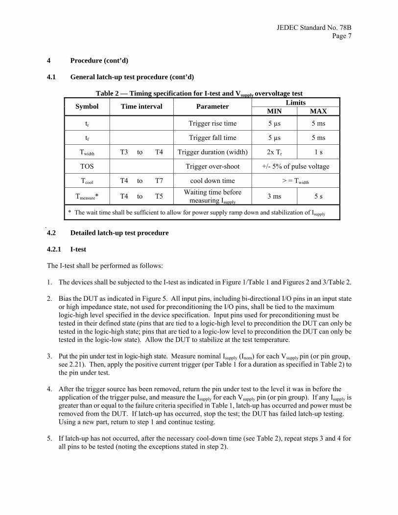
Table 2 — Timing specification for I-test and Vsupply overvoltage test Limits Symbol Time interval Parameter
MIN MAX
tr Trigger rise time 5 µs 5 ms
tf Trigger fall time 5 µs 5 ms
Twidth T3 to T4 Trigger duration (width) 2x Tr 1 s
TOS Trigger over-shoot +/- 5% of pulse voltage
Tcool T4 to T7 cool down time > = Twidth
Tmeasure* T4 to T5 Waiting time before measuring Isupply
3 ms 5 s
* The wait time shall be sufficient to allow for power supply ramp down and stabilization of Isupply
4.2 Detailed latch-up test procedure 4.2.1 I-test The I-test shall be performed as follows: 1. The devices shall be subjected to the I-test as indicated in Figure 1/Table 1 and Figures 2 and 3/Table 2. 2. Bias the DUT as indicated in Figure 5. All input pins, including bi-directional I/O pins in an input state
or high impedance state, not used for preconditioning the I/O pins, shall be tied to the maximum logic-high level specified in the device specification. Input pins used for preconditioning must be tested in their defined state (pins that are tied to a logic-high level to precondition the DUT can only be tested in the logic-high state; pins that are tied to a logic-low level to precondition the DUT can only be tested in the logic-low state). Allow the DUT to stabilize at the test temperature.
3. Put the pin under test in logic-high state. Measure nominal Isupply (Inom) for each Vsupply pin (or pin group,
see 2.21). Then, apply the positive current trigger (per Table 1 for a duration as specified in Table 2) to the pin under test.
4. After the trigger source has been removed, return the pin under test to the level it was in before the
application of the trigger pulse, and measure the Isupply for each Vsupply pin (or pin group). If any Isupply is greater than or equal to the failure criteria specified in Table 1, latch-up has occurred and power must be removed from the DUT. If latch-up has occurred, stop the test; the DUT has failed latch-up testing. Using a new part, return to step 1 and continue testing.
5. If latch-up has not occurred, after the necessary cool-down time (see Table 2), repeat steps 3 and 4 for
all pins to be tested (noting the exceptions stated in step 2).
JEDEC Standard No. 78B Page 8
4.2 Detailed latch-up test procedure (cont’d) 4.2.1 I-test (cont’d) 6. Repeat steps 2 through 5 with all input pins, including bi-directional I/O pins in an input state or high
impedance state, not used for preconditioning the I/O pins tied to the minimum logic-low level specified in the device specification.
7. Bias the DUT as indicated in Figure 6 with all input pins, including bi-directional I/O pins in an input
state or high impedance state, not used for preconditioning the I/O pins shall be tied to the maximum logic-high level specified in the device specification (noting the exceptions stated in step 2).
8. Put the pin under test in logic-low state. Measure nominal Isupply (Inom) for each Vsupply pin (or pin group,
see 2.21). Then, apply the negative current trigger source below ground (per Table 1 for a duration as specified in Table 2) to the pin under test.
9. After the trigger source has been removed, return the pin under test to the level it was in before the
application of the trigger pulse and measure the Isupply for each Vsupply pin (or pingroup). If any Isupply is greater than or equal to the failure criteria specified in Table 1, latch-up has occurred and power must be removed from the DUT. If latch-up has occurred, stop the test; the DUT has failed latch-up testing. Using a new part, return to step 1 and continue testing.
10. If latch-up has not occurred, after the necessary cool-down time (see Table 2), repeat steps 8 and 9 for
all pins to be tested. 11. Repeat steps 8 through 10 with all input pins, including bi-directional I/O pins in an input state or high
impedance state, not used for preconditioning the I./O pins tied to the minimum logic-low level specified in the device specification (noting the exceptions stated in step 2).
I-test in 4.2.1 does not require the removal of power-supply voltage between stresses, i.e., cool-down time. Users should evaluate the risk of leaving the power-supply on.
JEDEC Standard No. 78B Page 9
4.2 Detailed latch-up test procedure (cont’d)
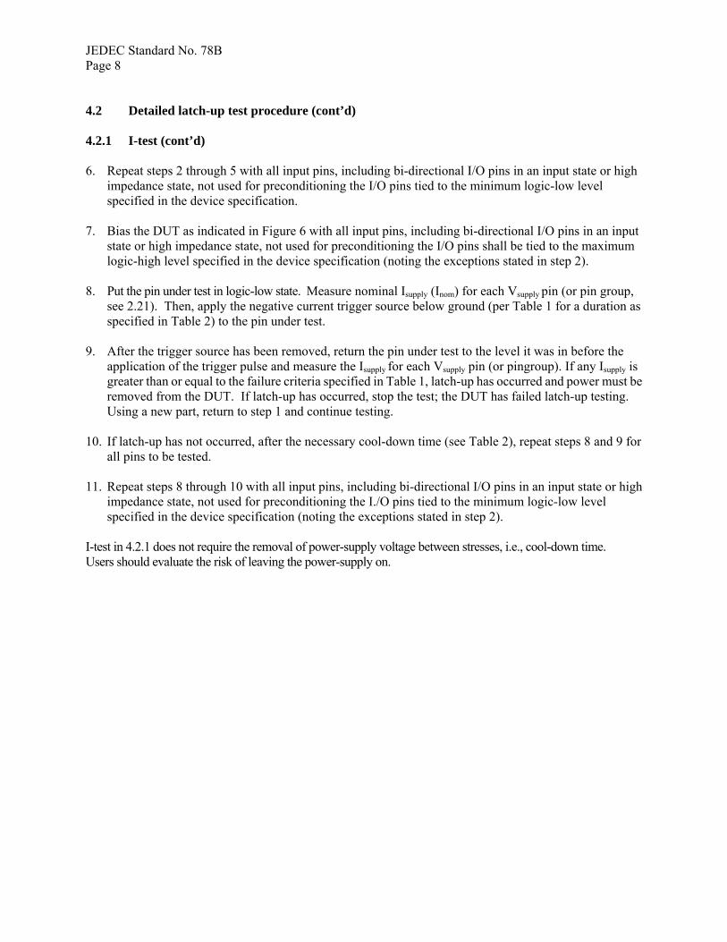
Figure 2 — Test waveform for positive I-test
** Max. logic high and min. logic low shall be per the device specification. When logic levels are used with respect to a non-digital device, it means the maximum high or minimum low voltage that can be supplied to the pin per the device specification.
* The wait time shall be sufficient to allow for power supply ramp down and stabilization of Isupply
90%
T1 T2 T3 T4 T5 T6
Max. V supply
V supply PIN
PIN UNDER TEST
t r t f t r
TOS TOS
Max. Logic High **
T7
GND
GND
Time Operation
T1 → T2 Measure nominal Isupply (Inom) T4 → T7 Cool down time (Tcool) T4 → T5 Wait time prior to Isupply measurement. * T5 Measure Isupply
T6 If any Isupply ≥ the failure criteria defined in 1.3, latch-up has occurred and power must be removed from DUT.
TOS
+(I nom + 100 mA) or +1.5X I nom, whichever is greater
I trigger
*** The pin under test shall be set to logic high before positive current trigger. It is permissible to start positive current trigger from logic low, but failing results should be confirmed from the logic high state.
Figure 3 — Test waveform for negative I-test
** Max. logic high and min. logic low shall be per the device specification. When logic levels are used with respect to a non-digital device, it means the maximum high or minimum low voltage that can be supplied to the pin per the device specification.
* The wait time shall be sufficient to allow for power supply ramp down and stabilization of Isupply.
90%
T1 T2 T3 T4 T5 T6I trigger
TOS
Min. Logic Low ** t r t f
PIN UNDER TEST
Max. V supply
V supply PIN GND
t r TOS
- 100 mA or -.5X Inom, whichever is greater
T7
T1 → T2 Measure nominal Isupply (Inom) T4 → T7 Cool down time (Tcool) T4 → T5 Wait time prior to Isupply measurement. * T5 Measure Isupply
T6 If any Isupply ≥ the failure criteria defined in 1.3, latch-up has occurred and power must be removed from DUT.
Time Operation
*** The pin under test shall be set to logic low before negative current trigger. It is permissible to start negative current trigger from logic high, but failing results should be confirmed from the logic low state.
JEDEC Standard No. 78B Page 10
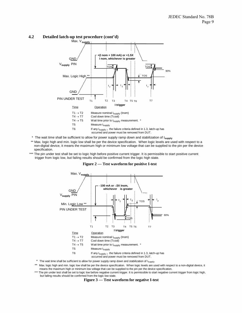
4.2 Detailed latch-up test procedure (cont’d) 4.2.2 Vsupply overvoltage test The Vsupply overvoltage test shall be performed on each Vsupply pin (or pin group) as indicated below. To provide a true indication of latch-up for given test conditions input pins configured as logic-high shall remain within the valid logic-high region as defined in the device specification (typically greater than 70% of the Vsupply overvoltage test level). If input pin levels fall outside of the valid logic-high region, the device may change state causing a change in Inom and invalid test data. If a latch-up failure occurs when the input pin(s) fall outside of the valid logic-high region, engineering judgment must be used to determine whether the failure is a valid latch-up condition or a failure caused by a change in state. 1. The devices shall be subjected to the Vsupply overvoltage test as indicated in Figure l/Table 1 and Figure
4/Table 2. 2. Bias the DUT as indicated in Figure 7. All input pins, including bi-directional I/O pins in an input state
or high impedance state, not used for preconditioning the I/O pins shall be tied to the maximum logic-high level specified in device specification. Input pins used for preconditioning must be tested in their defined state (pins that are tied to a logic-high level to precondition the DUT can only be tested in the logic-high state, pins that are tied to a logic-low level to precondition the DUT can only be tested in the logic-low state). Allow the DUT to stabilize at the test temperature. Measure nominal Isupply (Inom) for each Vsupply pin (or pin group, see 2.21) at this time.
3. Apply the voltage trigger source (per Table 1 for a duration as specified in Table 2) to the Vsupply pin (or
pin group) under test. 4. After the trigger source has been removed, return the Vsupply pin under test to the state it was in before
the application of the trigger pulse and measure the Isupply for each Vsupply pin (or pin group). If any Isupply is greater than or equal to the failure criteria specified in 1.3, latch-up has occurred and power must be removed from the DUT. If latch-up has occurred stop the test; the DUT has failed latch-up testing. Using a new part, return to step 1 and continue testing.
5. If latch-up has not occurred, after the necessary cool-down time (see Table 2), repeat steps 2
through 4 with all input pins, including bi-directional I/O pins in an input state or high impedance state, not used for preconditioning the I/O pins tied to the minimum logic-low level specified in the device specification (noting the exceptions stated in step 2).
6. Repeat steps 2 through 5 until each Vsupply pin (or pin group) has been tested.
JEDEC Standard No. 78B Page 11
4.2 Detailed latch-up test procedure (cont’d) 4.2.2 Vsupply overvoltage test (cont’d)
90%
10%
T1 T2 T3 T4 T5 T6
t r t f t r
TOS TOS
V supply PIN T7
Max.V supply
GND
1.5 X max. V supply (max. refers to the magnitude of V supply and can be either positive or negative)
T1 → T2 Measure nominal Isupply (Inom) T4 → T7 Cool down time (Tcool) T4 → T5 W ait time prior to Isupply measurement. * T5 Measure Isupply
T6 If any Isupply ≥ the failure criteria defined in 1.3, latch-up has occurred and power must be removed from then on.
Time Operation
NOTE The wait time shall be sufficient to allow for power supply ramp down and stabilization of Isupply.
Figure 4 — Test waveform for Vsupply overvoltage 4.2.3 Testing dynamic devices Devices that during normal operating conditions have a clock and/or other timing signal inputs may be latch-up tested in a static manner as indicated in 4.2.1 and 4.2.2. If the device does not show a stable Isupply (Inom) measurement or appears to latch up, the clock and/or other associated timing and control signals, as defined in the device specification, may be applied to the device during latch-up testing per 4.2.1 and 4.2.2. Unless otherwise specified, the clock pins and other associated timing pins used to place the device in a stable state shall not be latch-up tested while being used to stabilize the device. The supplier shall maintain records indicating how the device was tested, as indicated in 4.2.5. 4.2.4 DUT disposition Latch-up testing is potentially destructive. Devices used for latch-up testing shall not be used or considered as salable devices. 4.2.5 Record keeping Data shall be recorded for each pin failure and shall include the test condition (clock frequency for dynamic devices, if used), vector set used for preconditioning, temperature, trigger condition, and latch-up Isupply current. Data shall also be recorded for all pins and operating states that could not be completely tested per 4.2.3. This information shall identify the pins, operating states, and reason for incomplete testing. The supplier shall report the integrated circuit classification Class I or Class II per 1.1. The stress level the integrated circuit passed shall be reported: level A or Level B per 1.2. The Level B current injection value applied shall be reported per pin.
JEDEC Standard No. 78B Page 12
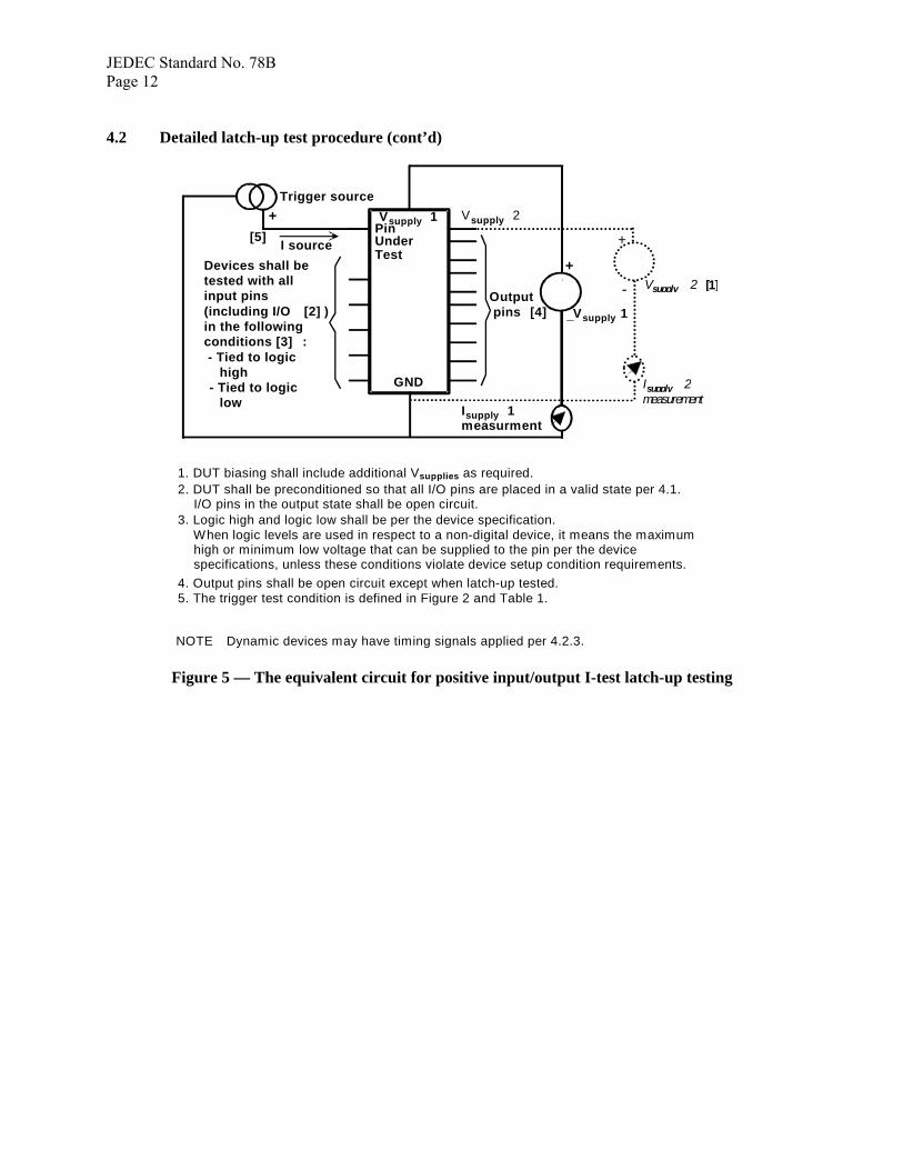
4.2 Detailed latch-up test procedure (cont’d)
Vsupply 2+Trigger source
+
_Vsupply 1
GND
PinUnderTest
I source
Isupply 2measurement
+
- Vsupply 2 [1]
Isupply 1measurment
Vsupply 1
Output pins [4]
Devices shall betested with allinput pins(including I/O [2] )in the followingconditions [3] : - Tied to logic high- Tied to logic
low
[5]
1. DUT biasing shall include additional Vsupplies as required. 2. DUT shall be preconditioned so that all I/O pins are placed in a valid state per 4.1.
I/O pins in the output state shall be open circuit. 3. Logic high and logic low shall be per the device specification. When logic levels are used in respect to a non-digital device, it means the maximum
high or minimum low voltage that can be supplied to the pin per the device specifications, unless these conditions violate device setup condition requirements.
4. Output pins shall be open circuit except when latch-up tested. 5. The trigger test condition is defined in Figure 2 and Table 1.
NOTE Dynamic devices may have timing signals applied per 4.2.3.
Figure 5 — The equivalent circuit for positive input/output I-test latch-up testing
JEDEC Standard No. 78B Page 13
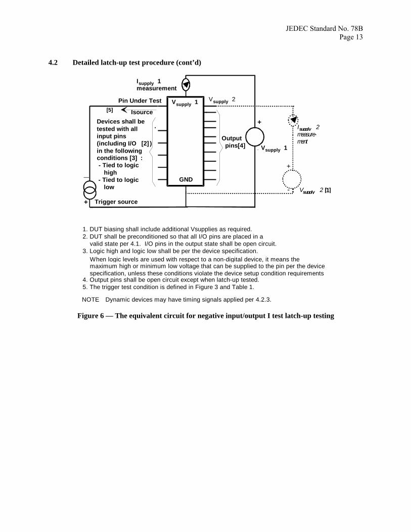
4.2 Detailed latch-up test procedure (cont’d)
Vsupply 2
+
_
Trigger source
Vsupply 1
+
_
GND
Vsupply 1
Pin Under Test
Isource
Isupply 2measure-ment
+
- Vsupply 2 [1]
Isupply 1measurement
Output pins[4]
Devices shall betested with allinput pins(including I/O [2] )in the followingconditions [3] : - Tied to logic high- Tied to logic low
[5]
1. DUT biasing shall include additional Vsupplies as required. 2. DUT shall be preconditioned so that all I/O pins are placed in a valid state per 4.1. I/O pins in the output state shall be open circuit. 3. Logic high and logic low shall be per the device specification. When logic levels are used with respect to a non-digital device, it means the maximum high or minimum low voltage that can be supplied to the pin per the device specification, unless these conditions violate the device setup condition requirements 4. Output pins shall be open circuit except when latch-up tested. 5. The trigger test condition is defined in Figure 3 and Table 1.
NOTE Dynamic devices may have timing signals applied per 4.2.3.
Figure 6 — The equivalent circuit for negative input/output I test latch-up testing
JEDEC Standard No. 78B Page 14
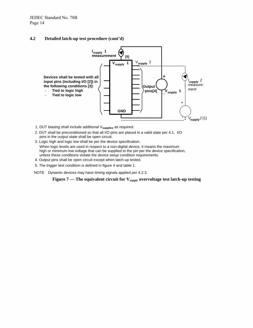
4.2 Detailed latch-up test procedure (cont’d)
V supply 2
I supply 2 measure- ment
+
- V supply 2 [1]
V supply 1
+
_
GND
V supply 1
I supply 1 measurement
Devices shall be tested with all input pins (including I/O [2]) in the following conditions [3]: – Tied to logic high – Tied to logic low
Output pins[4]
[5]
1. DUT biasing shall include additional Vsupplies as required. 2. DUT shall be preconditioned so that all I/O pins are placed in a valid state per 4.1. I/O
pins in the output state shall be open circuit. 3. Logic high and logic low shall be per the device specification.
When logic levels are used in respect to a non-digital device, it means the maximum high or minimum low voltage that can be supplied to the pin per the device specification, unless these conditions violate the device setup condition requirements.
4. Output pins shall be open circuit except when latch-up tested. 5. The trigger test condition is defined in figure 4 and table 1.
NOTE Dynamic devices may have timing signals applied per 4.2.3. Figure 7 — The equivalent circuit for Vsupply overvoltage test latch-up testing
JEDEC Standard No. 78B Page 15
5 Failure criteria A device that fails one or more of the following conditions is considered a failure: 1. Device does not pass the test requirements in Table 1. 2. Device no longer meets functional, parametric or I/V requirements of the device specification. A device is considered a failure if the device does not pass the test requirements in Table 1. In addition, ATE testing is required following latch-up test for the following two reasons. – Latch-up events triggered during over-voltage or current injection tests may damage the device, and the
damage could end the latch-up event before the latch-up tester detects the failure (short-duration latch-up). An ATE test failure may be the only indication of this latch-up.
– Latch-up test current injection could directly damage the DUT through EOS without an actual latch-up
event. This damage source, or damage from undetected, short-duration latch-up events, may prevent proper control of the device during latch-up testing and invalidate the latch-up test results. ATE testing can be used to confirm this device damage.
If an integrated circuit fails the ATE test after the latch-up stress, adjust the input trigger current to a value at which the integrated circuit can pass. The integrated circuit falls in Class B. See 4.2.5 for reporting the pass value. 6 Summary The following details shall be specified in the procurement document, if different from the requirements in this specification: 1 Class (I or II) per this document.
2 Sample size.
3 Trigger test conditions.
4 Latch-up test temperature.
5 Failure criteria (if not Level A per 1.2).
6 Pulse/Trigger conditions.
7 Vector set used to precondition the device.
JEDEC Standard No. 78B Page 16
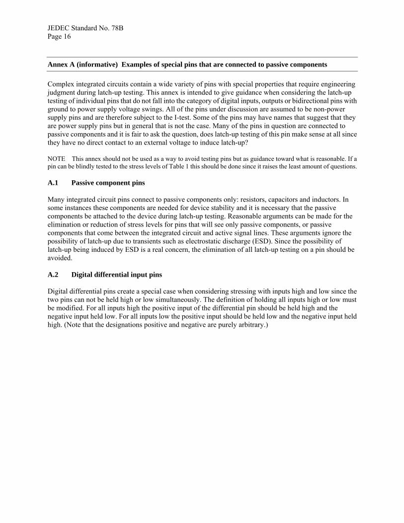
Annex A (informative) Examples of special pins that are connected to passive components Complex integrated circuits contain a wide variety of pins with special properties that require engineering judgment during latch-up testing. This annex is intended to give guidance when considering the latch-up testing of individual pins that do not fall into the category of digital inputs, outputs or bidirectional pins with ground to power supply voltage swings. All of the pins under discussion are assumed to be non-power supply pins and are therefore subject to the I-test. Some of the pins may have names that suggest that they are power supply pins but in general that is not the case. Many of the pins in question are connected to passive components and it is fair to ask the question, does latch-up testing of this pin make sense at all since they have no direct contact to an external voltage to induce latch-up? NOTE This annex should not be used as a way to avoid testing pins but as guidance toward what is reasonable. If a pin can be blindly tested to the stress levels of Table 1 this should be done since it raises the least amount of questions. A.1 Passive component pins Many integrated circuit pins connect to passive components only: resistors, capacitors and inductors. In some instances these components are needed for device stability and it is necessary that the passive components be attached to the device during latch-up testing. Reasonable arguments can be made for the elimination or reduction of stress levels for pins that will see only passive components, or passive components that come between the integrated circuit and active signal lines. These arguments ignore the possibility of latch-up due to transients such as electrostatic discharge (ESD). Since the possibility of latch-up being induced by ESD is a real concern, the elimination of all latch-up testing on a pin should be avoided. A.2 Digital differential input pins Digital differential pins create a special case when considering stressing with inputs high and low since the two pins can not be held high or low simultaneously. The definition of holding all inputs high or low must be modified. For all inputs high the positive input of the differential pin should be held high and the negative input held low. For all inputs low the positive input should be held low and the negative input held high. (Note that the designations positive and negative are purely arbitrary.)
JEDEC Standard No. 78B Page 17
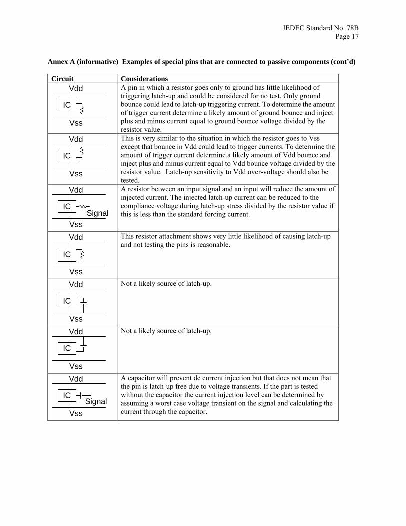
Annex A (informative) Examples of special pins that are connected to passive components (cont’d) Circuit Considerations
IC
Vss
Vdd
A pin in which a resistor goes only to ground has little likelihood of triggering latch-up and could be considered for no test. Only ground bounce could lead to latch-up triggering current. To determine the amount of trigger current determine a likely amount of ground bounce and inject plus and minus current equal to ground bounce voltage divided by the resistor value.
IC
Vss
Vdd
This is very similar to the situation in which the resistor goes to Vss except that bounce in Vdd could lead to trigger currents. To determine the amount of trigger current determine a likely amount of Vdd bounce and inject plus and minus current equal to Vdd bounce voltage divided by the resistor value. Latch-up sensitivity to Vdd over-voltage should also be tested.
IC
Vss
Vdd
Signal
A resistor between an input signal and an input will reduce the amount of injected current. The injected latch-up current can be reduced to the compliance voltage during latch-up stress divided by the resistor value if this is less than the standard forcing current.
IC
Vss
Vdd
This resistor attachment shows very little likelihood of causing latch-up and not testing the pins is reasonable.
IC
Vss
Vdd
Not a likely source of latch-up.
IC
Vss
Vdd
Not a likely source of latch-up.
IC
Vss
Vdd
Signal
A capacitor will prevent dc current injection but that does not mean that the pin is latch-up free due to voltage transients. If the part is tested without the capacitor the current injection level can be determined by assuming a worst case voltage transient on the signal and calculating the current through the capacitor.
JEDEC Standard No. 78B Page 18
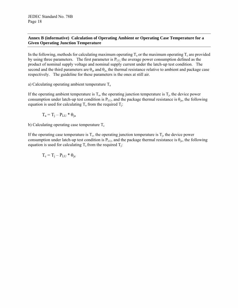
Annex B (informative) Calculation of Operating Ambient or Operating Case Temperature for a Given Operating Junction Temperature In the following, methods for calculating maximum operating Ta or the maximum operating Tc are provided by using three parameters. The first parameter is PLU, the average power consumption defined as the product of nominal supply voltage and nominal supply current under the latch-up test condition. The second and the third parameters are θja and θjc, the thermal resistance relative to ambient and package case respectively. The guideline for these parameters is the ones at still air. a) Calculating operating ambient temperature Ta If the operating ambient temperature is Ta, the operating junction temperature is Tj, the device power consumption under latch-up test condition is PLU, and the package thermal resistance is θja, the following equation is used for calculating Ta from the required Tj: Ta = Tj – PLU * θja b) Calculating operating case temperature Tc If the operating case temperature is Tc, the operating junction temperature is Tj, the device power consumption under latch-up test condition is PLU, and the package thermal resistance is θjc, the following equation is used for calculating Tc from the required Tj: Tc = Tj – PLU * θjc
JEDEC Standard No. 78B Page 19
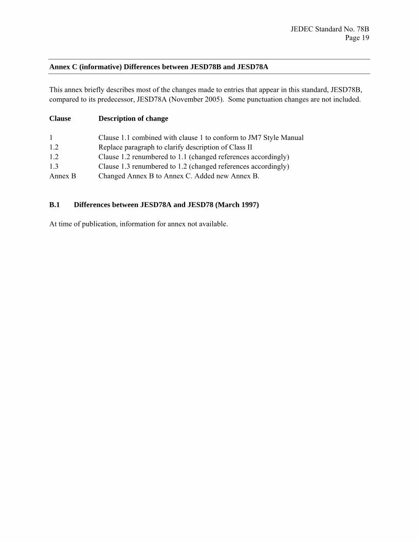
Annex C (informative) Differences between JESD78B and JESD78A
This annex briefly describes most of the changes made to entries that appear in this standard, JESD78B, compared to its predecessor, JESD78A (November 2005). Some punctuation changes are not included. Clause Description of change 1 Clause 1.1 combined with clause 1 to conform to JM7 Style Manual 1.2 Replace paragraph to clarify description of Class II 1.2 Clause 1.2 renumbered to 1.1 (changed references accordingly) 1.3 Clause 1.3 renumbered to 1.2 (changed references accordingly) Annex B Changed Annex B to Annex C. Added new Annex B. B.1 Differences between JESD78A and JESD78 (March 1997) At time of publication, information for annex not available.

JEDEC Standard No. 78B Page 20

Standard Improvement Form JEDEC JESD78B The purpose of this form is to provide the Technical Committees of JEDEC with input from the industry regarding usage of the subject standard. Individuals or companies are invited to submit comments to JEDEC. All comments will be collected and dispersed to the appropriate committee(s). If you can provide input, please complete this form and return to: JEDEC Attn: Publications Department 3103 North 10th Street, Suite 240 South Arlington, VA 22201
Fax: 703.907.7583
1. I recommend changes to the following: Requirement, clause number
Test method number Clause number
The referenced clause number has proven to be: Unclear Too Rigid In Error Other
2. Recommendations for correction:
3. Other suggestions for document improvement:
Submitted by Name: Phone:
Company: E-mail:
Address:
City/State/Zip: Date: