İstanbul technİcal university electrİcal –...
TRANSCRIPT

i
İSTANBUL TECHNİCAL UNIVERSITY
ELECTRİCAL – ELECTRONICS ENGINEERING FACULTY
WRITING DRIVERS FOR CUSTOM PERIPHERAL RUNNİNG PARALLEL
TO MICROBLAZE PROCESSOR ON FPGA
BSc Thesis by
Engin YÜREK
Department: Electronics and Communication Engineering
Programme: Electronics and Communication Engineering
Supervisor: Assoc. Prof. Dr. Sıddıka Berna ÖRS YALÇIN
MAY 2016

i
Abstract
Although computation power of microprocessors increases within the development
of technology, in recent years, with the increase of the connectivity of all kind of
devices and escalating raw data amount requires computation power more than ever.
To meet the demands of software side, some regulations is needed in hardware side
in favor of microprocessors work by not deluding but performing real multitasking
with the way of employing special purpose peripherals which undertake some set of
instructions from processor unit and work parallel with it. In the light of all the facts
mentioned above a barebone softcore microprocessor and a custom peripheral can be
embedded on a field programmable gate array via using the features of Xilinx
development tools. In this context an example of above idea is realized and explained
step by step through the thesis. Firstly, a MicroBlaze project is created with some
built-in peripherals, then a custom a custom peripheral is added and rearranged to
have extra interrupt ports. After this step an eight-bit serial adder module is
implemented into this peripheral. Thus all eight-bit addition operations can be done
on this peripheral instead of running on microprocessor. Finally, driver functions and
a general purpose interrupt service routine is written with C language via Software
Development Kit provided by Xilinx.

ii
CONTENTS
ABSTRACT III
ABBREVIATIONS IV
LIST OF FIGURES V
SUMMARY VI
1. INTRODUCTION
2. TOOLS USED IN PROJECT
2.1 Field Programmable Gate Array (FPGA)
2.2 MicroBlaze Soft Core Processor
2.3 Xilinx Platform Studio (XPS)
2.4 Integrated Synthesis Environment (ISE)
2.5 Software Development Kit (SDK)
3. CREATING MICROBLAZE PROCESSOR ON XPS
3.1 Creating MicroBlaze Core Project
3.2 Attaching AXI Timer
3.3 Attaching AXI Interrupt Controller
4. ADDING CUSTOM IP (INTELLECTUAL PROPERTY)
4.1 Creating Barebone Custom IP
4.2 Adding Interrupt Port to Custom IP
4.3 Adding Custom Feature to IP
4.3.1 Design the Serial Adder
4.3.2 Implementation of Serial Adder into IP
4.3 Connecting Custom IP to Interrupt Controller

iii
5. INTERRUPT HANDLING ON SOFTWARE SIDE (STANDALONE)
5.1 Creating Project and Writing Interrupt Handler Code
5.2 Running Project on Digilent Atlys Spartan-6 Board
6.CONCLUSION

iv
ABBREVIATIONS
XMD : Xilinx microprocessor Debugger
AMBA : Advanced Microprocessor Bus Architecture
UART : Universal Asynchronous Receiver Transmitter
ALU : Arithmetic Logic Unit
QuadSPI : Quad Serial Peripheral Interface
GIPO : General Purpose Input Output
IRQ : Interrupt Request
MSR : Machine Status Register
PLB : Processor Local Bus
AXI : Advanced Extensible Interface
RISC : Reduced Instruction Set
LUT : Look-up Table
HDL : Hardware Definition Language
RAM : Random Access Memory
USB : Universal Serial Bus
XPS : Xilinx Platform Studio
IPIF : Intellectual Property Interface
MPD : Microprocessor Peripheral Definition
SVN : Source Version Control
SDK : Software Development Kit
DVI : Digital Visual Interface
HDMI : High Definition Multimedia Interface
EDK : Embedded Development Kit
LUT : Look-up Table
EEPROM : Electrically Erasable Programmable Read Only Memory
FPGA : Field Programmable Gate Array
BRAM : Block Random Access Memory
ISE : Integrated Synthesis Environment
I2C : Inter-Integrated Circuit
RTL : Register Transfer Level
QSPI : Queued Serial Peripheral Interface
FSL : Fast Simplex Link
IP : Intellectual Property
BFM : Bus Functional Model
CPU : Central Processing Unit
MPD : Microprocessor Peripheral Definition
JTAG : Joint Test Action Group
USB : Universal Serial Bus
BSB : Board Support Package

v
LIST OF FIGURES
Figure 1: Internal Structure of Logical Block .............................................................. 3
Figure 2: Block Structure of MicroBlaze [6] ............................................................... 4
Figure 3: Read- Write Operations of AXI4 and AXI4-Lite [9] ................................... 5
Figure 4: Main Interface of ISE ................................................................................... 7
Figure 5: Project Creation Menu of XPS ..................................................................... 8
Figure 6:XPS Create Project Window ......................................................................... 9
Figure 7: Base System Builder Board Configuration ................................................ 10
Figure 8: Microprocessor Configuration .................................................................... 11
Figure 9: Main Interface of XPS ................................................................................ 12
Figure 10: AXI Timer ................................................................................................ 12
Figure 11: Core configuration of axi_timer ............................................................... 13
Figure 12: Automatic Wiring Window ...................................................................... 13
Figure 13: AXI Interrupt Controller ........................................................................... 14
Figure 14: Assigning Timer Interrupt ........................................................................ 14
Figure 15:Interrupt Connection Dialog ...................................................................... 14
Figure 16: Connecting Interrupt Controller to MicroBlaze ....................................... 15
Figure 17: XPS Graphical View ................................................................................ 15
Figure 18: Custom IP Creation Menu ........................................................................ 16
Figure 19: Create and Import Peripheral Wizard ....................................................... 17
Figure 20:Create Peripheral Window......................................................................... 17
Figure 21: Peripheral Name and Version Configuration ........................................... 18
Figure 22: Bus interface Selection ............................................................................. 19
Figure 23: IP interface configuration ......................................................................... 20
Figure 24: Software Accessible Register Selection ................................................... 21
Figure 25: IP Interconnect Signals ............................................................................. 21
Figure 26: Peripheral Implementation Support .......................................................... 22
Figure 27: Newly Created IP...................................................................................... 22
Figure 28: Adding Extra Port to Custom IP .............................................................. 23
Figure 29: Defining Extra Port ................................................................................... 24
Figure 30:Adding Extra Port to eight_bit_adder Top Module ................................... 24
Figure 31: Definition of Port in Top Module ............................................................. 24
Figure 32: Connection Between the Modules ............................................................ 24
Figure 33: RTL SerialAdder module ......................................................................... 25
Figure 34: Pao file of IP ............................................................................................. 26
Figure 35: Addition of SerialAdder.v ........................................................................ 26
Figure 36: Net Declarations ....................................................................................... 26
Figure 37: Submodule Decleration ............................................................................ 27
Figure 38:Assignment of Output ................................................................................ 27
Figure 39:Commenting Third Register ...................................................................... 28
Figure 40: Assign Done Signal to Interrupt Port ....................................................... 28
Figure 41: Interrupt Port Definition in MPD File ...................................................... 28
Figure 42: Rescan User Repositories ......................................................................... 29
Figure 43: Adding Custom IP to Project .................................................................... 29
Figure 44: Assign Number of Register ...................................................................... 30

vi
Figure 45: Attaching Adder to Interrupt List ............................................................. 30
Figure 46: Export Design Into SDK........................................................................... 31
Figure 47 :Choosing Works Space ............................................................................. 31
Figure 48: Adding Repositories (a) ............................................................................ 32
Figure 49: Adding Repositories (b) ........................................................................... 32
Figure 50: Application Project Creation .................................................................... 32
Figure 51: Create Projet Wizard ................................................................................ 33
Figure 52: Correct Error in Test File ......................................................................... 34
Figure 53: JTAG Configuration (a)............................................................................ 34
Figure 54: Jtag Configuration (b) ............................................................................... 35
Figure 55: Run configuration (a) ............................................................................... 35
Figure 56: STDIO in Console .................................................................................... 36
Figure 57: Generate Linker Script (a) ........................................................................ 36
Figure 58: Generate Linker Script (b) ........................................................................ 37
Figure 59: Run Project on Board ............................................................................... 37

1
INTRODUCTION
Within the dramatic increase in amount of data causes longer process time
which is a huge problem for time dependent projects especially real time
applications. To overcome this problem burden of main processor should be
distributed in peripherals. Thus discrete operations would not wait each other and
will be able to processed at the same time in different peripherals which is far better
approach than multithreading. A simple example of this scenario is demonstrated
through the thesis in a generic way to make this document like a step by step guide
for future use. Firstly, hardware and software tools that are used during the thesis is
described shortly in different subheadings. Then a general purpose MicroBlaze
processor is created with external AXI timer and interrupt controller peripherals.
Afterwards, a custom peripheral is created via Create and Import Peripheral Wizard
and an extra port is added for interrupt signal. Next, an unsigned eight-bit serial
adder module is created and embedded into custom peripheral then design is
exported to higher level software kit and by this way hardware side of the project is
finished. In software side interrupt structure is established via interrupt controller
framework and an interrupt service routine is written to handle interrupt signals
coming from the adder module. Finally, demonstration of the project is shown on
real FPGA board.

2
2. TOOLS USED IN PROJECT
2.1 Field Programmable Gate Arrays (FPGA)
Field programmable gate array (FPGA) [1]is an integrated circuit which has
no intendent function but has the opportunity to convert FPGA into anything such as
digital signal processor, custom drivers, processors etc. Though with the help of this
flexibility, FPGAs has ability to be programmed in an attempt to behave as any
desired digital circuit. Instead of wiring up logics manually one can design all of
circuit with the HDL (Hardware Definition Language) [2] code than this chip
handles with it and creates desired circuit physically. This is not simulation of the
circuit with the code but its physical logics so it runs faster than a program runs over
a microcontroller. Since FPGAs are super-fast, they are preferred in random access
memory, high definition multimedia interface and universal serial bus projects. In
addition to those FPGAs also can be programmed as softcore microcontroller and the
good thing is unused logical units can be used for time consuming operations like
dividing or multiplication and all this blocks works perfectly parallel to
microcontroller so that controller unit do not have to spend time for this operations
all it needs to get an interrupt from this external blocks.
FPGA logical units are volatile so whenever the power goes of all the
configuration get lost. To prevent this an FPGA consists built in EEPROM
(Electrically Erasable Programmable Read Only Memory) [3] to store the
configuration of logical blocks. Furthermore, it consists logical blocks, connection
blocks and switch blocks. Logical block is the basic unit of FPGA and a logical
block consists LUTs (Lookup-Table), flip-flops, multiplexers and buffers to
accomplish its duty as seen in Figure-1. LUTs are responsible for implementing
function generators into logical block which are able to realize outcomes of any 4
input Boolean statements. Multiplexer exists for selecting right signal and buffers are
for increasing the signals strength.

3
Figure 1: Internal Structure of Logical Block
Logical blocks came together and creates cluster. The connections between
logical blocks in different clusters are slower than the ones in the same cluster due to
routing losses, matrix like interconnects and switching block delays. Since all logical
blocks has possibility to be get connected for implementing desired circuit most of
the FPGA are is covered with very thin layers of metal roads.
Besides the advantages of the FPGAs, compared to other integrated circuits
they are high priced and since they have lots of metal routes they consume huge
amount of energy. They are volatile and they store the configuration info in the
EEPROM. Therefore, they are not instant on and it takes some time to boot up. In
most cases designing from the lowest level is harder and FPGAs has complicated
data sheets and also HDL is not easy as C, C++ languages.

4
2.2 MicroBlaze Soft Core Processor
MicroBlaze is a softcore microprocessor which means it can be designed with
only using logic synthesis. It is adopted by Xilinx to work compatible with Xilinx
tools and boards [4]. Furthermore, it is adjusted for low cost, minimum power
consumption, relative speed and minimum FPGA source consumption.
The main part of the MicroBlaze system includes 32 general purpose registers
with 32 bit long, an ALU, a shift unit, special purpose registers, program counter,
instruction buffer, and instruction decode cores as show in Figure 2. Besides, the
main design can be expanded and customized by other peripherals such as
barel-shifter, divider, multiplier, instruction and data caches, exception handling and
debug logics etc. to perform more advanced actions.
Figure 2: Block Structure of MicroBlaze [5]
While MicroBlaze is built on one side of FPGA other portions can also be
used for another purposes. Thus there will not be waste of resources and user can use
the exact configuration for the target project and could have the ability of putting
more than one softcore microcontroller with different cores. This also reduces the
cost and size of application.
MicroBlaze is a 32-bit RISC processor with a parallel pipeline which has
three steps fetch, decode and execute to process an instruction. Each stage takes 1
clock cycle to perform its duty. Thus each instruction is performed in three cycles.

5
Since it is a parallel pipeline while an instruction is decoded, another instruction is
fetched form Instruction prefect buffer at the same time.
MicroBlaze supports only one external interrupt source. To work with more
than one external interrupt sources an interrupt controller must be used for handling
multiple interrupt requests. The processor executes interrupt vector only if the
interrupt enable bit in machine status register is set to 1. As interrupt controller is
needed in most projects, Xilinx provides an interrupt controller with the embedded
development kit.
MicroBlaze provides PLB (Processor Local Bus) [6] and AXI (Extensible
interface) [7] bus for the communication and management of functional cores. AXI
uses AMBA (Advanced Microprocessor Bus Architecture) [8] standard for the
communication and has three types (AXI4, AXI4-Lite, AXI4-stream) for different
needs of designs.
AXI4 is preferred for high performance memory mapped requirements.
AXI4-lite is simpler than AXI4 and is preferred for low throughput memory mapped
communication.
AXI4-stream is preferred for high speed data streaming and is not memory mapped.
AXI4 and AXI4-lite uses 5 different channels while data transfer. Thus bidirectional
data transfer can occur at the same time as illustrated in Figure 3.
* Read address channel
* Write address channel
* Read data channel
* Write address channel
* Write address response channel
Figure 3: Read- Write Operations of AXI4 and AXI4-Lite [9]

6
2.3 Xilinx Platform Studio (XPS)
Xilinx platform studio is the graphical user interface that includes set of
intelligent tools and has the ability to abstract system details and lets developers to
design complex structures much more easily and efficiently [10] XPS presents drag-
and-drop aggregation of IP cores from the Xilinx Embedded IP catalog interface,
within custom processor designs. Some of the cores include devices and accelerators
such as AXI bridges, GPIO, PLBV4.6 bridge, BRAM and external memory
controllers, Serial Peripheral and QuadSPI Interfaces, Analog to Digital converters,
Graphics, Clocks and Timers, UARTs, I2C, Interrupt controllers and many others.
With the power of XPS developers boot an embedded system in a few
minutes without facing processor system complexity and performance issues. It also
includes an enhanced IP creation wizard to design hardware peripherals for soft core
processors.
XPS also provides software platform support. After generating hardware
design, it provides option to move Software Development Kit (SDK) and creates an
automatic board support package which includes libraries for interaction with
peripherals.
2.4 Integrated Synthesis Environment (ISE)
ISE is a Xilinx software program which has ability of synthesize and analysis of
HDL (Hardware Description Language) designs [11] By use of this software,
developers can synthesize the design, perform trimming analysis, produce RTL
(Register Transfer Level) schematics, and configure with the program. ISE controls
all this processes through the project navigator.

7
Figure 4: Main Interface of ISE
On the left top side of the panel under the Hierarchy part, design files and
their relation can be seen. Under this part, process panel provides design summary
reports, design utilities, user constraints, synthesis, implement design, generate
programming file and configure target device. At the bottom of project navigator,
console, errors, warnings panel that displays messages can be seen. At the right part,
design and summary report viewer provides detailed reports of design which
gathered during the design processes. At right side of design and summary report
viewer, document interface displays many types of documents and also can be used
as editor of these documents. Reports, design schematics simulation waveforms are
also displayed here. ISE main development window can be seen in Figure 4.
2.5 Software Development Kit (SDK)
Eclipse is an open source software development platform equipped lots of
features and extensible plugin interface to develop and debug software in quite a few
programming languages [12]. Some of its features are the following:
* An interface for writing and compiling C/C++ code with many properties.
*Project organization
*Custom configuration for different build needs and automatic Makefile creation
*Error trace
*Subversion support

8
Therefore, Xilinx adopted this platform into its EDK. Hence one can design a
project hardware on XPS and then migrate to SDK to write its top level code mostly
in C language. In addition to above features Xilinx SDK provides extra features for
Xilinx embedded processors listed below, [12]
*Xilinx Microprocessor Debugger (XMD). Stands for establishing communication
between SDK and FPGA board
*FPGA programmer to program FPGA with a bit stream
*Flash programmer to burn bit streams and software application images into external
parallel NOR Flash devices.
*Simple bootloader generator to automatically boot loading embedded software
applications from parallel flash
*Linker script generator to quickly map application image across the hardware
memory space.
3. CREATING MICROBLAZE PROCESSOR ON XPS
3.1 Creating MicroBlaze Core Project
To create a MicroBlaze Project, New BSB Project is chosen from the file menu as
illustrated in Figure 5.
Then create project window will pop-up that includes five sections as shown in
Figure 6. These sections are,

9
Choosing the path where the project will be saved, for this document project path is
chosen as C:\Users\Engin\Desktop\microblaze_project\system.xmp with browse
button near the text filed.
Selecting interconnect (bus) type, since PLB will not be supported in future versions
of FPGA families, AXI interface is selected.
Uploading previous .bsb settings, if any other project is created previously, old .bsb
settings file can be uploaded for using same settings.
Choosing peripheral repositories that FPGA board supports. Since Digilent Atlys
board is used in this project, its support libraries is downloaded from
https://reference.digilentinc.com/_media/atlys/atlys/atlys_bsb_support_v_3_7.zip
and necessary libraries is selected under the AXI part. For this document
E:\Xilinx_EDK\Atlys_BSB_Support_v_3_7\Atlys_AXI_BSB_Support\lib is chosen.
After filling al sections, press ok button for the next stage.
Figure 6:XPS Create Project Window
In this step a base system will be built for MicroBlaze. Base System Builder window
which includes 3 main parts shown in below Figure 7.
10
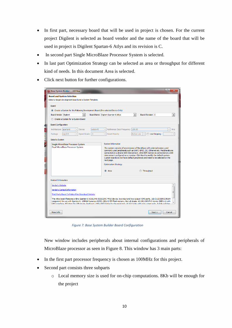
In first part, necessary board that will be used in project is chosen. For the current
project Digilent is selected as board vendor and the name of the board that will be
used in project is Digilent Spartan-6 Atlys and its revision is C.
In second part Single MicroBlaze Processor System is selected.
In last part Optimization Strategy can be selected as area or throughput for different
kind of needs. In this document Area is selected.
Click next button for further configurations.
Figure 7: Base System Builder Board Configuration
New window includes peripherals about internal configurations and peripherals of
MicroBlaze processor as seen in Figure 8. This window has 3 main parts:
In the first part processor frequency is chosen as 100MHz for this project.
Second part consists three subparts
o Local memory size is used for on-chip computations. 8Kb will be enough for
the project

11
o Instruction Cache is used to speed up executable instruction fetch. Frequently
used instructions are stored here. 8Kb will be enough for the project
o Data cache is used to speed up data fetch and store. When processor has to
make a read or write operation it first checks cache lines. If processor finds
corresponding memory in data cache it immediately writes and reads from
that cache line. 8Kb will be enough for the project.
Last part is the place where peripherals of microblaze are selected. In here one can
add or remove the peripherals that will or will not be used in the project. Peripheral
selection is also can be done at next stages. For this project we exclude dip switches,
ethernet lite, leds, push buttons, QSPI flash and rs232 uart modules.
Click finish button to let XPS prepare project for you.
Figure 8: Microprocessor Configuration
After creation of project a sophisticated interface with many features will be
seen. This interface capable of adding new peripherals to MicroBlaze or remove
them, connecting necessary signals to corresponding ports, simulating the project and
exporting the project to the Xilinx SDK tool.

12
Figure 9: Main Interface of XPS
3.2 Attaching AXI Timer
Since AXI System is selected in previous steps we must add AXI timer and AXI
interrupt controller to the project. To add AXI timer, in the IP Catalog section extend
the DMA and Timer, marked as 1 in Figure 9 and in Figure 10, then double click AXI
Timer/Counter peripheral and click yes to question in pop-up window that asks as Do
you want to add one axi_timer 1.03.a IP instance to your design?
Figure 10: AXI Timer
Than XPS core configuration window will be opened. Click the Only One Timer is
present box as marked in Figure 11 then click OK.

13
Figure 11: Core configuration of axi_timer
In next pop-up window named “Instantiate and Connect IP- axi_timer_0”, choose
first option to make bus connections and address assignments automatically. If the
other option is chosen, then necessary confıgurations have to be done manually.
Figure 12: Automatic Wiring Window
3.3 Attaching AXI Interrupt Controller
To add AXI interrupt controller extend Clock, Reset and Interrupt in IP Catalog
section, marked as 2 in Figure 9. Than double click AXI Interrupt Controller
peripheral in Figure 13 and click yes to question in pop-up window that asks as Do
you want to add one axi_timer 1.03.a IP instance to your design?

14
Figure 13: AXI Interrupt Controller
In the IP Core confıguration window there is no need to make any change click OK
to jump further steps. Than in the new pop-up window named “Instantiate and
Connect IP- axi_intc_0”, click first option to automate bus connections and address
assignments same as in the Figure 12.
After adding in IPs, timer interrupts must be connected to interrupt controller and
interrupt controller have to be connected to microblaze interrupt port. To do this
click the System Assembly View, marked as 6 in Figure 9, and then click port
section, marked as 4 in Figure 9. In the new window extend the axi_intc_0 peripheral
and click the L to H: No Confection as shown in Figure 14.
Figure 14: Assigning Timer Interrupt
Than Interrupt connection dialog will pop up as shown in Figure 15. In this dialog
click the axi_timer_0 and blue arrow to add interrupt. Then click ok. This operation
will make necessary changes in system.mhs file.
Figure 15:Interrupt Connection Dialog
15
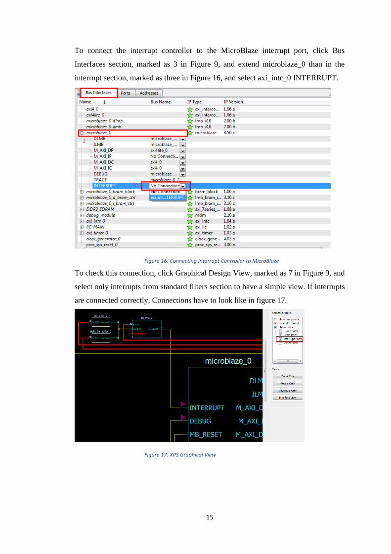
To connect the interrupt controller to the MicroBlaze interrupt port, click Bus
Interfaces section, marked as 3 in Figure 9, and extend microblaze_0 than in the
interrupt section, marked as three in Figure 16, and select axi_intc_0 INTERRUPT.
Figure 16: Connecting Interrupt Controller to MicroBlaze
To check this connection, click Graphical Design View, marked as 7 in Figure 9, and
select only interrupts from standard filters section to have a simple view. If interrupts
are connected correctly, Connections have to look like in figure 17.
Figure 17: XPS Graphical View

16
4. ADDING CUSTOM IP (INTELLECTUAL PROPERTY)
4.1 Creating Barebone Custom IP
In this section, creating a custom hardware will be explained in detail. To create a
brand new custom peripheral, Create or Import Peripheral is selected under the
hardware tab as shown in Figure 18.
Figure 18: Custom IP Creation Menu
Then Create or Import Peripheral Wizard will be opened as in Figure 19. Next button
is clicked to pass information screen. Incoming Create and Import Peripheral Wizard
window consists two parts:
First part is for choosing either creating a new peripheral or importing an existing
one into the project. Create templates for new peripheral option is selected.
Second part is for loading and existing .cip setting file which is created in previous
sections and located at
$(project_path)/pcores/$(name_of_perripheral)/devl/create.cip. All settings will be
done by hand in this document. Therefore, this option is leaved empty.
Next button is clicked for further steps.

17
Figure 19: Create and Import Peripheral Wizard
This step is responsible for selecting project location. If the peripheral that will be
created will be used for other projects too than selecting EDK repository will provide
to access peripheral from other projects automatically. However, if the peripheral is
not suitable for general use, storing peripheral under the project folder is a better
choice. For this project to an XPS project is chosen as shown in Figure 20. Next is
clicked for further steps.
Figure 20:Create Peripheral Window
This step is the place where the name and version of the hardware is specified. Top
module name of the hardware will be same as IP name and it cannot include anything
other than lower case letters decimal digits and underline character. In addition to

18
this, names have to start with a letter and cannot contain underline character at the
end [13]. Version of the hardware also can be selected in this part. Since there was
not and existing version of serial adder, revision is set as default values for this
project and a description can also be added in description box if necessary. Next is
clicked for further steps.
Figure 21: Peripheral Name and Version Configuration
In this step bus interface is chosen. There are 4 different kinds of buses that AXI
system supports. AXI4, AXI4-Lite, AXI4-Stream and Fast Simplex Link (FSL)
AXI4-Lite:
Is a subset of AXI4 interface, it communicates with peripherals over registers in
peripherals. It is a light-weight, single transaction memory mapped interface and
generally used for simple component interface and requires less effort to design.
AXI4-Lite bus is able to work with 32-bit slave configuration, reads and writes with
32-bit data width and supports multiple address ranges [14].
AXI4:
Has a burst mode capability which allows not to verify all the steps of data transfer
and provides higher data throughput. Both AXI4 and AXI4-Lite has 5 channels for
data transfer: read address channel, write address channel, read data channel, write
data channel and write response channel. AXI4 can make up to 256 data transfer per
transaction while AXI4-Lite can only make 1 data transfer. In addition to this AXI4

19
bus supports 32, 64, 128, 256, 512 and 1024 bit data widths while AXI4-Lite only
supports 32 bit [15].
AXI4-Stream:
AXI-Stream is a subset of AXI bus interface which is optimized for high-speed
streaming data. It has only burst mode with selectable input data width between 8-
256 bits [16]. As its name implies, this bus is generally used for real time data
streaming over DVI, HDMI and parallel video sources.
FSL (Fast Simplex Link):
FSL is a uni-directional point-to-point data transfer interface which provides fast data
transfer between peripherals and MicroBlaze core. It builds a one-way point-to-point
data transfer using FIFO(First In First Out) method with supporting FIFO depth
between 1 and 8K, in addition to this, FSL also able to use both synchronous and
asynchronous FIFO modes [17].Since a basic eight bit serial adder will be used in the
project, AXI4-Lite interface is the best choice for current project. Thus AXI4-Lite is
selected as marked in Figure 22 and next is clicked for further steps.
Figure 22: Bus interface Selection
This step is the phase for selecting IPIF (IP Interface) services. It includes two main
sections:
First section provides master service and the configuration which is needed for more
complex peripherals. Since the peripheral that will be going to implemented in this

20
project, is only responsible to add two unsigned integers, there is no need to use
master interface.
Second section provides slave service and configuration which suits the project
needs. It provides three options, software reset, user logic software register and
include data phase timer. This options can be selected for different needs. User logic
software register and include data phase timer is selected for current project as shown
in Figure 23. Next is clicked for further steps.
Figure 23: IP interface configuration
After selecting slave service configuration, if user logic software register is selected
than next step will be the place for selecting number of this registers, otherwise
create peripheral wizard will directly jump to IPIF signal selection step. Although
only two number will be used for adding operation in the custom peripheral, 4
register is needed, 2 for storing input unsigned integers, 1 for start signal and 1 one
for storing the result of summation. Next is clicked for further steps.

21
Figure 24: Software Accessible Register Selection
Next step is the step for the selecting signals between AXI4-Lite and custom
peripheral. These signals are for establishing communication with MicroBlaze over
AXI bus protocol and can be configured according to projects requirements. Default
configuration is used for the current adder project as seen in Figure 25.
Figure 25: IP Interconnect Signals
In next step decision of the BFM simulation is given. Choosing this option will
generate a test bench template, HDL stimulus file for target bus. Generate BFM
simulation platform option is checked for the current project and moved to other
step.
Next phase includes three options which will facilitate the development processes.

22
First option is for selecting the language of “user_logic” file where the actual
peripheral design will be implemented. This option if for the developers that feels
more comfortable while developing with Verilog. Second option generates ISE and
XPS project files to ease development process and the last option is for generating a
basic driver files which will be used wile accessing the hardware from the SDK. All
options are selected as shown in Figure 26 and Next is clicked to pass last step.
Figure 26: Peripheral Implementation Support
Last step summarizes the peripheral features and also shows the place where the
peripheral files are saved. These paths will be used while making adjustments and
adding custom features to IP. Path of the HDL files and ISE project is
C:\Users\Engin\Desktop\microblaze_project\pcores\eight_bit_adder_v1_00_a and
path for the driver files is
C:\Users\Engin\Desktop\microblaze_project\drivers\eight_bit_adder_v1_00_a\src.
Finish is clicked to start the creation of custom peripheral. Newly created IP can be
seen in the IP Catalog under the Project Local PCores as shown in Figure 27.
4.2 Adding Interrupt Port to Custom IP
The aim of the project was decreasing the CPUs burden and enhance the main
process by executing some time consuming operations not on the CPUs internal
cores and registers but process them on peripherals. Thus the only responsibility of

23
the CPU will be to start the operation on peripheral and get the results when the
process ends. By doing so CPU does not have to know how the process is executed
in peripherals. However, there might be different peripherals for different kind of
operations and all these different operations may need different amount of time
which makes these processes asynchronous. Therefore, two different techniques are
used for informing the CPU, polling and interrupt handling. In a polled system, CPU
periodically saves its current state into process stack and asks to peripherals if they
finished their job. If the answer is yes than CPU gets results from peripheral
otherwise continues its previous process. As it is seen this approach is not very
efficient due to no answers. However, with an interrupt based system both CPU and
peripheral has an extra port for interrupt signal. Thereby whenever one peripheral
finishes its job, it sends a signal to this port and gets attention of the CPU. As soon as
CPU senses an interrupt it saves the current state of the process into stack and take
cares of the peripheral outputs.
Since MicroBlaze support interrupt driven processes and has one interrupt port, to
connect eight bit adder IP to MicroBlaze, an interrupt controller have to be used and
interrupt port have to be added to the adder peripheral. While creation of the
peripheral, corresponding ISE project were also created and can be found under the
project files. For adding an extra output port, necessary changes must be done on
“user_logic.v” file in the ISE project. Path of the “user_logic.v” for current project is
C:\Users\Engin\Desktop\microblaze_project\pcores\eight_bit_adder_v1_00_a\devl\p
rojnav
After opening the ISE project “user_logic.v” file is opened and extra output is added
as shown in Figure 28 and Figure 29. Since this port will be used as interrupt port, its
name is selected consistently.
Figure 28: Adding Extra Port to Custom IP
24
Figure 29: Defining Extra Port
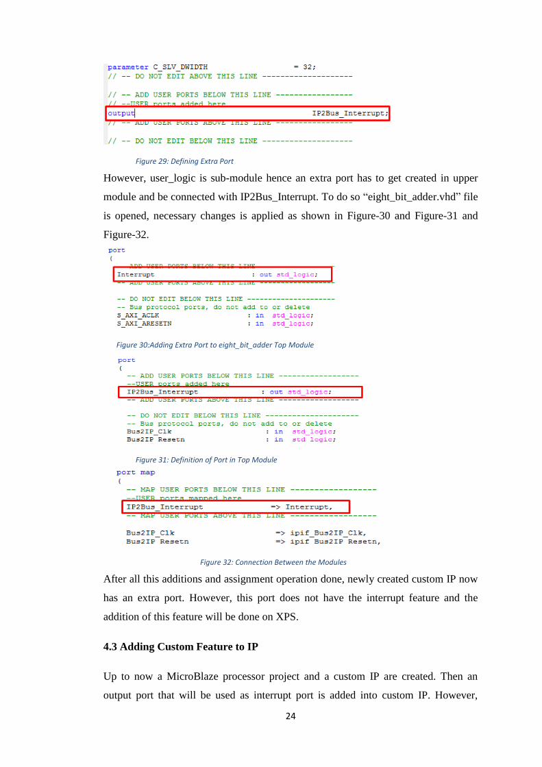
However, user_logic is sub-module hence an extra port has to get created in upper
module and be connected with IP2Bus_Interrupt. To do so “eight_bit_adder.vhd” file
is opened, necessary changes is applied as shown in Figure-30 and Figure-31 and
Figure-32.
Figure 30:Adding Extra Port to eight_bit_adder Top Module
Figure 31: Definition of Port in Top Module
Figure 32: Connection Between the Modules
After all this additions and assignment operation done, newly created custom IP now
has an extra port. However, this port does not have the interrupt feature and the
addition of this feature will be done on XPS.
4.3 Adding Custom Feature to IP
Up to now a MicroBlaze processor project and a custom IP are created. Then an
output port that will be used as interrupt port is added into custom IP. However,

25
Custom IP still does not have any special feature. This feature can be designed in a
separate Verilog file and added into user_logic file as a submodule. In the current
project an 8 bit serial adder will be designed and implemented into custom IP.
4.3.1 Design the Serial Adder
Serial adder module adds two unsigned eight-bit integers and return the sum in
eight-bit for simplicity overflow conditions does not considered. In attempt to realize
this, five input and two output ports are added into adder. Input ports are first
number(a), second number(b), clock signal(clk), reset(rst) signal and start(start)
signal respectively. Output ports are sum(c) and done(done) signal. When start signal
is triggered adder algorithm will start to run for nine cycles and at the end of 9th
clock cycle sum of two inputs will be assigned to output port and done signal will be
set high for 1 clock cycle. Adding algorithm is based on shifting bits on local
registers, at each cycle least significant bits of inputs are summed with a full adder
and result is written into most significant bit of local sum register. Than all register
contents is shifted to one bit left. This process is repeated for eight clock cycles and
at the ninth clock signal results are assigned to corresponding ports. External view of
the SerialAdder module is shown in Figure 33.
4.3.2 Implementation of Serial Adder into IP
To implement adder functionality into newly created peripheral, pre-established
SerialAdder.v file is copied into Verilog folder. Path of this folder is
C:\Users\Engin\Desktop\microblaze_project\pcores\eight_bit_adder_v1_00_a\hdl\ve
rilog for the current project. Than eight_bit_adder_v2_1_0.pao file is opened and
SerialAdder module is linked up in the file as shown in Figure 34 then .pao" “file is
saved and closed. This step is crucial for introducing serial adder module to XPS, if it
is not done properly than “SerialAdder is black box” error will occur. Path of the
eight_bit_adder_v2_1_0.pao for the current project is
C:\Users\Engin\Desktop\microblaze_project\pcores\eight_bit_adder_v1_00_a\data.

26
Figure 34: .pao file of IP
After introducing adder module to XPS, this module has to be mounted in
user_logic file. To do so ISE project for the corresponding IP is opened under the
projnav folder. Path of this folder in current project is
C:\Users\Engin\Desktop\microblaze_project\pcores\eight_bit_adder_v1_00_a\devl\p
rojnav. Then SerialAdder,v file is imported into ISE project as show in Figure 35.
Figure 35: Addition of SerialAdder.v
Than user_logic.v is opened and two wires is defined as seen in Figure 36, one for
result of summation and one for done signal that indicates the end of summation
operation.
Figure 36: Net Declarations

27
Than an adder instance “SA” is created and necessary input/output variables are
placed in the SA as shown in Figure 37.
First slave register will hold first number in its first eight bit.
Second slave register will hold second number in its first eight bit.
Clock and reset signals of serial adder will be same as IPs clock and reset
signals
Third slave register will hold start signal in its first bit
Last slave register will hold the sum of first two inputs after summation
process ends.
Done signal will be used as interrupt to inform the MicroBlaze
Figure 37: Submodule Decleration
Code for write operation from bus to registers is came by default. As the summation
result will be written into fourth register (slv_reg3), there should not be any write
operation from bus to forth register. For this reason, write operation for slv_reg3 is
commented as shown in Figure 38 and Figure 39. Assignment operation is done just
before the case statement. Hence assignment will be done in every clock cycle.
Figure 38:Assignment of Output

28
Figure 39:Commenting Third Register
As it mentioned while design of serial adder, when summation operation is finished
in SerialAdder module, done signal will be set high for one clock cycle. This signal
is assigned to Interrupt port of custom peripheral to inform the MicroBlaze processor
as shown in Figure 40. The complete HDL code is added to Appendix-A.
Figure 40: Assign Done Signal to Interrupt Port
4.3 Connecting Custom IP to Interrupt Controller
In the main window of XPS, newly created custom IP is right clicked and view MDP
(Microprocessor Peripheral Definition) option is selected. After this selection
“eight_bit_adder_v2_1_0.mpd file is opened. This file describes the interface for the
custom IP and has sections where ports, connections for bus interface and parameter
list were listed [18]. In the file under the port section a new port has to be added with
special keywords and the same name in the “eight_bit_adder.vhd” file. For the
current project marked line in the below Figure 41 is added.
Figure 41: Interrupt Port Definition in MPD File
Here the route of the signal is assigned with DIR attribute which accept three
different options “I” for input, “O” for output and “IO” for both [19].
The kind of the signal is defined by the SIGIS attribute which can take 3 kind of
options CLK for clock signals INTERRUPT for interrupt signals and RST for reset
signals [19]. The decision of the time when the interrupt signal will be set high is

29
arranged with the SENSİTİVİTY keyword which is able to take for parameters,
EDGE_FALLING, EDGE_RISING, LEVEL_HIGH or LEVEL_LOW [19]. Relative
priority of the interrupt signal can be assigned with the INTERRUPT_ PRIORITY
keyword which can be set as HIGH, MEDIUM and LOW options [19]. Decision of
this relative priority is given by the designer of the custom peripheral with taking the
consideration of byte-rate of IP. Since the current project does not work with
extremely high or extremely low speeds MEDİUM priority will suits the project
needs. After addition of the new port into MPD file, for connecting the interrupt port
of IP to the interrupt controller firstly user repositories is rescanned from Project-
>Rescan User Repositories in main XPS window as shown in Figure 42.
Figure 42: Rescan User Repositories
Then EIGHT_BIT_ADDER peripheral is right clicked from the IP Catalog section
and Add IP option is selected as shown below Figure 43 and yes is clicked as
response to pop-up window.
Figure 43: Adding Custom IP to Project
Then configuration window will pop-up, necessary changes can be done from this
window. Since 4 register is used for the current project, number of the registers
“C_NUM_REG” is increased to 4 as shown in Figure 44. After doing this ok button
is clicked and in further step, automatic binding option is selected as in the previous
steps.

30
Figure 44: Assign Number of Register
Now custom IP is added and connected to the AXI4-Lite bus and it is time to
connect Interrupt port to the axi_intc_0 peripheral. To accomplish this, Port tab is
clicked under the System Assembly View and eight_bit_adder IP is expanded.
Interrupt port of the adder might be seen with a little pen icon near it in this step,
click it to open interrupt connection dialog. If not so, try to rescan user repositories as
explained above and re-add the custom IP after removing the old one from the
project. Custom IP is selected with the corresponding port name and added to
interrupt list by clicking blue arrow in the middle of the Interrupt Connection Dialog
as shown in Figure 45. Interrupt Connection Dialog can be open directly by clicking
INT button pointed by a red arrow in Figure 46.
Figure 45: Attaching Adder to Interrupt List
31
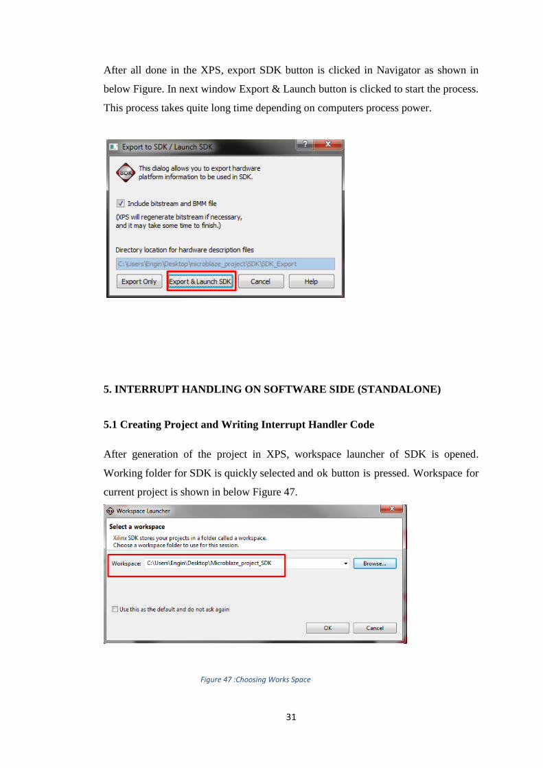
After all done in the XPS, export SDK button is clicked in Navigator as shown in
below Figure. In next window Export & Launch button is clicked to start the process.
This process takes quite long time depending on computers process power.
5. INTERRUPT HANDLING ON SOFTWARE SIDE (STANDALONE)
5.1 Creating Project and Writing Interrupt Handler Code
After generation of the project in XPS, workspace launcher of SDK is opened.
Working folder for SDK is quickly selected and ok button is pressed. Workspace for
current project is shown in below Figure 47.
Figure 47 :Choosing Works Space

32
Before going to create an application project, driver files for the custom IP have to
get introduced. To do this Xilinx Tools->repositories is selected as in Figure 48.
Figure 48: Adding Repositories (a)
Path of the driver files could be added as global or local repository. If they added as
global repository than all projects will be able to access this files without adding
them every time. If they added locally than only the current project will be able to
access driver files. For the current project new button at right side of local
repositories is clicked and path of the XPS project is added as shown in Figure 49.
Project path for current project is C:\Users\Engin\Desktop\microblaze_project
Figure 49: Adding Repositories (b)
After introducing driver files new application project is created from file->New-
>New Application Project at upper left side of main SDK window as shown in below
Figure 50.
Figure 50: Application Project Creation
Then project wizard will be opened. Here there is no need to change anything except
writing the project name. Hardware platform stays in its default value which is

33
already created by XPS in previous steps. MicroBlaze processor also has to stay
same since we used it in previous steps. OS platform can be chosen as standalone,
Xilkernel or Linux. In the current project standalone is selected. Since Board Support
package is not existing, a new one have to be created. Then next is clicked to pass
next step as.
Figure 51: Create Project Wizard
In this step Hello world project is selected as reference. Then the project code will be
implemented instead of hello world file. Then finish button is clicked to start
creation of SDK project. While the project is buit automatically it gives an error
because number of registers is defined different in hearder file and test file. To
correct this both header file and test file is opened with an external text editor. At the
bottom of header file number of register is defined as
#define TEST_AXI_LITE_USER_NUM_REG 4 however it is used with different
name in test file as shown in Figure 52. TEST_AXI_LITE_USER_NUM_REG
constans is replaced with the constant in header file.

34
Figure 52: Correct Error in Test File
Than the name of the helloword file is changed, print statement is deleted and project
is builded again. There is some useful example codes about how to use custom IP
drivers in the source folders of IPs. Path of the interrupt controler examples for the
current project is
E:\Xilinx_EDK\14.7\ISE_DS\EDK\sw\XilinxProcessorIPLib\drivers\intc_v2_06_a\ex
amples. This example is tailored for needs of the serial adder project and editted code
is added into Appendix-B.
5.2 Running Project on Digilent Atlys Spartan-6 Board
For running the cone on real hardware, two micro usb cable is attached PROG and
UART port of the board and charger is plugged the board. Then in SDK Xilinx
Tools->Configure JTAG settings is selected as choesn in Figure 53(a).
Figure 53: JTAG Configuration (a)
Then from the incoming Configure JTAG window, Digilet USB Cable is selected as
in Figure 54.

35
Figure 54: Jtag Configuration (b)
Then from Xilinx Tool->Program FPGA from the main screen as shown below
figure. Now it is time to run C program on hardware. To see the results on console ,
Run->Run Configurations is selecter from the main menu tool bar. As shown in
Figure 55.
Figure 55: Run configuration (a)
After this, SerialAdder configuration selected and STDIO connection tab is clicked.
Under this tab connect STDIO to console box is marked, corresponding port is
selected for data transfer from board to console and apply is selected. For the current
project port 4 is selected as shown in Figure 56.

36
Figure 56: STDIO in Console
Then SerialAdder is right clicked from Project Explorer and Generate Linker Script
is selected. As shown in Figure 57(a).
Figure 57: Generate Linker Script (a)
After this in the incoming window under the basic tab, Place Code Sections, place
Data Sections, Place Heap and Stack is assigned to
ddr3_sdram_S_AXI_BASEADDR.

37
Figure 58: Generate Linker Script (b)
In last step project is built and installed to board after selecting Launch on Hardware is in
Figure 59. Results will be seen in console if STDIO configuration is done correctly.
Figure 59: Run Project on Board

38
References
[1] UK Essays. November 2013. Fpga Vs Cpld. [online]. Available from:
http://www.ukessays.co.uk/essays/communications/fpga-vs-cpld.php?cref=1
[Accessed 17 May 2016].
[2] "Scribd," Scribd, [Online]. Available: https://tr.scribd.com/doc/20477704/Hardware-
Description-Language-HDL-Introduction-to-HDL. [Accessed 15 5 2016].
[3] M. Rouse, "Whatls," TechTarget, 3 2010. [Online]. Available:
http://whatis.techtarget.com/definition/EEPROM-electrically-erasable-programmable-
read-only-memory. [Accessed 15 5 2016].
[4] "Xilinx," Xilinx Inc., [Online]. Available: http://www.xilinx.com/products/design-
tools/microblaze.html . [Accessed 13 05 2016].
[5] "PennState," The Pennsylvania State University, 20 2 2010. [Online]. Available:
http://ecse.bd.psu.edu/cenbd452/lecture/lecture17.html. [Accessed 12 5 2016].
[6] "Xilinx," Xilinx Inc, [Online]. Available: http://www.xilinx.com/products/intellectual-
property/plb_v46.html. [Accessed 13 5 2015].
[7] "AXI Interconnect," Xilinx Inc, [Online]. Available:
http://www.xilinx.com/products/intellectual-property/axi_interconnect.html.
[Accessed 2012 5 2016].
[8] "Electronic Design," Penton Corporate, 5 3 2001. [Online]. Available:
http://electronicdesign.com/microprocessors/advanced-microprocessor-bus-
architecture-amba-bus-system. [Accessed 12 5 2016].
[9] "AXI Reference Guide," 7 3 2011. [Online]. Available:
http://www.xilinx.com/support/documentation/ip_documentation/ug761_axi_refere

39
nce_guide.pdf. [Accessed 13 5 2016].
[10] "Xilinx," Xilinx Inc, [Online]. Available: http://www.xilinx.com/products/design-
tools/xps.html. [Accessed 13 5 2016].
[11] "Xilinx," Xilinx Inc, [Online]. Available: http://www.xilinx.com/products/design-
tools/ise-design-suite.html. [Accessed 13 5 2016].
[12] "Xilinx Software Development Kit Help Contents," Xilinx Inc, [Online]. Available:
http://www.xilinx.com/support/documentation/sw_manuals/xilinx2014_3/SDK_Doc/i
ndex.html. [Accessed 14 5 2016].
[13] "Xilinx," Xilinx Inc, 2008. [Online]. Available:
http://www.xilinx.com/itp/xilinx10/help/platform_studio/ps_r_ipw_peripheral_namin
g_conventions.htm. [Accessed 15 5 2016].
[14] xilinx, "LogiCORE IP AXI4-Lite IPIF v2.0," 18 12 2008. [Online]. Available:
http://www.xilinx.com/support/documentation/ip_documentation/axi_lite_ipif/v2_0/
pg155-axi-lite-ipif.pdf. [Accessed 14 5 2016].
[15] Xilinx, "AXI Referance Guide," 18 1 2012. [Online]. Available:
http://www.xilinx.com/support/documentation/ip_documentation/axi_ref_guide/v13
_4/ug761_axi_reference_guide.pdf. [Accessed 15 5 2016].
[16] Xilinx, "LogiCORE IP Video In to AXI4-Stream v3.0," 2 4 2014. [Online]. Available:
http://www.xilinx.com/support/documentation/ip_documentation/v_vid_in_axi4s/v3
_0/pg043_v_vid_in_axi4s.pdf. [Accessed 15 5 2016].
[17] Xilinx Inc, "LogiCore IP Fast Simplex Link v20 Bus," 19 4 2010. [Online]. Available:
http://www.xilinx.com/support/documentation/ip_documentation/fsl_v20.pdf.
[Accessed 15 5 2016].
[18] Xilinx, Xilinx Inc, 2008. [Online]. Available:
http://www.xilinx.com/itp/xilinx10/help/platform_studio/ps_r_gst_project_files.htm.
[Accessed 16 5 2016].
[19] Xilinx Inc, "Platform Specification Format," 2008. [Online]. Available:
http://www.xilinx.com/support/documentation/sw_manuals/edk10_psf_rm.pdf.
[Accessed 16 5 2016].

40
Appendix-A
Codes will be added after correction.
SerialAdder.v
user_logic.v
eight_bit_adder.vhd
Appendix-B
Codes will be added after correction.
SerialAdder.c