istanbul technical university electrical – electronics engineering faculty implementation of...
TRANSCRIPT
1
ISTANBUL TECHNICAL UNIVERSITY
ELECTRICAL – ELECTRONICS ENGINEERING FACULTY
IMPLEMENTATION of SECURE HASH ALGORITHM on FIELD PROGRAMMABLE GATE ARRAY
BSc Thesis by
Oğuz YELBEY
040040367
Department: Electronics and Communication Engineering
Programme: Electronics Engineering
Supervisor : Assis. Prof. Dr. Sıddıka Berna Örs Yalçın
MAY 2010

2
FOREWORD
I would like to thank my supervisors Assis. Prof. Dr Sıddıka Berna Örs Yalçın and Assis.
Prof. Dr Gökay Saldamlı. Without their help this work would not have been possible.
May 2010 Oğuz Yelbey
3
TABLE of CONTENTS
ÖZET v
SUMMARY vi
1. INTRODUCTION 1
2. SECURE HASH ALGORITHM-1 2
2.1. Appending Padding Bits 2
2.2. Appending Length 2
2.3. Initialization of Default Hash Values 2
2.4. Processing of the message 3
3. GROESTL-256 ALGORITHM 6
3.1. The Hash Function Construction 6
3.2. The Compression Function Construction 6
3.3. The Output Transformation 7
3.4. The Design of P and Q 8
3.5. Mapping From a Byte Sequence to a State Matrix 9
3.6. Add Round Constant 10
3.7. Sub Bytes 11
3.8. Shift Bytes 12
3.9. Mix Bytes 12
3.10. Number of rounds 14
3.11. Initial value 14
3.12. Padding 14
3.13. Summary 15
4. IMPLEMENTATION of SECURE HASH ALGORITHM-1 on FPGA 16
4.1. Architecture of the Overall System 16
4.2. Architecture and Operation of the SHA-1 Module 18
4.3. Architecture of the “Calculate Digest” Module 19
4.4. Operation of the SHA-1 Module With CPU 20
4.5. Simulation of the Implemented Design 21

4
5. IMPLEMENTATION of GROESTL-256 on FPGA 24
5.1. Implementation of Add Round Constant 24
5.2. Implementation of Sub Bytes 24
5.3. Implementation of Shift Bytes 25
5.4. Implementation of Mix Bytes 25
5.5. Construction of One Round 26
5.6. Complete Groestl-256 System 27
5.7. Simulation of Groestl-256 Implementation 29
6. RESULTS and DISCUSSION 31
REFERENCES 32
APPENDIX A 33
APPENDIX B 34
AUTOBIOGRAPHY 38
5
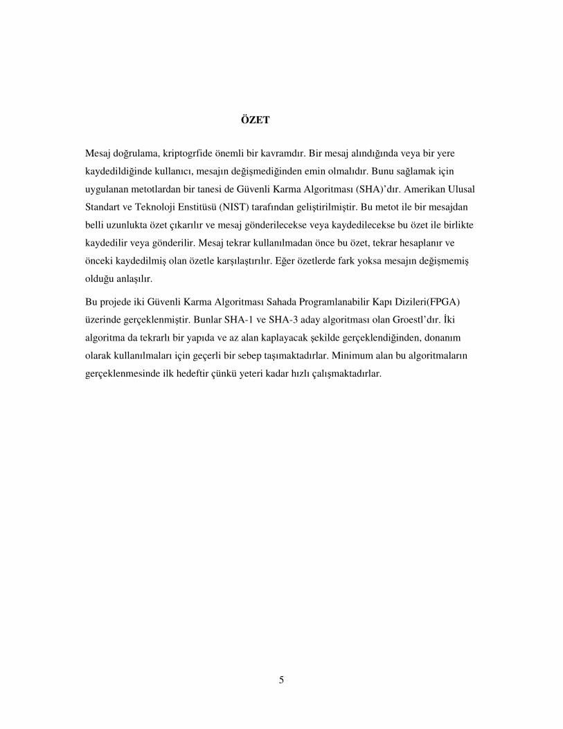
ÖZET
Mesaj doğrulama, kriptogrfide önemli bir kavramdır. Bir mesaj alındığında veya bir yere
kaydedildiğinde kullanıcı, mesajın değişmediğinden emin olmalıdır. Bunu sağlamak için
uygulanan metotlardan bir tanesi de Güvenli Karma Algoritması (SHA)’dır. Amerikan Ulusal
Standart ve Teknoloji Enstitüsü (NIST) tarafından geliştirilmiştir. Bu metot ile bir mesajdan
belli uzunlukta özet çıkarılır ve mesaj gönderilecekse veya kaydedilecekse bu özet ile birlikte
kaydedilir veya gönderilir. Mesaj tekrar kullanılmadan önce bu özet, tekrar hesaplanır ve
önceki kaydedilmiş olan özetle karşılaştırılır. Eğer özetlerde fark yoksa mesajın değişmemiş
olduğu anlaşılır.
Bu projede iki Güvenli Karma Algoritması Sahada Programlanabilir Kapı Dizileri(FPGA)
üzerinde gerçeklenmiştir. Bunlar SHA-1 ve SHA-3 aday algoritması olan Groestl’dır. Đki
algoritma da tekrarlı bir yapıda ve az alan kaplayacak şekilde gerçeklendiğinden, donanım
olarak kullanılmaları için geçerli bir sebep taşımaktadırlar. Minimum alan bu algoritmaların
gerçeklenmesinde ilk hedeftir çünkü yeteri kadar hızlı çalışmaktadırlar.

6
SUMMARY
Message integrity is one of the most important subjects in cryptography. When a message is
received or stored in a location, user must be sure that message is not changed. To be able to
accomplish this message integrity, one of the methods is Secure Hash Algorithm (SHA),
which is being published by National Institute of Standards and Technology (NIST). In this
method, a message digest is produced from a message and message is sent or stored in a
location with its digest. Before the message is used, the digest is produced again. If there is a
difference in the message, the digest is changes also. Otherwise the message is not changed
and reliable to be used.
In this project, two SHA algorithms are implemented on Field Programmable Gate Array
(FPGA) which are SHA-1 and SHA-3 candidate algorithm called Groestl. Because of their
recursive structure, both of the algorithms are reasonable to be used for hardware
implementations. The main consideration of these implementations is minimum area because
they’re fast enough to use on most applications. Also, area means cost and low cost is mostly
first consideration of most applications.
7
1. INTRODUCTION
There are several versions of SHA. The three SHA algorithms are structured differently and
are distinguished as SHA-0, SHA-1, and SHA-2. The SHA-2 family uses an identical
algorithm with a variable digest size which is distinguished as SHA-224, SHA-256, SHA-
384, and SHA-512[1]. SHA-3 is not published as a standard but there is a competition for
that. 12 candidate algorithms are distinguished so far. One of them is Groestl, which is used to
be implemented on this project.
Algorithm may be implemented as hardware or software. All of them have advantages and
disadvantages. Software implementations cannot provide desired throughput for high-speed
systems such as video transmission systems. However, hardware implementations are
expensive and change in algorithm means a new hardware. Because of this reason,
reconfigurable hardware is commonly used for hash functions such as FPGA.
In the following, algorithms that are used in project will be explained. Then implemented
algorithms on FPGA will be described and two of them will be compared on their area
requirements and speed.

8
2. SECURE HASH ALGORITHM-1
The SHA-1 consists of the following steps:
2.1. Appending Padding Bits
The b-bit M is padded as follows: a single 1-bit is added into the end of M, after which 0-bits
are added until the length of the message is equivalent to 448, modulo 512[1].
2.2. Appending Length
After message is padded, 64 bit representation of b is added to the end of the padded message
so that message length becomes multiple of 512 bits [1].
2.3. Initialization of Default Hash Values
Let , , , , ,be 32-bit hash value registers. These registers are used in the
derivation of a 160-bit hash H. At the beginning, they are initialized as follows [1]:
= x′′67452301′′
= x′′efcdab89′′
= x′′98badcfe′′ (2.1)
= x′′10325476′′
= x′′c3d2e1f0′′

9
2.4. Processing of the message
The algorithm which is used for processing of the padded message is explained next. First, the
padded message needs to be divided into 512-bit blocks, denoted here as Mj where j ≥ 0 is the
index of the block. The algorithm processes one Mj at once, starting from M0, until all Mj
have been processed. Five 32-bit registers, A, B, C, D and E are defined for algorithm. At the
beginning of processing of each Mj their values are set as follows: A←H0, B←H1, etc. The
algorithm consists of 80 steps. Let t denote the index of a step, i.e. 0 ≤t ≤ 79. First, a 32-bit
message block Wt is derived for every step t from the 512-bit message block Mj using a
message schedule. For t < 16, Wt is simply the t.th 32-bit word of Mj. When t ≥ 16, Wt are
derived recursively with the following formula:
Wt = (Wt−3 ⊕Wt−8 ⊕Wt−14 ⊕Wt−16) ≪1 (2.2)
Where ≪ denotes circular shift to the left by s bits and ⊕ is a logical xor-operation. Let Kt be
a constant value for step t. The values of K are set as follows:
x′′5a827999′′ 0 ≤ t ≤ 19
x′′6ed9eba1′′ 20 ≤ t ≤ 39
x′′8fbbcdc′′ 40 ≤ t ≤ 49
x′′ca62c1d6′′ 50 ≤ t ≤ 79
2.3)
10
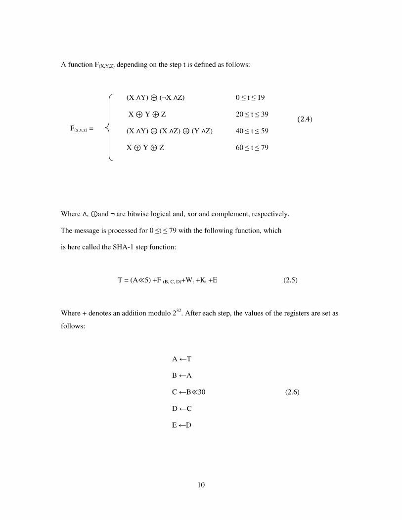
A function F(X,Y,Z) depending on the step t is defined as follows:
(X ∧Y) ⊕ (¬X ∧Z) 0 ≤ t ≤ 19
X ⊕ Y ⊕ Z 20 ≤ t ≤ 39
(X ∧Y) ⊕ (X ∧Z) ⊕ (Y ∧Z) 40 ≤ t ≤ 59
X ⊕ Y ⊕ Z 60 ≤ t ≤ 79
Where ∧, ⊕and ¬ are bitwise logical and, xor and complement, respectively.
The message is processed for 0 ≤t ≤ 79 with the following function, which
is here called the SHA-1 step function:
T = (A≪5) +F (B, C, D)+Wt +Kt +E (2.5)
Where + denotes an addition modulo 232. After each step, the values of the registers are set as
follows:
A ←T
B ←A
C ←B≪30 (2.6)
D ←C
E ←D
2.4)
F(x,y,z) =
11
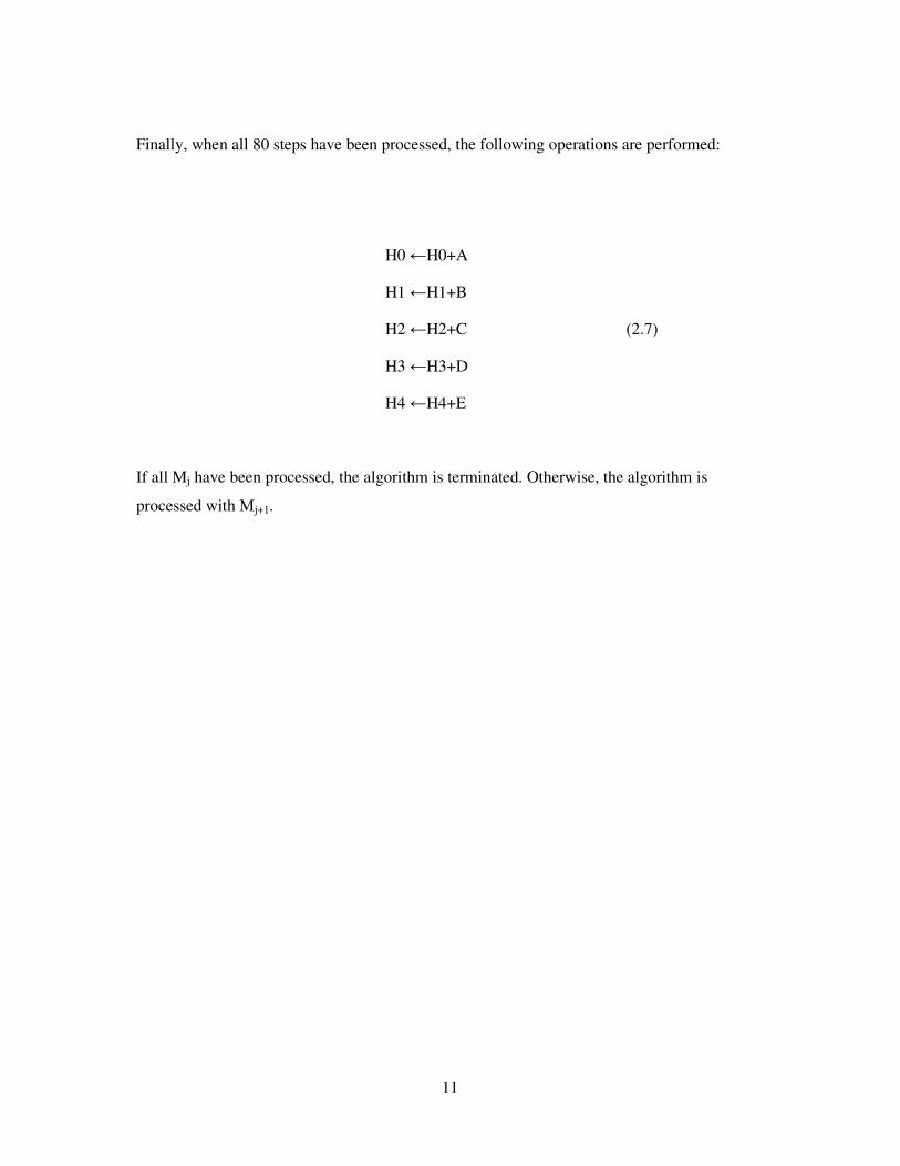
Finally, when all 80 steps have been processed, the following operations are performed:
H0 ←H0+A
H1 ←H1+B
H2 ←H2+C (2.7)
H3 ←H3+D
H4 ←H4+E
If all Mj have been processed, the algorithm is terminated. Otherwise, the algorithm is
processed with Mj+1.
12
3. GROESTL-256 ALGORITHM
3.1. The Hash Function Construction
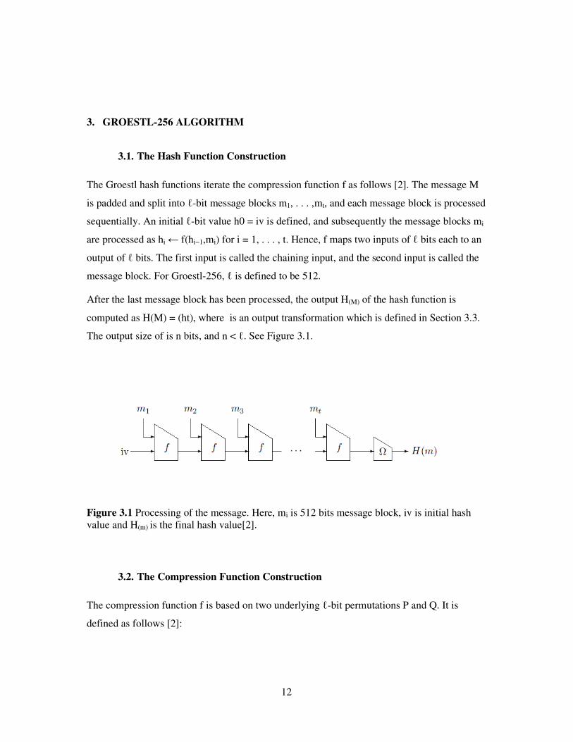
The Groestl hash functions iterate the compression function f as follows [2]. The message M
is padded and split into ℓ-bit message blocks m1, . . . ,mt, and each message block is processed
sequentially. An initial ℓ-bit value h0 = iv is defined, and subsequently the message blocks mi
are processed as hi ← f(hi−1,mi) for i = 1, . . . , t. Hence, f maps two inputs of ℓ bits each to an
output of ℓ bits. The first input is called the chaining input, and the second input is called the
message block. For Groestl-256, ℓ is defined to be 512.
After the last message block has been processed, the output H(M) of the hash function is
computed as H(M) = (ht), where is an output transformation which is defined in Section 3.3.
The output size of is n bits, and n < ℓ. See Figure 3.1.
Figure 3.1 Processing of the message. Here, mi is 512 bits message block, iv is initial hash value and H(m) is the final hash value[2].
3.2. The Compression Function Construction
The compression function f is based on two underlying ℓ-bit permutations P and Q. It is
defined as follows [2]:

13
f(h,m) = P(h ⊕ m) ⊕ Q(m) ⊕ h. (3.1)
The construction of f is illustrated in Figure 3.2. In Section 3.4, P and Q are explained.
Figure 3.2 Function f. Here, ⊕ is bitwise logical xor operation.
3.3. The Output Transformation
Output transformation is illustrated in Figure 3.3. Let truncn(x) be the operation that discards
all but the trailing n bits of x. Then the output transformation is defined as
Ω(x) = truncn(P(x) ⊕ x). (3.2)

14
Figure 3.3 Output transformation. Here, ⊕ is bitwise logical xor operation. Block in the most right is truncn(x) which is described in equation (3.2)[2].
3.4. The Design of P and Q
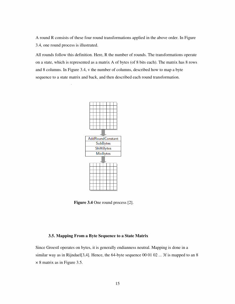
The design of P and Q was inspired by the Rijndael block cipher algorithm [3, 4]. This means
that their design consist of a number of rounds R, which consists of a number of round
transformations. Since P and Q are much larger than the 128-bit state size of Rijndael, most
round transformations have been redefined. In Groestl, a total of four round transformations
are defined for each permutation. These are
• AddRoundConstant
• SubBytes
• ShiftBytes
• MixBytes.
Hence,
R = MixBytes ShiftBytes SubBytes AddRoundConstant. (3.3)
15
A round R consists of these four round transformations applied in the above order. In Figure
3.4, one round process is illustrated.
All rounds follow this definition. Here, R the number of rounds. The transformations operate
on a state, which is represented as a matrix A of bytes (of 8 bits each). The matrix has 8 rows
and 8 columns. In Figure 3.4, v the number of columns, described how to map a byte
sequence to a state matrix and back, and then described each round transformation.
Figure 3.4 One round process [2].
3.5. Mapping From a Byte Sequence to a State Matrix
Since Groestl operates on bytes, it is generally endianness neutral. Mapping is done in a
similar way as in Rijndael[3,4]. Hence, the 64-byte sequence 00 01 02 ... 3f is mapped to an 8
× 8 matrix as in Figure 3.5.
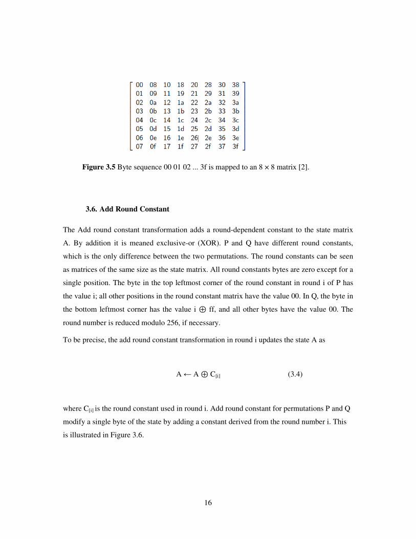
16
Figure 3.5 Byte sequence 00 01 02 ... 3f is mapped to an 8 × 8 matrix [2].
3.6. Add Round Constant
The Add round constant transformation adds a round-dependent constant to the state matrix
A. By addition it is meaned exclusive-or (XOR). P and Q have different round constants,
which is the only difference between the two permutations. The round constants can be seen
as matrices of the same size as the state matrix. All round constants bytes are zero except for a
single position. The byte in the top leftmost corner of the round constant in round i of P has
the value i; all other positions in the round constant matrix have the value 00. In Q, the byte in
the bottom leftmost corner has the value i ⊕ ff, and all other bytes have the value 00. The
round number is reduced modulo 256, if necessary.
To be precise, the add round constant transformation in round i updates the state A as
A ← A ⊕ C[i] (3.4)
where C[i] is the round constant used in round i. Add round constant for permutations P and Q
modify a single byte of the state by adding a constant derived from the round number i. This
is illustrated in Figure 3.6.
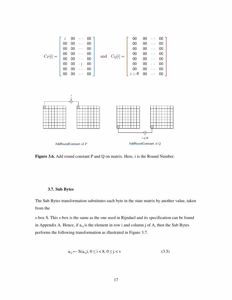
17
Figure 3.6. Add round constant P and Q on matrix. Here, i is the Round Number.
3.7. Sub Bytes
The Sub Bytes transformation substitutes each byte in the state matrix by another value, taken
from the
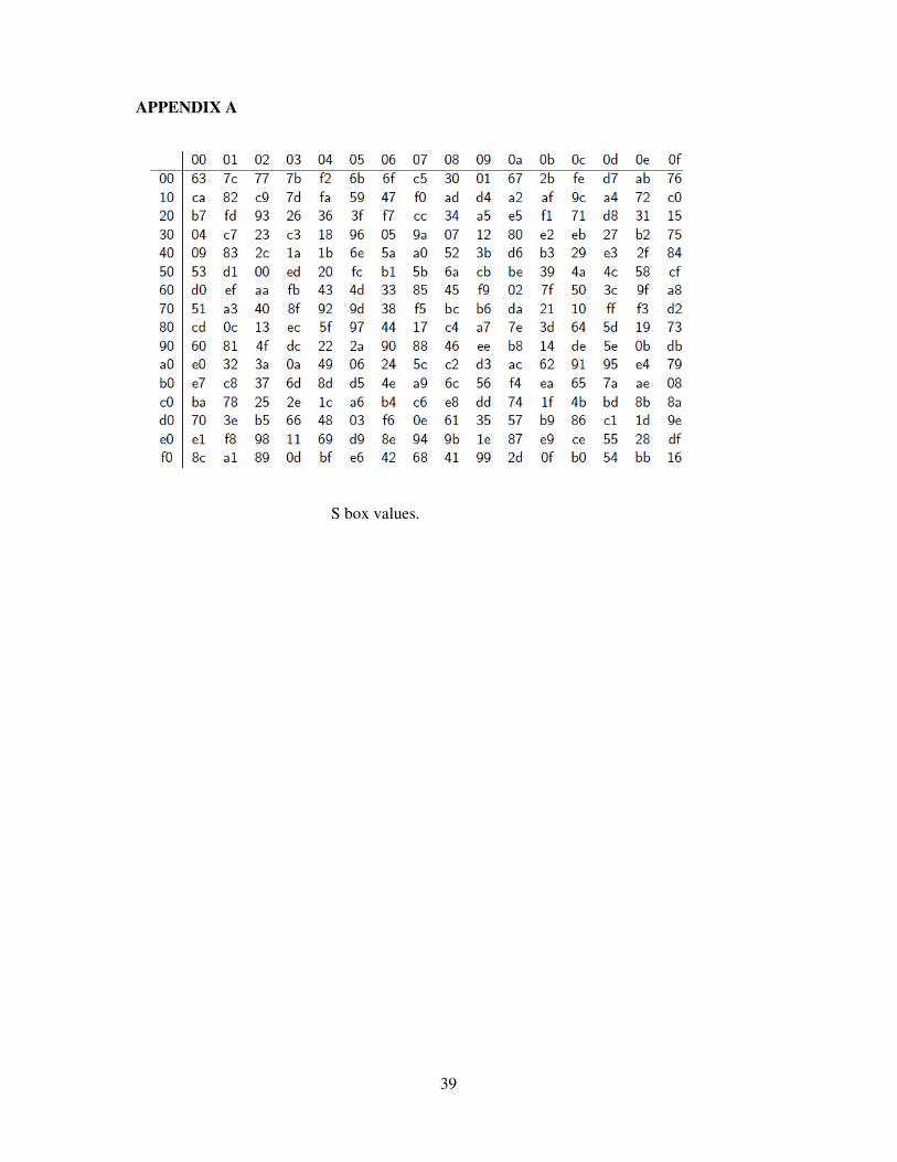
s-box S. This s-box is the same as the one used in Rijndael and its specification can be found
in Appendix A. Hence, if ai,j is the element in row i and column j of A, then the Sub Bytes
performs the following transformation as illustrated in Figure 3.7.
ai,j ← S(ai,j), 0 ≤ i < 8, 0 ≤ j < v (3.5)

18
Figure 3.7 Sub bytes substitutes each byte of the state by its image under the s-box.
3.8. Shift Bytes
Shift bytes cyclically shift the bytes within a row to the left by a number of positions. Let σ =
[σ0, σ1, . . . , σ7] be a list of distinct integers in the range from 0 to v − 1.
Then, ShiftBytes moves all bytes in row i of the state matrix σi positions to the left, wrapping
around as necessary. The vector σ is defined as σ = [0, 1, 2, 3, 4, 5, 6, 7]. In Figure 3.8, this
process is illustrated.
Figure 3.8. The Shift Bytes transformation.
19
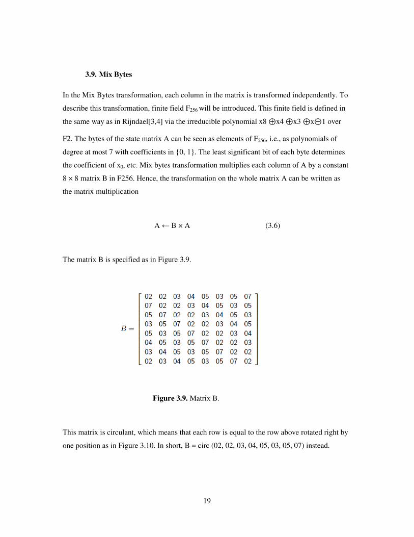
3.9. Mix Bytes
In the Mix Bytes transformation, each column in the matrix is transformed independently. To
describe this transformation, finite field F256 will be introduced. This finite field is defined in
the same way as in Rijndael[3,4] via the irreducible polynomial x8 ⊕x4 ⊕x3 ⊕x⊕1 over
F2. The bytes of the state matrix A can be seen as elements of F256, i.e., as polynomials of
degree at most 7 with coefficients in 0, 1. The least significant bit of each byte determines
the coefficient of x0, etc. Mix bytes transformation multiplies each column of A by a constant
8 × 8 matrix B in F256. Hence, the transformation on the whole matrix A can be written as
the matrix multiplication
A ← B × A (3.6)
The matrix B is specified as in Figure 3.9.
Figure 3.9. Matrix B.
This matrix is circulant, which means that each row is equal to the row above rotated right by
one position as in Figure 3.10. In short, B = circ (02, 02, 03, 04, 05, 03, 05, 07) instead.
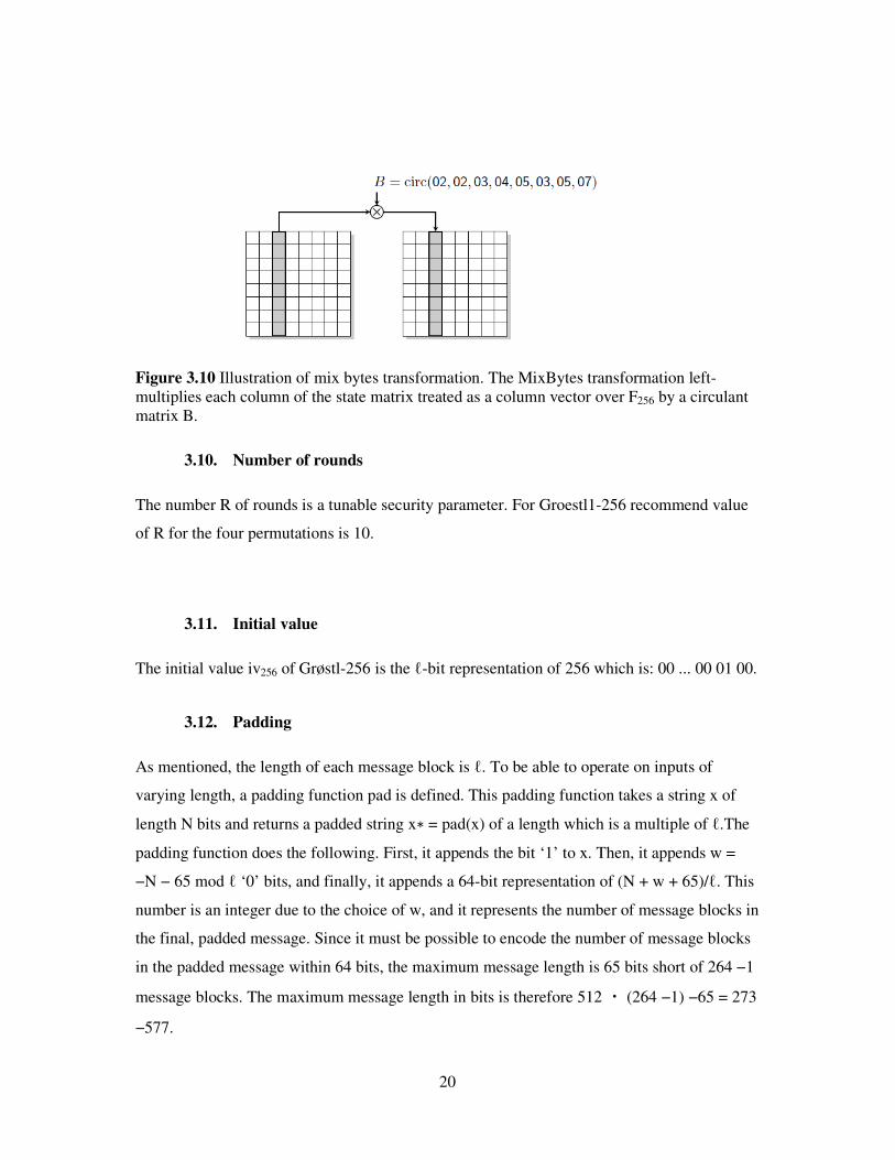
20
Figure 3.10 Illustration of mix bytes transformation. The MixBytes transformation left-multiplies each column of the state matrix treated as a column vector over F256 by a circulant matrix B.
3.10. Number of rounds
The number R of rounds is a tunable security parameter. For Groestl1-256 recommend value
of R for the four permutations is 10.
3.11. Initial value
The initial value iv256 of Grøstl-256 is the ℓ-bit representation of 256 which is: 00 ... 00 01 00.
3.12. Padding
As mentioned, the length of each message block is ℓ. To be able to operate on inputs of
varying length, a padding function pad is defined. This padding function takes a string x of
length N bits and returns a padded string x∗ = pad(x) of a length which is a multiple of ℓ.The
padding function does the following. First, it appends the bit ‘1’ to x. Then, it appends w =
−N − 65 mod ℓ ‘0’ bits, and finally, it appends a 64-bit representation of (N + w + 65)/ℓ. This
number is an integer due to the choice of w, and it represents the number of message blocks in
the final, padded message. Since it must be possible to encode the number of message blocks
in the padded message within 64 bits, the maximum message length is 65 bits short of 264 −1
message blocks. The maximum message length in bits is therefore 512 ・ (264 −1) −65 = 273
−577.
21
3.13. Summary
First, a message which is to be digested by Groestl is padded using the padding function
pad.The hash function then iterates a compression function f : 0, 1ℓ × 0, 1ℓ → 0, 1ℓ,
which is based on two permutations P and Q. Because of the output size n of the hash function
is 256 bits, ℓ = 512. At the end, the output of the last call to f is processed by the output
transformation, which reduces the output size from ℓ to n bits.

22
4. IMPLEMENTATION of SECURE HASH ALGORITHM-1 on FPGA
4.1. Architecture of The Overall System
A hash module cannot be used by itself because message integrity is sub part of a system.
These kinds of systems have a Central Processing Unit (CPU) and all data is received and
managed by CPU. If CPU needs a hash computation, routes message to hash module and
receives back the digest of the message. Because of that, a hash module must be designed
compatible to a CPU. Also, data communication between the hash module and CPU must be
fast to accomplish high speed calculation.
In the next implementation, hash module’s behavior is like as a RAM. This is because of all
CPU’s are compatible to operate a RAM. This makes hash module flexible to use on wide
range of systems. Additionally, software implementations of read and write data to a RAM is
easier. There are several block RAMs on Spartan 3E so that, a RAM on the system does not
consume device’s reconfigurable parts[5]. In Figure 4.1, overall system is imagined.

23
Figure 4.1 Overall system with CPU and FPGA. In the system, the CPU is a soft CPU that exists only in simulation.
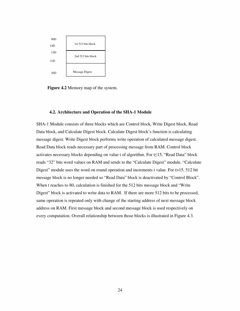
One port of Block RAM is connected to CPU and the other one is to SHA-1. Either of them
can read data any location on RAM but one of it is must write data to one location. Figure 4.2
illustrates memory map of Dual Port Block RAM. In SHA-1, message is computed as 512 bit
parts. There are two 512 bit blocks on RAM reserved for two message blocks and 160 bit
digest block to use as storage for computed digest. Two 512 bit block storage are used in
order to provide CPU and SHA-1 module use RAM simultaneously while SHA-1 using one
block, CPU can write next computation data to other block. By this method, performance is
boosted.
24
Figure 4.2 Memory map of the system.
4.2. Architecture and Operation of the SHA-1 Module
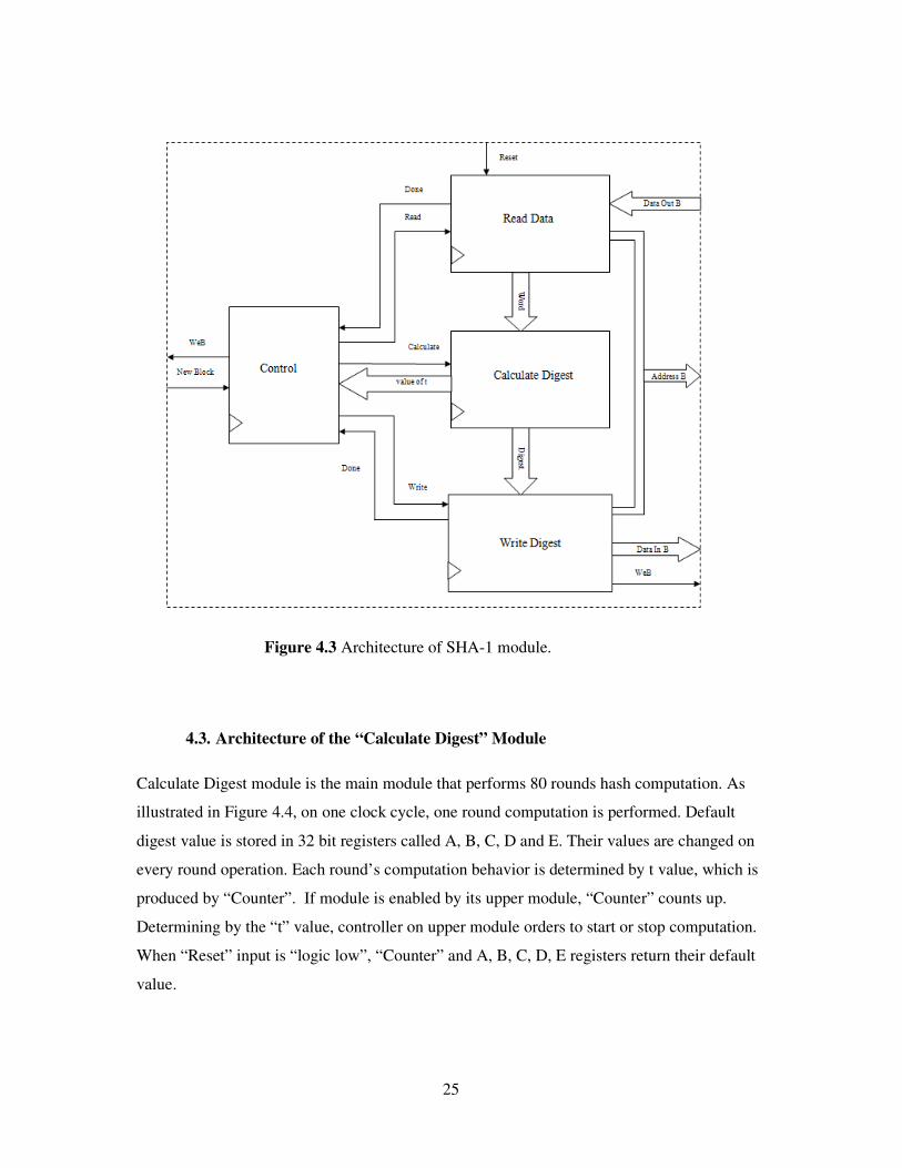
SHA-1 Module consists of three blocks which are Control block, Write Digest block, Read
Data block, and Calculate Digest block. Calculate Digest block’s function is calculating
message digest. Write Digest block performs write operation of calculated message digest.
Read Data block reads necessary part of processing message from RAM. Control block
activates necessary blocks depending on value t of algorithm. For t≤15, “Read Data” block
reads “32” bits word values on RAM and sends to the “Calculate Digest” module. “Calculate
Digest” module uses the word on round operation and increments t value. For t>15, 512 bit
message block is no longer needed so “Read Data” block is deactivated by “Control Block”.
When t reaches to 80, calculation is finished for the 512 bits message block and “Write
Digest” block is activated to write data to RAM. If there are more 512 bits to be processed,
same operation is repeated only with change of the starting address of next message block
address on RAM. First message block and second message block is used respectively on
every computation. Overall relationship between those blocks is illustrated in Figure 4.3.
00D
14D 1st 512 bits block
32D
15D 2nd 512 bits block
Message Digest
31D
36D
25
Figure 4.3 Architecture of SHA-1 module.
4.3. Architecture of the “Calculate Digest” Module
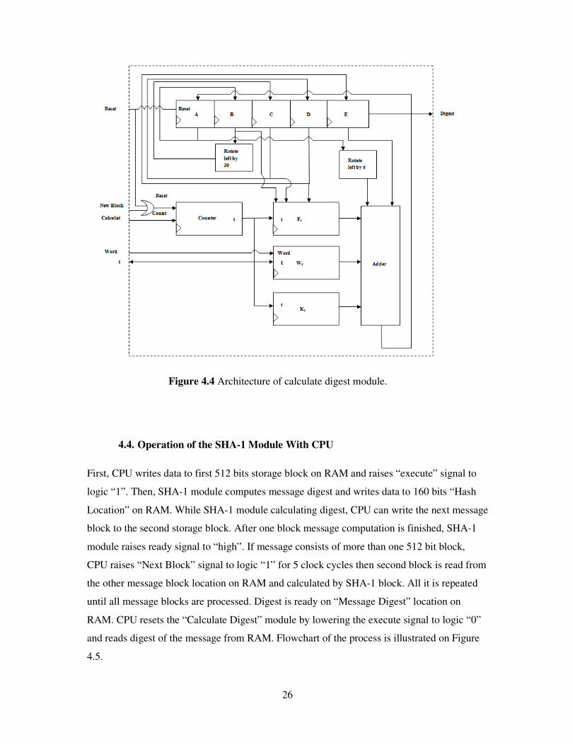
Calculate Digest module is the main module that performs 80 rounds hash computation. As
illustrated in Figure 4.4, on one clock cycle, one round computation is performed. Default
digest value is stored in 32 bit registers called A, B, C, D and E. Their values are changed on
every round operation. Each round’s computation behavior is determined by t value, which is
produced by “Counter”. If module is enabled by its upper module, “Counter” counts up.
Determining by the “t” value, controller on upper module orders to start or stop computation.
When “Reset” input is “logic low”, “Counter” and A, B, C, D, E registers return their default
value.
26
Figure 4.4 Architecture of calculate digest module.
4.4. Operation of the SHA-1 Module With CPU
First, CPU writes data to first 512 bits storage block on RAM and raises “execute” signal to
logic “1”. Then, SHA-1 module computes message digest and writes data to 160 bits “Hash
Location” on RAM. While SHA-1 module calculating digest, CPU can write the next message
block to the second storage block. After one block message computation is finished, SHA-1
module raises ready signal to “high”. If message consists of more than one 512 bit block,
CPU raises “Next Block” signal to logic “1” for 5 clock cycles then second block is read from
the other message block location on RAM and calculated by SHA-1 block. All it is repeated
until all message blocks are processed. Digest is ready on “Message Digest” location on
RAM. CPU resets the “Calculate Digest” module by lowering the execute signal to logic “0”
and reads digest of the message from RAM. Flowchart of the process is illustrated on Figure
4.5.

27
Figure 4.5 Operation process of SHA-1 module.
4.5. Simulation of the Implemented Design
Placing and routing of the design is done by Xilinx ISE9.2i. 1113 slices are occupied by the
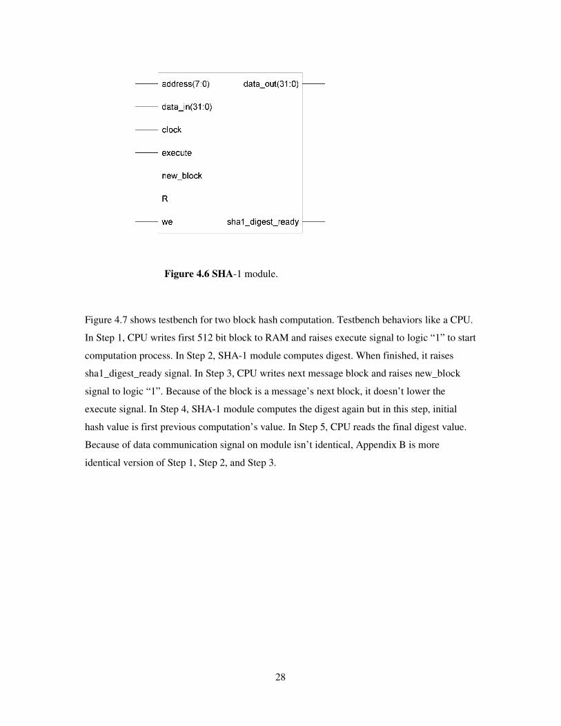
design. Figure 4.6 shows the implemented module block. The module can operate on
maximum 56 Mhz clock frequency.
28
Figure 4.6 SHA-1 module.
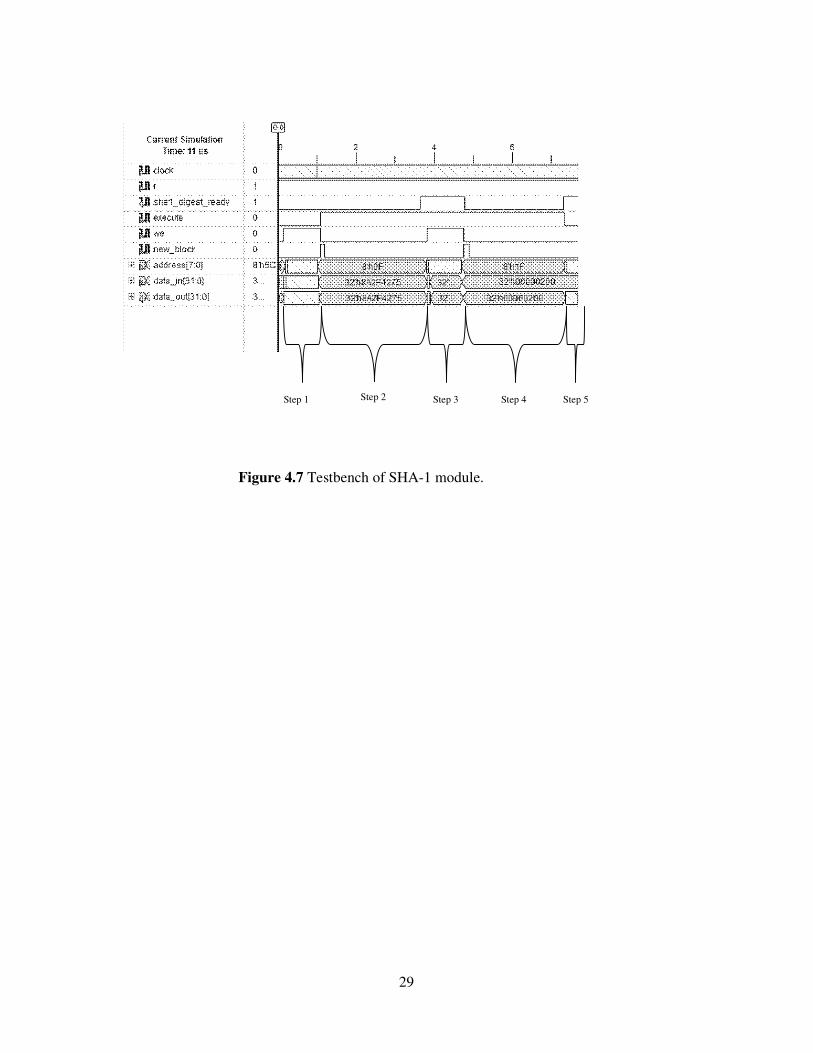
Figure 4.7 shows testbench for two block hash computation. Testbench behaviors like a CPU.
In Step 1, CPU writes first 512 bit block to RAM and raises execute signal to logic “1” to start
computation process. In Step 2, SHA-1 module computes digest. When finished, it raises
sha1_digest_ready signal. In Step 3, CPU writes next message block and raises new_block
signal to logic “1”. Because of the block is a message’s next block, it doesn’t lower the
execute signal. In Step 4, SHA-1 module computes the digest again but in this step, initial
hash value is first previous computation’s value. In Step 5, CPU reads the final digest value.
Because of data communication signal on module isn’t identical, Appendix B is more
identical version of Step 1, Step 2, and Step 3.
29
Figure 4.7 Testbench of SHA-1 module.
Step 1 Step 2 Step 3 Step 5 Step 4
30
5. IMPLEMENTATION of GROESTL-256 on FPGA
First step of the Groestl-256 is designing one round computation. All the design is almost the
repeated parts of one round computation. Main concept of reducing the area by using shift
registers. Shifting the registers doesn’t need additional device resources because of there are
shift registers on Spartan3E.
5.1. Implementation of Add Round Constant
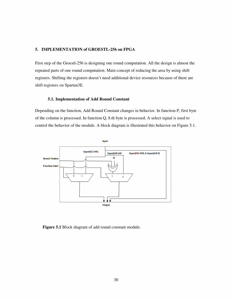
Depending on the function, Add Round Constant changes in behavior. In function P, first byte
of the column is processed. In function Q, 8.th byte is processed. A select signal is used to
control the behavior of the module. A block diagram is illustrated this behavior on Figure 5.1.
Figure 5.1 Block diagram of add round constant module.

31
5.2. Implementation of Sub Bytes
Because of Sub Bytes is operated on each byte with the same operation, one column’s Sub
Byte operation is done in 64 steps. It is illustrated on Figure 5.2.
Figure 5.2 Block diagram of sub bytes module.
5.3. Implementation of Shift Bytes
There is no logic implementation for shift bytes. Shift bytes process is done by only necessary
connection of signal to other module’s input.
5.4. Implementation of Mix Bytes
Mix bytes module is similar to sub bytes module. It consists of 8 column operation that every
column is multiplied by circular column vector which is
Counter
512 bits shift register
Comparator
Load
Comparator
0
64
S Box
Data[512:505] Shift
Done
Input
Output

32
circ[02 02 03 04 05 0305]. Instead of circulating the logic operation, vector variables are
shifted connected to input as illustrated on Figure 5.3.
Figure 5.3 Illustration of mix bytes module.
Counter
512 bits shift register
Comparator
Comparator
0
8
Data[512:449]
Done
Input
Output
Shift column
02020304050305 X
33
5.5. Construction of One Round
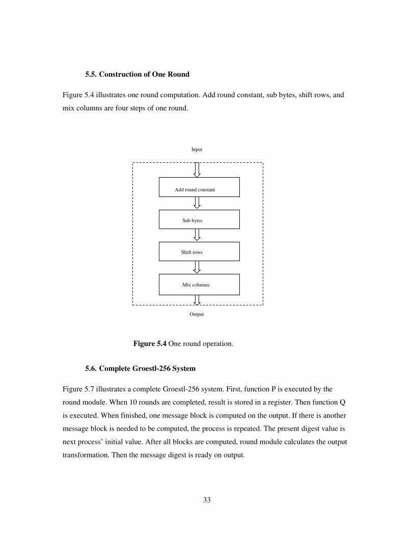
Figure 5.4 illustrates one round computation. Add round constant, sub bytes, shift rows, and
mix columns are four steps of one round.
Figure 5.4 One round operation.
5.6. Complete Groestl-256 System
Figure 5.7 illustrates a complete Groestl-256 system. First, function P is executed by the
round module. When 10 rounds are completed, result is stored in a register. Then function Q
is executed. When finished, one message block is computed on the output. If there is another
message block is needed to be computed, the process is repeated. The present digest value is
next process’ initial value. After all blocks are computed, round module calculates the output
transformation. Then the message digest is ready on output.
Add round constant
Sub bytes
Shift rows
Mix columns
Input
Output

34
Figure 5.7 Complete Groestl-256 system.
35
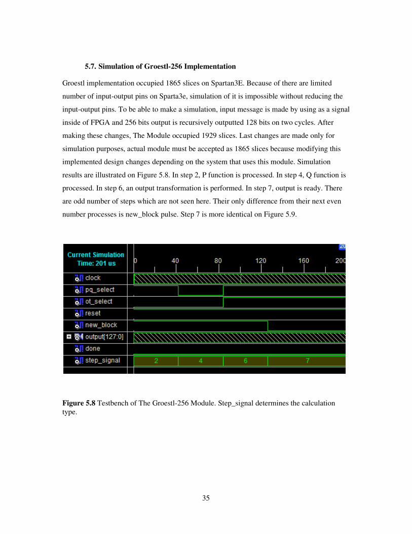
5.7. Simulation of Groestl-256 Implementation
Groestl implementation occupied 1865 slices on Spartan3E. Because of there are limited
number of input-output pins on Sparta3e, simulation of it is impossible without reducing the
input-output pins. To be able to make a simulation, input message is made by using as a signal
inside of FPGA and 256 bits output is recursively outputted 128 bits on two cycles. After
making these changes, The Module occupied 1929 slices. Last changes are made only for
simulation purposes, actual module must be accepted as 1865 slices because modifying this
implemented design changes depending on the system that uses this module. Simulation
results are illustrated on Figure 5.8. In step 2, P function is processed. In step 4, Q function is
processed. In step 6, an output transformation is performed. In step 7, output is ready. There
are odd number of steps which are not seen here. Their only difference from their next even
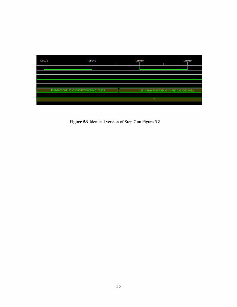
number processes is new_block pulse. Step 7 is more identical on Figure 5.9.
Figure 5.8 Testbench of The Groestl-256 Module. Step_signal determines the calculation type.
36
Figure 5.9 Identical version of Step 7 on Figure 5.8.

37
6. RESULTS and DISCUSSION
Most SHA-1 hash functions occupy approximately 700 slices between 1200 slices.
Implementation of SHA-1 is occupied 1113 slices that it can be seen large in comparison to
the other implementations. This is because there are several blocks to interface between RAM
and CPU. Interface modules occupy extra area. Still it is reasonable to use because of its
compatibility on RAM. 56 Mhz maximum clock frequency is reasonable too because of it is
faster than most processors.
Implementation of Groestl-256 is achieved its design goal as occupying 1865 slices on
Spartan3E. In comparison to 6582 slices implementation of Authors’ of Groestl[3] and 2486
slices of another implementation[6], its design goal of minimum area is achieved. 86 Mhz is
fast enough to use it on wide variety of systems.
To be able to detailed comparison on SHA-1 and Groestl-256, their output must be equal.
Because of there is no 160 bits version of Groestl, it couldn’t be implemented to compare both
two algorithms.

38
REFERENCES
[1] FIPS 180-1, 1995. Secure Hash Algorithm, US Department of Commerce, N.I.S.T, Washington.
[2] Kayser, R.F., 2007, Announcing Request for Candidate Algorithm Nominations for a New Cryptographic Hash Algorithm (SHA-3) Family. In: Federal Register. Volume 72. National Institute of Standards and Technology, Washington.
[3] J. Daemen and V. Rijmen.,1999, AES Proposal: Rijndael. AES Algorithm Submission, N.I.S.T., Washington.
[4] J. Daemen and V. Rijmen., 2002, The Design of Rijndael. Springer.
[5] Xilinx, 2009. Spartan-3 Generation FPGA User Guide,UG331
[6] Bernhard Jungk,2009, On Optimized FPGA Implementations of theSHA-3 Candidate Groestl, Fachhochschule Wiesbaden University of Applied Sciences.
39
APPENDIX A
S box values.

40
APPENDIX B
Testbench of SHA-1 module. Time range is 0 to 300 ns.
Testbench of SHA-1 module time range 300 to 600 ns.
41
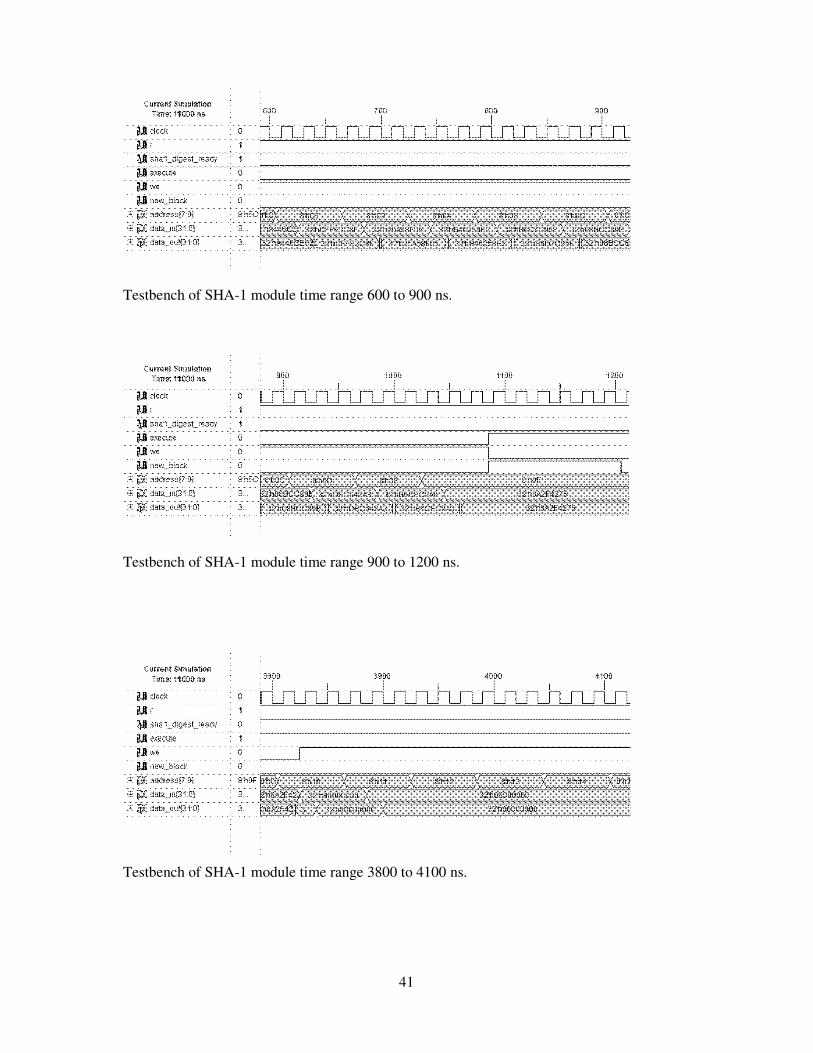
Testbench of SHA-1 module time range 600 to 900 ns.
Testbench of SHA-1 module time range 900 to 1200 ns.
Testbench of SHA-1 module time range 3800 to 4100 ns.
42
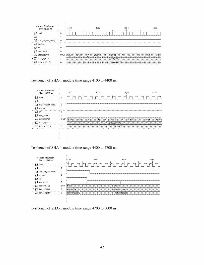
Testbench of SHA-1 module time range 4100 to 4400 ns.
Testbench of SHA-1 module time range 4400 to 4700 ns.
Testbench of SHA-1 module time range 4700 to 5000 ns.

43
Testbench of SHA-1 module time range 7300 to 7600 ns.
44
AUTOBIOGRAPHY
Oğuz Yelbey was born in Bursa/Mustafakemalpaşa in 1986. He completed elementary school
and middle school in there and completed Balıkesir Science High School in 2004. He was
accepted Istanbul Technical University Electronics Engineering Program in same year. He is
interesting in digital circuit design, cryptograpy and expecing to work on these subjects in
future.