investigations into design and control of power …
TRANSCRIPT

INVESTIGATIONS INTO DESIGN AND
CONTROL OF POWER ELECTRONIC
SYSTEMS FOR FUTURE
MICROPROCESSOR POWER SUPPLIES
Ravinder Pal Singh
NATIONAL UNIVERSITY OF SINGAPORE
2010

INVESTIGATIONS INTO DESIGN AND
CONTROL OF POWER ELECTRONIC
SYSTEMS FOR FUTURE
MICROPROCESSOR POWER SUPPLIES
Ravinder Pal Singh
(B.Tech(Hons), IIT Kharagpur, India)
A THESIS SUBMITTED
FOR THE DEGREE OF DOCTOR OF PHILOSOPHY
DEPARTMENT OF ELECTRICAL & COMPUTER ENGINEERING
NATIONAL UNIVERSITY OF SINGAPORE
2010

i
Acknowledgements
This thesis arose in part out of years of research that has been done since I
came to the Power Electronics group at National University of Singapore (NUS).
By that time, I have worked with a great number of people who deserve special
mention. They have contributed in assorted ways to the research and helped mak-
ing of this thesis possible. It is a pleasure to convey my gratitude to all of them in
my humble acknowledgment.
First and foremost, I offer my sincerest gratitude to my supervisor, Assoc.
Prof. Ashwin M. Khambadkone, who has supported me throughout my thesis
with his patience and knowledge, whilst allowing me the room to work in my own
way. His truly scientist intuition has made him a constant oasis of ideas, which
exceptionally inspired and enriched my growth as a student and as a researcher.
One simply could not wish for a better or friendlier supervisor. I am indebted to
him more than he knows.
I would also like to thank my co-supervisors Assoc. Prof. Ganesh S. Samudra
and Assoc. Prof. Yung C. Liang. They have been extremely enthusiastic and
supportive regarding this research. Without their encouragement and support this
study would have not been possible.
In my daily work I have been blessed with a friendly and cheerful group of
fellow students: (in alphabetical order) Amit K. Gupta, Anshuman Tripathi, Chen

Acknowledgements ii
Yu, K. Viswanathan, Kong Xin, Krishna Mainali, Sanjib Kr. Sahoo, Xu Xinyu
and Zhou Haihua. It was really wonderful working with them in the laboratory
and helping each other. I have learnt a lot through our miscellaneous chats. Thank
you all for being my friends.
Our lab officers Mr Woo, Mr Chandra, Mr Teo and Mr Seow have been a
great help. I appreciate their helpful nature and dedication in making laboratory
such a nice place to work.
There are some people outside the power electronics laboratory whose pres-
ence has made my stay at NUS really easy. I am also grateful to the members
of (my) Tennis Club. Our regular tennis sessions have helped me pull out from
stressed conditions. I have to also thank my apartment mates: Khattu, Debu, Sree
and Saurabh for their continued support and friendship.
My study at National University of Singapore was made possible through
the academic research grant for this project (R-263-000-305-112) and the graduate
research scholarship. I am extremely thankful to National University of Singapore
for the financial support.
And finally, no words suffice to express my heartfelt gratitude to those who are
closest to me. I would have never reached so far without the constant love and sup-
port of my parents and my sister. I would also like to thank my wife Navdeep whose
presence helped make the completion of my work possible. Thankyou Navdeep for
supporting me to work on the thesis during the weekends. Although it took me lit-
tle longer than expected, but now I have made it. Mom and Dad, this dissertation
is for you!

iii
Contents
Acknowledgements i
Summary viii
List of Tables xi
List of Figures xii
1 Introduction 1
2 Background and Problem Definition 8
2.1 Digital Control of Voltage Regulator Modules . . . . . . . . . . . . 8
2.1.1 Digital Control of DC-DC Converters . . . . . . . . . . . . . 10
2.1.2 Digital Control of high current VRMs . . . . . . . . . . . . . 12
2.2 Time Resolution of DPWM . . . . . . . . . . . . . . . . . . . . . . 15
2.3 Current Sensing Techniques . . . . . . . . . . . . . . . . . . . . . . 21

iv
2.3.1 Series resistance . . . . . . . . . . . . . . . . . . . . . . . . . 22
2.3.2 Inductor Voltage Sensing . . . . . . . . . . . . . . . . . . . . 24
2.3.3 MOSFET Rds,ON Sensing . . . . . . . . . . . . . . . . . . . 25
2.3.4 SenseFET . . . . . . . . . . . . . . . . . . . . . . . . . . . . 26
2.3.5 Current Transformers (CT) . . . . . . . . . . . . . . . . . . 27
2.3.6 Rogowski Coil . . . . . . . . . . . . . . . . . . . . . . . . . . 28
2.3.7 Hall Effect Sensor . . . . . . . . . . . . . . . . . . . . . . . . 28
2.4 Current Sharing in Paralleled Converters . . . . . . . . . . . . . . . 29
2.5 Improving the Transient Response of a Converter . . . . . . . . . . 35
2.6 Summary . . . . . . . . . . . . . . . . . . . . . . . . . . . . . . . . 40
3 Digital Control of VRMs 42
3.1 Introduction . . . . . . . . . . . . . . . . . . . . . . . . . . . . . . . 42
3.1.1 Controller Design Methods . . . . . . . . . . . . . . . . . . . 43
3.1.2 Frequency Domain Design . . . . . . . . . . . . . . . . . . . 44
3.1.3 Control Structure . . . . . . . . . . . . . . . . . . . . . . . . 47
3.1.4 Transformation to discrete-time controller . . . . . . . . . . 48
3.1.5 Current and Voltage Sensing . . . . . . . . . . . . . . . . . . 51
3.1.6 Controller Implementation . . . . . . . . . . . . . . . . . . . 53

v
3.1.7 Stability Analysis . . . . . . . . . . . . . . . . . . . . . . . . 57
3.1.8 Digital Dither . . . . . . . . . . . . . . . . . . . . . . . . . . 59
3.2 Experimental Results . . . . . . . . . . . . . . . . . . . . . . . . . . 61
3.3 Summary . . . . . . . . . . . . . . . . . . . . . . . . . . . . . . . . 64
4 Time Resolution of the DPWM 66
4.1 Introduction . . . . . . . . . . . . . . . . . . . . . . . . . . . . . . . 66
4.2 Proposed Scheme . . . . . . . . . . . . . . . . . . . . . . . . . . . . 67
4.2.1 Extending the scheme for finer resolution . . . . . . . . . . . 70
4.2.2 Effect due to variation in component values . . . . . . . . . 71
4.3 Simulation Results . . . . . . . . . . . . . . . . . . . . . . . . . . . 73
4.4 Experimental Results . . . . . . . . . . . . . . . . . . . . . . . . . . 75
4.5 Summary . . . . . . . . . . . . . . . . . . . . . . . . . . . . . . . . 79
5 Giant Magneto Resistive (GMR) effect based Current SensingTechnique 80
5.1 Introduction . . . . . . . . . . . . . . . . . . . . . . . . . . . . . . . 80
5.2 Proposed Method . . . . . . . . . . . . . . . . . . . . . . . . . . . . 81
5.2.1 Description . . . . . . . . . . . . . . . . . . . . . . . . . . . 81
5.2.2 Work on Magnetoresistive effect . . . . . . . . . . . . . . . . 84

vi
5.2.3 Magnetic Field distribution due to current carrying track . . 86
5.2.4 Performance Evaluation . . . . . . . . . . . . . . . . . . . . 90
5.3 Experimental Results . . . . . . . . . . . . . . . . . . . . . . . . . . 97
5.4 Summary . . . . . . . . . . . . . . . . . . . . . . . . . . . . . . . . 101
6 Current Sharing in Multiphase Converters 102
6.1 Introduction . . . . . . . . . . . . . . . . . . . . . . . . . . . . . . . 102
6.2 Proposed Scheme . . . . . . . . . . . . . . . . . . . . . . . . . . . . 104
6.2.1 Current Sensing . . . . . . . . . . . . . . . . . . . . . . . . . 104
6.2.2 Power Loss Analysis . . . . . . . . . . . . . . . . . . . . . . 107
6.2.3 Current Sharing . . . . . . . . . . . . . . . . . . . . . . . . . 108
6.2.4 Stability Analysis . . . . . . . . . . . . . . . . . . . . . . . . 112
6.2.5 Accuracy in current sharing . . . . . . . . . . . . . . . . . . 116
6.3 Experimental Results . . . . . . . . . . . . . . . . . . . . . . . . . . 118
6.4 Summary . . . . . . . . . . . . . . . . . . . . . . . . . . . . . . . . 120
7 Improving the Step-Down Transient Response 122
7.1 Introduction . . . . . . . . . . . . . . . . . . . . . . . . . . . . . . . 122
7.2 Proposed Scheme: Working Principle . . . . . . . . . . . . . . . . . 129
7.2.1 Switching Algorithm . . . . . . . . . . . . . . . . . . . . . . 132

vii
7.2.2 Output Capacitor Design . . . . . . . . . . . . . . . . . . . . 140
7.2.3 Slew rate determines the fall time . . . . . . . . . . . . . . . 140
7.2.4 Power Loss Analysis . . . . . . . . . . . . . . . . . . . . . . 142
7.2.5 Implementation of Proposed Scheme . . . . . . . . . . . . . 144
7.3 Experimental Results . . . . . . . . . . . . . . . . . . . . . . . . . . 144
7.4 Summary . . . . . . . . . . . . . . . . . . . . . . . . . . . . . . . . 147
8 Improving the Step-Up Transient Response 150
8.1 Introduction . . . . . . . . . . . . . . . . . . . . . . . . . . . . . . . 150
8.2 Proposed Scheme . . . . . . . . . . . . . . . . . . . . . . . . . . . . 152
8.2.1 Working Principle . . . . . . . . . . . . . . . . . . . . . . . . 156
8.2.2 Switched Capacitor Circuit Design . . . . . . . . . . . . . . 167
8.2.3 Slew rate determines the rise time . . . . . . . . . . . . . . . 169
8.2.4 Power Loss Analysis . . . . . . . . . . . . . . . . . . . . . . 170
8.2.5 Implementation of Proposed Scheme . . . . . . . . . . . . . 173
8.3 Experimental Results . . . . . . . . . . . . . . . . . . . . . . . . . . 173
8.4 Summary . . . . . . . . . . . . . . . . . . . . . . . . . . . . . . . . 179
9 Conclusions 180

viii
Appendix A 186
Bibliography 189
List of Publications 203

ix
Summary
Voltage Regulator Modules (VRMs) are used to provide power to the mi-
croprocessors. These modules are expected to deliver high currents upto 200A at
low output voltages of around 1.2V. In order to reduce losses, microprocessors use
dynamic voltage scaling, whereby the supply voltage to the microprocessor is ad-
justed with the computation load. To this end, the processor sends a 7-bit Voltage
Identification (VID) code to the VRM, that dictates its output voltage.
Since the digital interface to the microprocessor is available to the VRM, the
digital control is well suited for this purpose. However, the digital controllers have
the drawbacks of reduction in phase margin due to presence of Zero Order Hold
(ZOH) in Digital Pulse-Width Modulators (DPWM) and the limited resolution of
the DPWM output. The digital controllers designed in this work take into account
the reduction in phase margin due to presence of DPWM based ZOH. The effect
of quantization of filter coefficients is also analyzed and a minimum word length
filter structure is proposed for such controllers. In addition, a DPWM architecture
is proposed to improve the time resolution of the DPWM. The proposed scheme is
fabricated in the form of an Application Specific Integrated Circuit (ASIC) and is
verified using experimental results.
The VRM control requires the inductor currents to be sensed. Thus, a current
sensing method is described which is based on Giant Magneto Resistive (GMR)

x
effect. It is based on sensing the magnetic field generated by the flow of current.
Using fundamental equations of the field distribution, it is shown how the sensor can
be used for sensing the inductor current. Simulation and test results are provided
to assist the analysis.
Due to high currents, it becomes essential to have multiphase topology, where
the synchronous buck converters are connected in parallel such that each phase leg
carries only a fraction of the total output current. However, the current control
of such a topology will require N-current sensors. Thus, a sensing and sharing
algorithm is proposed which uses only one current sensor.
The control of a VRM ensures the voltage regulation during steady state
operation. However, the transient response of a DC-DC converter still gets gov-
erned by the fundamental equation of rate of change of inductor current. It is
proportional to the voltage across the inductor and inversely proportional to the
inductance. Two new circuit topologies are proposed which increases the slew rate
of inductor current during transient and thus improve the transient response of
the system. The performance of these topologies are verified with simulation and
experimental results. These schemes give another design freedom to optimally de-
sign the converters, resulting in lower inductor current ripple and requiring smaller
output capacitor as compared to the conventional schemes.
In all, this dissertation focuses on the design development and control of Volt-
age Regulator Modules for low voltage and high current applications. Theoretical
developments have been appropriately supported with analytical and experimental
results.

xi
List of Tables
3.1 Parameters of the interleaved buck converter prototype . . . . . . . 65
8.1 Slew rate comparison for different levels of input voltages in a buckconverter . . . . . . . . . . . . . . . . . . . . . . . . . . . . . . . . . 154

xii
List of Figures
1.1 Intel CPU transistors double every 18 months (source:[2]) . . . . . . 1
1.2 Historical power trend for Intel CPUs (source:[3]) . . . . . . . . . . 2
2.1 Block schematic of (a) Analog PWM controller and (b) Digital PWMcontroller. . . . . . . . . . . . . . . . . . . . . . . . . . . . . . . . . 10
2.2 Experimental results for observing the resolution of output voltage.Case (i): Single Edge, 100MHz clock; Case (ii) Dual Edge, 100MHzclock; Case (iii) Dual Edge, 200MHz clock. . . . . . . . . . . . . . . 20
2.3 Compensation network to remove the effect of parasitic inductance. 23
2.4 Inductor voltage sensing for obtaining the inductor current. . . . . . 25
2.5 Current sensing based on MOSFET Rds,ON . . . . . . . . . . . . . . 26
2.6 Current Sensing using SenseFET method. . . . . . . . . . . . . . . 27
2.7 Various current sharing schemes: (a) Current Mode control (b) Sin-gle wire current sharing scheme (c) Paralleled converters connectedwith Oring-connection (d) Current Sharing controller used in O-ringarchitecture (e) An automatic master scheme . . . . . . . . . . . . . 32
3.1 N-phase interleaved buck converter . . . . . . . . . . . . . . . . . . 44
3.2 Step response of the inductor current transfer functions with param-eter mismatch . . . . . . . . . . . . . . . . . . . . . . . . . . . . . 46
3.3 Cascaded control loop for 4-phase interleaved VRM . . . . . . . . . 48
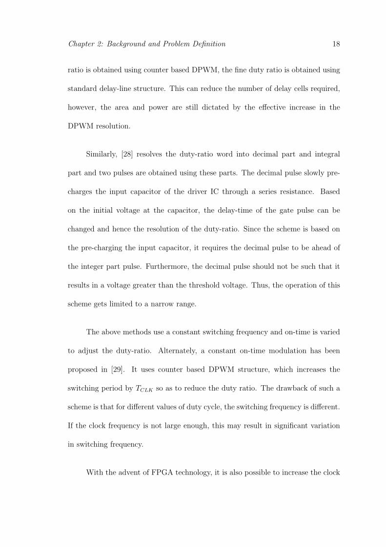
3.4 Bode plot of the system at various sampling rates . . . . . . . . . . 49

xiii
3.5 Effect of sampling frequency on phase margin of the compensatedsystems . . . . . . . . . . . . . . . . . . . . . . . . . . . . . . . . . 50
3.6 Bode plots of the system obtained by different methods. (i) In-ner Current Loop (ii) Voltage Loop with inner current loop closed.Curves: (a) Continuous time system, (b) Digital control system . . 51
3.7 (a) Filtering the voltage across the sense resistor to eliminate theeffects of parasitic inductance and (b) Output of the sense amplifierand the inductor current as measured using current probe. . . . . . 52
3.8 Schematic of digital controller design using FPGA . . . . . . . . . . 53
3.9 Effect of truncation on the filter coefficients in current controller . . 55
3.10 Direct Form : Filter realization . . . . . . . . . . . . . . . . . . . . 56
3.11 Photograph of the prototype of a 4-phase interleaved converter de-veloped in the lab . . . . . . . . . . . . . . . . . . . . . . . . . . . . 59
3.12 (a) Switching waveform patterns to realize 1-bit dither; (b) Switch-ing waveform patterns to realize 2-bit dither. . . . . . . . . . . . . . 60
3.13 Switching waveform patterns to realize 3-bit dither. . . . . . . . . . 61
3.14 Result showing the dynamic response of digitally controlled 4-phaseinterleaved converter for a step load variation from 15A to 70A . . . 62
3.15 Result showing the dynamic performance of the controller with adap-tive voltage positioning for a step load change from 15A to 80A . . 64
4.1 Schematic of the scheme for delaying the edges of the gate pulses . 68
4.2 Block schematic of the proposed scheme. The duty ratio is updatedbased on the least significant bits. . . . . . . . . . . . . . . . . . . . 69
4.3 Detailed schematic of the proposed scheme. The duty ratio is up-dated based on the least significant bits. . . . . . . . . . . . . . . . 72
4.4 Simulation results showing the performance of the proposed scheme.(a) Resulting voltage waveforms at capacitors C1, C2 and C3; (b)The PWM pulses obtained using the proposed scheme and (c) The4 possible duty ratios generated using the proposed scheme. . . . . 73

xiv
4.5 Simulation results showing the performance of three different controlmethods: (a) Analog control; (b)Conventional Digital Control and(c) Proposed Controller with duty ratio correction . . . . . . . . . . 74
4.6 Block schematic of the chip architecture . . . . . . . . . . . . . . . 75
4.7 Micrograph of the fabricated ASIC, named DigResv1 . . . . . . . . 75
4.8 Experimental results showing the variation of duty ratio in accor-dance with duty-ratio correction command (D1D2) . . . . . . . . . 76
4.9 Experimental prototype of the controller realized using the fabri-cated ASIC and the off-chip ADCs . . . . . . . . . . . . . . . . . . 77
4.10 Experimental results the output voltage regulation for proposed caseand conventional case. . . . . . . . . . . . . . . . . . . . . . . . . . 78
5.1 Working principle of Giant Magneto Resistive Effect. (a) Higher re-sistance due to anti-parallel magnetic moments, (b) Paralleled mag-netic moments reduces the electrical resistance and (c) Cross sec-tion along XX’ plane showing alignment of magnetic moments dueto magnetic field. . . . . . . . . . . . . . . . . . . . . . . . . . . . . 83
5.2 Wheatstone Bridge configuration available for sensing application. . 84
5.3 Magnetic field at point P due to a long current carrying PCB track. 87
5.4 (a) Magnetic Field Distribution as obtained from MATLAB (b)Magnetic Field Distribution as obtained from QuickField. . . . . . . 90
5.5 (a) Current detection using GMR magnetic field sensor whose axisof sensitivity is in the horizontal direction; (b) Input Output Char-acteristics of sensor at a supply voltage of 20V and (c) Linearity ofoutput voltage with varying supply voltage. . . . . . . . . . . . . . 92
5.6 Input-Output characteristics at two different temperatures (T =30oC and T = 70oC) . . . . . . . . . . . . . . . . . . . . . . . . . . 92
5.7 (a) Current flow through the bottom layer; (b) Current flow througha conductor placed on top on sensor; (c) Output voltage as obtainedfrom configurations A and B; (d) Placement of sensors on a widertrack; and (e) Input Output characteristics as obtained from config-uration C. . . . . . . . . . . . . . . . . . . . . . . . . . . . . . . . . 93

xv
5.8 Determining the location of physical sensor in the Sensor chip. . . . 94
5.9 Curves showing magnetic field distribution for varying track widthscarrying a current of 10A. . . . . . . . . . . . . . . . . . . . . . . . 96
5.10 Curves showing the location of points where magnetic field reducesto 90% in configuration A. Region 1© has magnetic field > 90% ofBmax and region 2© has magnetic field < 10% of Bmax. . . . . . . . 98
5.11 Experimental prototype of a buck converter which uses a GMR sen-sor for current sensing. A current probe is also used to observe theinductor current. . . . . . . . . . . . . . . . . . . . . . . . . . . . . 99
5.12 (a) Result showing the dynamic response of digitally controlled buckconverter for a step change in current reference; (b) Output voltagewith a step change in load current from 3A to 12A. . . . . . . . . . 100
5.13 Result showing the dynamic performance of the controller with adap-tive voltage positioning for a step load change. . . . . . . . . . . . . 101
6.1 Current Sensing in a 2-phase interleaved buck converter . . . . . . . 105
6.2 Current sensing in a 2-phase system using single sensor . . . . . . . 107
6.3 Two phase control architecture with duty ratio compensation forcurrent sharing . . . . . . . . . . . . . . . . . . . . . . . . . . . . . 109
6.4 The proposed control architecture as applied to a 4-phase interleavedconverter . . . . . . . . . . . . . . . . . . . . . . . . . . . . . . . . . 110
6.5 Simulation results showing the performance of the scheme duringstartup transient (a) Output voltage and output current, (b) Distri-bution of load current among individual phases, (c) Mismatch be-tween iL1, iL2 and iL3, iL4 and (d) Balanced inductor currents usingproposed scheme . . . . . . . . . . . . . . . . . . . . . . . . . . . . 111
6.6 (a) Simplified control architecture based on duty ratio compensa-tion for achieving current sharing (b) Constant duty ratio D beingupdated based on current mismatch . . . . . . . . . . . . . . . . . . 113
6.7 Simulation results showing the effect of increasing the gain of thecurrent sharing controller . . . . . . . . . . . . . . . . . . . . . . . . 115

xvi
6.8 Experimental results showing the output voltage and distribution ofinductor currents during load transients (a) Current controller is dis-abled (b) Result showing the dynamic performance of the controllerwhen current controller is enabled . . . . . . . . . . . . . . . . . . . 117
6.9 Experimental prototype of the two phase converter used to demon-strate the proposed current sensing scheme. . . . . . . . . . . . . . 118
6.10 Experimental results showing the dynamic performance of the con-troller with adaptive voltage positioning for a step load change . . . 120
7.1 Charging and discharging of the output capacitor during suddenchange in load current . . . . . . . . . . . . . . . . . . . . . . . . . 123
7.2 Region showing the comparison of voltage overshoot and undershootfor load transients of different magnitudes . . . . . . . . . . . . . . 126
7.3 (a) The proposed converter for improving the step-down load tran-sients. (b) Equivalent circuit during its three modes of operation. . 130
7.4 Difference in the slew rates - required and available . . . . . . . . . 132
7.5 Simulation result showing the performance of the proposed schemeduring a step change in current reference. (a) Conventional Scheme(b) Proposed scheme using the same converter parameters as theconventional scheme . . . . . . . . . . . . . . . . . . . . . . . . . . 134
7.6 Typical waveforms during step change in the load. The input voltageis switched after time t1 . . . . . . . . . . . . . . . . . . . . . . . . 136
7.7 Simulation result showing the performance of the proposed schemeduring a step change in load current. (a) Conventional Scheme (b)Proposed scheme using the same converter parameters as the con-ventional scheme . . . . . . . . . . . . . . . . . . . . . . . . . . . . 139
7.8 Reducing the fall time by increasing the slew rate of the inductorcurrent . . . . . . . . . . . . . . . . . . . . . . . . . . . . . . . . . . 141
7.9 (a) The proposed scheme using diodes. (b) The diodes are replacedby synchronous rectifiers . . . . . . . . . . . . . . . . . . . . . . . . 142
7.10 Schematic of digital controller design using FPGA . . . . . . . . . . 143

xvii
7.11 Experimental prototype of the buck converter used to demonstratethe proposed scheme. . . . . . . . . . . . . . . . . . . . . . . . . . . 145
7.12 Experimental result showing the performance of the system witha step change in reference current. (a),(b) Conventional converter(c),(d) Proposed buck converter . . . . . . . . . . . . . . . . . . . . 146
7.13 Experimental result showing the output voltage and inductor currentduring load transients in a buck converter with cascaded controlloops (a) Response of the Conventional buck converter (b) Responseof the proposed buck converter . . . . . . . . . . . . . . . . . . . . . 148
8.1 Working principle of the proposed scheme. The voltage across theinductor is changed by altering the input voltage . . . . . . . . . . . 152
8.2 Difference in the slew rates - required and available. The slew rateis increased by increasing the input voltage. . . . . . . . . . . . . . 157
8.3 Multi-level generator applied to a power converter . . . . . . . . . . 159
8.4 Simulation result showing the performance of the proposed schemeduring a step change in current reference. (a) Closed loop bandwidthof 50kHz (b) Closed loop bandwidth of 100kHz . . . . . . . . . . . 160
8.5 Discharging of output capacitor during sudden load change . . . . . 161
8.6 Typical waveforms during step change in the load. The input voltageis switched after time t1 . . . . . . . . . . . . . . . . . . . . . . . . 162
8.7 Simulation result showing the performance of the proposed schemeduring a step change in the load current. (i) Normal case whereinput voltage is kept constant, (ii) Converter having 2 levels of inputvoltage and (iii) Converter having 5 levels of input voltage. . . . . . 166
8.8 Charge supplied by the switched capacitor network to increase theslew rate of inductor current. . . . . . . . . . . . . . . . . . . . . . 167
8.9 Reducing the rise time by increasing the slew rate of the inductorcurrent . . . . . . . . . . . . . . . . . . . . . . . . . . . . . . . . . . 170
8.10 Block schematic of the proposed scheme showing a buck converterand a switched capacitor network at its input . . . . . . . . . . . . 171
8.11 Block schematic of the proposed scheme . . . . . . . . . . . . . . . 174

xviii
8.12 Experimental prototype of the buck converter used to demonstratethe proposed scheme. . . . . . . . . . . . . . . . . . . . . . . . . . . 175
8.13 Experimental result showing the performance of the system with astep change in reference current. (a) Conventional converter withinput voltage constant (b) Converter with switched input voltage . 176
8.14 Experimental result showing the output voltage and inductor currentduring load transients in a buck converter with cascaded V+I controlloops (a) Conventional converter with input voltage constant (b)Converter with switched input voltage . . . . . . . . . . . . . . . . 177
8.15 Experimental result showing the output voltage and inductor currentduring load transients in a buck converter with cascaded V+I controlloops (a) Conventional converter with input voltage constant (b)Converter with switched input voltage . . . . . . . . . . . . . . . . 178
A.1 Charging and discharging of the output capacitor during suddenchange in load current . . . . . . . . . . . . . . . . . . . . . . . . . 186

xx
List of Symbols
Vin Input voltage (V)
Vout Output voltage (V)
Vref Reference voltage (V)
Io Output current (A)
∆Io Change in output current (A)
IL Inductor current (A)
∆IL Inductor current ripple (A)
vref Reference voltage for AVP (V)
io Instantaneous output current (A)
Rdroop Droop resistance for AVP (Ω)
L Circuit inductance (H)
Lk Inductance of phase k (H)
rL dc resistance of inductor (Ω)
Co Output capacitance (F)
rc Equivalent resistance of output capacitor (Ω)
Cin Input Capacitance (F)
rcin Equivalent resistance of input capacitor (Ω)

xxi
fs Switching frequency (Hz)
Ts Switching period (s)
fCLK Clock Frequency (Hz)
TCLK Time period of the clock (Hz)
NADC ADC Resolution (bits)
NDPWM DPWM Resolution (bits)
ρu Slew rate of inductor current during step-up transient (A/s)
ρd Slew rate of inductor current during step-down transient (A/s)
ρ1 Available slew rate of inductor current (A/s)
ρ2 Revised slew rate of inductor current (A/s)

1
Chapter 1
Introduction
Microprocessor scaling has consistently adhered to Moores law [1], thereby
doubling the transistors every 18 months, as seen in Fig. 1.1 [2]. Increasing transis-
tor density combined with the performance demanded from next-generation micro-
processors result in increased processor power. Scaling of transistors also necessi-
tates a reduction in the operating voltages both for reliability of the finer-dimension
devices and for reducing the power consumed by the microprocessor.
1970 1975 1980 1985 1990 1995 2000 2005 2010Year
103
Transistors
104
105
106
107
108
109
1010
Moore’s Law Continues
4004
8008
8080
8086
Intel 286 Intel 486
Intel Pentium
Intel Pentium II
Intel Pentium III
Intel Pentium 4
Intel Itanium
Intel Itanium 2
Itanium 2 (9MB Cache)
Intel 386
8-Core Xeon
Quad-Core Itanium
Dual-Core Itanium 2
Figure 1.1: Intel CPU transistors double every 18 months (source:[2])

Chapter 1: Introduction 2
The power loss is PL ∝ N · C · (Vdd)2 · fclk where, N is the number of cells,
Vdd is the supply voltage, fclk is the clock frequency and C is the capacitive loading
of a single CMOS cell. Since the number of CMOS cells per die area is growing
as predicted by the Moore’s law, the net result is increased power consumption
of the future microprocessors. Historical data on the increase in power for Intel
microprocessors is included in Fig. 1.2 [3][4]. It is seen that the power doubles
approximately every 36 months. This is attributed to simple analytical relation
based on increasing clock frequency, transistor count and less aggressive voltage
reduction. However, since the power consumption of the chip is large, any reduction
in voltage will increase the supply current drawn by the microprocessors.
Figure 1.2: Historical power trend for Intel CPUs (source:[3])
According to Intel′s prediction, one can expect the power consumption of
around 200W. The supply voltage will drop to below 1V and the supply current
will be around 200A [4]. The output voltage tolerance is required to be less than
1% even in the presence of high slew rates of current drawn by the microprocessors.
These tight required regulations, place an enormous burden on the circuits that
provides power to the chip. These circuits are collectively referred to as Voltage
Regulator Modules (VRMs).

Chapter 1: Introduction 3
Normally the VRMs supplying power to the microprocessors derive power
from a 12V regulated bus [5][6]. For low voltage low current VRMs, a synchronous
buck converter has been found to be suitable for such conversion. However if a single
stage buck converter is used in 12V to 1V, 200A VRM, then due to the stringent
voltage regulation requirements and due to the large slew rates of the current, large
output filter will be required. Due to limited space on motherboards, such size of
VRMs would not be feasible [7].
To meet the requirements of limited space on motherboard and the tight reg-
ulations, the power conversion must be done at higher switching frequencies. This
will reduce the size of the required components and it will provide a fast transient
response. The amount of required output filter size can also be reduced using an
interleaving multiphase topology. With multiphase topology, the synchronous buck
converters are connected in parallel, such that each phase leg carries only a fraction
of the total output current. By operating the various converters in a phase-shifted
manner, such a topology can offer decreased magnitude of output voltage ripple. It
also helps in increasing the frequency of the voltage ripple. Thus, the size of filter
components can be reduced to a greater extent.
In an interleaved buck converter topology, it is important to share the currents
equally among various phases. However, due to variation in the inductor values,
differences of components, connections and layout results in unequal current dis-
tribution among phases. This causes uneven distribution of losses and reduces
the overall efficiency. Thus, appropriate current sharing mechanism is required to

Chapter 1: Introduction 4
distribute the current evenly among the phases.
In order to maintain good current sharing among the phases a current sensor
needs to be added in a DC-DC converter. For a paralleled converter system, sensor
needs to be added for each converter. The performance of any such design will
depend on the performance of the current sensing technique. The output of current
sensor should be linear in the operating range of VRMs and should have high
bandwidth so as to sense the currents during load transients with high slew rate.
Apart from the high output currents, the VRMs are expected to maintain tight
voltage regulation even in the presence of such large load current transients.
This thesis focuses on the design development and control of Voltage Regu-
lator Modules for low voltage and high current applications. All the above issues
related to the VRM design have been considered. Followings are the major contri-
butions of this work.
• The first important contribution is the development of digital controllers for
interleaved buck converters. Problem of variations in inductor values among
different phases has been brought out and a method to overcome them has
been discussed. Such digital controllers can be implemented with simple Field
Programmable Gate Array (FPGA) development kits for quick prototyping.
• Such implementation uses a Digital Pulse Width Modulator (DPWM) to con-
trol the duty ratio of the gate pulses. However, the time resolution of these
pulses gets limited by the operating clock frequency of the FPGA board.

Chapter 1: Introduction 5
Thus, a scheme is presented which improves the time resolution as com-
pared to the conventional architecture. The proposed scheme is fabricated
in 0.35µm Austria Micro-Systems (AMS) process and is verified with exper-
imental results.
• The third contribution is an isolated current sensor which works on the mag-
netic field developed by the current to be measured. Comprehensive analysis
to evaluate the feasibility of such a current sensor has been carried out. Ex-
perimental results are presented to verify the working principle of such a
sensor, when applied to high current applications.
• In an interleaved buck converter, a current sensor is normally employed for
each phase so as to achieve current sharing among individual phases. De-
tailed analytical study has been done to establish the feasibility of a scheme
which can reduce the number of sensors in such a system. Thus, a scheme
is presented which uses a single current sensor to sense various currents and
is independent of number of phases. The performance of such a scheme is
verified with experimental results.
• In a buck converter, the slew rate of inductor current gets limited by the cir-
cuit parameters. The slew rate can be increased either by increasing the volt-
age across the inductor or by reducing the inductance. However, reduction
of inductance will result in higher losses and on the other hand, the voltage
across the inductor is limited by the input and output voltage. Another sig-
nificant contribution is the development of circuit topology which increases

Chapter 1: Introduction 6
the slew rate of inductor current during dynamics. The performance of such
a topology is verified with simulation and experimental results.
• Analytical verifications are presented to show that the step down load tran-
sient is more critical in a buck converter with low conversion ratio. Hence, a
new topology is developed which improves the step-down load transients in
such low voltage buck converters.
Altogether, this dissertation attempts to solve the above mentioned issues.
There are 9 chapters in this dissertation, each with a specific focus. The organiza-
tion of the thesis is as follows.
• The next chapter will give a literature survey of various solutions aimed to
address the above mentioned issues. The performance of these methods has
been critically analyzed. This will help to bring out the focus of the present
work and also recognize the problems.
• Starting from the basic concepts, the need for a fast digital controller is
discussed in chapter three. It gives the design development of such a controller
which can be easily implemented on an FPGA platform.
• The fourth chapter discusses the limited time resolution of the gate pulses. It
presents a hybrid digital PWM architecture which helps to improve the time
resolution of such pulses.
• The fifth chapter evaluates various sensors which are used for current sensing.
Identifying the need for a current sensor which is suitable for given low voltage

Chapter 1: Introduction 7
and high current applications, a current sensing method is proposed.
• In an N-paralleled converter N current sensors are required. The sixth chapter
discusses the current sharing scheme which uses single sensor to sense the
inductor current in a multiphase converter.
• Two new circuit topologies which improves the step-up and step-down load
transients have been covered in chapter seven and chapter eight respectively.
• Finally, chapter nine concludes this thesis highlighting the major contribu-
tions of this research.

8
Chapter 2
Background and ProblemDefinition
2.1 Digital Control of Voltage Regulator Mod-
ules
Advances in processor technology have posed stringent requirements on the
voltage regulator module (VRM) design. Due to stringent regulation requirements,
the design of next generation VRMs need a thorough understanding of the perfor-
mance and design trade-offs. The supply voltage of the microprocessor will drop
to below 1V and the supply current will be around 200A [4]. For microprocessor
loads, high slew rates of VRM output current are expected. In addition, the VRM
output voltage regulation is required to be less than ± 1%.
In order to reduce losses, microprocessors use dynamic voltage scaling, whereby
the supply voltage of the microprocessor is adjusted with the computational load
[8]. To this end, the processor sends a 7-bit Voltage Identification (VID) code to

Chapter 2: Background and Problem Definition 9
the VRM, that dictates its output voltage. Depending on the VID code, the output
voltage level changes by 6.25mV step every 5µs [6].
Usually the analog control methods have been proposed for VRMs [7], [9],
[10], [11]. Fig. 2.1(a) shows a typical analog voltage-mode control method. In this
implementation, the digital VID code has to be converted to its equivalent analog
signal Vref . An error amplifier processes the output voltage error (Vref − Vout) and
realizes a compensator for the desired control action. It requires proper selection of
passive components for realizing the desired compensators. However, component
variations and aging effect are also commonly seen in analog control design which
affects the system performance. Moreover, the presence of noise in the system
makes it difficult to achieve a resolution of 6.25mV.
Since the reference voltage is available to the VRM as a digital code, it can
be easily incorporated into the digital controllers. Recently, the digital controllers
have gained attention due to their low quiescent power, immunity to analog com-
ponent variations, ease of implementing advanced controller architecture and other
advantages. Moreover, developments in Field Programmable Gate Arrays (FPGA)
makes it a useful platform to design and validate the digital controllers. The con-
trollers may then be fabricated to result in a digital controller integrated circuit
(IC). However, the disadvantages of digital control include finite word length effects
and sampling time delay due to presence of Zero order Hold (ZOH).
Although digital control is suited for VRM due to the digital interface to the

Chapter 2: Background and Problem Definition 10
Power Stage
Vout
Sense
Amplifier
A/D
Digital
CompensatorDPWM
Gate Drivers
Dead Time
To MOSFETs
Vout
Vin
Vref(k)
Load
Vout(k)D(k)
1/fCLK
Power Stage
Vout
Gate Drivers
Dead Time
To MOSFETs
Vin
Vref
Load
- +
-
+
Error
Amplifier
PWM
Comparator
Z1
ZFBd(t)
Oscillator
Q
Q
R
S
(a)
(b)
fCLK(fs)
(fs)
Figure 2.1: Block schematic of (a) Analog PWM controller and (b) Digital PWMcontroller.
microprocessor and the other generic advantages of digital control, it is a challenge
to deliver the performance required of the next generation VRMs [4].
2.1.1 Digital Control of DC-DC Converters
A comparison of various digital control design approaches for DC-DC con-
verters have been presented in [12] and [13].

Chapter 2: Background and Problem Definition 11
A digital proportional + integral + derivative (PID) controller for DC-DC
applications presented in [14], uses a lookup table. The lookup table maps the
controller behavior to various values of the digitized error signal. Since the size of
the lookup table depends on the range of the error signal and the desired regulation
of the output voltage, this is scheme only suitable for small range of operating
conditions.
For hand-held devices, DC-DC converter power supplies have to operate very
efficiently to prolong battery life. To this end, [15] uses a load dependent operation
that alternates between two discrete switching frequencies for the same output
voltage. It achieves high efficiency by operating the converters in discontinuous
conduction mode at light loads.
As opposed to analog control methods, digital control adds quantization noise.
High resolution is required to minimize quantization noise. To this end, a high
resolution Analog to Digital Converter (ADC) is required. Moreover, a high speed
of conversion is necessary to achieve high control bandwidth. Such ADCs need
large floor space in digital ICs. To overcome the problem of large floor space, [16]
proposes a delay line ADC. However, due to process and temperature variations,
the delay cannot be defined precisely. Hence, it requires calibration of ADC.
Increasing the resolution of ADC creates another problem. It has been shown
[17] that, if the resolution of ADC is greater than the resolution of the Digital
Pulse-Width-Modulator (DPWM) counter and there is no integral control action,

Chapter 2: Background and Problem Definition 12
a limit cycle oscillation occurs. Therefore, it has been recommended that the res-
olution of DPWM be at least 1 bit higher than that of ADC. However, for a given
clock frequency, increasing the DPWM resolution results in a lower switching fre-
quency. To meet, the high switching frequency demand along with high resolution
of DPWM, few methods have been proposed. For example, a digital PWM using
a ring-oscillator-multiplexer scheme is implemented in [18]. On the other hand, a
dither signal is used to increase the effective DPWM resolution while using a low
resolution of the PWM counter [17] .
2.1.2 Digital Control of high current VRMs
Most digital control schemes for VRMs, proposed so far, are voltage-mode
control. However, there are few examples of current mode control such as [19] and
[20]. Current control facilitates current sharing in interleaved converters, which is
a popular topology for VRMs.
A low complexity digital peak current control is presented in [20]. However, it
results in variable switching frequency operation. The scheme uses low resolution
digital-to-analog converters (DACs) to generate a droop compensated current and
voltage reference signal. These are compared with the actual signals with help of
an analog comparators. Though the scheme achieves a high current operation with
a fast current control, its resolution is dictated by the DACs.
On the other hand an average current mode or voltage mode control, uses

Chapter 2: Background and Problem Definition 13
the average value of the sampled state variable, respectively.
In order to achieve high bandwidth, over-sampling is used. In over-sampling,
sufficient number of samples of the state variable are taken within a switching
period. The average value of the state variable is then computed over the switching
period. This average value is used to compute the duty ratio for the next switching
period [21]. This introduces a ZOH behvaior in the system.
On the other hand, multi-sampling can be used to reduce the effect of ZOH
in DPWM. In multi-sampling, multiple samples are taken within the switching
period. Hence, the value of the state variable that is compared with the DPWM
ramp is not equal to the sampled and held value at the start of the switching period.
However, this method can introduce high frequency ripple due to the aliasing error
in the sampled variable. To overcome this error, a repetitive filter is proposed [22]
that eliminates the aliasing effect and thus achieves a control bandwidth that is
similar to that of analog control.
A predictive current control [19] is proposed for VRMs. The scheme re-
quires the converter parameter like inductor value (L) to formulate the control law.
However, such scheme will require a disturbance observer to compensate for the
unmodeled dynamics. An appropriate gain has to be calculated for the distur-
bance observer. Insufficient gain reduces the response time of the system while
high gain causes limit cycle. Moreover, for current sharing, precise value of each
phase inductor is required.

Chapter 2: Background and Problem Definition 14
Previously reported models of interleaved converters assume all the inductors
to be the same, in which case, the problem is reduced to having N synchronous
buck converters in parallel. In practice, it is very difficult to have same value for
all inductors. There can be ±5− 10% variation in the inductor values, resulting in
asymmetry in the phases. This results in uneven distribution of inductor current
among individual phases. Thus, appropriate current sharing mechanism is required
to distribute the current evenly among the phases. A current mode control is used
to solve this problem which takes into account the variations among inductance
values.
Thus, a digital control scheme with individual phase current loops is used to
achieve current sharing during dynamics and steady state operation. In a typical
digital control system, the duty ratio command is the fed to the Digital Pulse-
Width-Modulator (DPWM) to produce the gate signals for the converter. Due to
the nature of DPWM, such digital control systems are characterized by the presence
of the Zero-Order-Hold (ZOH). Therefore the performance of these systems is a
function of DPWM switching period. Thus, appropriate digital controllers need to
be designed taking into account the performance degradation due to presence of
DPWM based ZOH. Moreover, the performance also depends on quantization error,
round-off and truncation errors. The effect of quantization of filter coefficients need
to be analyzed and a minimum word length filter structure should be obtained.

Chapter 2: Background and Problem Definition 15
2.2 Time Resolution of DPWM
Most digital control schemes use DPWM to obtain the gate pulses. However,
the performance of such systems get limited due to the finite resolution of the
DPWM pulses.
A typical block schematic for implementing a digital control is shown in Fig.
2.1(b). The control algorithm takes the digitized error signal (Vref (k) − Vout(k))
and computes the discrete set of duty-cycle command D(k). The duty ratio word
is processed by DPWM which generates the gate pulses at the desired switching
frequency (fs).
To implement this, a counter based DPWM is commonly used which provides
high linearity and is simple to design. However, the minimum time resolution of
such a DPWM is equal to the time period of its clock. This puts stringent require-
ment on clock frequency if fine resolution of duty ratio is required, for example, in
a VRM type application.
It has been shown in [10] and [23] that it is advantageous to obtain the VRM
output from a 5V bus. Thus, for our analysis the input voltage has been chosen as
Vin = 5V . For obtaining ∆Vout = 6.25mV with Vin = 5V , we need a resolution of
∆D =∆Vout
Vin
= 0.00125 (2.1)
If the switching frequency is fs = 1MHz, this corresponds to a time resolution of
∆t = 1.25ns. For obtaining such time resolution, the counter based DPWM has

Chapter 2: Background and Problem Definition 16
to be operated at 800MHz!
In general, for achieving N-bit resolution of the DPWM block, it needs to be
clocked at 2N .fs, where fs is the switching frequency of the converter. For example,
an 8-bit DPWM generating switching frequency of fs = 1MHz will require a clock
frequency of fCLK = 256MHz and so on. To meet, the high switching frequency
demand along with high resolution of DPWM, various methods have been proposed
in the past. Some of these methods are described below.
It has been established that if the resolution of the DPWM counter is smaller
than the resolution of ADC and there is no integral control action, a limit cycle
oscillation occurs [17]. Therefore, it has been recommended that the resolution of
DPWM be at least 1-bit higher than that of ADC. Thus, a dither signal is used
to increase the effective DPWM resolution while using a lower-resolution DPWM
counter. Introducing dither increases the overall resolution of the DPWM but it
results in sub-harmonic oscillations. For M-bit increase in effective DPWM resolu-
tion, it will result in sub-harmonic oscillation at fs/2M , where fs is the switching
frequency of the converter. Moreover, a limit on the maximum possible increase in
effective resolution is established in [17].
In order to increase the resolution of DPWM, a ring-oscillator-multiplexer
based DPWM scheme is proposed [18]. The time-resolution of the output depends
on the delay introduced by the cells in the ring-oscillator. However, for N-bit
resolution this will require 2N stage oscillator and a 2N -to-1 multiplexer to select the

Chapter 2: Background and Problem Definition 17
appropriate signal from the ring oscillator. Such an implementation of the DPWM
module requires large silicon area, which increases exponentially with the number
of resolution bits (N). Moreover, high-frequency operation of such an oscillator
results in power loss. In order to reduce power, tapped delay line structure has
been proposed [24], [25]. The tapped delay line operates at the switching frequency,
thus reducing the power significantly. However, this scheme also requires 2N stage
delay line and a 2N -to-1 multiplexer to select the appropriate signal from the delay
line, which results in large silicon area.
In order to reduce the silicon area, segmented delay line has been proposed
[25]. In such a scheme, the delay line is segmented into groups of smaller delay
lines. The desired signal can be selected by using smaller multiplexer. In order
to increase the resolution, such segments need to be cascaded and an appropriate
multiplexer is used. Another variation of segmented delay line scheme is segmented
binary weighted delay line based DPWM [26]. In such a scheme, the delay cells are
designed to provide binary weighted delays. Although the number of delay cells is
reduced, but the size of individual delay cells will vary as to provide the desired
delay. The larger delay is generated by simply replicating the basic delay cells,
resulting in the same overall number of delay cells.
Silicon area resulting from delay cells can be reduced by using a hybrid ap-
proach [16], [27]. It resolves the high-resolution duty ratio word into two groups:
coarse duty-ratio command comprising of the most-significant bits and fine duty-
ratio command comprising of the lower-significant bits. While the coarse duty
Chapter 2: Background and Problem Definition 18
ratio is obtained using counter based DPWM, the fine duty ratio is obtained using
standard delay-line structure. This can reduce the number of delay cells required,
however, the area and power are still dictated by the effective increase in the
DPWM resolution.
Similarly, [28] resolves the duty-ratio word into decimal part and integral
part and two pulses are obtained using these parts. The decimal pulse slowly pre-
charges the input capacitor of the driver IC through a series resistance. Based
on the initial voltage at the capacitor, the delay-time of the gate pulse can be
changed and hence the resolution of the duty-ratio. Since the scheme is based on
the pre-charging the input capacitor, it requires the decimal pulse to be ahead of
the integer part pulse. Furthermore, the decimal pulse should not be such that it
results in a voltage greater than the threshold voltage. Thus, the operation of this
scheme gets limited to a narrow range.
The above methods use a constant switching frequency and on-time is varied
to adjust the duty-ratio. Alternately, a constant on-time modulation has been
proposed in [29]. It uses counter based DPWM structure, which increases the
switching period by TCLK so as to reduce the duty ratio. The drawback of such a
scheme is that for different values of duty cycle, the switching frequency is different.
If the clock frequency is not large enough, this may result in significant variation
in switching frequency.
With the advent of FPGA technology, it is also possible to increase the clock

Chapter 2: Background and Problem Definition 19
frequency. Delay-locked loops (DLL) are commonly present on FPGA for obtaining
the phase shifted clocks. Using these DLLs, it is possible to multiply or divide the
clock frequency. The multiple of clock frequency is used to obtain the finer duty
ratio pulses [30]. However, an increase in clock frequency by 4 will only result in
a 2-bit increase in effective resolution of DPWM. Since the modern FPGAs can
provide a maximum of 4fCLK , the scheme results in a limited improvement.
In order to overcome the limitations of the DLL method, Digital Clock Man-
ager (DCM) circuit has been employed [31]. DCM is present on modern high-end
FPGA boards and is essentially a delay locked loop along with the digital frequency
synthesizer and a phase shifter [32], [33]. It can provide phase shifted versions of
the input clock - 0 deg, 90 deg, 180 deg and 270 deg along with the multiples of
input frequency 2fCLK and 4fCLK . Using one DCM, a 2-bit increase in effective
resolution of DPWM can be achieved. Such DCM circuits need to be cascaded
for increasing the resolution further. In cascaded DCM structure, the subsequent
DCM stage is operated at twice the clock frequency of its preceding DCM stage.
In comparison, both the DLL scheme [30] and DCM architechture [31] benefit from
the FPGA on board resources to implement the delay line. The latter relies on the
phase of the input clock while the former relies on the multiple of the system clock.
In addition to increasing the system clock frequency, both the edges of the
clock can also be exploited. In order to implement this, a counter based DPWM is
used and the converter is operated in open-loop. Clock frequency of 100MHz and
200MHz is used and both the edges are used to increment the counter. As seen

Chapter 2: Background and Problem Definition 20
Figure 2.2: Experimental results for observing the resolution of output voltage.Case (i): Single Edge, 100MHz clock; Case (ii) Dual Edge, 100MHz clock; Case(iii) Dual Edge, 200MHz clock.
from Fig. 2.2, increasing the clock frequency can improve the duty ratio resolution
and hence the output voltage variation. Using (2.1) we have
∆Vout = ∆D · Vin (2.2)
For 100MHz clock, we have ∆D = 0.01 or ∆D = 0.005 for single edge and
dual edge scheme respectively. Thus, for an input voltage of Vin = 5V , this results
in ∆Vout = 50mV and ∆Vout = 25mV . Similarly, using both the edges of 200MHz
clock, ∆Vout = 12.5mV can be achieved. Thus, by using both positive and negative
edges of the clock the time-resolution can be improved by two times. However, any
further improvement in time-resolution requires the clock frequency to be increased
which is not a viable solution.
The methods described above either increase the clock frequency or use a cus-
tomized DPWM architecture. The schemes based on customized DPWM architec-

Chapter 2: Background and Problem Definition 21
ture results in increased silicon area and power consumption, which is undesirable.
On the other-hand, the schemes based on DLL and counter-based DPWM are not
scalable in nature and provides resolution improvement only for a limited range.
Thus, a DPWM architecture is required which can improve the time resolution
without having to increase the clock frequency or resulting in additional power loss.
Nonetheless, DPWM block needs to operate with a digital control scheme,
which implements voltage mode control or current mode control. Such control
schemes require the inductor current to be sensed. Current sensing is also required
for load sharing among paralleled converters. The performance of such a system
will depend upon the current sensor employed for this purpose.
2.3 Current Sensing Techniques
Numerous methods have been proposed and implemented for sensing the cur-
rent. All these current sensing techniques can be broadly classified as non-isolated
and isolated sensing techniques. The non-isolated sensing technique involves sens-
ing the voltage drop across some resistive element in the circuit or by filtering the
voltage across the inductor. On the other hand, the isolated measurement of an
electric current is usually done by sensing the magnetic field created by the current
to be measured. Some of these methods are listed here:

Chapter 2: Background and Problem Definition 22
2.3.1 Series resistance
This method is based on putting a known sense resistor in series with the
inductor and sensing the voltage across it. This method gains its popularity because
of its simplicity, accuracy and relatively large bandwidth. However, such a current
sensing scheme results in power loss. For example, in a 4-phase 100A VRM,
where each leg carries 25A of current and output voltage is less than 1V, the
additional drop across the sensing resistor can be significant, and will result in
reduced efficiency. Thus a low resistance is required. A 1mΩ resistance will give
an output of 25mV and results in a loss of 0.625W, whereas 5mΩ sense resistor will
give an output of 125mV but results in a loss of 3.125W. By decreasing the sense
resistance, the power loss can be reduced but the sensed voltage becomes small.
Signals of such small magnitude are hard to sense in noisy environment. Thus,
there exists a trade-off between efficiency and noise. Secondly, such a resistance
will have positive thermal coefficient, which will cause the resistance to change with
increase in temperature, resulting in inaccuracy in current measurement.
Another drawback of such a sensing method is the presence of parasitic in-
ductance in the series resistor. Due to fast changing currents, the sensor output
will not just be proportional to the magnitude but also to rate of change of current.
Although non-inductive resistors are available, their inductance is of the order of
nH. Therefore a compensation network is required to filter out the effect of the
parasitic inductance.

Chapter 2: Background and Problem Definition 23
L
R C
Rs Ls
+ vsense -
Sense ResistoriL
+ vc -
Figure 2.3: Compensation network to remove the effect of parasitic inductance.
A simple low-pass RC network is used to filter the voltage across the sense-
resistor. One such arrangement is shown in Fig. 2.3. For Rs + sLs ≪ R+ 1/(sC),
the voltage across the series-sense resistor is vsense = (Rs + sLs)iL, where Rs is the
resistance and Ls is the parasitic inductance associated with it. The voltage across
the capacitor is
vc =vsense
1 + sRC=
Rs + sLs
1 + sRCiL (2.3)
vc = Rs1 + sLs/Rs
1 + sRCiL (2.4)
Hence, by ensuring RC = Ls/Rs, the sensed voltage will be proportional to the
inductor current (vc = Rs · iL).
PCB trace can also be used for sensing the current. However, if a small length
of PCB track is used, the resistance will be small and the signal strength will be
poor. A longer track is required in order to improve the signal strength. However,
doing so will increase the inductance associated with it.
The effective series resistance (ESR) of the inductor can also be used for
sensing the current. The voltage across the inductor can be used to sense the

Chapter 2: Background and Problem Definition 24
current flowing through it. It is given as
vL = LdiLdt
+ rLiL (2.5)
where rL is the ESR of the inductor and iL is the current flowing through the
inductor. Thus the average current flowing through the inductor can be obtained
by using a low pass filter [34]. It is fundamentally same as the resistive sensing
method. But this method will require exact knowledge of the inductance and ESR.
Thus this method is certainly not advisable if the components have large tolerances.
2.3.2 Inductor Voltage Sensing
This method uses the inductor voltage to measure the inductor current [35].
If the series resistance of the inductor is negligible, then the voltage across the
inductor is given as
vL = LdiLdt
(2.6)
where L is the inductance and iL is the inductor current. Thus the inductor current
can be obtained by integrating vL over time (Fig. 2.4).
iL =
∫1
LvLdt (2.7)
Such a scheme, however, requires exact value of the inductor. In practice, any
inductor used in the converter will have an associated ESR.
vL = LdiLdt
+ rLiL (2.8)
Integrating this over time will saturate the integrator due to the presence of DC
term rLiL. Thus, this method will require compensation for the ESR of the induc-

Chapter 2: Background and Problem Definition 25
tor.
Vin Cin
L
rc
Co
RL
+
−
vL1
L
Vo
Ioiin
iL
ic
Q1
Q2Driver
Figure 2.4: Inductor voltage sensing for obtaining the inductor current.
2.3.3 MOSFET Rds,ON Sensing
The on-state resistance of the MOSFET can also be used for sensing the
current. The resistance of a MOSFET in its linear operating region is given as
Rds,ON =L
W · µCox · (Vgs − Vth)(2.9)
where L and W are the channel length and width respectively, µ is the mobility
of electrons, Cox is the gate-oxide capacitance. Thus in its on-state, a MOSFET
will have a voltage drop proportional the current flowing through the component
(Vds = Rds,ON · Ids). The voltage drop can be sensed to get the current flowing
through the MOSFET (Fig. 2.5). Such a scheme does not require any additional
component. However, the on-state resistance are characterized by process varia-
tions. Usually the manufacturer provides the Rds,ON with 10-20% margin. Further-
more, the mobility of the carriers (µ) is dependent on temperature, which causes
the resistance to change as the temperature changes. Thus, it requires proper cal-
ibration for accurate current sensing. One such method is presented in [36], but

Chapter 2: Background and Problem Definition 26
it requires an additional precision sense resistor and a MOSFET for calibration
purposes. Moreover, in any switching converter, there will be voltage ringing at
the source drain terminals due to the presence of stray inductance and capaci-
tances. Additional care needs to be taken to minimize the sensing errors due to
such ringings.
Vin Cin
L rL
rc
Co
RL
+ Vsense -
Vo
Ioiin iL
ic
Q1
Q2Driver
Figure 2.5: Current sensing based on MOSFET Rds,ON .
2.3.4 SenseFET
This method is based on the principle of the paralleling MOSFETs [37]. If two
MOSFETs with different on-state resistance are connected in parallel, the current
distribution will be inversely proportional to their on-state resistance. The typical
arrangement is shown in Fig. 2.6. The on-state resistance can be made different
by changing the width of the MOSFET. The effective width of the senseFET is
significantly smaller than the width of the main MOSFET (of the order of 100-
1000). Thus the senseFET carries only a small fraction of the current. Such a
current of small magnitude can be sensed by series sense resistance. Since the
magnitude of the current is reduced, this guarantees that the power consumption
is reduced and thus the efficiency does not get affected. But the power lost in this

Chapter 2: Background and Problem Definition 27
method is determined by the output current and the sensing ratio.
!"#$%&'(#)($%&
*
+
,-./-. 0-./-.1
Figure 2.6: Current Sensing using SenseFET method.
The senseFETs are specially designed MOSFETs and it requires the matching
of the MOSFETs. The matching accuracy decreases as the ratio of their size
increases. Moreover, proper layout needs to be chosen to minimize the effect of
mutual inductance among the devices. Even a small degree of inductive coupling
between the main MOSFET and the senseFET current paths can cause significant
errors during large rate of change of currents (di/dt).
The above mentioned methods do not provide isolation and they measure
the current directly by sensing the voltage drop across the resistive elements in
the circuit. On the other hand, the isolated measurement of an electric current is
usually done by sensing the magnetic field created by the current to be measured.
Some of these techniques are listed here:
2.3.5 Current Transformers (CT)
The current or voltage levels can be changed by using the transformer turns
ratio. By stepping down the inductor current to a smaller level, it can be sensed

Chapter 2: Background and Problem Definition 28
using resistive sensors. However, the main drawback of such a scheme is that trans-
former will block the average (DC value) of the the current. Moreover, depending
upon the turns ratio, it will be a bulky and an expensive solution.
2.3.6 Rogowski Coil
A Rogowski coil is an air-cored toroidal coil placed round the conductor.
The voltage induced in the coil is proportional to the rate of change of current
in the conductor. This voltage is integrated to accurately produce the current
waveform. In such a coil, it is important to ensure that the winding is as uniform
as possible. A non-uniform winding makes the coil susceptible to magnetic pickup
from the adjacent conductors or other sources of magnetic fields. To overcome this,
a planar Rogowski Sensor is proposed in [38], which can be used for integrated
power electronic modules (IPEMs). However, the main drawback is that Rogowski
Coils cannot sense the DC current.
2.3.7 Hall Effect Sensor
Current sensing using hall effect devices have also been explored [39]. It is
based on the magnetic field generated by the current carrying conductor. The sen-
sor provides a voltage proportional to the magnetic field generated by the current
flowing through the conductor. Unlike current transformer and Rogowski coil, it
can sense both DC and AC currents. However, the presence of magnetic core makes
such devices bulky. In addition, their measurement accuracy gets affected by tem-

Chapter 2: Background and Problem Definition 29
perature variations. Thus, due to their large size, poor temperature characteristics
and due to their high cost, they are not preferred.
The non-isolated methods mentioned above are either lossy or they rely on
the component value. Methods based on SenseFET require special MOSFETs to
be designed and they need to be properly matched. The isolated methods are
bulky and have poor temperature characteristics. These methods are certainly not
useful for high performance VRM type applications where output currents are high
and it is desired to maintain good current sharing despite tolerances in component
values. Thus a current sensing mechanism is required, which is independent of the
value of external components, provides temperature independent sensing accuracy
and is practically lossless.
Such a current sensor may be used for providing over-current protection.
It may be used in current-mode control of DC-DC converters for improving the
transient response of the closed loop system. Such current mode control may be
based on average current or peak current control. Current sensing may also be
used for load sharing among paralleled converters which is an important factor in
the design of a such a paralleled converter system.
2.4 Current Sharing in Paralleled Converters
A number of current sharing approaches have been presented in literature
[40]. Both passive sharing and active sharing methods have been used. Passive

Chapter 2: Background and Problem Definition 30
current sharing involves putting droop resistance in series with the outputs. This
droop resistance will create enough voltage drop under load to cause the converters
to share the load current. On the other hand, in active current sharing method,
an additional active circuit is employed to force the individual phase currents to
match the reference phase current.
Droop method is commonly used for passive current sharing [41]. It programs
the voltage drop across the droop resistance so as to achieve current sharing among
paralleled modules. However, the current-sharing ability depends upon the droop
characteristics and hence the regulation gets affected.
In active sharing method, a number of methods have been presented in lit-
erature. One way to achieve current sharing is by using a current mode control.
Such a control scheme utilizes an outer voltage loop and an inner current loop.
The current command of each phase is obtained by dividing the current reference
generated by the outer voltage control loop. A typical realization is shown in
Fig. 2.7(a). Single-wire current sharing method has been studied in literature [42],
where current sharing among the paralleled DC-DC converters is achieved using
a single wire current sharing control bus (Fig. 2.7(b)). The current sharing bus
may be made to carry the information of maximum current command signal or
the average of output currents of individual converters. This current command
signal is compared with the individual currents and the current-sharing error is
injected into the reference voltage. However, in such a scheme, the bandwidth of
the current sharing response gets limited by the outer voltage loop. To overcome

Chapter 2: Background and Problem Definition 31
this problem, the current-sharing error is injected into the inner current loop as in
[43]. The scheme essentially works on the principles of current mode control.
Current-sharing in non-identical power modules has also been achieved by
using O-ring connected power supply system [44]. MOSFETs are used as O-ring
devices. Here parallel converters are connected through an O-ring architecture to
provide power to a common load. Block schematic of such a scheme is shown in
Fig. 2.7(c). In such a scheme, current sharing is achieved by selectively controlling
the series MOSFETs (O-ring devices), which supplies the load current. In such
a scheme, the sensed control variable (Isense) is connected to the current sharing
reference bus (ICSREF ) via a diode, as shown in Fig. 2.7(d). If the sensed variable is
lower than the reference, the series MOSFET will be turned ON to power the load.
Since the output currents from individual modules depend upon the output voltage
of that module, thus the functionality of the current-sharing interface depends on
the variation of output voltages resulting from individual phases. The current-
sharing becomes inactive if the difference is less than the diode forward drop.
Introducing an additional series MOSFET in current path results in losses and
hence is certainly not a good solution for VRM type application.
Alternately, a master-slave architecture is used to ensure current sharing in
a paralleled converter architecture [45]. In master-slave current sharing strategy,
a dedicated master is included. The output current of the master becomes the
reference for remaining modules. Alternately, a rotating master or an automatic
master selection scheme can be incorporated. A typical realization of automatic

Chapter 2: Background and Problem Definition 32
Power Stage N
VoutVin
Vref
Load
- +
+
-
Error
Amplifier
Z1
ZFB
Power Stage 1
-
+
IREF
PWM N
PWM 1
Power Stage
VoutVin
Load
-
+Controller
Share
Bus
Power Stage N
VoutVinLoad
Power Stage 1
CS
Controller
Oring Connection
VoutVin
Load
Power Stage 1
-
+
Isense
(a) (b)
(c) (d)
(e)
Power Stage 1
Power Stage N
VinPower Stage k
ShareBus
Load
Oring
MOSFET
1/N
IL1IL2
ILk ILN
ek
ILk
(f)
1/N
IREF
ICSREF
IREF
IREF
Vout
Figure 2.7: Various current sharing schemes: (a) Current Mode control (b) Sin-gle wire current sharing scheme (c) Paralleled converters connected with Oring-connection (d) Current Sharing controller used in O-ring architecture (e) An auto-matic master scheme
master scheme is shown in Fig. 2.7(e). This scheme automatically selects the
module with the highest output current to be the master and adjusts the control
signal to balance the currents. This type of algorithm provides sharing during
steady state operation. However there may be poor current sharing during start-
up transient and load transients. Moreover, failure of master will disable the entire
system.

Chapter 2: Background and Problem Definition 33
To mitigate the disadvantages of Master-Slave current sharing scheme, [46]
proposes digital load distribution control. It proposes to increase or decrease the
number of parallel converters sharing the load. When the load current increases
the number of parallel converters is increased and vice-versa, so that each converter
always operates at its nominal output rating. However, this scheme does not utilize
the advantages of paralleled operation for all the loads.
Hotswap solution has been proposed in [47], which enables inserting or re-
moving an extra phase without having to re-start the power supply. However, the
current sharing interface is based on O-ring architecture. This results in additional
losses due to a series MOSFET in each phase.
A voltage-mode hysteretic controller is presented in [11], where the output
currents of each phase are sensed and compared with other phases to find the
phase that carries the smallest current. The high-side switch of the phase that
carries smallest current will be switched ON, while the other phases are turned
OFF. Since the controller is based on small hysteresis window around the nominal
output voltage, its switching frequency will depend upon the load current and the
hysteresis window. Moreover, for a N-phase converter, this scheme would require
N*(N-1)/2 comparators.
In [48], a scheme for parallel operation of converters is presented that uses
the average of output current of individual converters as the current reference for
individual phases. This average can be computed by considering all the phases

Chapter 2: Background and Problem Definition 34
or by considering only a few phases at a time. A similar concept is used in most
of the commercial products, for example in [49]-[51] the sensed phase currents are
compared with the average current command signal. The average is computed by
sampling the individual phase currents. The current mismatch error is generated
for duty cycle correction. An increase (or decrease) in duty cycle command of a
phase results in increase (or decrease) in the phase current.
In all these proposed schemes, the information about individual currents is
needed. For a N-paralleled converters, N current sensors would be required. A
scheme for estimating the phase current unbalance in N-paralleled converters has
been proposed in [52]. It proposes to use the voltage drop at the effective series re-
sistance (ESR) of the input capacitor. The voltage drop due to ESR is proportional
to the inductor current of a particular phase during the turn-ON duration of its
high-side switch. However, there may be instances when the conduction times of
two or more phases overlap, leading to inaccuracy in estimation. Thus it proposes
to analyze the harmonic contents of the waveform across the input capacitor. Such
a method will be computationally intensive and is not suitable for low cost digital
implementations.
It is desired to tightly regulate the output voltage while achieving current
sharing among paralleled converters. A simple high-bandwidth voltage mode con-
trol method can tightly regulate the output voltage but may not ensure current
sharing capability. The current mode control can easily solve the current sharing
problem, but it requires individual current loops. It also requires an outer voltage

Chapter 2: Background and Problem Definition 35
feedback loop to regulate the output voltage. Can a voltage mode controller be
used while still maintaining the current sharing capability? It should be simple
to implement, less computationally intensive and should be scalable in nature. To
this end, investigations need to be carried out to determine the feasibility of such
a controller.
Apart from current sharing, there is also a need to obtain fast transient re-
sponse in such a system. Many control strategies have been proposed for controlling
such a converter so as to obtain the desired steady-state and transient response.
The transient response of any power supply is limited by the bandwidth of the
feedback control loop [53]. An increase in the bandwidth will improve the tran-
sient response only when controllers are in the linear region. At high bandwidth,
the controllers get saturated and produce a duty ratio of either 0 or 1. In such a
case, the transient response of a converter gets limited by the available slew rate
of the inductor current (diL/dt).
2.5 Improving the Transient Response of a Con-
verter
The rate of change of inductor current depends on the value of circuit induc-
tance and the voltage across the inductance |diL/dt| = |vL/L|. The magnitude of
the slew rate can be increased by increasing the magnitude of the voltage across
the inductor or by reducing the inductance value. In the past various methods
have been proposed to improve the transient response of the system. Some of these

Chapter 2: Background and Problem Definition 36
methods are described below.
Reduction in inductance value can increase the slew rate, however it results
in higher inductor current ripple and hence results in higher losses. The inductor
current ripple can be kept small by reducing the voltage across the inductor as
in [10], where a two-stage conversion is proposed which reduces the input to the
second stage. For lower inductor voltages, the reduction of inductance can be
achieved while keeping the inductor ripple small. This helps in reducing losses and
attaining higher efficiencies. However, the dynamics get limited by the inductance
values and the voltage across the inductor.
In [54] a stepping inductance topology is introduced, which has a higher
inductance in steady state operation and under the transients the main inductance
is shorted leaving only a small inductance. However such a stepping inductance
topology has problems of higher voltage swings under inductor current recovery
and sudden interruption of inductor current without any freewheeling action. High
di/dt during sudden interruption of inductor current and the resulting over-voltage
spikes lead to increased electromagnetic interference (EMI) problems. To overcome
these, additional circuitry is required to clamp the voltage overshoots, resulting in
higher losses. Thus, this method certainly has drawbacks and cannot directly be
used for high slew rate applications.
Similarly in [55], coupled inductors have been used. Coupling helps in re-
ducing the steady-state ripple. During transients, the small leakage inductances

Chapter 2: Background and Problem Definition 37
determine the response. However, the performance of this scheme depends on the
extent of coupling and the leakage inductance.
Apart from reducing the inductance value, transient response is improved by
employing feedforward techniques using capacitor current [56] or the output current
[57]. These methods suggest using a current transformer to sense the output current
or the capacitor current to estimate the load disturbance. However, the leakage
inductance and parasitic resistance associated with the current transformer will
introduce an additional impedance in the current path. Thus, it will have significant
voltage drop during large transients or at high load conditions.
Instead of shaping the converter’s dynamics via the feedback loop, [58] tries
to modify the load characteristics of the given converter. It proposes to add a load
corrector across the load, which is essentially a bi-directional current source which
provides the additional load current during a step-up load transient and sinks the
excess load current during a step-down load transient. The transient response in
such a system will depend on the dynamics of the bi-directional converter.
Non-linear control techniques have also been used to improve the dynamic
response. In [59], it is proposed that in order to obtain an optimal response for a
step-down load transient the duty cycle must be set to 0% for a specified period of
time, keeping the high-side switch always off and then to 100% for an additional
time interval, wherein the switch is kept on. The minimum on-times and off-times
for the switch cannot be solved numerically. Hence, they are calculated offline using

Chapter 2: Background and Problem Definition 38
MATLAB. Moreover, the controller essentially works in open-loop and requires the
time instance for the load change to be known in advance, which is not possible
for most of the cases.
A hysteresis voltage control is presented in [60], which is based on state-
trajectory-prediction. It proposes to control the high-side switch by predicting the
capacitor current (ic) and the output voltage deviation from the desired value. The
voltage deviation is minimum when the capacitor current ic = 0. Thus, the high-
side switch is turned-off at an instance which will keep the output voltage within
the tolerance band. It can enhance the transient response of the buck converter,
but the settling time and the voltage deviations gets limited by the inductor and
capacitor size.
A similar scheme is presented in [61] and [62], where a capacitor charge bal-
ance control method is proposed to improve the transient response. It proposes
to saturate the controller during the transients. For a step-up change in load cur-
rent, it calculates the time durations for which the duty ratio is saturated to its
minimum, keeping the switch always off and then next interval in which it is set
to its maximum value, wherein the switch is kept on. According to the charge
balance principle, when the charge added to the capacitor is equal to the charge
removed from the capacitor, the inductor current (iL) is equal to the load current
and the output voltage returns to its reference voltage. This improves the transient
response, but the response gets limited by the inductor and capacitor size.

Chapter 2: Background and Problem Definition 39
Instead of calculating the minimum on and off times, [63] presents a method
which models the linear controller response to that of the optimum control law
based on the capacitor charge balance. However, the controller obtained using
such a method depends upon the component values and the change in the load
current.
Another work on nonlinear control is presented in [64]. It proposes the use of
an ADC having non-uniform quantization characteristics. As a result, larger error
signals are encoded to a higher value, resulting in the controllers to saturate faster.
The use of such an ADC improves the transient response as compared to the case
where an ADC having uniform quantization characteristics is used. However, the
transient response still gets limited by the converter parameters.
A clamping circuit may also be used to limit the voltage overshoot during
a step-down load transient. An inductive clamp circuit has been used in [65].
It proposes the use of an additional inductor and a switch across the output ca-
pacitor. During the load transient, the switch is turned-on such that the excess
inductor current flows through the path provided by the additional inductor and
the switch. This will improve the transient response, however, it will get limited
by the inductance and the voltage across it.
In [66] a scheme is presented which proposes to add a diode in parallel to
the synchronous MOSFET. During a step down load transient, the MOSFET is
disabled and the inductor current is forced to flow through the diode. This results

Chapter 2: Background and Problem Definition 40
in higher voltage drop and causes the inductor current to decay faster. However,
the voltage across the inductor is still limited to −(Vout + VD), where VD is the
voltage drop across the diode.
The above mentioned methods, either try to reduce the inductance value
or incorporate non-linear control action during the load transients. Reducing the
inductance results in higher inductor current ripple and hence results in higher
losses. On the other hand, a non-linear control action would saturate the controller
faster. It would change the speed of the response to disturbance but the maximum
slew rate gets limited by the inductance value and the voltage across it. Thus,
there are limitations in these past approaches and the maximum slew rate which
they can achieve is governed by the fundamental equation |diL/dt| = |vL/L|.
2.6 Summary
This chapter has briefly summarized the various control methods being used
for low voltage/ high current applications. In all these methods, inductor current
needs to be sensed for implementing current control or for achieving current sharing
in a multiphase interleaved converter. Various current sensing and sharing schemes
were discussed in this chapter and their advantages and disadvantages were brought
out.
Furthermore, the response of a converter is limited by the slew rate of the
inductor current. The schemes which are present in literature, either try to re-

Chapter 2: Background and Problem Definition 41
duce the inductance value or incorporate non-linear control action during the load
transients. The maximum slew rate they can achieve is dictated by the inductance
value and the voltage across the inductor.
In all, state of the art methods of control of voltage regulator modules can be
broadly divided in two classes - (a) analog control methods, such as [7], [9]-[11]; and
(b) digital control methods, such as [12], [13], [16], [17], [19]-[21]. Due to generic
advantages of digital control, it has recently gained popularity. It is also suited for
VRM applications due to the available digital interface with the microprocessor.
Moreover, developments in FPGAs makes it a useful platform to design digital
controllers.
However, digital controllers are associated with finite word length effects and
sampling time delay due to presence of zero order hold (ZOH). The next chapter
is devoted to the development and analysis of high frequency digital controllers for
such applications.

42
Chapter 3
Digital Control of VRMs
3.1 Introduction
In a typical digital implementation of a voltage mode control system, the
output voltage is fed back to the Analog-to-Digital converter (ADC). It is then
compared with the voltage reference DVref , which is a digital word. The refer-
ence can be either set inside the digital controller or can be provided from external
sources such as the VID word from the microprocessor. The calculated voltage
error Ve(k) = DVref − Vo(k) is sent to the digital controller which produces the
required duty ratio command. This duty ratio command is then fed to the Digital
Pulse-Width-Modulator (DPWM) to produce the gate signals for the converter.
The digital control system for PWM based converters are characterized by the
presence of the Zero-Order-Hold (ZOH) due to the nature of DPWM. Therefore
the performance of these systems is a function of DPWM switching period. More-
over, the performance also depends on quantization error, round-off and truncation
errors.

Chapter 3: Digital Control 43
3.1.1 Controller Design Methods
Controllers have to be designed to achieve desired closed loop performance.
In frequency domain method small signal models are used to obtain the controllers
in Laplace domain. Based on the small signal models, appropriate voltage and
current controllers can be designed to obtain the desired performance of the closed
loop system. However, if these controllers are translated to their discrete time
equivalents, the resulting closed loop system will have degraded phase margin due
to presence of ZOH. To alleviate this problem, direct design is used where the
discrete time small-signal models of the plant have to be derived. The discrete
time models can be obtained using state-space approach or using the step-invariant
model of continuous time plant [13]. For a linear system defined by x = Ax+Bu,
the system is discretized by using the sampling period Ts, where Ts is the PWM
switching period. To get the discrete time state-space model of the form x(k +
1) = Φx(k) + Γu(k), where Φ = eA.Ts and Γ =∫ Ts
0eAτB.dτ ; Φ and Γ have to
be evaluated. Computation of Φ and Γ are intensive and hence approximations
have to be used [67]. The accuracy of the calculated value of Φ and Γ using
approximate methods, depends on the dynamic range of the elements of matrix
A and B. Hence, discrete time models are obtained by substituting esTs = z in
time domain solution of the continuous time system. This involves computing
x(t) = L−1[(sI − A)−1.B.U(s)]. In this thesis, frequency domain design and its
discrete time equivalent is used. However, the decrease in phase margin due to
ZOH produced by DPWM is compensated in the controller design.

Chapter 3: Digital Control 44
RLVo
Io
Vin
iin
Co
iC
rC
Q11
Q12
iL1L1 rL1
Q21
Q22
iL2L2 rL2
QN1
QN2
iLNLN rLN
∑iLk
Figure 3.1: N-phase interleaved buck converter
3.1.2 Frequency Domain Design
Interleaved converter is commonly used for VRMs. Fig. 3.1 shows the sim-
plified representation of an N-phase buck converter topology. In order to reduce
the output voltage ripple and inductor current ripple, the phases are interleaved at
2π/N with respect to each other. Based on [68], the small signal control-to-output
voltage and control-to-inductor current transfer functions for a 4-phase interleaved
converter are obtained.
For a phase (#k) in an interleaved converter, with an inductance of Lk, the
parasitics can be decomposed as rk = rLk + rds, where rLk is the series resistance
of the inductor Lk, rds is the on-state resistance of the MOSFET. In Fig. 3.1, rc
is the ESR of output capacitance Co and RL is the effective load resistance. For
the sake of simplicity, the ESR of the inductance has been ignored and only that

Chapter 3: Digital Control 45
of the output capacitance is considered.
The control-to-output voltage and control-to-inductor current transfer func-
tions are derived as in [69] and are given as:
vout
d=
(∑
Lijk)RLs(1 + Corcs)Vin
(∏
L)Co(RL + rc)s2 + ((∏
L) +RLCorc(∑
Lijk))s+ (∑
Lijk)RL
iL1
d=
L2L3L4(1 + Co(RL + rc)s)Vin
(∏
L)Co(RL + rc)s2 + ((∏
L) +RLCorc(∑
Lijk))s+ (∑
Lijk)RL
iL2
d=
L1L3L4(1 + Co(RL + rc)s)Vin
(∏
L)Co(RL + rc)s2 + ((∏
L) +RLCorc(∑
Lijk))s+ (∑
Lijk)RL
vout∑iLk
=RL(1 + Corcs)
1 + Co(RL + rc)s(3.1)
∑iLk = iL1 + iL2 + iL3 + iL4 (3.2)
where∏
L = L1L2L3L4,∑
Lijk = L1L2L3+L2L3L4+L1L3L4+L2L3L4 and
L1, L2 .. Ln are the inductances.
Previously reported models of interleaved converters assume all the inductors
to be the same, in which case, the problem is reduced to having N synchronous
buck converters in parallel. In practice, it is very difficult to have same value for
all inductors. There can be ±5− 10% variation in the inductor values, resulting in
asymmetry in the phases. Moreover, the variations in parameters of semiconductor
switches, connections and layout also add to this asymmetry.
The control-to-inductor current transfer functions can be used to study the

Chapter 3: Digital Control 46
effect of inductance variation on the individual inductor currents. As seen from
the transfer functions, variations in inductance affects the numerator and hence the
gain of the transfer function, whereas the denominator remains same. This results
in uneven distribution of load current among the phases. It can be illustrated using
Fig. 3.2, which shows the step response of such transfer functions.
0 0.2 0.4 0.6 0.8 1.0 x 10 -5
0
5
10
15
20
25
30
35
Time (sec)
Am
plitu
de
Ideal Case (L 1 = L 2 = L 3 = L 4 )
i L1 , i L2 , i L3
(1)
(3)
(2) i L4
Figure 3.2: Step response of the inductor current transfer functions with parametermismatch
Fig. 3.2 shows the inductor currents for a 4-phase, 100A converter. In ideal
case, each inductor is expected to carry 25A of current, as shown in Fig. 3.2(1).
Fig. 3.2(2) shows the inductor current, when L4 is 10% higher than other inductors,
while the balance of the load current is shared by L1, L2 and L3 when L1 = L2 = L3
as shown in Fig. 3.2(3).
The tolerances in the inductance play a very important role in distribution of
the load current among various phases. The simulation result presented above is
useful to understand the problem, but in practice the effect of tolerances appear in
all phases simultaneously and which will result in different phase currents. Thus,
appropriate current sharing mechanism is required to distribute the current evenly

Chapter 3: Digital Control 47
among the phases. A current mode control is used here to solve this problem.
It has been shown in [10][23] that for VRM type applications, it is advan-
tageous to have the input supply as 5V. Thus, the supply voltage of Vin = 5V is
chosen for this design. Using the model transfer functions and the given circuit
specifications of Vin = 5V , Vout = 1.25V , Co = 2235µF , fs = 1MHz per phase,
the above transfer functions can be simplified to:
Gvd(s) =vout
d=
1.207× 10⁻⁴s+ 54
7.705× 10⁻⁹s2 + 2.315× 10⁻⁴s+ 10.8
Gikd(s) =iLk
d=
3.21× 10⁻²s+ 8.64× 10²
7.705× 10⁻⁹s2 + 2.315× 10⁻⁴s+ 10.8
Gvi(s) =vout∑iLk
=3.492× 10⁻⁸s+ 0.01563
3.716× 10⁻⁵s+ 1(3.3)
3.1.3 Control Structure
A typical control structure for 4-phase interleaved buck converter is shown in
Fig. 3.3. Here Gvd(s) and Gikd(s) are the control to output transfer functions as
derived above. Cv(s) and Cik(s) are the compensators for the voltage and current
loop respectively. In this cascaded loop structure, the outer loop is the voltage
loop, which provides the current reference for the inner loop. A current limiter for
the inductor current is also applied to avoid large inductor current over-shoot.
In order to ensure the switching noise is eliminated from the measurements,
one-fifth of the switching frequency is chosen as the crossover frequency ωc of the
inner current loop while maintaining a reasonable phase margin ϕmi of around 50o.

Chapter 3: Digital Control 48
Ci1(s)-
Cv(s)-
Gi1d(s)
Ci2(s)-
Gi2d(s)
1/N
Gvi(s)
iLkd2 iL2
d1 iL1
irefVrefVerr
Ci4(s)-
Gi4d(s)iL4
d4
Vout
Vout
Σ
Figure 3.3: Cascaded control loop for 4-phase interleaved VRM
The PI controller for the inner current controllers Cik(s) is obtained as
Cik(s) =0.2304s+ 2.441× 10⁵
s(3.4)
Similarly, one fifth of the inner current loop crossover frequency is chosen as the
outer voltage loop crossover frequency and ϕmv is around 60o. The compensator
Cv(s) results in
Cv(s) =212.3s+ 1.121× 10⁸
s(3.5)
3.1.4 Transformation to discrete-time controller
Having obtained these transfer functions for a multi-loop controller, a digital
system needs to be designed such that it has the desired phase margin. The sam-
pling frequency should be chosen such that it is much higher than the open-loop
resonant frequency of the converters (ωo = 1/√LC).
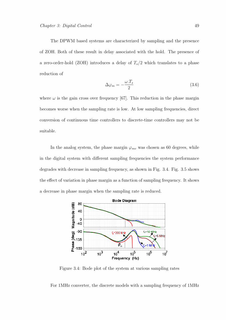
Chapter 3: Digital Control 49
The DPWM based systems are characterized by sampling and the presence
of ZOH. Both of these result in delay associated with the hold. The presence of
a zero-order-hold (ZOH) introduces a delay of Ts/2 which translates to a phase
reduction of
∆ϕm = −ω.Ts
2(3.6)
where ω is the gain cross over frequency [67]. This reduction in the phase margin
becomes worse when the sampling rate is low. At low sampling frequencies, direct
conversion of continuous time controllers to discrete-time controllers may not be
suitable.
In the analog system, the phase margin ϕmv was chosen as 60 degrees, while
in the digital system with different sampling frequencies the system performance
degrades with decrease in sampling frequency, as shown in Fig. 3.4. Fig. 3.5 shows
the effect of variation in phase margin as a function of sampling frequency. It shows
a decrease in phase margin when the sampling rate is reduced.
234
4
34
56789:;<=><?@
A4B
A4C
A43
A4D
A4E
A4F
2AG4
2ACD
2H4
IJ6K=><=7@
LMNOPNQRS TUVW
XYZN [\]^M]_G4
mϕ `abc def
`abcg def
`abh def`abigg jef
Figure 3.4: Bode plot of the system at various sampling rates
For 1MHz converter, the discrete models with a sampling frequency of 1MHz

Chapter 3: Digital Control 50
48
52
56
60
Phase Margin (Degrees)
105
106 10
7
Sampling Frequency(Hz)
Decreasing
Phase Margin
Figure 3.5: Effect of sampling frequency on phase margin of the compensatedsystems
with ZOH are given as:
Gvd(z) =vout
d=
0.0189z − 0.01199
z2 − 1.969z + 0.9704
Gikd(z) =iLk
d=
4.159z − 4.049
z2 − 1.969z + 0.9704
Gvi(z) =vout∑iLk
=9.398× 10⁻⁴z − 5.249× 10⁻⁴
z − 0.9734(3.7)
The ZOH delay compensated controllers are given as:
Cv(z) =365.5z − 271.4
z − 1
Cik(z) =0.3142z − 0.2869
z − 1(3.8)
The bode plots for the continuous and discrete-time designs given in Fig. 3.6.
Curve (a) shows the frequency response of the continuous time system, (b) is the
response of the digital control system.

Chapter 3: Digital Control 51
klm
m
lm
nopqrstuvwuxy
zm
zm|
zml
zm
zm~
kzm
kz|
km
ovwuvpy
zm|
zml
zm
zm~
zm
m
lm
m
nopqrstuvwuxy
kzm
km
ovwuvpy
Figure 3.6: Bode plots of the system obtained by different methods. (i) Inner Cur-rent Loop (ii) Voltage Loop with inner current loop closed. Curves: (a) Continuoustime system, (b) Digital control system
3.1.5 Current and Voltage Sensing
For current control, the inductor current needs to be sensed. Number of
methods have been proposed and implemented in the past [70]. Resistive sensing
is used for current control. The voltage across the sense resistor is expected to be
proportional to the current flowing through it. However, due to parasitic inductance
associated with the series resistance, the sensor output will not be proportional to

Chapter 3: Digital Control 52
the current. Thus a simple low-pass RC network is used to filter the voltage across
the sense-resistor. One such arrangement is shown in Fig. 3.7(a). For Rs + sLs ≪
R + 1/(sC), the voltage across the series-sense resistor is vsense = (Rs + sLs)IL,
where Rs is the resistance and Ls is the parasitic inductance associated with it.
The output of the sense amplifier is
vsa = Ksa.vc =Ksa.vsense1 + sRC
=Rs + sLs
1 + sRCIL (3.9)
vsa = Ksa.Rs1 + sLs/Rs
1 + sRCIL (3.10)
where Ksa is the gain of the sense amplifier. Hence, by ensuring RC = Ls/Rs, the
sensed voltage will be proportional to the inductor current (vsa = Ksa.Rs.IL).
iL
L
Ls
VC
Rs
R C
Sense Resistor
Vsense 0 2.5 5(ms)
Sense Amplifier (Vsa)
0
1V
2V
05A
10AInductor Current (iL)
Sense Amplifier
(a) (b)
iL
VsaVsaKsa
Figure 3.7: (a) Filtering the voltage across the sense resistor to eliminate the effectsof parasitic inductance and (b) Output of the sense amplifier and the inductorcurrent as measured using current probe.
Fig. 3.7 shows the current sensing circuit and its performance. The current
sensing ratio used is 0.15V/A. Since average current control is desired, the average
value of the inductor current can be obtained by sensing the current in the middle
of the switch-on and switch-off intervals. In this implementation, resistive sensing
is used along with the compensation for the parasitic inductance to sense the av-

Chapter 3: Digital Control 53
erage inductor current(s) by sampling in the middle of the on-time. However sense
resistance method is not very efficient for high current operations. The method
was used primarily to verify the control and is not a suggested method of current
measurement.
For sensing Vout, the output voltage is fed to an ADC. In order to eliminate
measurement noise, 8 samples are taken within a switching period and averaged
over the period to obtain Vout(k).
3.1.6 Controller Implementation
The control algorithm takes the sample of the output voltage Vout(k) and
the inductor current IL(k) and gives the duty ratio word D(k), which can be used
to generate the gate signals for various leaves. The block schematic of a digital
controller is shown in Fig. 3.8.
Power Stage
V out
Sense Amplifier
Sense Amplifier
Quantizer Quantizer
Voltage Loop Controller
Current Loop Controller
DPWM
MOSFET Drivers
To MOSFETs V out I L
V in
V ref
FPGA Board
I ref
Load
Figure 3.8: Schematic of digital controller design using FPGA
The controllers in eq. (3.8) are designed for a unity gain feedback. Including

Chapter 3: Digital Control 54
the gains of the sensing circuit, the compensator for the equivalent unity feedback
gain are:
Cv(z) =Iref (z)
Verr(z)=
54.83z − 40.71
z − 1
Cik(z) =D(z)
Ierr(z)=
1.351z − 1.233
z − 1(3.11)
The controllers obtained above are based on a first order polynomials. These
controllers can be re-written in the form of a difference equation. The output of the
voltage compensator will give the current reference, whereas the duty ratio will be
obtained from the output of the current compensator. Using the set of equations
in (3.11), the difference equations are obtained as:
Iref (k)− Iref (k − 1) = 54.83Verr(k)− 40.71Verr(k − 1)
D(k)−D(k − 1) = 1.351Ierr(k)− 1.233Ierr(k − 1) (3.12)
Since its a first order difference equation, it can easily be realized using direct
form of filter structure. Due to the fixed-point nature of the FPGA, a quantization
process has to be carried out for the controller coefficients. The quantization pro-
cess depends on the required precision of the filter coefficients. Such a quantized
filter will dictate the word-length requirement for implementation.
Quantization of such a filter may lead to unstable systems when the poles
of the filter fall outside the unit circle. Sensitivity of pole-zero locations has been
widely studied for stability [67][71]. Though this gives the minimum word-length
for stability, it may not give word length requirement for the desired performance.

Chapter 3: Digital Control 55
For example, to implement the controller with a precision up to 2-decimal places,
the quantization and rounding off process will require multiplication and division
by 100. Since the controller has to be implemented on a digital platform, multipli-
cation or division by powers of 2 can be achieved by using shift operations. Hence
no hardware multipliers are necessary. Therefore, the eq. (3.12) is multiplied with
27 = 128 on both sides, as this is closest to 100. Similarly for quantizing the
coefficients up to third decimal place, the equation is multiplied by 210.
In general, for obtaining a precision up to n-decimal places, the coefficients
are multiplied with 2k, where k is given as:
k = round(log2(10n)) (3.13)
0 2 4 6 8 10 12 14 16 18
58
46
48
50
52
54
56
Number of bits allocated for decimal part (k)
Pha
se M
argi
n ob
tain
ed(d
egre
es)
unstable
Figure 3.9: Effect of truncation on the filter coefficients in current controller
Fig. 3.9 shows the effect of truncation of the filter coefficients in current
compensator. It can be clearly seen that for k ≥ 6 bits, the performance of the
system is not improved much. Using eq. (3.13), 6-bits for the decimal part means
the coefficients are used with a precision of 10−2.

Chapter 3: Digital Control 56
Multiplying the equations using k=6 and rounding off the coefficients to the
nearest integer, the difference equations are obtained as
Iref (k) = [55Verr(k)− 41Verr(k − 1)] + Iref (k − 1)
D(k) = 2−6[86Ierr(k)− 78Ierr(k − 1)] +D(k − 1) (3.14)
A filter structure as shown in Fig. 3.10 is used.
z -1
55
Ve(k) Ve(k-1)
41
z -1
Iref(k)
I'ref(k-1)
+
-+
z -1
86
Ie(k) Ie(k-1)
78
z -1
D(k)
D'(k-1)
+
-1
Vref(k)+
Vout (k)
-
IL(k)
+ -
8
8
8
14
142-6
8
2-6
9
15
+
15
15814
I'ref(k) D'(k)
81
Figure 3.10: Direct Form : Filter realization
In the above realization, if the same truncation process is used for both the
controllers, this controller will require 21-bit implementation, where 12-bits repre-
sent the coefficients, 1 bit for the sign and 8-bits for representing sampled signal.
Different precision is used for the voltage and current controllers without degrad-
ing the performance. While the current controller is normalized by 26, the voltage
controller is obtained by rounding off to give a coefficient format that is multi-
plied by 20. Thus for a 9-bit resolution in the duty ratio, these controllers can be
implemented conveniently with 15-bit word size.

Chapter 3: Digital Control 57
3.1.7 Stability Analysis
If the above system is realized using a difference equation, then it is clear that
the pole nearest to the unit circle will be most sensitive to change in coefficient. The
pole-zero sensitivity was studied to obtain the allowable change in the coefficients
so as to have a stable system.
For a characteristic equation of the form
zn + α1zn−1 + ...+ αn = 0 (3.15)
which has roots λ1, λ2..., λn, the sensitivity of the roots due to change in coefficients
can be obtained as in [67]
δλj = −λn−kj∏
l 6=j(λj − λl)δαk (3.16)
For example, the inductor current to duty ratio transfer function and the
current controller is defined as
Gikd(z) =4.159z − 4.049
z2 − 1.969z + 0.9704
Cik(z) =Az + B
z − 1(3.17)
The characteristic equation of the closed current loop can be obtained as
z3 + (4.159A− 2.969)z2 + (2.939− 4.049A+ 4.159B)z + (−4.049B − 0.9704) = 0.
The poles of the closed inner loop are located at z1 = −0.21675, z2 = 0.90505
and z3 = 0.97385. Thus a change in the coefficient by (1− 0.97385) will move the

Chapter 3: Digital Control 58
pole to the unit circle and lead to instability. Hence the sensitivity of coefficients
of the characteristic polynomial is given as δα1 = −0.30271, δα2 = −0.31083 and
δα3 = −0.31918. These changes correspond to the following changes in coefficients
A and B of our current controller as defined in eq. (3.17),
∆A ≤ 0.0727,∆B ≤ 0.0788 (3.18)
Thus, in order to maintain a stable system, the change in coefficients should satisfy
eq. (3.18). Thus the number of bits required for such sensitivity can be obtained
as log2(min(∆A,∆B)) = 4 bits.
This can be verified from Fig. 3.9, which shows the effect of truncation of
the filter coefficients. As seen from the Fig. 3.9, the system is unstable if less than
4-bits are allocated for the fractional part. But keeping the system stable is not
sufficient. We need to obtain the desired performance as well. If more than 6-bits
are allocated for the fractional part, there is no significant improvement on the
system performance. Thus the compensator can be obtained by normalizing with
2−6.
Similarly the location of closed voltage loop poles can be obtained as z1 =
0.97344, z2 = 0.91148, z3,4 = 0.8926 ± i0.1493 and z5 = −0.4835. Clearly, the
pole located close to the unit circle will be most sensitive to coefficient change.
For this to happen, the compensator coefficients A and B should change by ∆A ≤
7.45,∆B ≤ 1.67. Thus, the voltage compensator can be obtained by rounding off
process.

Chapter 3: Digital Control 59
Figure 3.11: Photograph of the prototype of a 4-phase interleaved converter devel-oped in the lab
3.1.8 Digital Dither
It has been shown that [17], if the resolution of ADC is greater than the
resolution of the digital PWM (DPWM) counter and there is no integral control
action, a limit cycle oscillation occurs. Therefore, it has been recommended that the
resolution of DPWM be at least 1 bit higher than that of ADC. Digital dithering
technique is used to improve the resolution of the DPWM modules, where the
resolution of the DPWM counter is lower than the resolution of the ADC. It involves
varying the duty cycle by an LSB over a few switching cycles, such that intermediate
sub-bit level duty ratios are achieved. This is illustrated in Fig. 3.12(a). Here D
and (D+1) are the adjacent quantized duty ratios from the DPWM counter. If the
duty ratio is allowed to alternate between D and (D+1), an average duty ratio of
D+(1/2)LSB is achieved. This realizes (1/2)LSB DPWM level which is equivalent

Chapter 3: Digital Control 60
to an increase in resolution by 1-bit. This concept can be extended further to
achieve 2-bit effective increase in DPWM resolution. In such a scheme, (D + 1) is
introduced once every four switching periods, as shown in Fig. 3.12(b). Doing so,
(1/4)LSB DPWM levels are obtained which is equivalent to an increase in DPWM
resolution by 2-bits. It may be noticed that various dithering patters are possible,
but not all will result in same improvement in resolution. For example, if two out
of four switching periods are dithered, it will result in (1/2)LSB DPWM levels.
Likewise, if all the switching periods are dithered, it will not result in an improved
DPWM resolution as the overall duty ratio is increased to (D + 1). Thus, for a
2-bit increase in effective resolution, dither patterns of (1000), (0100), (0010) or
(0001) may be used.
Figure 3.12: (a) Switching waveform patterns to realize 1-bit dither; (b) Switchingwaveform patterns to realize 2-bit dither.
Fig. 3.13 shows some of the switching waveform patterns for 3-bit dither se-
quence. When (D+1) is introduced once every eight switching periods, (1/8)LSB

Chapter 3: Digital Control 61
DPWM levels are obtained which is equivalent to an increase in DPWM resolu-
tion by 3-bits. For a dither sequence, there may be a different patterns which
result in same improvement in DPWM resolution. For example, a dither pattern
of (11000000), (10100000), (10001000) etc will result in a sub-DPWM level of (2/8)
LSB. While (11000000) has lower fundamental frequency and thus produces higher
output voltage ripple, (10001000) will produce a lower ripple and have high fun-
damental frequency. Thus, it is also important to select the dither pattern which
results in low output voltage ripple.
Figure 3.13: Switching waveform patterns to realize 3-bit dither.
3.2 Experimental Results
Fig. 3.11 shows the photograph of the prototype of the 4-phase interleaved
converter. Due to large rate of change of the inductor current, it becomes necessary
to reduce the stray inductances. A parasitic inductance at the input side results in

Chapter 3: Digital Control 62
an overshoot in the switch voltage (Vds) during its turn-off. Due to the parasitic
inductance, the overshoot in Vds of the top-side MOSFET was obtained as 6.9V,
when the current is switched off from 24A to 0A in 11.2ns. The parasitic inductance
can be calculated as 3.2nH. This overshoot results in higher switching losses, which
forms a major component of total losses especially in the converters operating at
high switching frequencies. Effort can be made to reduce the stray inductance of
the circuit, but it gets limited by the package inductance. Typical stray inductance
of a TO-220 package at 1MHz is 12nH, D2-PAK(TO-263) offers around 5nH and
D-PAK(TO-252) offers around 2.5nH of package inductance [72]. Hence D-PAK
MOSFETs were chosen for this design and effective input side inductance was
observed to be 3.2nH. Package inductance of D-PAK(TO-252) alone will result in
an overshoot of 5.8V and in our case an overshoot of 6.9V was observed.
¡
¢£
¤£
¥£ ¦§¨©§¨ ª§««¬¨ ®¯¡
¦§¨©§¨ °±²¨³´¬ °¯µ¶¡
·¸°
¹·°
º»§¼¨±« ª§««¬¨
¹£
¢£
®¯
®½¾
®½¿
®½À
°¯µ¶¹·¸°
¢·¸ ¸
¢¹¸° ¹Á¸°Á£
Figure 3.14: Result showing the dynamic response of digitally controlled 4-phaseinterleaved converter for a step load variation from 15A to 70A
The controller performance was tested on the 4-phase interleaved buck con-
verter prototype with the following parameters: Vin = 5V , Vref = 1.25V , L =
1.2µH, fs = 1MHz per phase. In the prototype, the ADC had 8-bit resolution
and DPWM had 6-bit of hardware resolution. Thus, 3-bit digital dither was intro-

Chapter 3: Digital Control 63
duced to increase the effective resolution of DPWM module to 6+3=9 bits. The
calculated duty ratio was incremented by one, once every eight switching periods.
This achieves a DPWM level of (1/8)LSB which is equivalent to an increase in
DPWM resolution by 3-bits. The digital control algorithm has been implemented
on a Spartan-3 Field Programmable Gate Array (FPGA) by Xilinx. The system
was tested for load transients with a step-up change from 15A-70A and vice versa.
Fig. 3.14 shows the dynamic response of the controller, when reference voltage is
set as 1.25V. The load transients were generated by switching the load resistance.
The results shown above were to test the performance of the controllers. In
practice the VRM output requires adaptive voltage positioning (AVP). In adaptive
voltage positioning, the output voltage of the VRM is adapted to changes in the
load. This causes the output voltage to droop with the load. Adaptive voltage
positioning was implemented by changing the reference voltage in accordance with
the load current. Reference voltage is defined as
vref = Vref − io.Rdroop (3.19)
where Vref is the nominal reference voltage at no load conditions, io is the load
current and Rdroop is the droop resistance obtained from the load line. In AVP, the
output voltage is always positioned at a variable reference voltage vref , instead of
a fixed reference voltage Vref . Thus the converter behaves as a voltage source with
an output impedance of Rdroop.
Fig. 3.15 shows the dynamic response of the controller with adaptive voltage

Chapter 3: Digital Control 64
positioning with a droop resistance of Rdroop = 1.5mΩ. It shows a droop of around
100mV for a load change from 15A to 80A. The output settles to the new refer-
ence voltage without any overshoot, thereby showing good damping of the system.
Current sharing among various phases was also achieved during load dynamics.
0 250 500 (µs)
0
20A
40A
60AOutput Current (io)
Output Voltage (Vout)
0
0.5V
1.0V
Inductor Currents
0
10A
20A
io
iL1
iL2
iLk
Vout
1.5V
80A
Figure 3.15: Result showing the dynamic performance of the controller with adap-tive voltage positioning for a step load change from 15A to 80A
3.3 Summary
This chapter discussed the methods for obtaining the desired output voltage
regulation in VRMs. An interleaved converter topology is commonly used for
VRM applications. However, due to variations in component values among various
phases, it results in current mismatch among individual phase currents. To mitigate
this, controllers are designed for a 4-phase interleaved converter, which takes into
account the variations among individual inductor currents. The digital controllers
are designed taking into account the reduction in phase margin due to presence of
DPWM based ZOH. The effect of quantization of filter coefficients is also analyzed
and a minimum word length filter structure is proposed for such controllers.

Chapter 3: Digital Control 65
Table 3.1: Parameters of the interleaved buck converter prototype
N Number of Phases 4
Vin Input Voltage 5V
Lk Phase Inductors 1.2µH
Co Output Capacitor 5x470µF
Vref Reference Voltage 1.25V
∆Io Load Step 65A
Rdroop Droop Resistance 3mΩ
fs Switching Frequency 1MHz per phase
fsi Sampling Frequency of Inductor Current 1MHz
NADC ADC Resolution 8 bits
NDPWM DPWM Resolution 6 bit + 3 bit (dither)
fCLK System Clock Frequency 50MHz
The reduction of phase margin can be compensated in the controller design.
However, the output regulation still depends upon the resolution of the duty ratio.
The fine duty ratio either requires the switching frequency to be lowered or the clock
frequency to be increased. The next chapter discusses the DPWM architecture
and proposes to improve the time resolution of the gate pulses without having to
increase the clock frequency.

66
Chapter 4
Time Resolution of the DPWM
4.1 Introduction
The digital controllers employ a Digital Pulse-Width Modulator (DPWM)
to control the duty ratio of the gate pulses. However, the time resolution of the
DPWM output depends upon its clock frequency. In general, for achieving N-
bit resolution of the DPWM block, it needs to be clocked at 2N .fs, where fs is
the switching frequency of the converter. To meet, the high switching frequency
demand along with high resolution of DPWM, various methods have been proposed
in the past. Such methods above can be broadly classified into following categories:
• introducing a dither in the DPWM output [17],
• using a customized DPWM architecture e.g ring-oscillator-multiplexer scheme
[18], tapped delay-line [24], [25], etc,
• increasing the clock frequency [30].

Chapter 4: Time Resolution of DPWM 67
The schemes based on customized DPWM architecture results in increased
silicon area and power consumption, which is undesirable. On the other-hand,
the schemes based on DLL and counter-based DPWM are not scalable in nature
and provides resolution improvement only for a limited range. To this end, a
scheme is proposed which does not multiply the clock-frequency, requires a few
additional gates and is scalable in nature. The proposed scheme is also well suited
for integration with the existing DPWM schemes.
4.2 Proposed Scheme
A counter based DPWM scheme is easier to implement but its time resolution
gets limited by the clock edges. Unlike conventional counter based DPWM scheme,
we propose a hybrid approach to improve the DPWM resolution. In this scheme,
the processing is done in digital domain and a high resolution duty ratio word
(D(k)) is obtained from the digital compensator. The counter based DPWM block
handles the upper significant bits while the duty ratio correction block handles
the remaining lower significant bits. The duty ratio correction block adopts a fine
phase shift technique which can shift the input gate pulse by a fraction of clock
period. By delaying the turn-off instance of the gate pulses, the time resolution of
such pulses can be increased. The time resolution is now a function of the phase
shift introduced in the signal, instead of the clock edges. A combination of resistors
and a capacitors are used to provide a phase shift in the turn-off instances. The
required values of these components can be easily realized in silicon and is thus

Chapter 4: Time Resolution of DPWM 68
well suited for integration.
The basic principle of such a scheme and the typical waveforms are shown
in Fig. 4.1. The working of this scheme can be explained as following: The
PWM pulse obtained from DPWM is used to charge up an RC network. By using
appropriate values of R and C, the delay in such a system can be controlled. If
the input pulse is D, the shifted waveform is obtained as Dnew, which has the same
duty ratio as that of D. However, Dnew will have a shift introduced at both turn-
on and turn-off instances of the input gate pulse. To mitigate this, an OR gate is
used for D and Dnew. The output of the OR gate, Dout will have a shift in the
turn-off instance alone. This shift is a function of the R and C values and helps in
increasing the time resolution of the duty-ratio pulses. The improvement in time
resolution can be obtained by observing the RC charging waveform.
D
D
R
C INV
D
TCLK
INV
X
INV
VX
Dnew
Dnew
VTH
DoutDout=D + Dnew
tshift
Vdd
D
Figure 4.1: Schematic of the scheme for delaying the edges of the gate pulses

Chapter 4: Time Resolution of DPWM 69
Consider a pulse of magnitude Vdd charging the capacitor. The capacitor
voltage at time t is given as
vc = Vdd(1− e−t/RC) (4.1)
If the threshold voltage for the inverter is VTH , the time taken by capacitor voltage
to reach VTH can be obtained by solving
VTH = Vdd(1− e−t/RC) (4.2)
Thus, the time-shift in gate pulse is obtained as
tshift = −RC · loge(1−VTH
Vdd
) (4.3)
As a design example, we choose VTH = Vdd/2 and the shift is obtained as tshift =
0.693RC. In the conventional counter based DPWM block, the time resolution
of the PWM pulses is limited by the clock period. As a result, the duty ratio
resolution is TCLK . By choosing appropriate RC, the shift can be controlled such
that tshift = TCLK/2 and the time resolution can be improved to TCLK/2.
DPWM
D1
D2
D3
D
D D+ DD8-D2
D1D0Set D1=Tclk/4
Set D2=Tclk/2
Set D3=3Tclk/4
01
10
11
00D0
D’
EN
Duty
Ratio
Correction
S1S0
DPWM Resolution= Tclk
Update
Resolution= Tclk/4
Duty
Ratio
D8-D0
Used for finer
resolution
Dout
Used for coarse
resolution
Figure 4.2: Block schematic of the proposed scheme. The duty ratio is updatedbased on the least significant bits.

Chapter 4: Time Resolution of DPWM 70
4.2.1 Extending the scheme for finer resolution
The scheme presented above can be extended to obtain finer resolution. The
block schematic for improving the time resolution to TCLK/4 is shown in Fig. 4.2.
In such a scheme, the processing is done in digital domain and a high resolution duty
ratio word (D(k)) is obtained from the digital compensator. The counter based
DPWM block handles the upper significant bits while the duty ratio correction
block handles the remaining lower significant bits. The resolution of the duty ratio
word is increased using the state of the lower significant bits. Here, a 9-bit duty
ratio word (D8−D0) is obtained from the digital compensator. The DPWM block
handles the upper significant bits D8 − D2 and generates the pulses with coarse
resolution. The scheme then updates the PWM pulses with ∆D1, ∆D2 or ∆D3
depending upon the state of lower significant bits (LSB) D1D0. Here ∆D1, ∆D2
and ∆D3 are obtained according to the appropriate RC delays such that
∆D1 =1
4TCLK (4.4)
∆D2 =1
2TCLK (4.5)
∆D3 =3
4TCLK (4.6)
Doing so will obtain the time resolution of TCLK/4. It can be extended further
by increasing the size of duty ratio correction block. The detailed schematic of
the duty ratio correction block is shown in Fig. 4.3. A coarse duty ratio (D) is
obtained from the counter based DPWM block as described above. The duty ratio
correction block updates the PWM pulses with ∆D1, ∆D2 or ∆D3 depending upon

Chapter 4: Time Resolution of DPWM 71
the state of lower significant bits D1D0. Based on D1D0, only one of the shifted
pulses will be available which is used to obtain the finer resolution pulses as Dout.
The scheme shown above provides 4x improvement in time resolution. It
can be extended further by increasing the size of the duty ratio correction block.
However, the extent of duty ratio correction will depend upon the matching of
the resistances and capacitances for providing various time shifts. If the precise
matching is not available, laser trimming or factory calibration process can be used
for fine tuning the time shifts of duty ratio correction block.
In comparison, the proposed hybrid approach is similar to the delay-line and
a multiplexer based approaches. Such approaches use a number of delay cells to
realize a ring oscillator operating at the switching frequency. The power consump-
tion is governed by the number of delay cells and the switching frequency. Unlike
the other hybrid approaches, one delay cell is used at a time and the power to the
rest of the delay cells is shut down. Since only one of the delay cells in the duty
ratio corrector is used, it helps in reducing the dynamic power of the system.
4.2.2 Effect due to variation in component values
The proposed scheme uses resistors and capacitors to generate the shift in the
duty ratio pulse. However, in practice there will be variations in the component
values due to process mismatch. Thus, it is important to evaluate the effect of
process variations. It has been established that in order to achieve a time resolution

Chapter 4: Time Resolution of DPWM 72
(from DPWM)
R1
C1
INV
Vdd
D1D0
R2
C2
INV
D1D0
R3
C3
INV
D1D0
D
01
10
11
D1=TCLK/4
D2=TCLK/2
D3=3TCLK/4
Dout
Duty Ratio Correction
Vdd
Vdd
Figure 4.3: Detailed schematic of the proposed scheme. The duty ratio is updatedbased on the least significant bits.
of TCLK/2, we have
tshift = 0.693RC = TCLK/2 (4.7)
For a clock frequency of 50MHz, we may set C = 1pF and R = 14.43kΩ. The
effect on time-shift due to component variations is obtained as
∂tshift = 0.693(R · ∂C + C · ∂R) (4.8)
where ∂R and ∂C is the change in resistance and capacitance respectively. Thus
if there is ±5% variation in the component values, the worst case change in delay
will be ±2ns, which is within the desired resolution band of TCLK/2.

Chapter 4: Time Resolution of DPWM 73
(a)
(b) (c)
Time
1.0
0.8u 1.4u1.0u 1.2u
0.8
0.6
0.4
0.2
0Time
vc1vc2
vc3
Capacitor
Voltage
(V)
0
1.00
0.8u 1.4u1.0u 1.2u
0.50
D=20% D=22%
fclk=50MHz0.00
1.00
1.200u 1.220u
0.50
D=20% D=22%
fclk=50MHz
TCLK=20ns
Time
With D1
With D3
With D2
Figure 4.4: Simulation results showing the performance of the proposed scheme.(a) Resulting voltage waveforms at capacitors C1, C2 and C3; (b) The PWM pulsesobtained using the proposed scheme and (c) The 4 possible duty ratios generatedusing the proposed scheme.
4.3 Simulation Results
The performance of the scheme for obtaining finer duty ratio was tested on
Simplorer circuit simulator [73]. Fig. 4.4 shows the resulting waveforms. A clock
frequency of fCLK = 50MHz was chosen to demonstrate the concept. Such clock
frequencies are common on FPGA based development board and will provide a
time resolution of TCLK = 20ns. For 5V to 1V conversion, a typical duty ratio of
20% is produced. For a counter based DPWM, this corresponds to a duty ratio
command of D(k) = 10. A next higher duty ratio command is D(k) = 11, which
is equivalent to 22% duty ratio. By choosing the appropriate RC time constants,

Chapter 4: Time Resolution of DPWM 74
ÂÃÄÅ ÆÃÇÇ ÆÃÇÅ
ÂÃÆÅÇÇÇ
ÂÃÆÅÈÆÅ
ÉÊËÌ ÍËÎÏÂÃÄÇ
ÂÃÆÅÇÇÇ
ÂÃÆÅÈÆÅ
ÂÃÆÅÇÇÇ
ÂÃÆÅÈÆÅ
ÂÃÄÅ ÆÃÇÇ ÆÃÇÅ ÉÊËÌ ÍËÎÏÂÃÄÇ
ÂÃÄÅ ÆÃÇÇ ÆÃÇÅ ÉÊËÌ ÍËÎÏÂÃÄÇ
ÍÐÏ
ÍÑÏ
ÍÒÏ
ÓÔÕÖÔÕ×ØÙÕÚÛÜÝ×Þ
Figure 4.5: Simulation results showing the performance of three different controlmethods: (a) Analog control; (b)Conventional Digital Control and (c) ProposedController with duty ratio correction
a time resolution of TCLK/4 is obtained. Fig. 4.4(a) shows the resulting voltage
waveforms at different capacitors and the obtained duty ratio pulses are shown in
Fig. 4.4(b)(c).
The performance of the proposed control scheme was tested on a buck con-
verter with the following specifications: Vin = 5V , Vref = 1.25V , L = 1.2µH,
Co = 1000µF , fs = 1MHz. Three different control methods were simulated. The
system was subjected to a change in reference voltage in steps of 6.25mV, which
is equivalent to a change by 1 bit in a 7-bit VID word. The reference step was
given at t = 2ms. Fig. 4.5 shows the comparison of three schemes. As seen from
the results, the analog controller settles to new reference voltage in 10µs, while the
digital controller with 8-bit DPWM undergoes limit cycle oscillations due to poor

Chapter 4: Time Resolution of DPWM 75
resolution in time. On the other hand, the proposed controller with 8-bit coarse
and 2-bit duty-correction also settles to the new reference without any limit cycle
oscillations.
Voltage Loop
Controller
Current Loop
Controller
DPWM
Vref
Iref
KPV KIV KPI KII
DoutDuty Ratio
CorrectionD
D1D0
D1D0D
D8D2
CLK
Vdd
Vss
Vout(k)
IL(k)
Figure 4.6: Block schematic of the chip architecture
ßàßá
â
Figure 4.7: Micrograph of the fabricated ASIC, named DigResv1
4.4 Experimental Results
An Application Specific IC (ASIC) comprising of the digital controller and
the duty ratio corrector was fabricated in Austria Micro-Systems (AMS) 0.35µm
CMOS process. The chip architecture is shown in Fig. 4.6. It implements a

Chapter 4: Time Resolution of DPWM 76
current mode control for a single phase DC/DC converter. The output voltage and
inductor current are sampled using an external ADC. Five bit inputs are used for
the proportional and integral gains of the digital controllers, which can be set from
outside. The DPWM output and the two LSBs are brought out for monitoring
purposes. The chip also has a provision of testing the duty ratio corrector alone
externally supplying D and D1D0. Due to large number of test pins, the chip
area was limited by the required I/O cells. Fig. 4.7 shows the micrograph of the
fabricated chip. The digital core occupies an area of 877µm× 796µm, whereas the
duty ratio corrector occupies only 138µm× 200µm.
D(k)D(k+1)
TON(k)=200nsTON(k+1)=220ns
TON=201ns
D(k)D(k+1)
TON(k)=200nsTON(k+1)=220ns
TON=203ns
D(k)D(k+1)
TON(k)=200nsTON(k+1)=220ns
TON=210ns
D(k)D(k+1)
TON(k)=200nsTON(k+1)=220ns
TON=216ns
D1D0=00 D1D0=01
D1D0=10 D1D0=11
Time
ConventionalDPWM Outputs
RevisedDPWM Output
1µs 1.1µs 1.2µs0.9µs 1.4µs0V
1V
2V
3V
0V
1V
2V
3V
Time
ConventionalDPWM Outputs
RevisedDPWM Output
1µs 1.1µs 1.2µs0.9µs 1.4µs0V
1V
2V
3V
0V
1V
2V
3V
Time
ConventionalDPWM Outputs
RevisedDPWM Output
1µs 1.1µs 1.2µs0.9µs 1.4µs0V
1V
2V
3V
0V
1V
2V
3V
Time
ConventionalDPWM Outputs
RevisedDPWM Output
1µs 1.1µs 1.2µs0.9µs 1.4µs0V
1V
2V
3V
0V
1V
2V
3V
(a) (b)
(d)(c)
Figure 4.8: Experimental results showing the variation of duty ratio in accordancewith duty-ratio correction command (D1D2)
For a controller working with 50MHz clock, the duty ratio resolution is TCLK

Chapter 4: Time Resolution of DPWM 77
(=20ns). In order to test the functionality of the duty ratio correction block,
a 1MHz clock with a duty ratio of 20% (TON = 200ns) is generated using an
FPGA board and is given as an input (D). The next higher duty ratio of 22%
(TON = 220ns) is also captured for reference. As expected the time separation
between D(k) and D(k + 1) is observed as 20ns. With D(k) as an input to the
duty ratio corrector, the correction command (D1D0) is varied and the revised
DPWM output observed for the given 4 cases (D1D0 = 00, 01, 10 and 11). Fig.
4.8 shows the corrected duty ratio pulses. For an input ON period of 200ns, the
ON periods of 201ns, 203ns, 210ns and 216ns are obtained which are quite close
to the expected durations of 200ns, 205ns, 210ns and 215ns. As seen from the
experimental results, a resolution of TCLK/4 (=5ns) is obtained which is 4-times
improvement over the conventional scheme.
64-pin LQFP
packaged chip
Switches to set the
P and I gains
ADC: Voltage
Sampling
ADC: Current
Sampling
Figure 4.9: Experimental prototype of the controller realized using the fabricatedASIC and the off-chip ADCs
Chapter 4: Time Resolution of DPWM 78
The above experiment was to test the duty-ratio corrector alone. However,
a digital controller was also integrated on the same chip which is used to generate
the gate pulses for a DC/DC converter. Fig. 4.9 shows the controller prototype
realized using the fabricated ASIC. Two off-chip 8-bit ADCs with a dynamic range
of 3.3V were used to sample the output voltage and the inductor current. The
proportional and integral gains of the digital controllers were set using external
switches. To emulate the VID code, the 7-bit reference Vref is set from outside
and the functionality of the chip was tested on a buck converter with the following
specifications: Vin = 5V , L = 1.2µH, Co = 1000µF , fs = 1MHz and fCLK =
50MHz. The conventional scheme is realized by directly using the output from
digital core. For realizing the proposed scheme, the DPWM output is connected to
the duty-ratio correction block and the output of correction block is used as gate
pulses. The VID is varied and the output voltage regulation is observed in these
two cases. Fig. 4.10 shows the output voltage obtained in the two cases. As seen
from the figure, the proposed scheme reduces the voltage regulation error resulting
due to the finite time-resolution of DPWM.
0
0.2
0.4
0.6
0.8
1.0
1.2
1.4
1.6
0 20 40 60 80 100 120VID Code
Out
put V
olta
ge (
V)
05
1015202530354045
0 20 40 60 80 100 120VID Code
Err
or R
educ
tion
(%)
Using ConventionalDPWM
Using ProposedDPWM
Ideal Case(econventional)-(eproposed)
Figure 4.10: Experimental results the output voltage regulation for proposed caseand conventional case.

Chapter 4: Time Resolution of DPWM 79
4.5 Summary
This chapter has identified the challenges in achieving fine resolution of duty
ratio when high switching frequency is required. Thus, it was proposed to improve
the time resolution of the PWM pulses by updating their turn-off instances. Using
such a scheme, the time resolution of analog domain and processing powers of
digital implementation can be combined. From the experimental and simulation
results, it is concluded that the proposed scheme is effective in improving the time
resolution of the DPWM output without having to increase the clock frequency.
The scheme was tested on a single phase buck converter with a current mode
control. A current controller requires the inductor current to be sensed. The
next chapter discusses the available current sensing methods and brings about the
advantages and disadvantages of various methods. It also proposes a new current
sensing method, which is suitable for VRM type applications.

80
Chapter 5
Giant Magneto Resistive (GMR)effect based Current SensingTechnique
5.1 Introduction
Almost all DC-DC converters sense the inductor current for various purposes.
Current sensing may be used for providing over-current protection. It may be used
in current-mode control of DC-DC converters for improving the transient response
of the closed loop system. Such current mode control may be based on average
current or peak current control. Current sensing may also be used for load sharing
among paralleled converters.
Numerous methods have been proposed and implemented for sensing the cur-
rent. All these current sensing techniques can be broadly classified as non-isolated
[34]-[37] and isolated sensing techniques [38]-[39]. The non-isolated methods men-
tioned above are either lossy or they rely on the component value. Methods based

Chapter 5: GMR Sensor 81
on SenseFET require special MOSFETs to be designed and they need to be properly
matched. The isolated methods are bulky and have poor temperature character-
istics. These methods are certainly not useful for high performance VRM type
applications where output currents are high and it is desired to maintain good
current sharing despite tolerances in component values. Thus, a current sensing
mechanism is required, which is independent of the value of external components,
provides temperature independent sensing accuracy and is practically lossless.
5.2 Proposed Method
5.2.1 Description
In this chapter, a new scheme for sensing and controlling the inductor current
is used. It is based on Giant Magneto Resistive (GMR) effect. GMR effect has been
used extensively in the read heads in modern hard disk drives. Another application
of the GMR effect is in non-volatile, magnetic random access memory (MRAM). In
this work, this method is used for sensing the inductor current in low voltage/high
current power supplies.
In GMR effect, a large change in electrical resistance occurs when thin,
stacked layers of ferromagnetic and non-magnetic materials are exposed to a mag-
netic field [74]. Fig. 5.1 shows the working principle of GMR effect using stacked
layers. Layer A which is a conductive, non-magnetic interlayer which is sandwiched
between two ferromagnetic layers B. Among various combination of materials used

Chapter 5: GMR Sensor 82
for forming these layers: Co, Fe, NiFe, CoFe and other alloys are used as ferro-
magnetic layers while Cr, Cu, Ag, etc are commonly used for the interlayer. The
magnetic dipole moments in adjacent ferromagnetic layers (B) are antiparallel due
to weak anti-ferromagnetic coupling between the layers. Thus the resistance offered
by the BAB stack to the current flowing through the stacked layers (IGMR) is high.
Applying an external magnetic field helps in over coming the anti-ferromagnetic
coupling, thus aligning the magnetic dipole moments in the alloy layer B along the
direction of magnetic field. This results in reduction of electrical resistance of the
BAB stack by 10% to 15%.
Fig. 5.1 shows the GMR effect when the current flow (IGMR) is perpendicular
to the plane of the layers. GMR effect is also observed when the current is in the
plane of the layers. The former is called current-perpendicular-to-plane, or CPP
sensor and the latter is called current-in-plane, or CIP sensor [75]. Usually the
GMR effect in CPP is higher than in CIP. In both the cases, the resistance offered
to the current flow can be reduced by applying external magnetic field. The mag-
netic field can be applied by using the current to be measured (Imeasure). Change in
current will change the magnetic field associated with the flow of current, thus caus-
ing the resistance to change. This change can be obtained by sensing the voltage
across the Wheatstone bridge, as shown in the Fig. 5.2. The Wheatstone bridge in
commercially available GMR sensors comprises of four identical multilayered GMR
resistors [76]. Two of the resistors (Rg) are surrounded by flux concentrators, while
the other two resistors are magnetically shielded, which allows them to act as base

Chapter 5: GMR Sensor 83
ã
ä
ã
ã
ä
ã
åæçèéêëì íëéîïïðé êñ ìðòòéèê óîñô
õðòòéèê íîñô
ö÷øù ö÷øùúëçûüéýëýêæèìé
þñôüéýëýêæèìé
ÿ õñèïðìêëèç ñèæçèéêëì îæéò õñèïðìêëèç íéòòñæçèéêëì îæéò
ñ åæçèéêëì íëéîï
ö÷øù
åæçèéêëìíëéîï þëèéý
õðòòéèêõæòòëèçõñèïðìêñò
æ! "! ì!
åæçèéêëì #ëñîéåñéèêý
Figure 5.1: Working principle of Giant Magneto Resistive Effect. (a) Higher re-sistance due to anti-parallel magnetic moments, (b) Paralleled magnetic momentsreduces the electrical resistance and (c) Cross section along XX’ plane showingalignment of magnetic moments due to magnetic field.
resistance (Rb). The output voltage from such an arrangement can be obtained as
Vsense =Rb −Rg
Rb +Rg
· Vcc (5.1)
The base resistance (Rb) is fixed and it does not change with change in magnetic
field. However, the resistance Rg changes with magnetic field. The sensitivity of
sensed output to the change in resistance Rg can be obtained as
∂Vsense
∂Rg
= − 2 ·Rb
(Rb +Rg)2· Vcc (5.2)
Thus the Wheatstone bridge configuration can amplify the small change in
resistance (Rg). The typical resistance offered by GMR is around 5 kΩ. The fixed
resistance is also designed to be the same. Thus when operating at 12V power
supply, it will result in a power consumption of 28.8mW . This power consumed is
practically independent of the current to be measured.
The Wheatstone bridge configuration in the commercially available GMR
sensors [76] also help in providing temperature compensation. The bridge uses

Chapter 5: GMR Sensor 84
OUT+
OUT-
Vcc
GMR
GMR
Vsense
IGMR
Rb
Rb
Rg
Rg
Magnetic
Shield
Magnetic
Shield
Flux
Concentrator
Flux
Concentrator
Figure 5.2: Wheatstone Bridge configuration available for sensing application.
four identical GMR resistors and all the resistors experience the same change in
resistance due to temperature change. This cancels out the inherent temperature
dependence [77]. Also, these ICs are sensitive in one direction in the plane of the
IC, with a cosine scaled fall-off in sensitivity as the sensor is rotated away from the
sensitive direction. These GMR sensors provide the same output for magnetic fields
in the positive or negative direction along the axis of sensitivity. These sensors are
characteriszed by high sensitivity to applied magnetic fields, excellent temperature
stability, practically low power consumption and small size. Thus they can be
suitable candidate for high current applications where resistive method can not be
used due to the associated power losses and other methods cannot be used due to
their complexity or the variations in the component values.
5.2.2 Work on Magnetoresistive effect
Anisotropic Magnetoresistance (AMR) property demonstrates the dependence
of electrical resistance on the angle between the direction of current flow and the

Chapter 5: GMR Sensor 85
orientation of magnetic field [78]. AMR effect has been used for current sensing in
[79]. However, with the advent of GMR technology, the AMR technology has been
surpassed. While the resistance change in AMR effect is approximately 2 − 4%,
the GMR offers change in resistance upto 10 − 15%. Magneto-Impedance (MI)
effect has also been explored which refers to the large variation of the impedance
of a magnetic material carrying an AC current when subjected to an external field
[38], [80], [81]. However due to its extremely high sensitivity, even small external
magnetic fields can induce a significant error. Thus, the accuracy of MI sensor is
highly susceptible to noise.
The GMR effect provides higher sensitivity than the AMR effect and is a
better candidate for sensing large range of currents. Unlike MI sensors, its does
not get significantly affected by small external fields. Thus due to their low cost,
small size and minimum temperature dependence, the GMR sensors can be an
alternative to the existing current sensors.
Although, the GMR sensors provide temperature compensation by using
wheatstone bridge configuration, a GMR based temperature sensing method has
been introduced in [77]. It decouples the temperature signal from the field mea-
surement by using one half of the wheatstone bridge. It relies on a constant current
supply as the bridge excitation. If a constant current source is applied, the volt-
age across the GMR elements will increase as the temperature increases. Such
a method is proposed for motor drive modules, with main focus on combining a
thermal sensor with the current sensor.

Chapter 5: GMR Sensor 86
The GMR sensor is based on the magnetic field generated by the current flow.
But the current density in a conductor depends upon its location in the cross-section
of the conductor and the frequency spectrum of the current. A study on influence
of eddy currents on magnetic field distribution due to closely lying conductors is
presented in [82]. It establishes an optimum location for accurately capturing the
entire spectrum of the current in motor drive applications. This is useful for point
field-based current sensing using an integrated GMR sensor, which does not have a
flux concentrator. However, in commercially available GMR sensors, the presence
of on-chip flux concentrators increases the field at the sensor elements. Moreover, in
switched mode power supply the AC component in the inductor current is designed
to be much smaller than the DC component. Thus it is important to note the DC
magnetic field distribution. In this paper, the optimum location for the magnetic
field detector is established for average current sensing based on DC magnetic field
distribution.
5.2.3 Magnetic Field distribution due to current carryingtrack
The work on GMR sensor is based around the commercially available GMR
sensors [76]. The technical information provided by the manufacturer assumes the
width of the current carrying track to be smaller than the IC width. However, for
high current applications, the track widths are designed to be wider than the IC
width. Thus, it is important to assess the performance of the sensor in these cases
for high current applications. To this end, a mathematical framework was devel-

Chapter 5: GMR Sensor 87
oped for correct positioning of the field sensor and to obtain its optimal response.
As mentioned earlier, the GMR sensor is based on magnetic field associated
with the flow of current. The magnetic strength will depend upon the distance
from the current carrying conductor. For example, the magnetic field density at a
distance r due to current carrying wire is given as
B =µoi
2πr(5.3)
where i is the current (in amperes) flowing though the wire and µo is the perme-
ability constant of free space (µo = 4π10−7 Tm/A). The farther the conductor, the
weaker is the magnetic field. Thus the placement of the sensor with respect to the
current carrying conductor becomes very critical. The magnetic field density can
be studied to obtain the variations in the sensed output with change in position of
the sensor.
z
y
x
x
dx
x
z
x
dx
x
y
ydy
W/2
-W/2 W/2Q(x,y,0) Q
P(a,b,c)
ds
r
dsI
CurrentFlow
PCBTrack
-W/2
Figure 5.3: Magnetic field at point P due to a long current carrying PCB track.
The magnetic field density due to current carrying track can be obtained with
the help of following analysis. Consider a long current carrying track in x-y plane,
with its current flowing in y-direction as shown in Fig. 5.3. The track thickness is

Chapter 5: GMR Sensor 88
assumed to be negligible as compared to other dimensions and is neglected. The
magnetic field due to this current carrying track can be obtained at any arbitrary
point having coordinates P(a,b,c). The magnetic field density due to an infinitesi-
mal current carrying element ( ~ds) carrying a current di located at Q(x,y,0) is given
as
~dB =µo
4π
di ~ds× ~r
r3(5.4)
where ~r is the vector pointing from the current element at (Q) to the observation
point (P).
Since the track is long enough, the point P is assumed to be in x-z plane.
Thus, the coordinates of point P can be simplified as P(a,0,c). Current flowing in
element at Q is di = IWdx, where W is the width of the track. The current element
orientation is ~ds = dyj and the distance of current carrying element from the point
under observation (P) is given as
~r = ~QP = (a− x)i− yj + ck (5.5)
where i, j and k are unit vectors along x, y and z-directions respectively.
This gives us the magnetic field density at P due to current carrying element
Q as
~dB =µo
4π· IdxW
ci+ (x− a)k
(c2 + (x− a)2 + y2)3/2dy (5.6)
The magnitude of this magnetic field density at P is obtained as
|dB| = µo
4π· IdxW
(c2 + (x− a)2)1/2
(c2 + (x− a)2 + y2)3/2dy (5.7)

Chapter 5: GMR Sensor 89
The GMR sensor has its axis of sensitivity along the x-y plane, while it is
insensitive to z-component of magnetic field. As obtained in (5.6), there is no
y-component of the field. Thus the total field in x-direction can evaluated by
integrating (5.6) over the track area.
Bx =
∫ x=W/2
x=−W/2
∫ y=∞
y=−∞
µo
4π· I · dx
W
c
(c2 + (x− a)2 + y2)3/2dy (5.8)
Rearranging the terms we get
Bx =µo
4π
I
W
∫ W/2
−W/2
∫ ∞
−∞
c · dy(c2 + (x− a)2 + y2)3/2
· dx (5.9)
Bx =µo
2π
Ic
W
∫ W/2
−W/2
dx
((a− x)2 + c2)1/2(5.10)
Bx =µo
2π
I
W[tan−1(
a+ W2
c)− tan−1(
a− W2
c)] (5.11)
Using (5.11), the general expression of the magnetic field at any arbitrary
point P(x,0,z) can be obtained by substituting a=x and c=z.
Bx =µo
2π
I
W[tan−1(
x+ W2
z)− tan−1(
x− W2
z)] (5.12)
The magnitude decreases as one moves away from the current carrying track
in the vertical direction. For a fixed height above the current carrying track, Bx
will be maximum when dBx
dx= 0. Clearly, the magnitude of the magnetic field
density will be maximum at x = 0. The field decreases as one moves away from
the center of the current carrying track and it attains the minimum as x → ±∞.
The field distribution obtained using above analysis was plotted using MAT-
LAB [83]. The results were verified using a 2-D finite element based field simulator

Chapter 5: GMR Sensor 90
$ %& '() * ++&, $ '()
') '-)
./ 0 /.1
0
1
*
./ 0 /
.1
0
1
*
10234
.5678
16/8
/680
10234
96/8
8600
5678
/680
16/8
0600
.16/8
./680
.5678
.8600
.96/8.96/8
96/8
.8600
./680
.16/8
0600
5678
8600
Figure 5.4: (a) Magnetic Field Distribution as obtained from MATLAB (b) Mag-netic Field Distribution as obtained from QuickField.
QuickField [84]. Fig. 5.4 shows the field distribution using two methods. The
current flow in both cases is set as 10A and the track width is 1 cm. Notice a good
agreement between the field patterns obtained by these two methods. The accu-
racy of the field distribution obtained in simulation depends upon the grid size.
The coarse grid size in QuickField (student version) resulted in small mismatch
in the two field patterns. This field pattern can be used to optimally place the
sensor for desired accuracy in field sensing. To this end, various sensor placement
configurations were studied and results are presented here.
5.2.4 Performance Evaluation
Fig. 5.5(a) shows an GMR magnetic field sensor (AA003-02 [76]) with its axis
of sensitivity along the horizontal direction. In order to study the performance,
the sensor was placed on the top of the PCB board and current was varied through

Chapter 5: GMR Sensor 91
the track made on the bottom layer of PCB. The track width was W = 5.5mm
and the supply voltage (Vcc) was kept at 20V. Fig. 5.5(b) shows the input-output
characteristics of such a sensor. Fig. 5.5(c) shows the linearity of output voltage
when the supply voltage was varied, while the current to be measured (Imeasure)
was kept constant. It shows the sensing gain varies linearly with the supply voltage.
The supply voltages of 15V∼20V are common in gate drivers and can also be used
to power these sensors.
The sensor was also studied to verify the temperature independence. ETAC’s
HISPEC high temperature chamber was used to control the temperature. The
PCB board having the GMR sensor was placed in the temperature chamber and
current was forced through the PCB track. The sensor output was noted for various
currents at various temperatures. Fig. 5.6 shows the input-output characteristics
at two different temperatures, T = 30oC and T = 70oC. It shows the sensing
accuracy in these sensors is temperature independent.
As established earlier, the farther the conductor is, the weaker is the magnetic
field. To study this effect, the current was made to flow through the bottom layer,
while the sensor was placed on the top layer (Fig. 5.7(a)). In another set, the
current was made to flow through a conductor lying on the sensor (Fig. 5.7(b)).
In both these cases, the track or conductor width was same as the sensor width.
Fig. 5.7(c) shows the output voltage obtained by these two configurations. It can
be seen that configuration B records a steeper input output characteristics. In
another study, a wider track was used and two sensors were placed, one in the
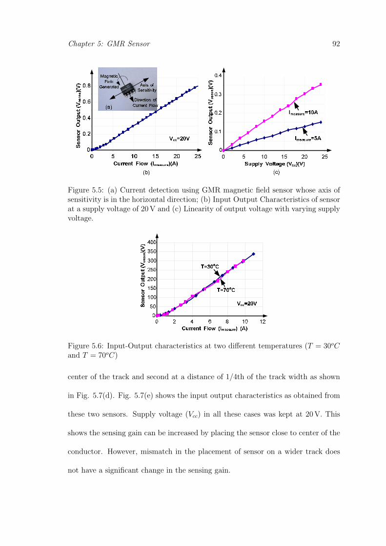
Chapter 5: GMR Sensor 92
:;<<=>? @ABC DEFGHIJKGLDML
NOPQRSTUVWUVXYZ[\Z[]XY]
^_`
abbcdea
f
fgh
fgi
fgj
fgk
l m nl nm ol om
pqrstuvwxvtyz
tst|qutz ~v tsvuvvu
v|twuvs ||tsu xy^`
;A aBA?= DabbLDaL
NOPQRSTUVWUVXYZ[\Z[]XY]
EFGHIJKGcM
EFGHIJKGceM
^`
Figure 5.5: (a) Current detection using GMR magnetic field sensor whose axis ofsensitivity is in the horizontal direction; (b) Input Output Characteristics of sensorat a supply voltage of 20V and (c) Linearity of output voltage with varying supplyvoltage.
¡
¡ ¢ £
¤¥¦¦§¨© ª«¬ ®¯°±²³´µ±¶ ®·¶
¸¹º»¼¤
¸¹½»¼¤
¾¿ÀÁÂÃÄÅÆÇÅÆÈÉÊËÌÊËÍÈÉÍ
ÎÏϹлÎ
Figure 5.6: Input-Output characteristics at two different temperatures (T = 30oCand T = 70oC)
center of the track and second at a distance of 1/4th of the track width as shown
in Fig. 5.7(d). Fig. 5.7(e) shows the input output characteristics as obtained from
these two sensors. Supply voltage (Vcc) in all these cases was kept at 20V. This
shows the sensing gain can be increased by placing the sensor close to center of the
conductor. However, mismatch in the placement of sensor on a wider track does
not have a significant change in the sensing gain.

Chapter 5: GMR Sensor 93
ÑÒÓ
ÔÒÕÕÒÖ
×ØÙÚÛÜ
ÝÞß
ÑÒÓ
ÔÒÕÕÒÖ
ÞàÜÜØÙá âãÛä åæçèéêëìèí
×ØÙÚÛÜÝÞß
×ØÙÚÛÜ î×ØÙÚÛÜ ï
ÞÛÙðñòàÜóáñÛÙ ô ÞÛÙðñòàÜóáñÛÙ ß ÞÛÙðñòàÜóáñÛÙ Þåóí åõí åöí
åØí
ÞàÜÜØÙá âãÛäåæçèéêëìèí
åæçèéêëìèí
å÷í
ÞÛÙðñòàÜóáñÛÙ ô
ÞÛÙðñòàÜóáñÛÙ ß
ø
ïøø
ùøø
úøø
ûøø
îøøø
îïøø
îùøø
ø ü îø îü ïø ïü
åýýþúïú ÿ#&ôí
åüùþúýû ÿ#&ôí
ÞàÜÜØÙá âãÛä åæçèéêëìèí åôí
×ØÙÚÛÜ ï
×ØÙÚÛÜ î
ÞÛÙðñòàÜóáñÛÙ Þ
ÞàÜÜØÙá âãÛä åæçèéêëìèí åôí
ø
üø
îøø
îüø
ïøø
ïüø
ýøø
ýüø
ùøø
ø ü îø îü ïø ïü
åîïþûýù ÿ#&ôí
åîýþüüý ÿ#&ôí
ÞàÜÜØÙá âãÛäåæçèéêëìèí
ÞàÜÜØÙá âãÛäåæçèéêëìèí
×ØÙÚÛÜ
Figure 5.7: (a) Current flow through the bottom layer; (b) Current flow through aconductor placed on top on sensor; (c) Output voltage as obtained from configu-rations A and B; (d) Placement of sensors on a wider track; and (e) Input Outputcharacteristics as obtained from configuration C.
This phenomenon can be explained with the help of the magnetic field density
obtained in (5.12). The sensing ratio in configuration A (Fig. 5.7) is 33.626mV/A,
while for configuration B it was observed as 54.638mV/A. This shows the sensor
records a higher magnetic field in configuration B. Based on this, the location of
sensor in the IC can be obtained. Lets say it is located at a distance of zB from
the top surface in configuration B and it is at a distance of zA from the bottom
surface, as shown in Fig. 5.8. zA + zB includes the PCB thickness (1.6mm) and
the height of the sensor in SOIC8 package (1.55mm). Thus,
zA + zB = 3.15mm (5.13)

Chapter 5: GMR Sensor 94
!" $
%
'(
')
*
*+
*
*+*
*+
!"
,-./0123
456/7
Figure 5.8: Determining the location of physical sensor in the Sensor chip.
Since the sensors are placed at the center of the track, x can be set as x = 0. Using
the ratio of these sensing gains, we have,
(WA
WB
)[tan−1(WB
2zB) + tan−1(WB
2zB)
tan−1(WA
2zA) + tan−1(WA
2zA)] =
54.638
33.626(5.14)
where WA and WB are the track widths for configuration A and B respectively.
The width of tracks used in configuration A and B is WA = WB = 5.5mm.
Solving (5.14) results in zA = 2.522mm and zB = 0.628mm. This allows us to set
z = 2.522mm in (5.12) for further analysis, when the current is flowing through
the layer lying under the PCB board having a thickness of 1.6mm and the sensor
is in SOIC8 package. Substituting z = 2.522mm in (5.12), we get
Bx =µo
2π
I
W[tan−1(
x+ W2
2.522× 10⁻³)− tan−1(
x− W2
2.522× 10⁻³)] (5.15)
Clearly the field is maximum in the plane lying along the center of the track (x = 0).
The maximum field is obtained as
Bmax =µo
π
I
W[tan−1(
W2
2.522× 10⁻³)] (5.16)

Chapter 5: GMR Sensor 95
Since the sensor output voltage is proportional to the magnetic field, we have
vsense = αv · Bx =
αv ·µo
2π
I
W[tan−1(
x+ W2
2.522× 10⁻³)− tan−1(
x− W2
2.522× 10⁻³)] (5.17)
where αv is the proportionality constant. Simplifying (5.17), we get
αv =vsenseI
2πW
µo[tan−1(x+W
2
2.522×10⁻³ )− tan−1(x−W
2
2.522×10⁻³ )](5.18)
Using the data from configuration A (W=5.5mm, sensing ratio=33.626mV/A),
the proportionality constant is obtained as αv = 557.9859V/Tesla. Using this, the
sensing ratio is calculated as
K =vsenseI
= 557.9859 · µo
2πW[tan−1(
x+ W2
2.522× 10⁻³)− tan−1(
x− W2
2.522× 10⁻³)] (5.19)
where W is the width of the track and x is the distance of the sensor from the
center of the track.
For configuration C, the track width was WC = 23.0mm. While sensor 1 was
placed along the center of the track and the sensor 2 was placed at a distance of
1/4th of the track width. Using (5.19), the sensing ratios for these two cases can
be obtained. The sensing ratio for sensor 1 can be obtained as 13.148mV/A and
for sensor 2 it is obtained as 12.533mV/A. The predicted values using the above
analysis match with the experimental values of 13.533mV/A and 12.834mV/A
respectively, as obtained from input-output characteristics in Fig. 5.7.
Although configuration B gives higher sensing ratio, it would require routing
the current over the sensor IC. Thus configuration A was chosen for further analysis,

Chapter 5: GMR Sensor 96
89:: 8;: 8<: 8=: 8>: : >: =: <: ;: 9:::
9
>
?
=
@
A 9:BC
DEFGHIJKLJHMNOPHQMER
STUVWXYZ [\]^ V_Z T` aZ ][ V_Z V\WYb cAd c^ d
cWd
: 9: >: ?: =: @: <: e: ;: f: 9:::
9:
>:
?:
=:
@:
<:
e:
;:
f:
9::
STUVWXYZ [\]^ V_Z T``aZ ][ V_Z V\WYb cAd c^ d
ghijEMJkHNjEFGHIJKLJHMNOlR
cmd
no>Y^
no9Y^
no=Y^
no?Y^
no@Y^no>Y^
no9Y^
no?Y^
no=Y^
no@Y^
Figure 5.9: Curves showing magnetic field distribution for varying track widthscarrying a current of 10A.
as it can be realized using conventional PCB design. Based on the magnetic field
distribution for configuration A, the magnetic field can be obtained as the point
of observation moves away from the track. Thus, x is varied in (5.15) for different
values of track widths. The current flowing through the track is 10A in each case.
Fig. 5.9(a) shows the magnetic field as a function of distance from the center of
the current carrying track. As expected, the peak magnetic field occurs at the
point lying above the center of the track. Using (5.15) and (5.16), the normalized
magnetic field is obtained as the ratio of magnetic field at a distance x from the
center of the track (Bx) to the maximum field for the given track width (Bmax). Fig.
5.9(b) shows the normalized magnetic field as one moves away from the current
carrying conductor.
Since the sensor is based on the magnetic field generated from the current
carrying conductor, the sensed output depends upon the location of the sensor. For
a reasonable accuracy of 90% or above, it would be interesting to note the range of

Chapter 5: GMR Sensor 97
location which can give the desired accuracy. Using the normalized magnetic field,
one can obtain the distance from the conductor for the desired accuracy. Fig. 5.10
shows the location of points from the center of the track where the magnetic field
reduces to 90% of its peak value, Bmax. This is marked by region 1© in Fig. 5.10.
Similarly, the field strength reduces to less than 10% in region 2©. This shows if a
second sensor is placed in region 2© for sensing the current in another conductor,
it will get influenced by the field due to first conductor. This gives us the distance
(x) where the sensor should be placed with respect to the track to achieve the
desired accuracy. For 90% or more accuracy it should be placed in region 1©, such
that 0 ≤ x ≤ x1. In order to reduce the interference to less than 10% among
closely lying sensors, they should be separated by a distance such that x ≥ x2. For
example, the track thickness of 20mm provides x1 = 6.4mm and x2 = 16.8mm.
Thus for an accuracy of 90%, the sensor should not be farther than 6.4mm from
the center of the track.
5.3 Experimental Results
The performance of the proposed method for current sensing was tested on a
buck converter prototype with the following parameters: Vin = 5V , Vref = 1.25V ,
L = 1.2µH, Co = 1000µF , fs = 1MHz. Fig. 5.11 shows the photograph of the
prototype of a buck converter which uses a GMR sensor. A wire loop is used to
probe the inductor current. AA003-02 was used for current sensing with its supply
voltage (Vcc) at 20V. The GMR sensor was placed on the top of the PCB board

Chapter 5: GMR Sensor 98
p q rp rq sp sq tp tq up uq qp
p
q
rp
rq
sp
sq
tp
tq
vwxyz |~ |
| rp
| p
r
s
¡¢
¡£
Figure 5.10: Curves showing the location of points where magnetic field reduces to90% in configuration A. Region 1© has magnetic field > 90% of Bmax and region2© has magnetic field < 10% of Bmax.
and current was made to flow through the bottom layer as in configuration A. The
output of the sensor was amplified before sampling it for control purpose. The
current sensing ratio used is 55mV/A. Since average current control is desired, the
average value of the inductor current can be obtained by sensing the current in the
middle of the switch-on and switch-off intervals. A digital controller was used to
obtain the desired performance of the system. The inductor current and the output
voltage was sampled using an ADC. The ADC had 8-bit resolution (NADC = 8) and
DPWM had 6-bit of hardware resolution. Thus, 3-bit digital dither was introduced
to increase the effective resolution of DPWM module to 6+3=9 bits (NDPWM = 9).
The controller was implemented on a Spartan-3 Field Programmable Gate Array
(FPGA) by Xilinx operating at a clock frequency of 50Mhz.
The dynamic response of inner current loop was studied to see the effect of
step change in the reference current. Fig. 5.12(a) shows the response of the system

Chapter 5: GMR Sensor 99
Q1 Q2
L
Wire loop to observe the
inductor current
Input
OutputGMR Sensor
Figure 5.11: Experimental prototype of a buck converter which uses a GMR sensorfor current sensing. A current probe is also used to observe the inductor current.
when the converter was subjected to step change in the reference current from 5A
to 15A. The system was also tested for load transients with a step-up change from
3A-12.5A and vice versa. Fig. 5.12(b) shows the dynamic response of the average
current mode controller, when reference voltage is set as 1.25V. The load transients
were generated by switching the load resistance.
The results shown above were to test the performance of the current sensor
under load dynamics. In practice the VRM output requires adaptive voltage po-
sitioning (AVP). In adaptive voltage positioning, the output voltage of the VRM
is adapted to changes in the load. This causes the output voltage to droop with
the load. Adaptive voltage positioning was implemented by changing the refer-

Chapter 5: GMR Sensor 100
¤¥¦
¤§¦
¨ ¤©ª¦
«¬®¯°±² ³®²²´¬° ¤µ¶¦
¨
·¸
¹¨¸
µ¶
¹ º
¨
¨»º¼
¨»½¼
¼¾¿À¾¿
Á´¬ª±² ®°Ã®°¤¼¾¿À¾¿¦
Ä´Å´²´¬¯´ Á°´Ã
¨»Æ¼
¨»Ç¼
¹·¸
¨ ¤©ª¦
¨
·¸
¹¨¸
¹·¸
®°Ã®° ³®²²´¬° ¤µÈ¦
®°Ã®° ¼±É°¥Ê´ ¤¼ÈË̦
¨
¨»·¼
¹»¨¼
«¬®¯°±² ³®²²´¬° ¤µ¶¦
¨
·¸
¹¨¸
µÈ
µ¶
¼ÈËÌ
º»· ·¨
¨»·¼
¹»¨¼
¼¾¿À¾¿Á´¬ª±² ®°Ã®°¤¼¾¿À¾¿¦
Figure 5.12: (a) Result showing the dynamic response of digitally controlled buckconverter for a step change in current reference; (b) Output voltage with a stepchange in load current from 3A to 12A.
ence voltage in accordance with the load current. Reference voltage is defined as
vref = Vref − io · Rdroop, where Vref is the nominal reference voltage at no load
conditions, io is the load current and Rdroop is the droop resistance obtained from
the load line. Fig. 5.13 shows the dynamic response of the controller with adaptive
voltage positioning with a droop resistance of Rdroop = 12mΩ. It shows a droop of
around 130mV for a step change in load current from 3A to 13.5A.

Chapter 5: GMR Sensor 101
Í ÎÏÐÑ
Í
ÒÓ
ÔÍÓ
ÔÒÓ
ÕÖ×ØÖ× ÙÖÚÚÛÜ× ÎÝÞÑ
ÕÖ×ØÖ× ßàá×âãÛ ÎßÞäåÑ
Í
ÍæÒß
ÔæÍß
çÜèÖé×àÚ ÙÖÚÚÛÜ× ÎÝêÑ
Í
ÒÓ
ÔÍÓ
ÝÞ
Ýê
ßÞäå
ëæÒ ÒÍ
ÍæÒß
ÔæÍß
ßìíîìí
ïÛÜÐàÚ ÕÖ×ØÖ×ÎßìíîìíÑ
Figure 5.13: Result showing the dynamic performance of the controller with adap-tive voltage positioning for a step load change.
5.4 Summary
In this chapter, a Giant Magneto Resistive (GMR) effect based current sensor
is presented that can be used for low voltage high current VRMs. The method does
not rely on the knowledge of component value, provides high sensitivity and results
in negligible power loss. The sensor is based on magnetic field generated from the
current carrying conductor. Thus the sensed output depends upon the location of
the sensor. Various sensor placement configurations were analyzed and based on
the theoretical framework, optimum location is derived for achieving the desired
accuracy in current sensing. However, due to high currents in VRMs, an interleaved
converter topology is preferred. Such a topology will require individual inductor
currents to be sensed. In an N -phase converter, N current sensors are required.
To this end, the next chapter explores the idea of reducing the current sensors in
such a converter.

102
Chapter 6
Current Sharing in MultiphaseConverters
6.1 Introduction
An interleaved multiphase converter topology is widely used for VRM appli-
cations. It provides paralleled paths for the output current, as a result a particular
phase carries only a fraction of the total current. In such a topology, it is impor-
tant to share the currents equally among various phases. However, due to variation
in the inductor values, differences of components, connections and layout results
in unequal current distribution among phases. This causes uneven distribution of
losses and reduces the overall efficiency. Thus appropriate current sharing mecha-
nism is required to distribute the current evenly among the phases.
A number of current sharing approaches have been presented in literature.
These current sharing approaches can be broadly classified as - passive sharing
methods [41] and active sharing methods [42] - [51]. Passive current sharing involves

Chapter 6: Current Sharing 103
putting droop resistance in series with the outputs. This droop resistance will
create enough voltage drop under load to cause the converters to share the load
current. On the other hand, in active current sharing method, an additional active
circuit is employed to force the individual phase currents to match the reference
phase current. In these schemes, the information about individual currents are
required. For a N-paralleled converters, it requires N current sensors. The scheme
proposed in [52] obtains the current unbalance by using the ESR of the input
capacitor. However, such a method will be computationally intensive and is not
suitable for low cost digital implementations.
The current mode schemes mentioned above require N-current sensors for
achieving current sharing among N-paralleled converters. However, it is always
desired to have a single sensor for N-phases. A scheme based on single current
sensor has been proposed in [52]. It proposes to use the voltage drop across the ef-
fective series resistance (ESR) of the input capacitor to estimate the phase current
unbalance in N-paralleled converters. The voltage drop due to ESR is proportional
to the inductor current of a particular phase during the turn-ON duration of its
high-side switch. However, there may be instances when the conduction times of
two or more phases overlap, leading to inaccuracy in estimation. In order to over-
come this error, computationally intensive harmonic analysis of the input capacitor
voltage is proposed.
The active current sharing schemes require N-current sensors and the schemes
based on single sensor are computationally intensive. Thus, a current sensing

Chapter 6: Current Sharing 104
scheme is proposed which is based on single sensor and has the following features:
1. It can sense the individual currents with a single sensor irrespective of the
number of phases.
2. The loss in current sensor remains constant for any number of parallel phases
and load current.
3. It is easier to implement and provides the various functionalities of a voltage
regulating module.
4. It can be applied to any paralleled switching converter system.
6.2 Proposed Scheme
6.2.1 Current Sensing
Fig. 6.1(a) shows the conventional scheme which uses N-number of sensors
to sense the individual input currents. Here (Q11, Q12) and (Q21, Q22) form the
conventional buck converter. If a single sensor is used to sense the input current,
then there may be instances when the conduction times of two or more phases
overlap. This will lead to inaccuracy in current sensing. Fig. 6.1(b) shows the
proposed scheme which uses single sensor. In the proposed scheme, additional
switches Q13 and Q23 are added. By selectively turning on the switches Q13 and
Q23, the individual phase currents are forced to flow through the sensor. When
Q13 is turned on instead of Q11, the sensor will sense the input current of phase 1.
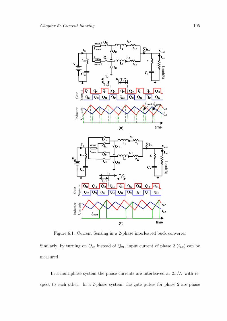
Chapter 6: Current Sharing 105
Load(R)
Load(R)
Gate
Signals
Gate
Signals
Inductor
Currents
Inductor
Currents
Figure 6.1: Current Sensing in a 2-phase interleaved buck converter
Similarly, by turning on Q23 instead of Q21, input current of phase 2 (iL2) can be
measured.
In a multiphase system the phase currents are interleaved at 2π/N with re-
spect to each other. In a 2-phase system, the gate pulses for phase 2 are phase

Chapter 6: Current Sharing 106
shifted by Ts/2 with respect to the gate pulses of phase 1, where Ts is the switching
period. In order to avoid simultaneous turning on of Q13 and Q23, an additional
phase shift of Ts/2 is used. That is, the switching of Q23 is delayed by 1.5 time
periods with respect to Q13, as shown in Fig. 6.1(b). Thus, in a 2-phase system
the switches Q13 and Q23 operate with a time period of 3Ts, or in other words with
a switching frequency of fs/3, where fs is the switching frequency of the converter.
This enables the current sensing of the two inductor currents in a time-interleaved
manner and avoids the simultaneous sensing of both the phases. The scheme can
be used with any current sensor. For example, a GMR sensor can be used to sense
the various inductor currents.
Although the proposed scheme is using higher number of switches, the in-
crease in cost due to switches is much less than the cost of having N-such sensors.
In addition, the switches can be integrated along with the control electronics re-
sulting in a power module. On the other hand, the GMR sensor still has to be
external to the ASIC.
In order to verify the functionality of the current sensing scheme, a two phase
interleaved converter was tested. The converter was operated in open loop and
the duty ratio of phase 1 was kept higher than that of phase 2, so as to result
in different phase currents. The current through the sensor was obtained using a
current probe. Fig. 6.2 shows the two inductor currents and the sensed current
as obtained using a current probe. A wire loop was used to sense the current
using current probe. This introduces an additional inductance while switching the

Chapter 6: Current Sharing 107
auxiliary switches. As a result the inductor current ripple in the two phases slightly
varies during their turn on.
ð
ñò
óò
ôò õö÷øùúûü ýøüüþöúÿ
úþ øÿþ
þöÿþ÷ ýøüüþöú
ð ð ÿ
Figure 6.2: Current sensing in a 2-phase system using single sensor
The current probe used above was to verify the functionality of the sensing
circuit. In actual circuit, the wire loop was removed and a Giant-Magneto Resistive
(GMR) effect based current sensor was used [76], [85]. It senses the magnetic field
associated with the current to be measured. The typical resistance offered by
commercially available GMR is around 5 kΩ. Thus when operating at 12V power
supply, it will result in a power consumption of 0.028W . This power consumed is
practically independent of the current to be measured.
6.2.2 Power Loss Analysis
For the circuit operation described above, (Q11, Q12) and (Q21, Q22) form
the conventional buck converter. The individual currents are sensed by switching
Q13 and Q23. This allows the individual phase currents to flow through the sensor.
Thus, for a given converter, either Q11 or Q13 will be switched at a time. Since Q11
and Q13 are identical and only one of them will be switched at a time, the scheme

Chapter 6: Current Sharing 108
does not result in additional losses.
6.2.3 Current Sharing
Fig. 6.3 shows the control architecture which is used for current sharing
among individual phases. For simplicity only two phases are shown. As shown
in the Fig. Cv is the voltage controller, Gi1d and Gi2d are the control to inductor
current transfer function for phase 1 and phase 2 respectively. Gvi is the total
inductor current to output voltage transfer function and C12 is the current sharing
controller used for balancing the individual currents. The proposed scheme is based
on difference in individual phase currents. The control strategy utilizes only voltage
controller. In a multi-phase converter, each phase takes the same duty ratio which
is obtained from voltage compensator. However under load dynamics, the phase
having the minimum inductance may carry the entire difference of the load current.
Moreover, in steady state, the phases may carry different currents due to variations
among individual phases. To mitigate this, the duty ratio is compensated for each
phase depending upon the current mismatch in the phase currents. This can be
explained by considering the inductor current dynamics which is given by
iL(k + 1) = iL(k) + (D(k).Vin(k)− Vout(k))Ts
L+ δiL (6.1)
where D(k) is the duty ratio, iL is the average inductor current and δiL accounts for
current due to un-modelled parameters resulting from mismatches and other non-
idealities. Current sharing of parallel phases is inherently guaranteed by properly
compensating for δiL for different phases. Thus the duty ratio of various phases

Chapter 6: Current Sharing 109
is compensated based on the circuit parameters. For this, only a voltage mode
control loop is required which gives the desired duty ratio D(k). Based on this
duty ratio, the duty ratio for various phases are adjusted so as to account for
unwanted disturbances.
d1(k) = D(k)−∆d12, d2(k) = D(k) + ∆d12, ... (6.2)
where ∆d12 is obtained based on the circuit parameters.
Figure 6.3: Two phase control architecture with duty ratio compensation for cur-rent sharing
Since the current sharing is based on difference in the individual average phase
currents, the current sharing does not get affected by the bandwidth of the outer
voltage loop.
In the scheme shown in Fig. 6.3, ∆d12 is computed based on the mismatch
in the average inductor currents e12 = iL1 − iL2. An increase (or decrease) in duty
ratio command of a phase results in increase (or decrease) in the phase current.

Chapter 6: Current Sharing 110
Thus, the duty ratios are compensated as,
d1(k) = D(k)− C12.e12 (6.3)
d2(k) = D(k) + C12.e12 (6.4)
where C12 is the current sharing (CS) controller.
For implementing this scheme, the difference in the individual currents is
used. The individual currents are sampled and stored according to the sensing
scheme described above. The duty ratios of individual phases are then updated
based on the current mismatch among the phases.
Figure 6.4: The proposed control architecture as applied to a 4-phase interleavedconverter
The current sharing scheme shown above is for two-phase converter. The

Chapter 6: Current Sharing 111
! " ##$ %&'()*
! +,-./ %+'()*
0123456
7123476
89: 8;:
8<: 8=:
>
?
@A
@B
@C@D
@EFGHI
0JKLMNOPQLPPRJNS456
>
?
@A @B
@C @D
@EFGHI
0JKLMNOPQLPPRJNS456
@A @B @C @D@EFGHI
>
?
0JKLMNOPQLPPRJNS456
Figure 6.5: Simulation results showing the performance of the scheme duringstartup transient (a) Output voltage and output current, (b) Distribution of loadcurrent among individual phases, (c) Mismatch between iL1, iL2 and iL3, iL4 and(d) Balanced inductor currents using proposed scheme
scheme is scalable in nature and can be extended to any number of paralleled
converters. Fig. 6.4 shows the scheme as applied to a 4-phase interleaved converter.
The duty ratio compensation is applied based on the difference between any two
phases. Compensating the duty ratios based on e12 = iL1 − iL2 and e34 = iL3 − iL4
will ensure these errors go to 0, however, there may still be current offsets between
iL1, iL2 and iL3, iL4.
This can be observed in Fig. 6.5 which shows the simulation results when the
proposed scheme is applied to a 4-phase interleaved converter. In order to have non-
identical phases, the inductance values were changed. The following parameters

Chapter 6: Current Sharing 112
are used for the simulation: Vin = 5V , Vref = 1.2V , Iout = 80A, L1 = 1.0µH,
L2 = 1.2µH, L3 = 1.3µH, L4 = 1.4µH and fs = 1MHz per phase. The system
was simulated using SIMPLORER Simulation System [73]. Fig. 6.5(a) shows the
output voltage and output current during the start-up transient and during the
steady-state while Fig. 6.5(b) shows the distribution of the load current among
the individual converters. It also shows the average of the output current of the
individual converters (iL(avg)). Fig. 6.5(c) shows the distribution of load current
when the duty ratios are compensated based on e12 = iL1− iL2 and e34 = iL3− iL4.
As seen from the simulation results, average output currents iL1 and iL2 match (i.e.
e12 = 0) and average output currents iL3 and iL4 match (i.e. e34 = 0), however, the
offsets are still to be compensated between (iL1, iL2) and (iL3, iL4). To compensate
the mismatch between these two pairs (iL1, iL2) and (iL3, iL4) an extra compensation
based on (iL(1,2) − iL(3,4)) is used. Using e23 = iL2 − iL3 and compensating for their
mismatch, the average output currents iL2 and iL3 can match (i.e. e23 = 0). This
can be verified from Fig. 6.5(d) which shows the distribution of load currents in
the four phases.
6.2.4 Stability Analysis
The scheme presented in Fig. 6.3 can be simplified as shown in Fig. 6.6. For
the sake of simplicity only one of the phase is shown. Under steady state operation,
the voltage error approaches 0 (Verr → 0). Hence a PI controller controlling the
voltage will give a constant duty ratio output (D). However, applying the same

Chapter 6: Current Sharing 113
TUV
TWX
YZV[
YWZ
\V ]^V_`abc
`baa
`def
`def
]^
X]^U
YZV[
gh
\V]^V
_
]^U TUV
ijk
ilk
mUV \UV
]^V
n^V
\UV
Figure 6.6: (a) Simplified control architecture based on duty ratio compensationfor achieving current sharing (b) Constant duty ratio D being updated based oncurrent mismatch
duty ratio to various phases results in different inductor currents. Here iL1 and iL2
are the average inductor current of phase 1 and 2 respectively and e12 = iL1 − iL2
is the measure of mismatch in the two phase currents. It is desired that iL2 should
follow iL1. Thus, the duty ratio of phase 2 is corrected as shown in Fig. 6.6(a).
For phase 2, assume that IL2 is the current due to steady state duty ratio (D)
and ∆iL2 is the change in current due to duty ratio correction (∆d12), as shown
in Fig. 6.6(b). Based on this, the transfer functions to describe the system can be
obtained as following:
iL2 =Gi2d
1 +Gi2dC12
D +Gi2dC12
1 +Gi2dC12
iL1 (6.5)
where C12 is the current sharing controller and Gi2d is the control to inductor
current transfer function for phase 2. Using this, the sensitivity (S) of closed-loop

Chapter 6: Current Sharing 114
transfer function to changes in the C12 can be evaluated as
SiL2
C12=
C12
iL2
∂iL2∂C12
=1
1 +Gi2dC12
(6.6)
Using (6.5) and (6.6), if the gain of loop transfer function is sufficiently high,
closed-loop performance can be made insensitive to changes in Gi2d and the phase
current iL2 follows iL1. But this may not result in a stable system. For maintaining
the stability of the system, the inductor current balancing control is analyzed to
determine the upper bound of controller gain. Using (6.1), the duty ratio is adjusted
such that the average currents are balanced. An increase in the duty ratio of
one converter results in increase in output current of that converter. The output
current of other converter(s) will decrease so as to maintain the same total current.
If e12 = iL1 − iL2 is the current mismatch, then for a damped system we have to
compensate for e12/2. Thus, for a stable system, we have the inequality as
|∆d12(k).Vin(k).Ts
L| ≤ |e12| (6.7)
Thus, the upper bound of the gain is obtained as
∆d12(k)
e12(k)≤ L
Vin · Ts
(6.8)
This upper bound ensures that the change in duty ratio (∆d12(k)) should not be
such that it changes the sign of the current error. Since the change in current
is proportional to the change in the duty ratio, thus a simple low-gain P-control
can be used to balance the inductor currents. Substituting the values (Vin = 5V ,
L = 1.2µH, Ts = 1µs), the upper bound of gain is obtained as max |C12| = 0.24.

Chapter 6: Current Sharing 115
o
po
qo
ro
qoo qso roo rso too tso soo sso
uvwx yzy|w~
uvwxw yzy|w~
y ¡¢¡£ y ¡¢£
o
to
o
o¤qs
o¤so
o¤¥s
p¤oo
p¤qs
qoo qso roo rso too tso soo sso
qo
¦§¨§ ©§ªª« ¬®
¦§¨§ ¯°±²³ ¬¯´µ®
¯´µ
¬²® ¬¶®
Figure 6.7: Simulation results showing the effect of increasing the gain of thecurrent sharing controller
The unstable operation resulting from high-gain of current sharing (CS) con-
troller can be observed in Fig. 6.7. It shows the simulation results when the
proposed scheme is applied to a 2-phase interleaved converter. In order to have
non-identical phases, the inductance values were changed. The following param-
eters were used for simulations: Vin = 5V , Vref = 1.2V , fs = 1MHz per phase,
L1 = 1.0µH, L2 = 1.2µH, Co = 2350µF and rc = 3mΩ. The system was subjected
to a load change of 10A to 40A. Fig. 6.7(a) shows the distribution of load current
among individual converters while Fig. 6.7(b) shows the output voltage and output
current during the load transient. The current sharing controller was enabled at
t = 350µs with |C12| = 0.03, resulting in sharing of average phase currents. How-
ever, it results in unstable operation when the gain of the current sharing controller
(C12) was increased to 0.3, which is greater than the limit given by (6.8).

Chapter 6: Current Sharing 116
6.2.5 Accuracy in current sharing
The accuracy in current sharing among various phases of a VRM is required
to be within 10% of the rated output current [5]. The proposed scheme uses
only a low gain P-control to achieve current sharing. Thus, due to the nature
of the current sharing controller, there may still be current mismatch among the
individual phases. The accuracy of current sharing can be obtained by evaluating
the difference in the various inductor currents under steady state. For example,
for a 2-phase system, the difference (|iL1 − iL2|) can be studied as the measure of
current sharing. The final value theorem is used to evaluate the measure of current
sharing between phase i carrying current iLi and phase j carrying a current of iLj.
∆Iij = lims→0
|iLi − iLj|, i 6= j (6.9)
As mentioned earlier, the current mismatch eij = iLi − iLj is processed by Cij to
obtain the change in the duty ratio. We analyze a simple P-controller which is used
as current sharing compensator. The upper limit on the gain of current sharing
controller was established as max |Cij| = 0.24. In a fixed point implementation, we
should have eij(k).Cij ≥ 1 for producing a minimal change in the duty ratio. Thus
the accuracy of current sharing is |eij(k)| ≤ 1|Cij |
. For example, in a typical digital
implementation, where an ADC with resolution of Vq is used to sample the sensed
current and the CS controller is Cij =18= 0.125, then the current mismatch is
|eij| ≤ 8.Vq (6.10)
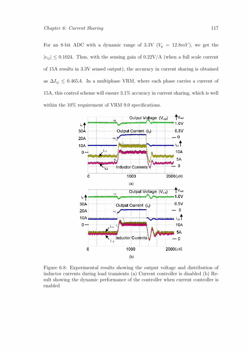
Chapter 6: Current Sharing 117
For an 8-bit ADC with a dynamic range of 3.3V (Vq = 12.8mV ), we get the
|eij| ≤ 0.1024. Thus, with the sensing gain of 0.22V/A (when a full scale current
of 15A results in 3.3V sensed output), the accuracy in current sharing is obtained
as ∆Iij ≤ 0.465A. In a multiphase VRM, where each phase carries a current of
15A, this control scheme will ensure 3.1% accuracy in current sharing, which is well
within the 10% requirement of VRM 9.0 specifications.
· ¸··· ¹···º »¼
·
¸·½
¹·½
¾·½
¿À
ÁÂÃ
ÄÅÆÇÈÉÊË ÌÇËËÍÅÉ»¿ÎÏ
¿ÎÐ
ÑÇÉÒÇÉ ÌÇËËÍÅÉ ºÓÔ¼
ÑÇÉÒÇÉ ÕÊÖÉ×ØÍ ºÕÔÙÚ¼
·ÛÜÕ
¸Û·Õ
ÝÀÞß
·
ܽ
¸·½
·
¿Îà
·
¸·½
¹·½
¾·½
ÄÅÆÇÈÉÊË ÌÇËËÍÅÉ» ·
ܽ
¸·½
¿ÎÏ
¿ÎÐ
¿Îà
¿À
ÑÇÉÒÇÉ ÌÇËËÍÅÉ ºÓÔ¼
ÑÇÉÒÇÉ ÕÊÖÉ×ØÍ ºÕÔÙÚ¼
·
·ÛÜÕ
¸Û·Õ
ÝÀÞß
· ¸··· ¹···º »¼
ÁáÃ
Figure 6.8: Experimental results showing the output voltage and distribution ofinductor currents during load transients (a) Current controller is disabled (b) Re-sult showing the dynamic performance of the controller when current controller isenabled

Chapter 6: Current Sharing 118
Q11 Q12
Q13
Q21 Q22
Q23
L1
L2
Wire loop to observe the
input current
Input
Output
GMR Sensor on the
bottom layer
Q13
Q23
Figure 6.9: Experimental prototype of the two phase converter used to demonstratethe proposed current sensing scheme.
6.3 Experimental Results
The performance of the proposed method for current sensing was tested on a
buck converter prototype with the following parameters: Vin = 5V , Vref = 1.25V ,
L = 1.2µH, Co = 3200µF (tantalum), fsw = 1MHz and N=2 phases. Fig. 6.9
shows the prototype which was built in the laboratory. A wire loop used to verify
the functionality of the sensing scheme. After the functionality was verified, the
loop was replaced with a copper trace such that the current flows along the top
layer. The GMR sensor AAL002 was used for current sensing with its supply

Chapter 6: Current Sharing 119
voltage at 12V. The sensor was placed on the bottom layer of the PCB board and
current was made to flow through the top layer. Since average current control is
desired, the average value of the inductor current can be obtained by sensing the
current in the middle of the switch-on and switch-off intervals. A digital controller
was used to verify the performance of the system. In the prototype, the ADC had 8-
bit resolution (NADC = 8) and DPWM had 6-bit of hardware resolution. Thus 3-bit
digital dither was introduced to increase the effective resolution of DPWM module
to 6+3=9 bits (NDPWM = 9). The controller was implemented on a Spartan-3
FPGA board from Xilinx.
Fig. 6.8(a) shows the response of the system when the converter was subjected
to load transients with a step-up change in the phase current from 5A per phase
to 10A and vice versa. The load transients were generated by switching the load
resistance. In order to see the current mismatch among the two phases, the current
controller is disabled and is working with a voltage controller only. The reference
voltage is set as 1V. Fig. 6.8(a) shows the distribution of the inductor currents in a
voltage mode controlled multiphase converter. In order to test the performance of
the current sensing and sharing method using a single current sensor, the current
controller is enabled. Fig. 6.8(b) shows the response of the system when the
converter was subjected to similar load transients. It shows good sharing of the
inductor currents after compensating the duty ratios of the two phases.
These results were to test the performance of the current sensor under load dy-
namics. In practice the VRM output requires adaptive voltage positioning (AVP).

Chapter 6: Current Sharing 120
In adaptive voltage positioning, the output voltage of the VRM is adapted to
changes in the load. This causes the output voltage to droop with the load.
Adaptive voltage positioning was implemented by changing the reference volt-
age in accordance with the load current. Reference voltage is defined as vref =
Vref − io ·Rdroop, where Vref is the nominal reference voltage at no load conditions,
io is the load current and Rdroop is the droop resistance obtained from the load
line. Fig. 6.10 shows the dynamic response of the controller with adaptive voltage
positioning for a step change in load current from 10A to 25A and vice versa.
â ãâââ äâââå æç
èéêëéê ìéííîïê åðñç
òííóí åîôõöð÷ôøð÷õç
ùúûüýþÿ
â
ãâ
ïéêóí ìéííîïêæ
â
ãâ
ãâ
ãâ
äâ
â
ý
èéêëéê óêî åñç
ýþû
ýþú
â
Figure 6.10: Experimental results showing the dynamic performance of the con-troller with adaptive voltage positioning for a step load change
6.4 Summary
Voltage mode-control can be used to obtain high bandwidth of the closed
loop systems, however it does not ensure current distribution. Current mode con-
trol can be used but it requires individual current loops and hence it will require
N -sensors for N -paralleled converters. Reducing the number of sensors impose

Chapter 6: Current Sharing 121
an extra computational overhead on the current sharing controller. Thus, a cur-
rent sharing scheme is presented, which uses single sensor to sense the individual
currents. The scheme is independent of the number of converters in the paralleled
system. A GMR based current sensor is used which is practically lossless. The pro-
posed sharing scheme can be implemented easily on a digital platform and provides
various functionalities of a voltage regulating module. The proposed scheme is in-
dependent of the number of converters in the paralleled system. The functionality
of the current sensing method is experimentally verified on a 2-phase interleaved
buck converter, both under steady state and under load transients.
Current sensing is used for providing various functionalities in DC-DC con-
verters. It may be used for over-current protection or for achieving load sharing
among paralleled converters. It may also be used for implementing current-mode
control for improving the transient response of the closed loop system. The current
mode control will improve the transient response of the system, but the response
gets limited by the slew rate of the inductor current. For a buck converter with
large conversion ratio (Vin >> Vout), the step-down transients last longer than the
step-up transients. To this end, the next chapter develops a new circuit topology,
which helps in improving the step-down transient response in such a buck converter.

122
Chapter 7
Improving the Step-DownTransient Response
7.1 Introduction
During a step-down load transient, a large amount of charge is absorbed by
the output capacitor in a very short time. This results in an overshoot in the
output voltage. Similarly, during a step-up load transient, capacitor removes the
required charge so as to meet the load current demand. This results in a voltage
undershoot if the capacitor cannot provide the required current sufficiently fast.
In a buck converter, the inductor voltage determines the slew rates during step-up
(ρu) and during step-down load transients (ρd), as illustrated using Fig. 7.1. Due
to different slew rates, an asymmetrical transient response occurs during increase
and decrease in load.
The slew rates depend upon the voltage across the inductor and are given as:
ρu =diLdt
|up =Vin − Vout
L(7.1)

Chapter 7: Step-Down Topology 123
Load (A)
outL indI V -V=
dt L
OutputVoltage(V)
Load (A)
OutputVoltage(V)
outLdI V=-
dt L
Figure 7.1: Charging and discharging of the output capacitor during sudden changein load current
ρd =diLdt
|down = −Vout
L(7.2)
For a given change in load current (∆Io), the time taken by the inductor current
to attain the new value will be Tup =∆Ioρu
and Tdown = ∆Ioρd
respectively. The step-
down transient will last longer than the step-up transient if it satisfies the following
condition,
Tdown > Tup (7.3)
∆Ioρd
>∆Ioρu
(7.4)
∆Io · LVout
>∆Io · L
Vin − Vout
(7.5)
This can be simplified as
Vin > 2 · Vout (7.6)
Since (7.6) is normally the case for a low conversion ratio buck converter, the rate
of increase of inductor current is much higher as compared to the rate of decrease of

Chapter 7: Step-Down Topology 124
inductor current. Thus, for a given change in load current, the charge supplied by
output capacitor is smaller than the charge absorbed by the capacitor. This results
in larger voltage overshoot as compared to the voltage undershoot. The following
example evaluates the condition which results in larger overshoot as compared to
the undershoot.
The undershoot of output voltage for a ∆Io step-up change in load current
can be obtained as (see Appendix A)
∆vundershoot =1
2(∆I2oρu.Co
+ ρu.r2c .Co),
∆Ioρu
> rc.Co (7.7)
∆vundershoot = ∆Io.rc,∆Ioρu
≤ rc.Co (7.8)
where rc is the effective series resistance of the output capacitor, Co is the output
capacitance and ρu is the slew rate of the inductor current. Similarly, the voltage
overshoot for the same step-down change in load current can be obtained as
∆vovershoot =1
2(∆I2oρd.Co
+ ρ2.r2c .Co),
∆Ioρd
> rc.Co (7.9)
∆vovershoot = ∆Io.rc,∆Ioρd
≤ rc.Co (7.10)
where ρd is the rate of change of inductor current.
Assuming ∆Ioρu
> rc.Co and ∆Ioρd
> rc.Co, the voltage overshoot will be higher
than the voltage undershoot, if the following condition is satisfied:
∆vovershoot −∆vundershoot > 0 (7.11)
1
2(∆I2oρd.Co
+ ρd.r2c .Co)−
1
2(∆I2oρu.Co
+ ρu.r2c .Co) > 0 (7.12)

Chapter 7: Step-Down Topology 125
The above expression can be simplified as
1
2(ρu − ρd)[
∆I2oρu.ρd.Co
− r2c .Co] > 0 (7.13)
Using (7.6), the slew rates have the relation ρu > ρd. Thus for (7.13) to be true,
∆Io > rc.Co.√ρu.ρd (7.14)
Using (7.1) and (7.2), this can be simplified as
∆Io >rc.Co
L.√(Vin − Vout).(Vout) (7.15)
Similarly, in another case when ∆Ioρu
< rc.Co and∆Ioρd
> rc.Co, the difference between
voltage overshoot and undershoot is
∆vovershoot −∆vundershoot > 0 (7.16)
1
2(∆I2oρd.Co
+ ρd.r2c .Co)− (∆Io.rc) > 0 (7.17)
(∆Io − ρd.rc.Co)2 > 0 (7.18)
which is always true. Using the relation ∆Ioρ2
> rc.Co, it can be established that for
an asymmetrical transient response, the load change should satisfy
∆Io > ρd.rc.Co (7.19)
As a design example, the following parameters are used Vin = 5V , L =
1.2µH, Co = 408µF (tantalum) and rc = 1mΩ. Using the above analysis, it
can be deduced that ∆Io > 0.34A at an output voltage of 1V will produce an
asymmetrical transient response. This can also be seen from Fig. 7.2 which shows

Chapter 7: Step-Down Topology 126
! " #$%
&'()'(*+,(-./0*1234
5 6 7 8 9 : ; < = 5>
>?9
5?>
5?9
6?>
6?9
7?>
7?9
8?>
8?9
9?>
@ABCDEFAAG H @IJKCDEFAAG
@ABCDEFAAG L @IJKCDEFAAG
@ABCDEFAAG M @IJKCDEFAAG
Figure 7.2: Region showing the comparison of voltage overshoot and undershootfor load transients of different magnitudes
the comparison of voltage overshoot and voltage undershoot for load transients of
different magnitudes at various output voltages.
If the change in load current satisfies (7.15) or (7.19) depending upon the
time constant of the output capacitance (rc.Co), it will result in an asymmetrical
transient response with a higher voltage overshoot than the undershoot. One way
to reduce the overshoot is to increase the size of the output capacitance. This is
undesirable as it increases the size of the voltage regulating module. Another way
to reduce the voltage overshoot is to decrease the inductor current faster. However,
the rate of change of inductor current depends on the value of circuit inductance
and the voltage across the inductance |diL/dt| = |vL/L|. The magnitude of the
slew rate can be increased by increasing the magnitude of the voltage across the
inductor or by reducing the inductance value.
In the past various methods have been proposed to improve the transient re-

Chapter 7: Step-Down Topology 127
sponse of the system. These methods rely on one or more of the following methods:
• Increasing the size of the output capacitor to reduce the voltage overshoot
• Reducing the circuit inductance so as to increase the rate of change of inductor
current [10],[54],[55]
• Using feed-forward techniques to shape the load characteristics [56] - [58]
• Using non-linear control action during the load transients [59]- [64]
• Including an additional clamping circuit to limit the voltage overshoot [65],
[66].
The above mentioned methods, either try to reduce the inductance value
or incorporate non-linear control action during the load transients. Reducing the
inductance results in higher inductor current ripple and hence results in higher
losses. On the other hand, a non-linear control action would saturate the controller
faster. It would change the speed of the response to disturbance but the maximum
slew rate gets limited by the inductance value and the voltage across it. Thus,
there are limitations in these past approaches and they can not be directly applied
to meet the challenging requirements of high currents at high slew rates and tight
voltage regulation.
In a buck converter, when the high side MOSFET is turned off, the voltage
across the inductor is vL = −Vout, which limits the slew rate of inductor current
during a step-down load transient. In the proposed scheme, the slew rate during

Chapter 7: Step-Down Topology 128
such a transient is increased by increasing the magnitude of voltage across the
inductors. The voltage across the inductor is changed by applying negative input
voltage across it. Fig. 7.3 shows the proposed topology and the three modes of
operation.
In the proposed scheme, the voltage across the inductor is changed during
transient load. During transients, the fast rate of change of inductor current is
achieved by applying a negative voltage across the inductor. When the load tran-
sient is over and the fast rate of change is no longer required, the voltage across
the inductor is reduced and eventually restored to its original value. In doing so,
the steady state ripple is kept to a minimum while providing fast dynamics during
transients.
The proposed scheme, by increasing the slew rate of the inductor current in
DC-to-DC converters, achieves the following:
1. Reduced voltage overshoots during load transients in DC to DC converters.
2. Faster settling times of output voltage during transients.
3. Smaller output capacitor as it can provides reduced voltage undershoots.
4. Maintains a lower ripple current in the inductor of DC to DC converters.
In short, the proposed scheme is capable of providing fast dynamic performance
during transients without significantly deteriorating the steady state behavior.

Chapter 7: Step-Down Topology 129
7.2 Proposed Scheme: Working Principle
A sudden decrease in the load current will cause an overshoot in the output
voltage. To mitigate this overshoot effect, the current absorbed by the output
capacitor of the DC to DC converter during such a transient has to be decreased.
This is achieved by changing the slew rate of the inductor current. For a constant
value of inductance, the slew rate depends on the voltage across the inductor. It
is proposed to increase this rate during the load transients. The increased rate has
to be sustained as long as the load is changing and is restored to its original value
once the transient is over.
Fig. 7.3 shows the proposed topology. It is derived from the conventional
buck converter topology. Switch Q1 and D1 comprises of the conventional buck
converter. In the proposed scheme, Q2 and D2 are added. During the steady state
operation, switch Q2 is kept on. As a result, it works as a normal buck converter,
with Q1 as its high-side switch and diode D1 as the free-wheeling diode. However,
during step-down load transients, Q2 is disabled and the current is forced through
D2. It may be noted that during step-down transients, the circuit disconnects the
input voltage ground from the output voltage ground. Thus, the proposed scheme
requires a floating power supply. The main power source for the VRM on mother
board is 12V, which is obtained from a Switched Mode Power Supply (SMPS).
The SMPS is essentially a full bridge rectifier followed by a forward converter. The
output of such a transformer based power converter is floating which can be used

Chapter 7: Step-Down Topology 130
Q1
Q2
D2
D1
LiL
Cin
LO
AD
Vo
Io
Vin
iin
Co
rc
iC
Q1
Q2
D2
D1
L
iL
Cin
LO
AD
Vo
Io
Vin
iin
Co
rc
iC
Mode 1: Q1 and Q2 are ON
Q2
D2
D1
L
iL
Cin
LO
AD
Vo
Io
Vin
Co
rc
iC
Mode 2: Q1 is OFF and Q2 is ON
D2
D1
L
iL
Cin
LO
AD
Vo
Io
Vin
Co
rc
iC
Mode 3: Q1 and Q2 are OFF
1
Figure 7.3: (a) The proposed converter for improving the step-down load transients.(b) Equivalent circuit during its three modes of operation.
as the input for the proposed scheme.
The operation of the circuit can be divided into three modes. The equivalent
circuit during these modes are given in Fig. 7.3(b)
Mode 1: Q1 and Q2 are on and the inductor current is increasing. The
voltage across the inductor is vL = Vin − Vout.
Mode 2: Q1 is turned off, while Q2 is still on. The inductor current flows
through the free-wheeling diode D1. As a result, the current in the inductor is

Chapter 7: Step-Down Topology 131
decreasing. The voltage across the inductor is vL = −Vout.
Mode 3: Q1 and Q2 are turned off. The inductor current flows through
D2, D1 and through the input capacitance. The voltage across the inductor is
vL = −Vin − Vout. As a result, the inductor current decreases at a much higher
rate.
It may be noted that Mode 1 and Mode 2 are similar to the conventional
buck converter. In addition to these, Mode 3 is introduced during step-down load
transients so as to improve the dynamic response of the system. In the conventional
buck converter, the inductor current will decrease with a rate of −Vout/L while in
the proposed scheme, it can decrease at a rate of (−Vin−Vout)/L. Thus for a given
change in load current (∆Io), the time taken for the inductor current to fall to the
new level can be obtained as:
T |conv =∆Io · LVout
(7.20)
T |proposed =∆Io · L
Vout + Vin
(7.21)
This gives us the improvement over the conventional scheme as
T |proposedT |conv
=Vout
Vin + Vout
(7.22)
Assume that the output voltage does not change appreciably and is held constant
during such a transient. Thus, for Vin = 5V and Vout = 1V , it will provide a
6x improvement in the fall time. In this analysis, we have assumed ideal diodes
and ideal switches. A more accurate analysis can be obtained by considering the
voltage drop across these devices.

Chapter 7: Step-Down Topology 132
7.2.1 Switching Algorithm
Since it is intended to increase the slew rate of inductor current, it needs
to have a switching algorithm which decides to operate the converter in Mode 3,
as described above. The working of the error based control algorithm is explained
using the current loop only. Later the idea can be extended to obtain the algorithm
based on the output voltage.
NO
PQRS
TUVWXYZ[Y\[] ^[]_
`Ya] b c d
ef
g]hiZ`]j ^[]_
`Ya] b klm d
n
opqrstuvwrvvxptyz
|NO
| c~
Z]` ^[]_
`Ya] b ~ d
Figure 7.4: Difference in the slew rates - required and available
Current Mode Control: Suppose there is a sudden change in reference
current at time t = 0. The available slew rate due to circuit inductance is ρ1 A/s
while the required rate is ρref A/s (ρref > ρ1), as shown in Fig. 7.4. A higher
rate of ρ2 A/s is also available by operating the converter in Mode 3, as described
above. In a current mode controlled converter, current error is processed. By
the end of one sampling instance, the current error in the normal case will be
e = (ρref − ρ1).Ts where Ts is the sampling period. The idea here is to minimize
the error by increasing the available slew rate ρ1 to ρ2. By using ρ2, the error will
be e = (ρref − ρ2).Ts. Thus it will reduce the error by ∆e = (ρ2 − ρ1).Ts. This can

Chapter 7: Step-Down Topology 133
be used as the current threshold for the proposed design.
eth = (ρ2 − ρ1).Ts (7.23)
If the error is higher than the eth, the converter is switched to Mode 3 operation,
otherwise it continues to operate with its normal conditions. For example, in a
buck converter with Vin = 5V , Vout = 1V and having an inductance of 1µH, a slew
rate of 1A/µs is available during the step down operation. Using the proposed
scheme, will correspondingly achieve 6A/µs. Thus, if the error after a duration Ts
is higher than eth, that is e > (6− 1).Ts, then the converter is operated in Mode 3,
else it continues in its normal operation.
The proposed scheme was first tested on a buck converter having only the
current loop. The converter parameters are Vin = 5V , Co = 408µF , L = 1.2µH,
fs = 1MHz. The system was subjected to a 10A step change in reference current
(Iref ) from 15A to 5A. For a given controller, the performance was compared with
the normal case. Same controller was used in both the cases, except that an
additional Mode 3 was used as per the proposed scheme. An over current signal
based on the current error was used to switch to Mode 3 operation. It is seen from
the simulation results in Fig. 7.5, the fall time and the settling time are improved
by increasing the magnitude of voltage across the inductor during transients.
Voltage Mode Control: A switching algorithm based on output voltage can
also be formulated, which increases the slew rate during the step-down operation,
so as to keep the voltage overshoot within the permissible limits.

Chapter 7: Step-Down Topology 134
¡ ¢£¡¡ ¤¥
¦§¨¨©ª «¬¨©
®©¯§ª°¨
¦§¨¨©ª
¡ ¢£¡¡ ¤¥
¦§¨¨©ª «¬¨©
®©¯§ª°¨ ¦§¨¨©ª
±²³¥´µ ´¶¡²·· ¥¸ ¹¤º£¶¥²¡ »¼½ ±²³¥´µ ´¶¡²·· ¥¸ ¹¤º£¶¥²¡ »¼½
¾¿ ¾¿
À·
Figure 7.5: Simulation result showing the performance of the proposed schemeduring a step change in current reference. (a) Conventional Scheme (b) Proposedscheme using the same converter parameters as the conventional scheme
Consider a power converter having its output voltage regulated at Vref . Dur-
ing a step-down load transient, a large amount of charge is added to the capacitor
in a very short time. This results in an overshoot in the output voltage. Two
factors contribute to the voltage drop; voltage drop due to resistance dVR = ic.rc,
and voltage drop due to discharge of the capacitor dVQ = ∆Q(t)/Co. Here, Co is
the output capacitor and rc is the effective series resistance of the capacitor.
A hysteresis based control algorithm is also established which is used to switch
the mode of operation, so as to obtain an improved transient response. In such
a method, two threshold voltages are defined above the nominal output voltage
(VH and VL), with VH > VL. While the output voltage remains below the upper
threshold (VH) converter is working with the normal conditions. If the step-up load
transient is observed, the output voltage will start to increase. Once the output
voltage increases above the upper threshold (VH), the Mode 3 is enabled and the
converter starts to respond with increased slew rate. The normal operation is re-

Chapter 7: Step-Down Topology 135
stored, once the output voltage falls below the lower threshold voltage (VL). The
thresholds can be chosen smaller than the limits imposed by the output voltage reg-
ulation specifications under load dynamics. This will ensure the voltage overshoot
remains within the permissible limits. It can be verified by using the following
example, in which the higher slew rate is switched after the output voltage has
increased to a certain level.
In this analysis, ρ1 is the available slew rate and the higher slew rate (ρ2) is
applied at a time instance t1 during the load transient, as shown in Fig. 7.6. At
any any arbitrary instance t (t > t1), the capacitor current can be evaluated as
ic(t) = ∆Io − ρ1t1 − ρ2(t− t1) (7.24)
The charge absorbed by the capacitor during the interval (0− t1) is given by
∆Q1(t) =1
2t1(2∆Io − ρ1t1) (7.25)
where ∆Io is the change in the load current. The charge absorbed by the capacitor
during the interval (t1 − t) is given by
∆Q2(t) = ∆Io(t− t1) + (ρ2 − ρ1)t1t− (ρ2 − ρ1)t21 ++
1
2ρ2(t
21 − t2) (7.26)
Thus, the total charge absorbed by the output capacitor in time (0− t) is ∆Q1 +
∆Q2, which is obtained as
∆Q(t) = ∆Iot+ (ρ2 − ρ1)t1t−1
2(ρ2 − ρ1)t
21 −
1
2ρ2t
2 (7.27)

Chapter 7: Step-Down Topology 136
ÁÂÃÄÂÃÅÆÇÃÈÉÊËÅÌ
ÍÆÈÎËÏÌ Ð
ÑÒÓÒÔ
Figure 7.6: Typical waveforms during step change in the load. The input voltageis switched after time t1
The voltage overshoot during such a case can be expressed as,
∆v(t) =∆Q(t)
Co
+ ic(t).rc
∆v(t) =∆IoCo
t+ (ρ2 − ρ1)(t1t
Co
− 1
2
t21Co
)− ρ2t2
2Co
+ (∆Io − ρ1t1 − ρ2(t− t1))rc(7.28)
The overshoot will be maximum, when ∆v(t)dt
= 0. The time instance can be
obtained as
t =1
ρ2(∆Io + (ρ2 − ρ1)t1 − ρ2rcCo) (7.29)
Substituting this t in (7.28), overshoot is obtained as
∆vOS,new =1
2Coρ2[∆I2o + C2
oρ22r
2c + 2∆Io(ρ2 − ρ1)t1 + ρ1(ρ1 − ρ2)t
21] (7.30)
The normal case voltage overshoot can be obtained by substituting ρ1 = ρ2 and
t1 = 0 in (7.30) as
∆vOS,old =1
2(∆I2oρ1.Co
+ ρ1.r2c .Co) (7.31)
For the proposed scheme to be effective, the voltage overshoot should decrease by

Chapter 7: Step-Down Topology 137
increasing the slew rate,
∆vOS,old −∆vOS,new > 0 (7.32)
ρ2 − ρ12Coρ1ρ2
[−C2or
2cρ1ρ2 + (∆Io − ρ1t1)
2] > 0 (7.33)
Since ρ2 > ρ1, the above expression is simplified as
[−C2or
2cρ1ρ2 + (∆Io − ρ1t1)
2] > 0 (7.34)
This is a quadratic equation in t1. This gives us the time instance before which
the higher slew rate should be switched on so as to reduce the voltage overshoot.
t1 <∆Ioρ1
± Corc
√ρ2ρ1
(7.35)
The value with the plus sign corresponds to the time instance after the transient
is over. Thus the value with the negative sign is retained .
t1 <∆Ioρ1
− Corc
√ρ2ρ1
(7.36)
Under the limiting case, the maximum value of time interval is obtained when t1
approaches its upper limit. The voltage change at this instance is obtained by
substituting
t1 =∆Ioρ1
− Corc
√ρ2ρ1
(7.37)
in (7.28). The voltage change is obtained as
∆v(t)|t=t1 =∆I2o2Coρ1
+ Cor2c
√ρ1ρ2 − Cor
2cρ2 (7.38)
Thus, for the given load change (∆Io), if the Mode 3 is switched before the voltage
rises by the value given in (7.38), the overshoot can be reduced. This sets the limit

Chapter 7: Step-Down Topology 138
on the threshold values (VH) for the hysteresis controller.
VH ≤ Vref +∆v(t)|t=t1 (7.39)
VH ≤ Vref + (∆I2o2Coρ1
+ Cor2c
√ρ1ρ2 − Cor
2cρ2) (7.40)
The threshold voltage is chosen such that it satisfies the limit imposed in (7.40).
If the output voltage rises above the threshold voltage (VH), the converter will
switch to Mode 3, so as to increase the slew rate and hence to reduce the voltage
overshoot during the load transient. This also corresponds to a time instance
defined by (7.37). Applying the negative inductor voltage within time t1, after the
load transient occurs, will reduce the voltage overshoot. The input can be restored
to its normal value once the output voltage decreases below the lower threshold
voltage (VL). The lower threshold is chosen close to the reference voltage such that
VH > VL.
The above analysis was done for a buck converter having a voltage loop
only. However, a cascaded voltage and current control loop is recommended for
improved dynamic response. This is because, the main component of the solution
that brings about the improvement is based on increase in inductor current slew
rate, hence an inner current loop is advantageous. The foregoing analysis based
on voltage controlled converters is also applicable for converters operating with
cascaded control loops. In order to verify the this, a buck converter with the
following parameters was simulated: Vin = 5V , Co = 408µF , rc = 1mΩ, L =
1.2µH, fs = 1MHz. The system was subjected to a 10A step change in load
current (Io) from 15A to 5A. The load transients were generated by switching the

Chapter 7: Step-Down Topology 139
load resistance. The converter was operated with cascaded control loops, where
the reference voltage was kept constant as Vref = 1V . For the given converter
parameters, the upper limit on the voltage overshoot given in (7.38) is obtained as
145.7mV. A voltage overshoot of 40mV was used to enable the switching algorithm
(VH = 1.040V ), which is within the limit obtained in (7.40). For a given controller,
the performance was compared with the normal case. Same controller was used
in both the cases, except that an additional error based switching algorithm was
used to apply a higher magnitude of voltage across the inductor. It is seen from
the simulation results in Fig. 7.7, the voltage overshoot and the settling time are
improved by increasing the magnitude of the voltage across the inductor during
the step-down transients. The increased input voltage helps in increasing the slew
rate of the inductor current and hence results in faster transient response.
ÕÖ×ØÙÚÛ ÙÜÝÖÞÞ ØßÛ àáâãÜØÖÝ äåæç
èéêëìíîï ðëïïñéí òèóô
õëíöëí ðëïïñéí òè÷ô
õëíöëí øîùíúûñ òø÷üýô
õþñï øîùíúûñ òõøô
ÿ
ÿ
ø÷üý
þó
ø
ÿ
ÿ
õëíöëí øîùíúûñ òø÷üýô
èéêëìíîï ðëïïñéí òèóô
õëíöëí ðëïïñéí òè÷ô
õþñï øîùíúûñ òõøô
ÕÖ×ØÙÚÛ ÙÜÝÖÞÞ ØßÛ àáâãÜØÖÝ äåæç
ø÷üý
þó
ø
Figure 7.7: Simulation result showing the performance of the proposed schemeduring a step change in load current. (a) Conventional Scheme (b) Proposed schemeusing the same converter parameters as the conventional scheme
The above mentioned analysis was based on a buck converter so as to improve
its transient response. These arguments can be extended to improve the step-down
transient response of other topologies as well. It is concluded that it is possible

Chapter 7: Step-Down Topology 140
to increase the step-down slew rate of the inductor current without reducing the
inductance. The increased slew rate results in faster transient response. This will
also reduce the size of the output capacitor.
7.2.2 Output Capacitor Design
During a step-down load transient, the output capacitor absorbs the excess
of inductor current. This results in voltage overshoot. The voltage overshoot for
a given load transient is obtained in (7.31). The relation (7.31) is used to find
the required capacitance for a given voltage overshoot. In a conventional buck
converter, for a 10A change in load current and a voltage overshoot less than
100mV , it would require an output capacitance of Co = 601.5µF . By using the
proposed scheme, the voltage overshoot is obtained in (7.30) which also includes
the delay in activation of Mode 3. In our system, the maximum delay between the
occurrence of load transient and the activation of Mode 3 is around 1µs. Hence the
worst case value of capacitance to maintain the given voltage overshoot during such
a transient is 180.7µF which amounts to 69.9% reduction in output capacitance.
7.2.3 Slew rate determines the fall time
The fall time of inductor current during a step-down transient can be de-
creased by having a high bandwidth and by having high slew rates. However at
high bandwidth, the linear PI controllers get saturated and produce a duty ratio of
either 0 or 1. Under such condition, the fall time is determined only by the slew rate

Chapter 7: Step-Down Topology 141
in the circuit. The slew rate is determined by diL/dt = vL/L. For step-down tran-
sients, the slew rate in conventional circuit is limited to diL/dt = −Vout/L. On the
other hand, in the proposed circuit the slew rate becomes diL/dt = −(Vin+Vout)/L.
For example, in a buck converter with Vin = 5V , L = 1.2µH and an output volt-
age of 1V , the minimum fall time achievable for a 10A change in inductor current
will be 12µs. As opposed to that in the proposed circuit, the voltage across the
inductor is −(Vin + Vout), thus for Vout = 1V , the fall time can be reduced to 2µs.
!
"
#
$"
$#
%"
%#
&"
&#
$"'
$"#()*+,*-./ 0123
4567 89:;<=>?@=ABCD
EFGHGIJK
LM7JNJ
4567 89:;=ABC:;$=
OGP8JP65GPQR
LM7JNJ
OGP6FGRRJF
LQ6SFQ6JI
T5PJQF
UQPVJ
$W XYZ
[QPK45K67
T5N56
%\ XYZ
Figure 7.8: Reducing the fall time by increasing the slew rate of the inductorcurrent
Thus, an increase in bandwidth can reduce fall time only in linear range
where the controllers are not saturated. However, increasing the slew rate brings
about a reduction in fall time under the maximum limits of circuit operation. In
addition, high slew rates will produce faster fall times for the same bandwidth in
the proposed method. This can be seen from Fig. 7.8. It shows the fall time
for a buck converter having the following parameters: Vin = 5V , L = 1.2µH,
Co = 408µF , rc = 1mΩ and Vout = 1V . The controllers are designed for a given

Chapter 7: Step-Down Topology 142
bandwidth and the fall time of the closed loop system is obtained for a 10A change
in the reference current, which is greater than the condition established in (7.15).
It is seen that in conventional scheme, increasing the bandwidth reduces the fall
time in the linear range. However, beyond 18kHz the fall time is determined by the
slew rate in the circuit. Whereas in the proposed scheme, the fall time is reduced
by increasing the slew rate.
7.2.4 Power Loss Analysis
In a practical circuit, synchronous rectifiers will be used instead of the diodes,
as shown in Fig. 7.9. For the circuit operation described earlier, the inductor
current will flow through switch Q2. Since Q2 will be on during normal operation,
the conduction loss in switch Q2 can be obtained as [23]
PQ2 = [I2o +∆I2
12].Ron,Q2 (7.41)
where Io is the output current, ∆I is the inductor current ripple, Ron,Q2 is the
on-state resistance of switch Q2.
Q1
Q2
D2
D1
LiL
LO
AD
Vo
Io
iin
Vin
Co
rc
iC
(a)
Q1
Q2
S2
S1
L
iL
LO
AD
Vo
Io
iin
Vin
Co
rc
iC
(b)
Figure 7.9: (a) The proposed scheme using diodes. (b) The diodes are replaced bysynchronous rectifiers
For this analysis, the data of the commercially available MOSFETs can be

Chapter 7: Step-Down Topology 143
used which have the specifications suitable for such a low-voltage high-current ap-
plication. Considering our specifications and the ratings, Infineon 25V n-channel
MOSFET IPB03N03LA seems appropriate. Hence the on-resistance of the semi-
conductor switches is taken as 2.2mΩ. An interleaved buck converter is commonly
used for high current VRMs, where the load current is shared by the paralleled
modules. An inductor current of around 10A to 20A is common in an individual
buck converter in such a topology. For a 5V-1V/10A buck converter having the
inductor current ripple of 1A, the conduction loss incurred in the switch Q2 will be
0.220W, which is 2.2% of the output power. Thus, in the proposed scheme, a 6x
improvement in the response time is achieved at the expense of additional loss of
0.220W.
]^_`
abcd e fgdhijkbl
mnhhdlj
mbljhboodh
pqra
sabcd tuvw
xyz| ~
mnhhdlj
dlbh
bojid
dlbh
niljkdh
bojid
mbljhboodh
af
phkdh
b afk
q bihc
^_`
niljkdh
^_` ^_`
ds¡w¢d£
¤
¥
¦^_`
Figure 7.10: Schematic of digital controller design using FPGA

Chapter 7: Step-Down Topology 144
7.2.5 Implementation of Proposed Scheme
A digital controller was used to obtain the desired performance of the system.
The digital controller performs various tasks including the voltage and current
control, digital pulse width modulation and implementing the switching algorithm.
The block schematic of a digital controller is shown in Fig. 7.10. The control
algorithm requires the output voltage (Vout) and the inductor current (IL). The
sampled voltage is processed using the voltage controller to obtain the current
reference (Iref ). The current error is obtained as (e = Iref − IL). The threshold
current error (eth) for switching to Mode 3 is obtained in (7.23). It depends on
the slew rates ρ1 and ρ2, which are fixed for the given converter parameters. If the
current error exceeds the threshold, the converter is switched to Mode 3 to increase
the slew rate, else it continues in its normal operation.The scheme shown above
is based on the current error. However, the scheme based on voltage error is also
possible as described earlier.
7.3 Experimental Results
The performance of the proposed method was tested on a buck converter
prototype with the following parameters: Vin = 5V , Vref = 1V , L = 1.2µH,
Co = 220µF + 4× 47µF (tantalum), rc = 1mΩ, fs = 1MHz. Fig. 7.11 shows the
experimental prototype which was used to demonstrate the proposed scheme. The
full load current of the converter is limited to 16A. Such currents are typical in the

Chapter 7: Step-Down Topology 145
Q1
S1
L
Input
Output
Q2S2
Gate
Drivers
Figure 7.11: Experimental prototype of the buck converter used to demonstratethe proposed scheme.
individual converters of an interleaved buck converter topology, which is commonly
used in VRMs. Since the main objective was to see the improvement in the slew rate
of inductor current, it was demonstrated on a 1V/16A buck converter. A digital
controller was used to verify the performance of the proposed scheme. The inductor
current and the output voltage was sampled using an ADC. The ADC had 8-bit
resolution (NADC = 8) and DPWM had 6-bit of hardware resolution. Thus 3-bit
digital dither was introduced to increase the effective resolution of DPWM module
to 6+3=9 bits (NDPWM = 9). The controller was implemented on a Spartan-3
FPGA board from Xilinx operating at a clock frequency of 50MHz.
The dynamic response of inner current loop was studied to see the effect of
step change in the reference current. Fig. 7.12 shows the response of the system
when the converter was subjected to step change in the reference current from 16A

Chapter 7: Step-Down Topology 146
Figure 7.12: Experimental result showing the performance of the system with astep change in reference current. (a),(b) Conventional converter (c),(d) Proposedbuck converter
to 3A. Fig. 7.12 (a),(b) shows the response of current loop in a conventional buck
converter, while Fig. 7.12 (c),(d) shows the response of the proposed scheme. Same
PI controller was used in both these cases, except that an over current signal was
used in Fig. 7.12 (c),(d) to apply a negative voltage across the inductor.
In conventional scheme, assuming the output voltage constant, the rate of
change of inductor current will be −Vout/L, whereas in the proposed scheme it will
be (−Vin − Vout)/L. For Vin = 5V , Vref = 1V , L = 1.2µH, one would expect
6x improvement in the response time. As seen from the experimental results, 7x
improvement is obtained by using the proposed scheme. The fall time in conven-
tional case is 21µs, which is reduced to less than 3µs with the proposed scheme.

Chapter 7: Step-Down Topology 147
Since this result is based on inner current loop alone, the output voltage decreases
following a decrease in inductor current. This results in the slew rate to change
during the step down transient resulting in a larger fall times than predicted.
The system was also tested for load transients with a step-down change from
12A-2.5A. Fig. 7.13 shows the dynamic response of the converter. Cascaded
voltage and current controllers were used to regulate the output voltage with its
reference voltage set at 1V. It shows the change in the output voltage during load
transient. The load transients were generated by switching the load resistance and
the voltage undershoot (∆Vout) is obtained by using the AC coupling in a passive
probe. Fig. 7.13 (a) is the conventional scheme, while Fig. 7.13 (b) is using the
proposed scheme. Same controllers were used in both these cases, except that an
additional over voltage signal was used in Fig. 7.13 (b) to apply negative voltage
across the inductor. The overshoot in conventional scheme is 226mV which is
reduced to 161mV using the proposed scheme. The transient time is also reduced
from 235µs to 144µs.
7.4 Summary
For a low conversion buck converter, a step-down load transient is more crit-
ical than the step-up load transient. During a step-down load transient, the maxi-
mum rate of decrease of inductor current depends upon the circuit inductance and
the output voltage. As a result, the step-down transients last longer than then
step-up transient. To this end, a new buck topology is presented which provides

Chapter 7: Step-Down Topology 148
Figure 7.13: Experimental result showing the output voltage and inductor currentduring load transients in a buck converter with cascaded control loops (a) Responseof the Conventional buck converter (b) Response of the proposed buck converter
improved step-down transient. From the experimental and simulation results, it is
concluded that the proposed scheme is effective in improving the step-down tran-
sient response. Using the proposed scheme, it is possible to increase the slew rate
of the inductor current, without having to reduce the inductance.
The proposed scheme improves the step-down transient response, thus reduc-
ing the voltage overshoots. In practical microprocessor applications, the voltage
overshoots have long term reliability concerns whereas the voltage undershoots di-

Chapter 7: Step-Down Topology 149
rectly impacts the overall performance of the system. Thus it is also important to
reduce the voltage undershoots during a step-up load transient. The next chapter
proposes such a scheme.

150
Chapter 8
Improving the Step-Up TransientResponse
8.1 Introduction
During a step-up change in load current, the charge supplied by output ca-
pacitor is more than the charge absorbed by the capacitor. This results in an
undershoot of the output voltage. One way to reduce the undershoot is to increase
the size of the output capacitance. This is undesirable as it increases the size of the
voltage regulating module. Another way to reduce the voltage undershoot is to in-
crease the inductor current faster. However, the rate of change of inductor current
depends on the value of circuit inductance and the voltage across the inductance
|diL/dt| = |vL/L|. The magnitude of the slew rate can be increased by increasing
the magnitude of the voltage across the inductor or by reducing the inductance
value.
In the past various methods have been proposed to improve the transient re-

Chapter 8: Step-Up Topology 151
sponse of the system. These methods rely on one or more of the following methods:
• Increasing the size of the output capacitor to reduce the voltage overshoot
• Reducing the circuit inductance so as to increase the rate of change of inductor
current [10],[54],[55]
• Using feed-forward techniques to shape the load characteristics [56] - [58]
• Using non-linear control action during the load transients [59]- [64]
• Including an additional clamping circuit to limit the voltage overshoot [65],
[66].
The above mentioned methods, either try to reduce the inductance value or
incorporate non-linear control action during the load transients. However, the max-
imum possible slew rate is limited by the inductance value and the voltage across
it. On the other hand, a non-linear control action would saturate the controller
faster. It would change the speed of the response to disturbance and the best
they can achieve is the maximum slew rate. They can’t exceed the available slew
rate. Secondly, the transient response will be governed by the instance at which
the non-linear control action is applied and the duration it is applied. Thus, there
are drawbacks in the previous schemes which limit their applications. These past
approaches are unable to address the generic problem of high slew rates and meet
the challenging requirements of high currents at high slew rates and tight voltage
regulation.

Chapter 8: Step-Up Topology 152
§¨§©
ª©
ª¨
ª«
¬®§¯°±²³´²³
µ¯¶¯·¯¸¹
¬º»¼
½¾¿ÀÁÂÃÄ ÅÆÇÆÁ¿ÀÈÉ
Å¿ÉÁÊ¿À
ËÌÍÎÏ ÏÐ ÏÑÒÓÐÌÔÒÕÏÒÕ
§¨§©
ª©
ª¨
ª«
¨
§¯°±²³´²³
µ¯¶¯·¯¸¹
¬º»¼
ËÌÍÎÏ ÏÐ ÏÑÒÓÐÌÔÒÕÏÒÕ
¬® ¨¬®
¬Ö׬®Ø¬ÙÚÛ ¬Öר¬®Ø¬ÙÚÛ
½¾¿ÀÁÂÃÄ ÅÆÇÆÁ¿ÀÈÉ
Å¿ÉÁÊ¿ÀÜÝÞ ÜßÞ
àáâ àáâã
ää
ãàáâ
ä
ãàáâ
ã
ä
Figure 8.1: Working principle of the proposed scheme. The voltage across theinductor is changed by altering the input voltage
8.2 Proposed Scheme
The inductor current slew rate is given as diL/dt = vL/L, where vL is the
voltage across the inductor and L is the inductance. In a buck converter, when
the high side MOSFET is turned on, the voltage across the inductor is vL =
Vin − Vout. Thus the slew rate depends on the circuit inductance, the input and
the output voltage. Fig. 8.1 shows the working principle of the proposed scheme,
which increases the slew rate by changing the voltage across the inductors. The
voltage across the inductor can be changed by altering the input voltage. This is
realized using a multilevel voltage generator, such as a switched capacitor circuit
for obtaining different voltage levels. In Fig. 8.1(a) the voltage across the inductor
is vL = Vin − Vout, whereas in Fig. 8.1(b) it is increased to vL = 2Vin − Vout. The
Fig. shows only two levels of input voltage, it can be extended to obtain higher
voltage levels.
Switched-capacitor based circuits have been used for voltage conversion [86]

Chapter 8: Step-Up Topology 153
- [89]. In this scheme, a switched-capacitor circuit is used to increase the input
voltage to the converter. Increasing the input voltage increases the slew rate of
inductor current without having to reduce the inductance value. The capacitor
network provides the desired voltage level based on a switching algorithm, which
uses knowledge of the circuit behavior. Moreover, since it has to work with a closed
loop control, it has to have the correct logic interfaces with the outer loop. Thus,
the proposed scheme includes the following: 1) an energy storage element, 2) a
switching system, 3) an error based switching algorithm and 4) a feedback loop.
In the proposed scheme, the voltage across the inductor is changed during
transient load. During transients, the fast rate of change of inductor current is
achieved by increasing the voltage across the inductor. When the load transient is
over and the fast rate of change is no longer required, the voltage across the inductor
is changed to its original value. In doing so, the steady state ripple is kept to a
minimum while providing fast dynamics during transients. This is realized using
a switched capacitor circuit, which can generate multiples of an input voltage by
appropriately controlling the switches associated with the circuit. The switches
are ON only for a small duration. During startup, the switches are turned ON to
charge the switched capacitor network. During transients, selective switches are
turned ON again to increase the input voltage as required. By doing so, the slew
rate of inductor current is increased which provides faster dynamic response to a
load transient.
The proposed scheme achieves higher slew rates without having to reduce

Chapter 8: Step-Up Topology 154
Table 8.1: Slew rate comparison for different levels of input voltages in a buckconverter
Inductance L = 1µH
Scheme Used Normal scheme Proposed Scheme
Number of Voltage Levels n=1 n=2 n=5
Slew Rate Achieved 4A/µs 9A/µs 24A/µs
Equivalent Inductance∗ 1 µH 0.44 µH 0.166 µH
Inductance L = 100nH
Scheme Used Normal scheme Proposed Scheme
Number of Voltage Levels n=1 n=2 n=5
Slew Rate Achieved 40A/µs 90A/µs 240A/µs
Equivalent Inductance∗ 100 nH 44.4 nH 16.6 nH
∗ Inductance required to obtain the slew rate using the normal scheme with constant input
voltage
the inductance value. Table 8.1 shows the achievable slew rates for different levels
of input voltage. Nominal input voltage is Vin = 5V and the output voltage is
assumed to be Vout = 1V . It is assumed, the input voltage can be increased
by integral multiples as nVin. In the conventional scheme, the input voltage is
constant (n = 1). The table shows the slew rates for two different cases, one
where 2 input levels are available (n = 2) and second where 5 input levels are
available (n = 5). The table 8.1 gives the slew rates for a single buck converter.
The slew rates can be increased further by paralleling operation, as in the case of
an interleaved buck converter. It is concluded that for a single buck converter, it
is possible to increase the slew rate of the inductor current without reducing the
inductance. For example, with 100nH inductance a slew rate of 40A/µs can be

Chapter 8: Step-Up Topology 155
achieved. By using 5Vin, a slew rate of 240A/µs can be achieved, which would have
required an inductance of 16.6nH in the normal case. Such small inductors are
difficult to fabricate. The high slew rates mentioned above are common in voltage
regulator modules. For meeting such high slew rates, inductance value has to be
reduced in nH range. However, smaller inductance will result in higher steady
state ripple resulting in higher losses in the circuit. Thus, the proposed scheme can
be used in such applications allowing us to increase the slew rate without reducing
the inductance any further. The increased slew rate will result in faster transient
response. This will also reduce the size of the output capacitor.
The proposed scheme, by increasing the slew rate of the inductor current in
DC-to-DC converters achieves the following:
1. Reduced voltage undershoots during load transients in DC to DC converters.
2. Faster settling times of output voltage during transients.
3. Smaller output capacitor as it can provides reduced voltage undershoots.
4. Maintains a lower ripple current in the inductor of DC to DC converters.
5. It can be applied to any switched mode power converter for increasing the
slew rate of inductor current.
In short, the proposed scheme is capable of providing fast dynamic perfor-
mance during transients without significantly deteriorating the steady state behav-
ior.

Chapter 8: Step-Up Topology 156
8.2.1 Working Principle
A sudden increase in the load current will cause an undershoot in the output
voltage. To mitigate this undershoot effect, the average current supplied to the
output capacitor of the DC to DC converter has to be increased to match the
current supplied by the output capacitor to the load. This is achieved by changing
the slew rate of the inductor current. For a constant value of inductance, the slew
rate depends on the voltage across the inductor. The slew rate is increased by
increasing the voltage across the inductor. The increased rate has to be sustained
as long as the load is changing. Hence, to minimize the undershoot, the control
scheme needs to sense the drop in output voltage. If the drop in the output voltage
is above the permissible limit, the control algorithm is activated to change the
voltage across the inductor, resulting in an appropriate slew rate that can reduce
the time for the drop in the output voltage.
Since it is intended to increase the slew rate of inductor current, so the working
of the error based control algorithm is explained using the current loop only. Later
the idea can be extended to obtain the algorithm based on the output voltage.
Case I: Converters having current control loop: In DC-to-DC convert-
ers having an inner current loop and an outer voltage loop, the inductor current IL
is sensed for control purposes. IL is compared with the desired reference current,
Iref and the current error is compensated. In the proposed scheme, an error based
switching algorithm is used to decide the multiple of input voltage that needs to be

Chapter 8: Step-Up Topology 157
applied so as to minimize the current error. The scheme is shown in Fig. 8.2 which
obtains the required input voltage (nVin) to be applied to the converter. This can
be explained with the following example.
Vin
IrefSwitching
Algorithm
e(t)
IL
Input to the
converter
Vout
Co
Q1
Q2
Io
Load
rcIL
L rL
Buck Converter
nVin
Required
Input Voltage
Multi-Level
Generator
IL
Time
IrefAvailable Slew
rate ( 1 )
Ts
Required Slew
rate ( 2 )
e
InductorCurrent(A)
dIL
dt1
2
Increasing Vin
(a)
(b)
Figure 8.2: Difference in the slew rates - required and available. The slew rate isincreased by increasing the input voltage.
Suppose there is a sudden change in reference current at time t = 0. The
available slew rate due to circuit inductance is ρ1 A/s while the required rate is
ρ2 A/s (ρ2 > ρ1), as shown in Fig. 8.2. By the end of one sampling instance, the
current error will be e = (ρ2 − ρ1).Ts where Ts is the sampling period. The idea
here is to minimize the error by increasing the available slew rate ρ1. The rate

Chapter 8: Step-Up Topology 158
ρ1 is determined by the voltage across the inductance, where ρ1 = (Vin − Vout)/L.
The rate ρ1 can thus be increased by increasing the input voltage. It is assumed
that the input voltage can be increased by integral multiples of Vin. The required
input voltage (n.Vin) can be calculated such that the error e as shown in (8.1) is
minimized.
e = (ρ2 −nVin − Vo
L)Ts (8.1)
For example, in a buck converter with Vin = 5V , Vout = 1V and having an
inductance of 1µH, a slew rate of 4A/µs is available. Doubling the input voltage
to 2Vin achieves a slew rate of 9A/µs and tripling the input voltage to 3Vin will
correspondingly achieve 14A/µs. Thus, if the error after a duration Ts is within
the range (9− 4).Ts < e < (14− 4).Ts, then the input voltage is increased to 2Vin.
If the error is more than (14− 4)Ts, the input voltage is increased to 3Vin.
In general, it is desirous to find the input voltage such that the error is
minimized. In other words, n is calculated such that the error lies within the
range:
(nVin − Vout
L− Vin − Vout
L)Ts < e < (
(n+ 1)Vin − Vout
L− Vin − Vout
L)Ts (8.2)
Or equivalently,
(n− 1)Vin
LTs < e <
(n)Vin
LTs (8.3)
This gives the required input voltage n.Vin which is to be obtained using
the multi-level voltage generator. Once the required input voltage n.Vin is known,
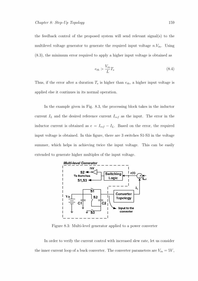
Chapter 8: Step-Up Topology 159
the feedback control of the proposed system will send relevant signal(s) to the
multilevel voltage generator to generate the required input voltage n.Vin. Using
(8.3), the minimum error required to apply a higher input voltage is obtained as
eth >Vin
LTs (8.4)
Thus, if the error after a duration Ts is higher than eth, a higher input voltage is
applied else it continues in its normal operation.
In the example given in Fig. 8.3, the processing block takes in the inductor
current IL and the desired reference current Iref as the input. The error in the
inductor current is obtained as e = Iref − IL. Based on the error, the required
input voltage is obtained. In this figure, there are 3 switches S1-S3 in the voltage
summer, which helps in achieving twice the input voltage. This can be easily
extended to generate higher multiples of the input voltage.
åæåç
èç
èæ
èé
êëìåíîïðñòðñ
óíôíõíö÷
øùúû
èüýòþÿýîö
íöýþ
ø
! " "
#$
èç%èé
èæ
Figure 8.3: Multi-level generator applied to a power converter
In order to verify the current control with increased slew rate, let us consider
the inner current loop of a buck converter. The converter parameters are Vin = 5V ,

Chapter 8: Step-Up Topology 160
Co = 408µF , L = 1µH and fs = 1MHz. The system was subjected to a 10A
step change in reference current (Iref ) from 5A to 15A. Two different cases were
simulated, one where only 2 input levels are available and second where 5 input
levels are available. For a given controller, the performance was compared with
the normal case where input voltage is kept constant. Same controller was used in
all the three cases, except that an additional error based switching algorithm was
used to switch the input voltage. It is seen from the simulation results in Fig. 8.4,
the rise time and the settling time are improved by increasing the input voltage
during transients.
&
'&
(
)&
)(
'(& '*& '+& ',&
-./0123450446.2
789: ; <=
&
'&
(
)&
)(
'(& '*& '+&
-./0123450446.2
789:; <=
>?@AB CDEBFG: ;CHI='CHI
(CHI
JAKK:?B L:M:K:?N:
ODK9FE JF<:
P8BQ 'CHI
P8BQ (CHI
>?@AB CDEBFG: ;CHI='CHI
(CHI
P8BQ 'CHI
P8BQ (CHI
ODK9FE JF<:
JAKK:?B L:M:K:?N:
;F= ;R=
Figure 8.4: Simulation result showing the performance of the proposed schemeduring a step change in current reference. (a) Closed loop bandwidth of 50kHz (b)Closed loop bandwidth of 100kHz
Case II: Switching Algorithm based on Hysteresis Control: A switch-
ing algorithm based on output voltage can be formulated, which increases the input
to the converter, thus increasing the slew rate of inductor current and keeps the
voltage undershoot within the permissible limits.
Consider a power converter having its output voltage regulated at Vref . Dur-

Chapter 8: Step-Up Topology 161
ing a step-up load transient, a large amount of charge is removed from the capacitor
in a very short time. This results in a drop in the output voltage. Two factors
contribute to the voltage drop; voltage drop due to resistance dVR = ic.rc, and
voltage drop due to discharge of the capacitor dVQ = ∆Q(t)/Co. Here, Co is the
output capacitor and rc is the effective series resistance of the capacitor, as shown
in Fig. 8.5.
Co
Load
rc
L
IoIL
iC
Io
Charge to be supplied by
the output capacitor
time
IL ρ = =1
-in outL V VdIdt L
0 t
iC
Available Slew rate ( )
T
ρ1Io
Figure 8.5: Discharging of output capacitor during sudden load change
A hysteresis based control algorithm is established which is used to switch
the desired input voltage, so as to obtain an improved transient response. In such a
method, two threshold voltages are defined below the nominal output voltage (VLH
and VLL), with VLH > VLL. While the output voltage remains above the lower
threshold (VLL) converter is working with the nominal input voltage. If the step-
up load transient is observed, the output voltage will start to decrease. Once the
output voltage falls below the lower threshold (VLL), the input voltage is increased
and the converter starts to respond with increased slew rate, recharging the output
capacitors. The input voltage is restored, once the output voltage increases above
the upper threshold voltage (VLH). The thresholds can be chosen smaller than the

Chapter 8: Step-Up Topology 162
limits imposed by the output voltage regulation specifications under load dynamics.
This will ensure the voltage drop remains within the permissible limits. It can be
verified by using the following example, in which the input voltage is switched after
the output voltage has dropped to a certain level.
STUVTUWXYUZ[\]W^
_XZ`]a^
bcdefghi
bjklkm
Figure 8.6: Typical waveforms during step change in the load. The input voltageis switched after time t1
In this analysis, ρ1 is the available slew rate and the higher slew rate (ρ2) is
applied at a time instance t1 during the load transient, as shown in Fig. 8.6. At
any any arbitrary instance t (t > t1), the capacitor current can be evaluated as
ic(t) = ∆Io − ρ1t1 − ρ2(t− t1) (8.5)
The charge supplied by the capacitor during the interval (0− t1) is given by
∆Q1(t) =1
2t1(2∆Io − ρ1t1) (8.6)
where ∆Io is the change in the load current. The charge supplied by the capacitor
during the interval (t1 − t) is given by
∆Q2(t) = ∆Io(t− t1) + (ρ2 − ρ1)t1t− (ρ2 − ρ1)t21 +
1
2ρ2(t
21 − t2) (8.7)

Chapter 8: Step-Up Topology 163
Thus, the total charge supplied by the output capacitor in time (0−t) is ∆Q1+∆Q2,
which is obtained as
∆Q(t) = ∆Iot+ (ρ2 − ρ1)t1t−1
2(ρ2 − ρ1)t
21 −
1
2ρ2t
2 (8.8)
The voltage drop during such a case can be expressed as,
∆v(t) =∆Q(t)
Co
+ ic(t).rc
∆v(t) =∆IoCo
t+ (ρ2 − ρ1)(t1t
Co
− 1
2
t21Co
)− ρ2t2
2Co
+ (∆Io − ρ1t1 − ρ2(t− t1))rc (8.9)
The undershoot will be maximum, when ∆v(t)dt
= 0. The time instance can be
obtained as
t =1
ρ2(∆Io + (ρ2 − ρ1)t1 − ρ2rcCo) (8.10)
Substituting this t in (8.9), undershoot is obtained as
∆vdip,new =1
2Coρ2[∆I2o + C2
oρ22r
2c + 2∆Io(ρ2 − ρ1)t1 + ρ1(ρ1 − ρ2)t
21] (8.11)
The normal case voltage undershoot can be obtained by substituting ρ1 = ρ2 and
t1 = 0 in (8.11) as
∆vdip,old =1
2(∆I2oρ1.Co
+ ρ1.r2c .Co) (8.12)
For the proposed scheme to be effective, the voltage undershoot should decrease
by increasing the slew rate,
∆vdip,old −∆vdip,new > 0 (8.13)
ρ2 − ρ12Coρ1ρ2
[−C2or
2cρ1ρ2 + (∆Io − ρ1t1)
2] > 0 (8.14)

Chapter 8: Step-Up Topology 164
Since ρ2 > ρ1, the above expression is simplified as
[−C2or
2cρ1ρ2 + (∆Io − ρ1t1)
2] > 0 (8.15)
This is a quadratic equation in t1. This gives us the time instance before which
the higher slew rate should be switched on so as to reduce the voltage undershoot.
t1 <∆Ioρ1
± Corc
√ρ2ρ1
(8.16)
The value with the plus sign corresponds to the time instance after the transient
is over. Thus the value with the negative sign is retained.
t1 <∆Ioρ1
− Corc
√ρ2ρ1
(8.17)
Under the limiting case, the maximum value of time interval is obtained when
t1 approaches its upper limit. The voltage drop at this instance is obtained by
substituting
t1 =∆Ioρ1
− Corc
√ρ2ρ1
(8.18)
in (8.9). The voltage drop is obtained as
∆v(t)|t=t1 =∆I2o2Coρ1
+ Cor2c
√ρ1ρ2 − Cor
2cρ2 (8.19)
Thus, for the given load change (∆Io), if the input voltage is increased before the
voltage drops to the value given by (8.19), the undershoot can be reduced. This
sets the limit on the threshold values (VLL) for the hysteresis controller.
VLL ≥ Vref −∆v(t)|t=t1 (8.20)
VLL ≥ Vref − (∆I2o2Coρ1
+ Cor2c
√ρ1ρ2 − Cor
2cρ2) (8.21)

Chapter 8: Step-Up Topology 165
If the output voltage drops below the threshold voltage (VLL), the controller will
switch the input voltage to a higher level, so as to reduce the voltage undershoot
during the load transient. This also corresponds to a time instance defined by
(8.18). Switching the input voltage to a higher level within time t1, after the load
transient occurs, will reduce the voltage undershoot. The input can be restored
to its normal value once the output voltage increases above the upper threshold
voltage (VLH). The upper threshold is chosen close to the reference voltage such
that VLH > VLL.
The above analysis was done for a buck converter having a voltage loop only.
However, a cascaded voltage and current control loop is recommended for improved
dynamic response. This is because the main component of the solution that brings
about the improvement is based on increase in inductor current slew rate, hence an
inner current loop is advantageous. The foregoing analysis based on voltage con-
trolled converters is also applicable for converters operating with cascaded control
loops. In order to verify the this, a buck converter with the following parameters
was simulated: Vin = 5V , Co = 408µF , rc = 3mΩ, L = 1.2µH, fsw = 1MHz. The
system was subjected to a 10A step change in load current (Io) from 5A to 15A.
The load transients were generated by switching the load resistance. The reference
voltage was kept constant as Vref = 1V . For the given converter parameters, the
upper limit on the voltage drop given in (8.19) is obtained as 27.6mV. A voltage
drop of 25mV was used to enable the switching algorithm (VLL = 0.975V ). For
a given controller, the performance was compared with the normal case where in-

Chapter 8: Step-Up Topology 166
put voltage is kept constant. Two cases were simulated - one a converter having
2 levels of input voltage and second a converter having 5 levels of input voltage.
Same controller was used in all the three cases, except that an additional error
based switching algorithm was used to switch the input voltage. It is seen from the
simulation results in Fig. 8.7(a), the voltage undershoot and the settling time are
improved by increasing the input voltage during transients. This is also seen from
Fig. 8.7(b) which shows the inductor current in the three cases. The increased
input voltage helps in increasing the slew rate of the inductor current and hence
results in faster transient response.
n
op
p
qn
qp
on
rsn pon ptn
uvwxy z|y~zoz
pz
ns
n
qn
xywxy ¡x¢¢vy
£¤¥¦¤¥§¤¨©ª¥«¬
p
qn
qp
rsn pon ptn
xywxy z|y~
®
Figure 8.7: Simulation result showing the performance of the proposed schemeduring a step change in the load current. (i) Normal case where input voltage iskept constant, (ii) Converter having 2 levels of input voltage and (iii) Converterhaving 5 levels of input voltage.
The simulation results shown above were to test the performance of the pro-
posed scheme. It is concluded that it is possible to increase the slew rate of the
inductor current without reducing the inductance. The increased slew rate results
in faster transient response. This will also reduce the size of the output capacitor.
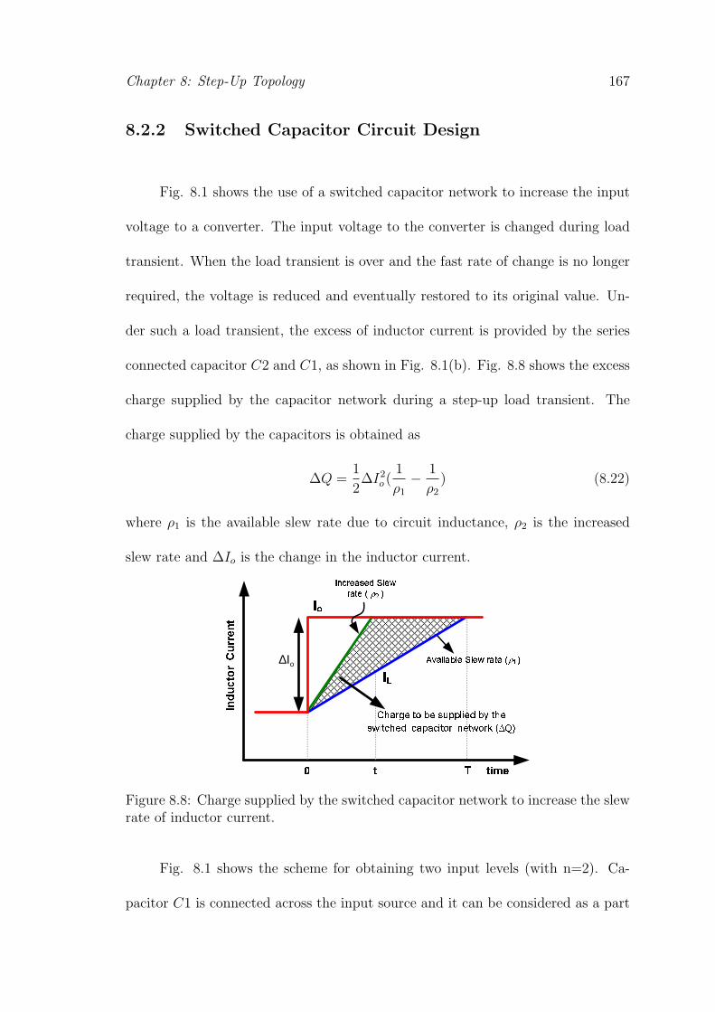
Chapter 8: Step-Up Topology 167
8.2.2 Switched Capacitor Circuit Design
Fig. 8.1 shows the use of a switched capacitor network to increase the input
voltage to a converter. The input voltage to the converter is changed during load
transient. When the load transient is over and the fast rate of change is no longer
required, the voltage is reduced and eventually restored to its original value. Un-
der such a load transient, the excess of inductor current is provided by the series
connected capacitor C2 and C1, as shown in Fig. 8.1(b). Fig. 8.8 shows the excess
charge supplied by the capacitor network during a step-up load transient. The
charge supplied by the capacitors is obtained as
∆Q =1
2∆I2o (
1
ρ1− 1
ρ2) (8.22)
where ρ1 is the available slew rate due to circuit inductance, ρ2 is the increased
slew rate and ∆Io is the change in the inductor current.
¯°
±²³´µ¶ ·¸ ¹¶ º»¼¼½¾¶¿ ¹À ·²¶
ºÁ¾·Â²¶¿ ³¼³Â¾·¸´ ö·Á¸´Ä Å ÆÇ
ÈÉÊË
¯Ì
Í È
ÎÏÐÑÒÐÓÒÔ ÕÒÔÖ ×ÐØÔ Ù Ú∆ oI
Û
ÜÝÞ×ÔÐßÔà ÕÒÔÖ×ÐØÔ Ù á Ú
â
Figure 8.8: Charge supplied by the switched capacitor network to increase the slewrate of inductor current.
Fig. 8.1 shows the scheme for obtaining two input levels (with n=2). Ca-
pacitor C1 is connected across the input source and it can be considered as a part

Chapter 8: Step-Up Topology 168
of the input capacitor. As a result the voltage across capacitor C1 will be Vin.
The excess of charge delivered will cause the voltage across C2 to decrease. In this
work, the voltage drop across the capacitor is designed to be less than ±1% of its
steady state value.
∆vC2 =∆Q
C2=
1
2
∆I2oC2
(1
ρ1− 1
ρ2) ≤ 1%Vin (8.23)
Thus, the required capacitance value of C2 can be calculated as
C2 ≥ 1
2
∆I2o0.01Vin
(1
ρ1− 1
ρ2) (8.24)
For the above mentioned parameters, Vin = 5V , Vout = 1V , L = 1µH, n = 2,
the slew rates are ρ1 = 4A/µs and ρ2 = 9A/µs. For a 10A change in load
current, the capacitance is obtained C2 ≥ 138.9µF . If 5% variation is allowed in
the capacitance voltage, the required capacitance will be C2 ≥ 27.7µF .
The voltage drop for a given load transient is obtained in (8.12). The relation
(8.12) is used to find the required capacitance for a given voltage undershoot. In
a buck converter with its input voltage fixed, for a 10A change in load current
and a voltage undershoot less than 30mV , it would require an output capacitance
of Co = 857.9µF . By using the proposed scheme where 2 · Vin is available, it
would require an output capacitance of Co = 381.3µF for obtaining the same
voltage drop. But in order to implement this, C2 of 138.8µF is added, as obtained
in eq. (8.24). Thus, in the proposed scheme the total capacitance required is
381.3µF + 138.8µF = 520.1µF , which is 39.6% less than the capacitance required
in the normal case (Co = 857.9µF ). If 5% variation is allowed in the capacitance
voltage, the required capacitance will 52.3% less than the normal case.

Chapter 8: Step-Up Topology 169
The above mentioned algorithm formulations were designed for a buck con-
verter so as to improve its transient response. These arguments can be extended
to other topologies as well.
8.2.3 Slew rate determines the rise time
The rise time of inductor current during a step-up transient can be decreased
by having a high bandwidth and by having high slew rates. However at high
bandwidth, the linear PI controllers get saturated and produce a duty ratio of
either 0 or 1. Under such condition, the rise time is determined only by the slew
rate in the circuit. The slew rate is determined by diL/dt = vL/L. For step-
up transients, the slew rate in a conventional buck converter circuit is limited to
diL/dt = (Vin − Vout)/L. On the other hand, in the proposed circuit the slew rate
becomes diL/dt = (nVin−Vout)/L. For example, in a buck converter with Vin = 5V ,
L = 1.0µH and an output voltage of 1.2V , the minimum rise time achievable for a
10A change in inductor current will be 2.6µs. As opposed to that in the proposed
circuit, the voltage across the inductor is (nVin−Vout), thus for n = 2, the rise time
can be reduced to 1.2µs and for n = 5, it can be reduced to 0.42µs.
Thus, an increase in bandwidth can reduce the rise time only in linear range
where the controllers are not saturated. However, increasing the slew rate brings
about a reduction in rise time under the maximum limits of circuit operation. In
addition, high slew rates will produce faster rise times for the same bandwidth in
the proposed method. This can be seen from Fig. 8.9. It shows the rise time for

Chapter 8: Step-Up Topology 170
ãäå
ãäæ
ãäç
èéêëìíëîï ðñòó
äôæ
ãôä
ãôæ
õôä
õôæ
öôä
öôæ
åôä
åôæ
æôä
÷øùúûøüúýùþ
äôä
ÿ
õ
æ
ããä
ãçä õæä
Figure 8.9: Reducing the rise time by increasing the slew rate of the inductorcurrent
a buck converter with the given parameters. The controllers are designed for a
given bandwidth and the rise time of the closed loop system is obtained for a 10A
change in the reference current. It is seen that in conventional scheme, increasing
the bandwidth reduces the rise time in the linear range. However, beyond 110kHz
the rise time is determined by the slew rate in the circuit. Whereas in the proposed
scheme, the rise time is reduced by increasing the slew rate.
8.2.4 Power Loss Analysis
The simplified schematic of the proposed scheme is shown in Fig. 8.10. It
shows a buck converter using a switching algorithm based on current error (e(t)).
The converter has a switched capacitor network at its input which can generate
Vin and 2Vin. Under the normal operating conditions, switch S1 and S3 will be
on, such that the input to the converter is Vin. As a result the input current will
flow through the switch S1. The current flowing through S1 will be same as that

Chapter 8: Step-Up Topology 171
Load
Figure 8.10: Block schematic of the proposed scheme showing a buck converter anda switched capacitor network at its input
in the control FET (Q1) of the buck converter. Thus, the conduction loss in the
switch S1 can be obtained as [23]
PS1 = [I2o +∆I2
12].Ron,S1.D (8.25)
where Io is the output current, ∆I is the inductor current ripple, Ron,S1 is the on-
state resistance of switch S1 and D is the duty ratio of Q1. Only during transients,
S2 will be turned on and S1,S3 will be switched off, such that the input to the
converter is 2Vin. Since this will be done only during the load transients and will
last only for a few micro-seconds, the switching losses in the switched capacitor
network can be neglected.
For this analysis, the data of the commercially available MOSFETs is used
which have the specifications suitable for such a low-voltage high-current appli-
cation. Considering our specifications and the ratings, Infineon 25V n-channel
MOSFET IPB03N03LA seems appropriate. Hence the on-resistance of the semi-

Chapter 8: Step-Up Topology 172
conductor switches is taken as 2.2mΩ. The switching frequency of the converter
is 1MHz. For 1V/20A buck converter having an input voltage of 5V and inductor
current ripple of 1A, the conduction loss and switching loss in the Control FET are
0.216W and 0.802W respectively. Similarly for the Synchronous FET these loses
are 0.864W and 0.797W respectively. In the proposed scheme, the conduction losses
incurred in the switch S1 will be 0.216W, which is 0.90% of the output power. Al-
though it results in increased conduction loss, the increase does not significantly
affect the overall efficiency.
Furthermore, the on-resistance (Rds,ON) of a MOSFET depends upon its
breakdown voltage [90], [91] as:
Rds,ON ∝ V 2∼2.5br (8.26)
As the proposed scheme intends to increase the input voltage during load transients,
this will require MOSFETs of higher breakdown voltage to be used. Even in
practice, the MOSFETs are usually chosen having breakdown voltages around 2-
2.5 times the input voltage. This is to take into account the ringing produced
during device turn-on and turn-off. In our application, where the input voltage
is Vin = 5V , n-channel MOSFETs with breakdown voltage of 25V were chosen.
n-channel Power MOSFETs with breakdown voltage less than 20V are difficult to
find. Since 25V is well within the range, our prototype did not result in increased
losses due to use of over rated devices.

Chapter 8: Step-Up Topology 173
8.2.5 Implementation of Proposed Scheme
A digital controller was used to obtain the desired performance of the system.
The digital controller performs various tasks including the voltage and current
control, digital pulse width modulation (DPWM) and implementing the switching
algorithm. The block schematic of a digital controller is shown in Fig. 8.11.
The control algorithm requires the output voltage (Vout) and the inductor
current (IL) to be sensed. The sampled voltage is processed using the voltage
controller to obtain the current reference (Iref ). The sensed inductor current is
used to obtain the current error as e = Iref − IL. The threshold current error
(eth) for switching to a higher input voltage is obtained in (8.4). It depends on
the inductance value L, Vin and Ts which are fixed for a given converter. If the
current error exceeds the threshold, the converter is multilevel voltage generator is
switched to apply a higher input voltage to the converter, else it continues in its
normal operation. The scheme shown above is based on the current error. However,
the scheme based on voltage error is also possible as described earlier.
8.3 Experimental Results
Fig. 7.11 shows the experimental prototype of a buck converter which was
used to demonstrate the proposed scheme. The buck converter parameters are:
Vin = 5V , Vref = 1V , L = 1.2µH, Co = 220µF +4×47µF (tantalum), rc = 1mΩ,
fs = 1MHz. Although any number of input levels can be used to improve the

Chapter 8: Step-Up Topology 174
!"#$
%&##'
%"#"!!'#
()*+
)"'# ,'
-./0
%&##'
'1"#
-"!,'
'1"#
2&,3'#
-"!,'
%"#"!!'#
+4567
(#8'#1
7" )"'# ,'-./09
-:;
<=>?
5)@ A",#B
C=>?
DEFG
2&,3'#
CH <IJK
'LMNO'0P
Q
+&!R!'8'!
@''#,"#
ST& " '
"8'#'#
U-:;
+4567
(#8'#1
7" +&!R!'8'!
@''#,"#
Figure 8.11: Block schematic of the proposed scheme
slew rate, only 2 input levels were used (n = 1, 2) to verify the functionality of
the scheme. The storage capacitors in switched capacitor network comprises of
C1 = C2 = 2× 220µF +100µF . A digital controller was used to obtain the desired
performance of the system. The controller was implemented on a Spartan-3 Field
Programmable Gate Array (FPGA) by Xilinx.
The main component of the solution that brings about the improvement is
based on increase in inductor current slew rate. In order to verify this, the dynamic
response of inner current loop was studied to see the effect of step change in the ref-
erence current. Fig. 8.13 shows the response of the system when the converter was
subjected to step change in the reference current from 5A to 12.5A. In Fig. 8.13(a)
the input to the converter is kept constant, whereas in Fig. 8.13(b) input voltage
is switched based on the switching algorithm. Same PI controller was used in both

Chapter 8: Step-Up Topology 175
Q1
S3
L
Input
Output
Q2
S1
Gate
Drivers
S2
Figure 8.12: Experimental prototype of the buck converter used to demonstratethe proposed scheme.
these cases, except that an additional error based switching algorithm was used
in Fig. 8.13(b). For large conversion ratios where Vo ≪ Vin, the inductor current
slew rate is approximately proportional to the input voltage. By applying 2Vin, the
slew rate can be doubled. As seen from the experimental results, 2x improvement
is seen by using two levels of input voltage. The rise time in conventional case is
8µs, which is reduced to 4µs with the proposed scheme. The settling time is also
reduced from 60µs to 40µs as seen from the experimental results.
The results shown above were to test the performance of the inner current
loop under load dynamics. In practice, a voltage control loop is used to regulate
the output voltage. Thus, cascaded voltage and current controllers were used to
regulate the output voltage with its reference voltage set at 1V. The system was
also tested for load transients with a step-up change from 2.5A-12.5A. Fig. 8.14
shows the dynamic response of the converter. It shows the change in the output

Chapter 8: Step-Up Topology 176
Figure 8.13: Experimental result showing the performance of the system with astep change in reference current. (a) Conventional converter with input voltageconstant (b) Converter with switched input voltage
voltage during load transient. The load transients were generated by switching the
load resistance and the voltage undershoot (∆Vout) is obtained by using the AC
coupling in a passive probe. Fig. 8.14(a) is the conventional scheme, while Fig.
8.14(b) is using the proposed scheme. Same controllers were used in both these
cases, except that an additional error based switching algorithm was used in Fig.
8.14(b). The slew rate of the inductor current in conventional scheme was measured
to be 0.70A/µs, which is increased to 1.14A/µs with the proposed scheme. The
undershoot in conventional scheme is 200mV which is reduced to 120mV using the

Chapter 8: Step-Up Topology 177
proposed scheme. The transient time is also reduced from 200µs to 100µs.
Figure 8.14: Experimental result showing the output voltage and inductor currentduring load transients in a buck converter with cascaded V+I control loops (a)Conventional converter with input voltage constant (b) Converter with switchedinput voltage
The results shown above were based on converter with an inductance of 1µH.
Smaller inductance value may be used to increase the slew rate. However, smaller
inductance will result in higher inductor current ripple and hence increased power
loss. Nonetheless, if a lower inductance is used for higher slew rates, the slew rate
can be increased further by using the proposed scheme. In order to verify this, a
two phase buck converter was built and tested. It uses the per phase inductance of
L1 = L2 = 100nH and an output capacitance of 540µF . A cascaded voltage and

Chapter 8: Step-Up Topology 178
current controller is used to regulate the output voltage with its reference voltage
set at 1V. Fig. 8.15 shows the dynamic response of the converter during a step-up
load transient from 10A-24A. The undershoot in conventional scheme is 225mV
which is reduced to 100mV using the proposed scheme. The transient time is also
reduced from 200µs to 140µs.
Figure 8.15: Experimental result showing the output voltage and inductor currentduring load transients in a buck converter with cascaded V+I control loops (a)Conventional converter with input voltage constant (b) Converter with switchedinput voltage

Chapter 8: Step-Up Topology 179
8.4 Summary
The transient response of any switched mode power supply gets limited by the
component values. The rate of change of inductor current depends on the value of
circuit inductance and the voltage across the inductance diL/dt = vL/L. This rate
can be increased by increasing the voltage across the inductor or by reducing the
inductance value. In this paper, a scheme is presented which proposes to increase
the input voltage to increase the rate of change of inductor current. The scheme
is experimentally verified on a single phase buck converter and a two phase buck
converter operating at 1MHz per phase.
From the experimental and simulation results, it is concluded that the pro-
posed scheme is effective in improving the step-up transient response. Using the
proposed scheme, it is possible to increase the slew rate of the inductor current,
without having to reduce the inductance. This scheme gives another design free-
dom to optimally design the converters, resulting in lower inductor current ripple
and requiring smaller output capacitor as compared to the conventional schemes.

180
Chapter 9
Conclusions
Voltage Regulator Modules (VRMs) provide power to the microprocessors.
These modules are expected to deliver high currents upto 200A at low output
voltages of around 1.2V. Due to high currents, it becomes essential to have mul-
tiphase topology where the synchronous buck converters are connected in parallel
such that each phase leg carries only a fraction of the total output current. By
operating the various converters in a phase-shifted manner, such a topology offers
decreased magnitude of output voltage ripple. It also helps in increasing the fre-
quency of the voltage ripple. Thus, the size of filter components can be reduced to
a greater extent.
In an interleaved buck converter topology, it is important to share the cur-
rents equally among various phases. However, due to variation in the inductor
values, differences of components, connections and layout results in unequal cur-
rent distribution among phases. This causes uneven distribution of losses and
reduces the overall efficiency. In order to achieve good current sharing among the

Chapter 9: Conclusions 181
different phases, a current sensor needs to be added in a DC-DC converter. Due to
N-paralleled converters in a multiphase topology, N-sensors are generally employed.
The microprocessors also exhibit load changes according to the change in
computational load. These load transients affect the output voltage regulation.
The voltage regulation can be improved by increasing the output capacitance but
the transient response still gets limited by the rate of change of inductor current.
This thesis has investigated some of the existing problems related to the
design and control of low voltage/ high current voltage regulator modules. The
problems which are investigated in this thesis are broadly classified into following
categories:
1. Digital control of Voltage Regulator Modules
2. Current sensing in low voltage/high current applications
3. Current sharing in multiphase interleaved converters
4. Circuit topology for improving the transient response
The proposed solutions are verified in simulation and experimentally demonstrated
to show the functionality of the schemes. Following are the important features of
the proposed solutions.
• Chapter 3 of this dissertation describes the development and analysis of high
frequency digital controllers. The controller are designed in frequency domain

Chapter 9: Conclusions 182
and when converted to discrete-time controllers, they result in lowering of
phase due to presence of ZOH. They can be directly designed in discrete-time,
but it requires complex mathematic manipulations. Thus, it is proposed to
design the controllers in frequency domain and compensate for the reduction
in phase due to presence of ZOH.
• Another limitation of the digital controllers is the time resolution of the
DPWM output pulses. For a given switching frequency(fs), the N-bit DPWM
has to be clocked at 2Nfs. Thus, chapter 4 investigates a DPWM scheme
which is aimed at improving the resolution without increasing the clock fre-
quency. The proposed scheme provides 2-bit increase in the time resolution.
Operating at a clock frequency of 50MHz, a resolution of TCLK/4 (=5ns) is
obtained which is 4-times improvement over the conventional scheme (=20ns).
• In chapter 5, a current sensing method is described which is based on Giant
Magneto Resistive effect. It is based on sensing the magnetic field generated
by the flow of current, as shown in Fig. 5.1. The change in magnetic field
manifests itself in the change of resistance and the sensed output is obtained
by sensing the voltage across the resistive network. The typical resistance
offered by GMR is around 5 kΩ. Thus, when operating at 12V power supply,
it will result in a power consumption of 0.0288W . This power consumed is
practically independent of the current to be measured and it does not rely
on the knowledge of component value.
Since, the sensor is based on magnetic field generated from the current car-

Chapter 9: Conclusions 183
rying conductor, the sensed output depends upon the location of the sen-
sor. Various sensor placement configurations are analyzed in the chapter and
based on the theoretical framework, optimum location is derived for achieving
the desired accuracy in current sensing.
• For sensing inductor currents in an multi-phase interleaved converters, N
current sensors are required. Chapter 6 explores the possibility of a scheme
which uses single current sensor. The proposed scheme presented in Fig.
6.1(b) uses single sensor to sense the inductor currents. The current shar-
ing among individual phases is based on the difference in the average phase
currents. The individual currents are sampled and stored. The duty ratio of
individual phases is then updated so as to achieve current sharing. A sim-
ple low gain P-controller is used to achieve current sharing among individual
phases. For a 4-phase 60A VRM, where each phase carries 15A of current,
the control scheme will ensure 0.68% accuracy in current sharing, which is
well within the 10% requirement of VRM 9.0 specifications. Moreover, the
scheme is scalable in nature and can be applied to any number of phases.
• It is shown in chapter 7, for a low conversion ratio buck converter, a step-down
transient will last longer than the step-up load transient. The transient re-
sponse gets limited by the fundamental equation of rate of change of inductor
current, as
diLdt
=vLL
(9.1)
where vL is the voltage across the inductor and L is the inductance. The

Chapter 9: Conclusions 184
existing methods either try to reduce the inductance value or use a non-
linear control to improve the transient response, but they can’t exceed the
available slew rate.
The step-down transient response is improved without having to reduce the
inductance value. In a conventional buck converter, the maximum slew rate
available during step-down load transient is
diLdt
=−Vout
L(9.2)
In the proposed scheme, the slew rate is increased to
diLdt
=−(Vin + Vout)
L(9.3)
Thus, for a buck converter with an input of 5V and an output voltage of
1V, it will provide 6x improvement in the slew rate. The scheme works as a
normal buck converter under steady-state, and increases the slew rate only
during transients.
• Another circuit topology is presented in chapter 8, which improves the step-
up transient response. The proposed scheme increases the voltage across the
inductor during transient. In a conventional buck converter, the maximum
slew rate available during step-up load transient is
diLdt
=Vin − Vout
L(9.4)
In the proposed scheme, input voltage is increased to nVin which provides an
increased slew rate of
diLdt
=(nVin − Vout)
L(9.5)

Chapter 9: Conclusions 185
Thus, by increasing the input voltage to 2Vin, a 2x improvement in the slew
rate is expected. The proposed scheme as shown in shown in Fig. 8.3 is
scalable in nature and can be extended to obtain higher slew rates. The
increased slew rates improve the transient response of the converter. This
also reduces the demand on the output capacitor size.
These schemes give another design freedom to optimally design the convert-
ers, resulting in lower inductor current ripple and requiring smaller output
capacitor as compared to the conventional schemes.

186
Appendix A
Introduction
The chapters 7 and 8 use the voltage overshoot and voltage undershoot re-
sulting due to a step-down or a step-up load transient. This appendix gives the
detailed derivation of the expression given in the chapters. First, the expressions
for voltage undershoot is obtained during a step-up load transient. The expression
for voltage overshoot are obtained based on symmetry.
Load (A)
outL indI V -V=
dt L
OutputVoltage(V)
Load (A)
OutputVoltage(V)
outLdI V=-
dt L
Figure A.1: Charging and discharging of the output capacitor during sudden changein load current

Appendix A 187
Derivation of voltage undershoot
If there is a step-up change in load current at t = 0, then at any any arbitrary
instance t, the capacitor current can be evaluated. This is the current flowing out
of capacitor so as to provide the excess of load current.
ic(t) = ∆Io − ρut (A.6)
where ∆Io is the change in the load current and ρu is the slew rate of the inductor
current, as shown in Fig. A.1. The charge supplied by the capacitor during the
interval (0− t) is given by
∆Q(t) =1
2t(2∆Io − ρut) (A.7)
Two factors determine the output voltage at the given instance; voltage drop due
to resistance ∆VR = ic(t).rc, and voltage drop due to discharge of the capacitor
∆VQ = ∆Q(t)/Co. Thus, the output voltage in this case is given as
Vout(t) = Vref − (∆Q(t)
Co
+ ic(t).rc) (A.8)
Alternatively, the voltage drop during step-up change in load current can be ex-
pressed as,
∆v(t) =∆Q(t)
Co
+ ic(t).rc
∆v(t) =∆IoCo
t− 1
2
ρuCo
t2 +∆Io.rc − ρu.rc.t (A.9)
The undershoot will be maximum, when ∆v(t)dt
= 0 or for t = T − rc.Co, where
T is the time taken by the inductor current to attain the new value T = ∆Ioρu
. It is

Appendix A 188
known that t > 0, thus we obtain T > rc.Co, the RC time constant of the output
capacitor. Substituting this t in (A.9),
∆vundershoot =∆IoCo
T − ρu.T2
2.Co
+ρu.r
2c .Co
2(A.10)
Eliminating T from this relation,
∆vundershoot =1
2(∆I2oρu.Co
+ ρu.r2c .Co) (A.11)
For t = 0 (or T = rc.Co), the undershoot is obtained as
∆vundershoot = ∆Io.rc (A.12)
Similarly, the overshoot for the same change in load current can be obtained
as
∆vovershoot =1
2(∆I2oρd.Co
+ ρd.r2c .Co) (A.13)
where ρDN is the rate of change of inductor current during the step-down load
transient. For t = 0 (or T = rc.Co), the overshoot is obtained as
∆vovershoot = ∆Io.rc (A.14)

189
Bibliography
[1] G. E. Moore, “Cramming more components into integrated circuits,” Elec-
tronics, vol. 38, April 1965.
[2] T. Ghani, Challenges and Innovations in Nano-CMOS Transistor Scal-
ing. http://download.intel.com/technology/silicon/Neikei Presentation 2009
Tahir Ghani.pdf, Oct 2009.
[3] R. Mahajan, R. Nair, and et al, “Emerging directions for packaging technolo-
gies,” Intel Technology Journal, vol. 6, pp. 62–75, May 2002.
[4] International Technology Roadmap for Semiconductors. http://public.itrs.net,
1999.
[5] VRM 9.0 DC-DC Converter Design Guidelines, “Intel corporation,” April
2002.
[6] Voltage Regulator-Down (VRD) 10.0 Design Guide, “Intel corporation,”
April 2003.
[7] F. Lee and X. Zhou, “Power management issues for future generation mi-

Bibliography 190
croprocessors,” in International Symposium on Power Semiconductor Devices
and ICs (ISPSD’99) Proceedings, pp. 27–33, May 1999.
[8] V. Gutnik and A. P. Chandrakasan, “Embedded power supply for low-power
dsp,” IEEE Transactions On Very Large Scale Integration (VLSI) Systems,
vol. 5, pp. 425–435, Dec 1997.
[9] J. Y. Zhu and B. Lehman, “Control loop design for two-stage DC-DC con-
verters with low voltage/high current output,” IEEE Transactions on Power
Electronics, vol. 20, pp. 44–55, Jan 2005.
[10] Y. Ren, M. Xu, K. Yao, Y. Meng, and F. C. Lee, “Two-stage approach for
12-V VR,” IEEE Transactions on Power Electronics, vol. 19, pp. 1498–1505,
Nov 2004.
[11] J. Abu-Qahonq, H. Mao, and I. Batarseh, “Multiphase voltage-mode hysteric
controllerd DC-DC converter with novel current sharing,” IEEE Transactions
on Power Electronics, vol. 19, no. 6, pp. 1397–1407, 2004.
[12] T. W. Martin and S. S. Ang, “Digital control for switching converters,” in
IEEE Symposium on Industrial Electronics, vol. 2, pp. 480–484, 1995.
[13] Y. Duan and H. Jin, “Digital controller design for switchmode power convert-
ers,” in IEEE Applied Power Electronics Conference (APEC’03) proceedings,
vol. 2, pp. 967–973, 1999.
[14] A. Prodic and D. Maksimovic, “Design of a digital pid regulator based on look-

Bibliography 191
up tables for control of high-frequency DC-DC converters,” in Proceedings of
IEEE Workshop on Computers in power Electronics, pp. 18–22, June 2002.
[15] A. Prodic and D. Maksimovic, “Digital PWM controller and current estimator
for a low-power switching converter,” in Proceedings of IEEE Workshop on
Computers in power Electronics, pp. 123–128, July 2000.
[16] B. J. Patella, A. Prodic, A. Zirger, and D. Maksimovic, “High-frequency digital
PWM controller IC for DC-DC converters,” IEEE Trans. Power Electronics,
vol. 18, pp. 438–446, Jan 2003.
[17] A. V. Peterchev and S. R. Sanders, “Quantization resolution and limit cy-
cling in digitally controlled PWM converters,” IEEE Transactions on Power
Electronics, vol. 18, pp. 301–308, Jan 2003.
[18] A. V. Peterchev, J. Xiao, and S. R. Sanders, “Architecture and IC implemen-
tation of a digital VRM controller,” IEEE Transactions on Power Electronics,
vol. 18, pp. 356–364, Jan 2003.
[19] D. Monica, W. Stefanutti, P. Mattavelli, E. Tedeschi, P. Tenti, and S. Sag-
gini, “Predictive digital control for voltage regulation module applications,”
in IEEE Proceedings of PEDS, vol. 1, pp. 32–37, Nov 2005.
[20] S. Saggini, M. Ghioni, and A. Geraci, “An innovative digital control architec-
ture for low-voltage, high-current DCDC converters with tight voltage regu-
lation,” IEEE Trans. Power Electronics, vol. 19, pp. 210–218, Jan 2004.

Bibliography 192
[21] A. Fratta, G. Griffero, P. Guglielmi, S. Nieddu, and G. M. Pellegrino, “Ap-
plication of new FPGA-based top-performance digital control techniques to
PWM power converters,” in IEEE Proceedings of IECON, vol. 1, pp. 810–815,
Nov 2004.
[22] E. Tedeschi, P. Mattavelli, D. Trevisan, and L. Corradini, “Repetitive ripple
estimation in multi-sampling digitally controlledDC-DC converters,” in IEEE
Proceedings of IECON, vol. 1, pp. 1685–1690, Nov 2006.
[23] R. P. Singh, A. M. Khambadkone, G. S. Samudra, and Y. C. Liang, “Optimal
power converter topology for powering future microprocessor demands,” in
Industrial Electronics Conference (IECON’04) proceedings, vol. 1, pp. 14 – 21,
Nov 2004.
[24] A. P. Dancy and A. P. Chandrakasan, “Ultra low power control circuits
fbr PWM converters,” in IEEE Power Electronics Specialists Conference
(PESC’97) proceedings, pp. 21–33, 1997.
[25] A. Syed, E. Ahmed, and D. Maksimovic, “Digital pulse width modulator ar-
chitectures,” in IEEE Power Electronics Specialists Conference (PESC’04)
proceedings, pp. 4689–4695, 2004.
[26] O. Trescases, G. Wei, and W. T. Ng, “A sengmented digital pulse width mod-
ulator with self-calibration for low-power SMPS,” in IEEE Electron Devices
Solid-State Circuits Conf., pp. 367–370, 2005.
[27] I. Mori, K. Kimura, Y. Yamada, and H. Kobayashi, “High-resolution DPWM

Bibliography 193
generator for digitally controlled DC-DC converters,” in IEEE Asia Pacific
Conference on Circuits and Systems (APCCAS’08) proceedings, pp. 914–917,
2008.
[28] E. Takegami, K. Higuchj, K. Nakano, S. Tomioka, and K. Watanabe, “High
resolution DPWM generator for DC-DC converter using pulse composite
technique,” in IEEE Industrial Electronics Conference (IECON’06) proceed-
ings, pp. 1592–1597, 2006.
[29] J. Li, Y. Qiu, Y. Sun, B. Huang, M. Xu, D. S. Ha, and F. C. Lee, “High
resolution digital duty cycle modulation schemes for voltage regulators,” in
IEEE Applied Power Electronics Conference (APEC’07) proceedings, pp. 871–
876, 2007.
[30] S. C. Huerta, A. de Castro, O. Garcia, and J. A. Cobos, “FPGA-based digital
pulsewidth modulator with time resolution under 2 ns,” IEEE Transactions
on Power Electronics, vol. 23, pp. 3135–3141, Nov 2008.
[31] M. G. Batarseh, W. Al-Hoor, L. Huang, C. Iannello, and I. Batarseh,
“Window-masked segmented digital clock manager-FPGA-based digital
pulsewidth modulator technique,” IEEE Transactions on Power Electronics,
vol. 24, pp. 2649–2660, Nov 2009.
[32] http://www.xilinx.com/support/documentation/applicationnotes/xapp462.pdf,
“Using digital clock managers (DCMs) in spartan-3 FPGAs,” January 2006.

Bibliography 194
[33] http://www.origin.xilinx.com/publications/xcellonline/xcell52/xcpdf/xcv4dc
m52.pdf, “Digital clock management in virtex-4 devices,” 2005.
[34] R. Lenk, “Application bulletin AB-20: Optimum current sensing techniques
in CPU converters,” in Fairchild Semiconductor Application Notes, pp. 1–4,
1999.
[35] P. Midya, M. Greuel, and P. Krein, “Sensorless current mode control- an ob-
server technique for DC-DC converters,” IEEE Transactions on Power Elec-
tronics, vol. 16, pp. 522–526, July 2001.
[36] Y. Zhang, R. Zane, A. Prodic, R. Erickson, and D. Maksimovic, “Online
calibration of MOSFET on-state resistance for precise current sensing,” IEEE
Power Electronics Letters, vol. 2, pp. 100–103, Sep 2004.
[37] S. Yuvarajan and L. Wang, “Performance analysis and signal processing in
current sensing power MOSFET (SENSEFET),” in Proc. Industry Applica-
tions Society Annual Meeting, vol. 2, pp. 1445–1450, 1991.
[38] C. Xiao, L. Zhao, T. Asada, W. G. Odendaal, and J. D. van Wyk, “An
overview of integratable current sensor technologies,” in Proc. IAS, vol. 1,
pp. 1251–1258, 2003.
[39] J. A. Carrasco, E. Sanchis-Kilders, D. Ramirez, and E. J. Dede, “Improved
magnetic coupled current sensing techniques,” in Proc. IEEE PESC, vol. 1,
pp. 829 – 834, 1996.

Bibliography 195
[40] S. Luo, Z. Ye, R. Lin, and F. C. Lee, “A classification and evaluation of
parallel methods for power supply modules,” in Proc. IEEE PESC’99, vol. 1,
pp. 901–908, July 1999.
[41] B. T. Irving and M. M. Jovanovic, “Analysis, design and performance eval-
uation of droop current-sharing method,” in Proc. IEEE APEC’2000, vol. 1,
pp. 235–241, Feb 2000.
[42] V. J. Thottuvelil and G. C. Verghese, “Analysis and control design of paralleled
DC/DC converters with current sharing,” IEEE Trans. Power Electronics,
vol. 13, pp. 635–644, July 1998.
[43] C.-S. Lin and C. lin Chen, “Single-wire current-share paralleling of current-
mode-controlled DC power supplies,” IEEE Trans. Industrial Electronics,
vol. 47, pp. 780–786, Aug 2000.
[44] D. K.-W. Cheng, Y.-S. Lee, and Y. Chen, “A current-sharing interface circuit
with new current-sharing technique,” IEEE Trans. Power Electronics, vol. 20,
pp. 35–43, Jan 2005.
[45] Y. Panov, J. Rajagopalan, and F. C. Lee, “Analysis and design of N-paralleled
DC-DC converters with master-slave current-sharing control,” in Proc. IEEE
APEC’97, vol. 1, pp. 436–442, Feb 1997.
[46] S. Huth, “DC/DC converters in parallel operation with digital load distribu-
tion control,” in Proc. IEEE International Symposium on Industrial Electron-
ics, vol. 2, pp. 808–813, June 1996.

Bibliography 196
[47] Y. Chen, D. K.-W. Cheng, and Y.-S. Lee, “A hot-swap solution for paral-
leled power modules by using current-sharing interface circuits,” IEEE Trans.
Power Electronics, vol. 21, pp. 1564–1571, Nov 2006.
[48] T. Ninomiya, R. Wu, Y. Kodera, T. Kohama, and F. Ihara, “Novel control
strategy for parallel operation of power supply modules,” in Proceedings of
Power Conversion Conference, pp. 159–164, 1993.
[49] National Semiconductor Corporation, LM27262 Datasheet - Intel CPU Core
Voltage Regulator Controller, 2004.
[50] Intersil Corporation, ISL6561 Datasheet - Multi-phase PWM controller, 2005.
[51] Intersil Communications Inc., Multi-Phase converter with balanced currents -
United State patent Number 6,278,263, 2001.
[52] G. Eirea and S. R. Sanders, “Phase current unbalance estimation in multi-
phase buck converters,” in Proc. IEEE PESC’06, pp. 2851–2856, 2006.
[53] K. Yao, Y. Meng, and F. C. Lee, “Control bandwidth and transient response
of buck converters,” in Proc. IEEE PESC’02, vol. 1, pp. 137–142, June 2002.
[54] N. K. Poon, C. P. Liu, and M. H. Pong, “A low cost DC-DC stepping induc-
tance voltage regulator with fast transient loading response,” in Applied Power
Electronics Conference and Exposition (APEC’01) proceedings, pp. 268–272,
2001.
[55] J. Li, C. R. Sullivan, and A. Schultz, “Coupled-inductor design optimization

Bibliography 197
for fast-response low-voltage DC-DC converters,” in Applied Power Electron-
ics Conference and Exposition (APEC’02) Proceedings, pp. 817–823, 2002.
[56] R. Redl and N. O. Sokal, “Near-optimum dynamic regulation of DC-DC
converters using feed-forward of output current and input voltage with current-
mode control,” IEEE Trans. Power Electron., vol. 1, pp. 181–192, July 1986.
[57] S. Kanemaru, T. Hamada, T. Nabeshima, T. Sato, and T. Nakano, “Analy-
sis and optimum design of a buck-type DC-to-DC converter employing load
current feedforward,” in Power Electronics Specialists Conference (PESC’98)
proceedings, vol. 1, pp. 309 – 314, June 1998.
[58] C. K. Tse and N. K. Poon, “Nullor-based design of compensators for fast tran-
sient recovery of switching regulators,” IEEE Trans. Circuits Syst. I, Fund.
Theory App., vol. 42, pp. 535–537, Sep 1995.
[59] A. Soto, A. de Castro, P. Alou, J. A. Cobos, J. Uceda, and A. Lofti, “Analysis
of the buck converter for scaling the supply voltage of digital circuits,” in Ap-
plied Power Electronics Conference (APEC’03) proceedings, vol. 1, p. 711717,
Feb 2003.
[60] K. K.-S. Leung and H. S. hung Chung, “Dynamic hysteresis band control of
the buck converter with fast transient response,” IEEE Trans. Circuits Syst.
II, Express Briefs, vol. 52, pp. 398–402, July 2005.
[61] G. Feng, E. Meyer, and Y.-F. Liu, “High performance digital control al-
gorithms for DC-DC converters based on the principle of capacitor charge

Bibliography 198
balance,” in Power Electronics Specialists Conference (PESC’06) proceedings,
vol. 1, pp. 1740 – 1746, June 2006.
[62] E. Meyer and Y.-F. Liu, “A quick capacitor charge balance control method to
achieve optimal dynamic response for buck converters,” in Power Electronics
Specialists Conference (PESC’07) proceedings, vol. 1, pp. 1549 – 1555, Nov
2007.
[63] A. Soto, P. Alou, J. A. Oliver, J. A. Cobos, and J. Uceda, “Optimum con-
trol design of PWM-buck topologies to minimize the output impedance,” in
Applied Power Electronics Conference (APEC’02) proceedings, vol. 1, pp. 426–
432, March 2002.
[64] H. Hu, V. Yousefzadeh, and D. Maksimovic, “Nonlinear control for improved
dynamic response of digitally controlled DC-DC converters,” in Power Elec-
tronics Specialists Conference (PESC’06) proceedings, vol. 1, pp. 2584 – 2590,
June 2006.
[65] A. V. Peterchev and S. R. Sanders, “Low conversion ratio VRM design,”
in Power Electronics Specialists Conference (PESC’02) proceedings, vol. 4,
pp. 1571–1575, June 2002.
[66] J. Zhang, “Synchronous buck converter with improved transient performance,”
in United State patents US6753723, 2004.
[67] G. F. Franklin, J. D. Powell, and M. Workman, Digital Control of Dynamic
Systems. Addison-Wesley, 3rd ed., 1997.

Bibliography 199
[68] Y.-F. Liu and P. C. Sen, “A general unified large signal model for current pro-
grammed DC-to-DC converters,” IEEE Transactions on Power Electronics,
vol. 9, pp. 414 – 424, July 1994.
[69] R. P. Singh, A. M. Khambadkone, G. S. Samudra, and Y. C. Liang, “Mod-
elling, analysis and design of cascaded forward and interleaved converter for
powering future microprocessors,” in Power Electronics and Drive Systems
(PEDS’05) proceedings, vol. 1, pp. 430–435, Nov 2005.
[70] H. P. Forghani-zadeh and G. A. Rincon-Mora, “Current-sensing techniques for
DC-DC converters,” in The 45th IEEE Midwest Symposium on Circuits and
Systems, pp. 577–580, 2002.
[71] B. S. Chen and C. T. Kuo, “Stability analysis of digital filters under finite
word-length effects,” in IEE Proceedings of Circuits, Devices and Systems,
vol. 136, pp. 167–172, Aug 1989.
[72] IRF Application Notes, http://www.irf.com/technical-info/appnotes/an-
1070.pdf, Nov 2006.
[73] Ansoft Corporation, Simplorer Design Manual, 2003.
[74] M. N. Baibich, J. M. Broto, A. Fert, F. N. V. Dau, and F. Petroff, “Gaint
magnetoresistance of (001)Fe/(001)Cr magnetic superlattices,” Physical Re-
view Letters, vol. 61, pp. 2472–2475, Nov 1988.
[75] A. Vedyayev, M. Chshiev, N. Ryzhanovaa, B. Dienyb, C. Cowacheb, and
F. Brouersc, “A unified theory of CIP and CPP giant magnetoresistance

Bibliography 200
in magnetic sandwiches,” Journal of Magnetism and Magnetic Materials,
vol. 172, pp. 53–60, Aug 1997.
[76] Nonvolatile Electronics Inc., Online: http://www.nve.com/, GMR Sensor Cat-
alog, 2007.
[77] E. R. Olson and R. D. Lorenz, “Integrating giant magnetoresistive current and
thermal sensors in power electronic modules,” in Proc. IEEE APEC, pp. 773–
777, 2003.
[78] T. R. McGuire and R. I. Potter, “Anisotropic magnetoresistance in ferromag-
netic 3-D alloys,” IEEE Trans. Magnetics, vol. 11, pp. 1018–1038, July 1975.
[79] A. M. Pernia, J. Lopera, M. J. Prieto, and F. N. S. Ollero, “Characteristics
and design of a current sensor using multilayer Co/Ni structures,” in Proc.
IEEE APEC, pp. 414–419, 1998.
[80] K. Mohri, T. Kohsawa, K. Kawashima, H. Yoshida, and L. V. Panina,
“Magneto-inductive effect (MI effect) in amorphous wires,” IEEE Trans. Mag-
netics, vol. 28, pp. 3150–3152, Sep 1992.
[81] L.V.Panina, K. Mohri, T. Uchiyama, M. Noda, and K. Bushida, “Giant
magneto-impedance in Co-rich amorphous wires and films,” IEEE Trans.
Magnetics, vol. 31, pp. 1249–1260, March 1995.
[82] E. R. Olson and R. D. Lorenz, “Using the dynamic behavior of superimposed
fields for point field-based current sensing,” in Proc. IEEE APEC, pp. 580–586,
2006.
Bibliography 201
[83] The MathWorks, Online: http://www.mathworks.com, MATLAB R2007a
Userguide, 2007.
[84] Tera Analysis Limited, Online: http://www.quickfield.com, QuickField v5.4
Userguide, 2006.
[85] R. P. Singh and A. M. Khambadkone, “Giant magneto resistive (GMR) effect
based current sensing technique for low voltage/high current voltage regulator
modules,” IEEE Trans. Power Electronics, vol. 23, pp. 915–925, Mar 2008.
[86] J. A. Starzyk, Y.-W. Jan, and F. Qiu, “ADCDC charge pump design based on
voltage doublers,” IEEE Trans. Circuits Syst. I, Fund. Theory App., vol. 48,
pp. 350–359, March 2001.
[87] S. V. Cheong, S. H. Chung, and A. Ioinovici, “Development of power electron-
ics converters based on switched-capacitor circuits,” in IEEE Int. Symposium
on Circuits and Systems (ISCAS), vol. 1, pp. 1907–1910, May 1992.
[88] K. K. Law, K. W. E. Cheng, and Y. P. B. Yeung, “Design and analysis of
switched-capacitor- based step-up resonant converters,” IEEE Trans. Circuits
Syst. I, Fund. Theory App., vol. 52, pp. 943–948, May 2005.
[89] H. S. H. Chung, W. C. Chow, S. Y. R. Hui, and S. T. S.Lee, “Development of
a switched-capacitor DC-DC converter with bidirectional power flow,” IEEE
Trans. Circuits Syst. I, Fund. Theory App., vol. 47, pp. 1383–1389, Sep 2000.
[90] T. Fujihira, “Theory of semiconductor superjunction devices,” Japanese Jour-
nal of Applied Physics, vol. 36, pp. 6254–6262, October 1997.

Bibliography 202
[91] B. J. Baliga, Power Semiconductor Devices. PWS Publishing Company,
Boston, 1995.

203
List of Publications
Journals
1. R.P. Singh and A.M. Khambadkone, ”Giant Magneto Resistive (GMR) ef-
fect based Current Sensing Technique for Low Voltage/High Current Voltage
Regulator Modules”, IEEE Transactions on Power Electronics, vol 23, no. 2,
March 2008, pp 915-925.
2. R.P. Singh and A.M. Khambadkone, ”A Buck Derived Topology with Im-
proved Step-down Transient Performance” IEEE Transactions on Power Elec-
tronics, vol 23, no. 6, November 2008, pp 2855-2866.
3. R.P. Singh and A.M. Khambadkone, ”Current Sensing in N-paralleled Con-
verters using Single Current Sensor”, IEEE Transactions on Industry Appli-
cations, vol 46, no. 3, June 2010, pp 1212-1219.
Conferences
1. R.P. Singh, A.M. Khambadkone, G.S. Samudra, and Y.C. Liang, ”Optimal
power converter topology for powering future microprocessor demands,” in
IEEE Industrial Electronics Conference (IECON’04) proceedings, Nov 2004,
vol. 1, pp. 530-535

204
2. R.P. Singh, A.M. Khambadkone, G.S. Samudra, and Y.C. Liang, ”Modelling,
analysis and design of cascaded forward and interleaved converter for power-
ing future microprocessors,” in IEEE Power Electronics and Drive Systems
(PEDS’05) proceedings, Nov 2005, vol 1, pp 430-435.
3. R.P. Singh, A.M. Khambadkone, G.S. Samudra, and Y.C. Liang, ”An FPGA
based Digital Control Design for high-frequency DC-DC Converters”, in IEEE
Power Electronics Specialists Conference (PESC’06) proceedings, June 2006,
pp. 1-6.
4. R.P. Singh and A.M. Khambadkone, ”Giant Magneto Resistive (GMR) effect
based Current Sensing Technique for DC/DC Converters”, in IEEE Industrial
Electronics Conference (IECON’07) proceedings, Nov 2007, pp. 1420-1425.
5. R.P. Singh and A.M. Khambadkone, ”Input Voltage Switched DC-DC Con-
verter with Improved Transient Performance”, in IEEE Applied Power Elec-
tronics Conference and Exposition (APEC), Feb 2008, pp. 824-830.
6. R.P. Singh and A.M. Khambadkone, ”Current Sensing in N-paralleled Con-
verters using Single Current Sensor”, in IEEE Industrial Applications Society
(IAS) Annual Meeting, Oct 2008, pp. 1-7.
Invention Disclosure
1. A.M. Khambadkone and R.P. Singh, ”Multi-level Voltage Switched high slew
rate generator for switched mode power converters”, Provisional Patent Ap-
plication at USPTO vide application No. 60/829,156 dated 10 Dec, 2006.