investigation of host nanotube parameters for …
TRANSCRIPT

University of Kentucky University of Kentucky
UKnowledge UKnowledge
Theses and Dissertations--Electrical and Computer Engineering Electrical and Computer Engineering
2020
INVESTIGATION OF HOST NANOTUBE PARAMETERS FOR INVESTIGATION OF HOST NANOTUBE PARAMETERS FOR
ENHANCING THE PERFORMANCE OF NANOSTRUCTURED CDS-ENHANCING THE PERFORMANCE OF NANOSTRUCTURED CDS-
CDTE SOLAR CELLS CDTE SOLAR CELLS
Deepak Kumar University of Kentucky, [email protected] Author ORCID Identifier:
https://orcid.org/0000-0001-9801-8820 Digital Object Identifier: https://doi.org/10.13023/etd.2020.150
Right click to open a feedback form in a new tab to let us know how this document benefits you. Right click to open a feedback form in a new tab to let us know how this document benefits you.
Recommended Citation Recommended Citation Kumar, Deepak, "INVESTIGATION OF HOST NANOTUBE PARAMETERS FOR ENHANCING THE PERFORMANCE OF NANOSTRUCTURED CDS-CDTE SOLAR CELLS" (2020). Theses and Dissertations--Electrical and Computer Engineering. 150. https://uknowledge.uky.edu/ece_etds/150
This Master's Thesis is brought to you for free and open access by the Electrical and Computer Engineering at UKnowledge. It has been accepted for inclusion in Theses and Dissertations--Electrical and Computer Engineering by an authorized administrator of UKnowledge. For more information, please contact [email protected].

STUDENT AGREEMENT: STUDENT AGREEMENT:
I represent that my thesis or dissertation and abstract are my original work. Proper attribution
has been given to all outside sources. I understand that I am solely responsible for obtaining
any needed copyright permissions. I have obtained needed written permission statement(s)
from the owner(s) of each third-party copyrighted matter to be included in my work, allowing
electronic distribution (if such use is not permitted by the fair use doctrine) which will be
submitted to UKnowledge as Additional File.
I hereby grant to The University of Kentucky and its agents the irrevocable, non-exclusive, and
royalty-free license to archive and make accessible my work in whole or in part in all forms of
media, now or hereafter known. I agree that the document mentioned above may be made
available immediately for worldwide access unless an embargo applies.
I retain all other ownership rights to the copyright of my work. I also retain the right to use in
future works (such as articles or books) all or part of my work. I understand that I am free to
register the copyright to my work.
REVIEW, APPROVAL AND ACCEPTANCE REVIEW, APPROVAL AND ACCEPTANCE
The document mentioned above has been reviewed and accepted by the student’s advisor, on
behalf of the advisory committee, and by the Director of Graduate Studies (DGS), on behalf of
the program; we verify that this is the final, approved version of the student’s thesis including all
changes required by the advisory committee. The undersigned agree to abide by the statements
above.
Deepak Kumar, Student
Dr. Vijay P. Singh, Major Professor
Dr. Aaron Cramer, Director of Graduate Studies

INVESTIGATION OF HOST NANOTUBE PARAMETERS FOR ENHANCING THE
PERFORMANCE OF NANOSTRUCTURED CDS-CDTE SOLAR CELLS
________________________________________
THESIS
________________________________________
A thesis submitted in partial fulfillment of the
requirements for the degree of Master of Science in Electrical
Engineering in the College of Engineering
at the University of Kentucky
By
Deepak Kumar
Lexington, Kentucky
Director: Dr. Vijay P. Singh, Professor of Electrical and Computer Engineering
Lexington, Kentucky
2020
Copyright © Deepak Kumar 2020 https://orcid.org/0000-0001-9801-8820

ABSTRACT OF THESIS
INVESTIGATION OF HOST NANOTUBE PARAMETERS FOR ENHANCING THE
PERFORMANCE OF NANOSTRUCTURED CDS-CDTE SOLAR CELLS
Numerical simulations are performed to investigate the effects of host nanotube
parameters (pore diameter and pitch for different CdS coverages) and CdTe doping density
on device performance in nanowire CdS/ CdTe solar cells using SCAPS-1D. This research
finds the optimum values for these parameters in order to achieve the highest efficiency.
Experimentally the effect of anodization voltage and fluoride ion concentration on the pore
diameter and the pitch are studied for the Titania nanotubes host. It is observed that in the
range of 0.3 mL to 2 mL of ammonium fluoride content, pore diameter and the pitch of the
Titania nanotube host matrix, fabricated in ethylene glycol-based electrolyte, is rather
insensitive to the ammonium fluoride concentration. It is also shown that anodization
voltage is the more effective parameter, which can be tailored and optimized to fabricate
Titania Nanotube arrays of desired porosity. The bulk series resistance of the device, in
addition to the CdTe doping density, varies upon varying the pore diameter and the pitch
of the nanotubes for various fractions of CdS coverages. In this work, theoretical absorption
profile was interpolated using the experimentally obtained absorption spectrum for various
fractions of CdS coverages. The highest efficiency for this NW-CdS/CdTe solar cell
structure at 300°K was found to be 25.93% with short circuit current of 28.3 mA cm-2,
open circuit voltage of 1.11 V and fill factor of 0.825; this was obtained when the pore
diameter and the pitch of the host nanotube was in the range of 2.35nm – 23.48nm and
100nm – 1000nm respectively and the CdTe doping density was 1017 cm-3. Thus, it is
shown that the host nanotube parameters (pore diameter and pitch for different CdS
coverages) and CdTe doping density can be tailored to give optimum device performance.
KEYWORDS: Nanowire Cadmium Sulfide, Cadmium Telluride, Nano porous Titania,
SCAPS-1D, Simulation, Interface States
Deepak Kumar
02/03/2020

INVESTIGATION OF HOST NANOTUBE PARAMETERS FOR ENHANCING THE PERFORMANCE OF NANOSTRUCTURED CDS-CDTE SOLAR CELLS
By
Deepak Kumar
Dr. Vijay P. Singh
Director of Thesis
Dr. Aaron Cramer
Director of Graduate Studies
02/03/2020

DEDICATION
To my parents, all my family members and friends for their encouragement and support.

iii
ACKNOWLEDGMENTS
I would like to take this opportunity to express my sincere thanks and heartfelt
gratitude to my academic advisor and thesis chair Dr. Vijay Singh for his invaluable
guidance, encouragement and time during my Master’s program and also for giving me
an opportunity to work in his lab. I appreciate his support and motivation which inspired
me to work hard throughout my thesis. In addition, he provided timely and instructive
comments and evaluation at every stage of the thesis process, allowing me to complete
this project on schedule.
I would like to extend my thanks to my thesis committee members Dr. Todd
Hastings and Dr. Dan M. Ionel for their encouragement and valuable time for serving on
my committee and for providing me with invaluable comments and suggestions.
Thanks, are also due to other members of our research group: Mr. Riasad Azim
Badhan, Mr. Matthew Girard and Mr. Benjamin Williams for their technical assistance
and support.
I am greatly indebted to my family members for their help and endless support. I
would like to thank my father and mother for their support and blessings. Their support
and blessings enabled me to stand confidently against all difficult times. I sincerely
appreciate love and help from my friends especially Sandeep Rai, Richa Thakur,
Kanakanagavalli Shravani Prakhya and Bhamiti Sharma without whose encouragement
this work would not have been possible. Their confidence in my abilities has been a major
motivating factor in completing my Master’s study.
iv
TABLE OF CONTENTS
ACKNOWLEDGMENTS .............................................................................................. iii
LIST OF TABLES .......................................................................................................... vii
LIST OF FIGURES ....................................................................................................... viii
1 INTRODUCTION..................................................................................................... 1
1.1 Status of Solar Photovoltaics .................................................................................. 1
1.2 Status of CdTe PV ................................................................................................... 3
1.3 Challenges in the CdTe technology ........................................................................ 4
1.4 Objectives of this Research Work: Optimal Nanostructures in CdTe Solar Cells . 5
2 Solar Cell Theory ...................................................................................................... 7
2.1 Photovoltaic Effect .................................................................................................. 7
2.2 Solar cell ................................................................................................................. 7
2.3 I-V Characteristics of a solar cell ......................................................................... 10
2.4 p-n junction solar cell under illumination ............................................................ 11
2.5 Maximum Power delivered to the load ................................................................. 13
2.6 Solar cell Parameters ........................................................................................... 15
2.6.1 Open Circuit Voltage .................................................................................... 15
2.6.2 Short Circuit Current density ........................................................................ 16
2.6.3 Fill Factor ...................................................................................................... 16
2.6.4 Power Conversion Efficiency ....................................................................... 17
2.7 Resistance Calculations for Planar and Nanowire CdS/ CdTe device
configuration ................................................................................................................. 18
2.7.1 Resistance Calculation for Planar CdS/ CdTe device configuration ............ 18
2.7.2 Resistance Calculation for Nanowire CdS/ CdTe device configuration ....... 20
3 Experimental Procedures & Optical Characterization ....................................... 23
3.1 Experimental Procedures...................................................................................... 23
3.1.1 Substrate Cleaning ........................................................................................ 23
3.1.2 Microwave Induced Plasma Etch .................................................................. 23
3.1.3 RF Sputtering of Intrinsic Tin Oxide ............................................................ 23
3.1.4 DC Sputtering of Titanium ........................................................................... 24
3.1.5 Titania Nanotubes formation ........................................................................ 24
3.1.6 Annealing of as-anodized Titania Nanotubes ............................................... 26

v
3.1.7 CdS Electrodeposition .................................................................................. 26
3.2 Optical Characterization ...................................................................................... 28
3.2.1 Scanning Electron Microscopy ..................................................................... 28
3.2.2 UV-Vis Spectroscopy ................................................................................... 31
4 Host Nano-porous Template – Titania Nanotubes .............................................. 32
4.1 Nanoporous Titania .............................................................................................. 32
4.2 Parameters influencing the formation of Titania Nanotubes by anodic oxidation36
4.2.1 Effect of electrolyte on anodic oxidation of Titanium .................................. 36
4.2.2 Effect of water content on ethylene glycol based Titania nanotubes ............ 37
4.2.3 Effect of anodization voltage ........................................................................ 38
4.2.4 Effect of electrodes ....................................................................................... 39
4.2.5 Effect of aged electrolyte .............................................................................. 39
4.2.6 Effect of anodization time ............................................................................. 40
4.2.7 Effect of electrolyte temperature .................................................................. 40
4.2.8 Effect of electrolyte pH ................................................................................. 41
5 Numerical Procedures and SCAPS Simulation ................................................... 42
5.1 The Physical Model............................................................................................... 43
5.2 SCAPS 1-D Simulation Procedures ...................................................................... 46
6 Results and Discussion ............................................................................................ 66
6.1 Nano porous Titania Template: Experimental results .......................................... 66
6.1.1.1 Effect of Fluoride ion concentration on pore diameter ......................... 74
6.1.1.2 Effect of anodization voltage on pore diameter .................................... 74
6.1.1.3 Effect of Fluoride ion concentration on the pitch ................................. 75
6.1.1.4 Effect of anodization voltage on pitch .................................................. 75
6.2 Numerical Results and Discussion........................................................................ 77
6.2.1 Interpolation of absorption profile for various CdS coverages ..................... 77
6.2.2 Results and Discussion on SCAPS simulation ............................................. 82
6.2.2.1 Short Circuit Current enhancement ...................................................... 84
6.2.2.2 Enhancement in the Open Circuit Voltage ........................................... 88
6.2.2.3 Effect of decreasing CdS coverage on Fill Factor ................................ 92
6.2.2.4 Effect of decreasing CdS coverage on Efficiency ................................ 95
7 Conclusion and Future Work .............................................................................. 100
7.1 Solar Cell Device Performance .......................................................................... 100
7.2 Titania Nanotubes Host Matrix .......................................................................... 102
7.3 Suggestions for Future Work .............................................................................. 103

vi
Appendix ...................................................................................................................... 104
References .................................................................................................................... 161
Vita ............................................................................................................................... 169

vii
LIST OF TABLES
Table 3.1 Tin Oxide and Titanium Sputtering Parameters ............................................... 24
Table 3.2 Anodization conditions for Titania Nanotube formation .................................. 25
Table 5.1 Back contact material properties ...................................................................... 53
Table 5.2 CdTe material properties .................................................................................. 54
Table 5.3 Donor type defect parameters in CdTe ............................................................. 55
Table 5.4 Acceptor type defect parameters in CdTe ........................................................ 56
Table 5.5 CdTe / CdS Interface parameters ...................................................................... 57
Table 5.6 CdS material properties .................................................................................... 58
Table 5.7 Acceptor type defect parameters in CdS .......................................................... 59
Table 5.8 SnO2 material properties ................................................................................... 60
Table 5.9 Neutral type defect parameters in SnO2 ............................................................ 61
Table 5.10 FTO material properties .................................................................................. 62
Table 5.11 Neutral type defect parameters in FTO .......................................................... 63
Table 5.12 Front contact material properties .................................................................... 64
Table 6.1 Effect of fluoride ion concentration and anodization voltage on pore diameter
and interpore distance ....................................................................................................... 67
Table 6.2 Effect of Effect of CdS Coverage on Voc, Jsc, FF and Efficiency for 1017
doping density ................................................................................................................... 99

viii
LIST OF FIGURES
Figure.2.1 I-V Characteristics of a solar cell under illumination ..................................... 10
Figure 2.2 Equivalent Circuit of an ideal solar cell .......................................................... 11
Figure 2.3 Equivalent circuit of non-ideal device with finite series and shunt resistances
........................................................................................................................................... 12
Figure 2.4 Equivalent circuit of ideal Solar cell under illumination with load RL ........... 13
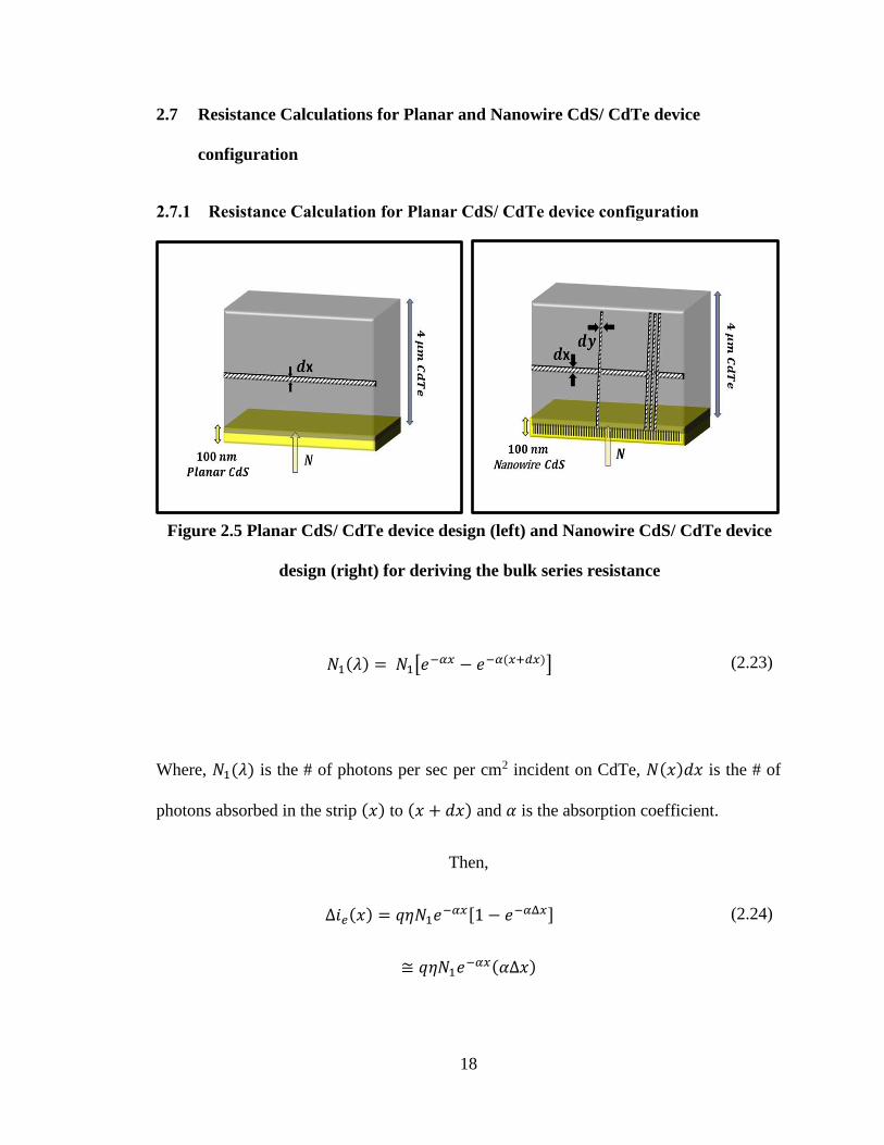
Figure 2.5 Planar CdS/ CdTe device design (left) and Nanowire CdS/ CdTe device design
(right) for deriving the bulk series resistance ................................................................... 18
Figure 2.6 Cross-Section view of the Nanowire CdS / Titania and CdTe interface ......... 20
Figure 2.7 Top view of the Nanowire CdS and Titania Nanotube interface for bulk series
resistance calculation ........................................................................................................ 20
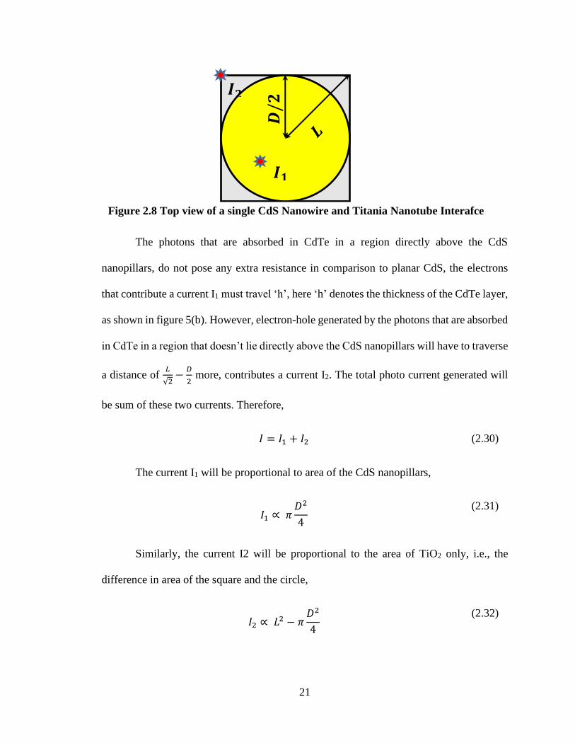
Figure 2.8 Top view of a single CdS Nanowire and Titania Nanotube Interafce ............. 21
Figure 3.1 LabView recorded - Anodization Current-time profile ................................... 26
Figure 3.2 Top view SEM image of TiO2 Nanotube anodized at 60V ............................. 29
Figure 3.3 Cross Section SEM image of TiO2 Nanotube anodized at 60V ...................... 29
Figure 3.4 1st cross section SEM image of CdS Nanowires embedded in TiO2 Nanotube
array .................................................................................................................................. 30
Figure 3.5 2nd cross section SEM image of CdS Nanowires embedded in TiO2 Nanotube
array .................................................................................................................................. 30
Figure 3.6 Absorption Curve generated from UV-Vis Spectroscopy data for Planar CdS
and TiO2 nanotubes with a porosity of 32%. ................................................................... 31
ix
Figure 3.7 Transmission Curve generated from UV-Vis Spectroscopy data for Planar CdS
and TiO2 nanotubes with a porosity of 32%. ................................................................... 31
Figure 5.1 Pauwells Vanhoutte Model for CdS/CdTe heterojunction .............................. 43
Figure 5.2 p-n heterojunction interface showing bending and discontinuities in bands ... 43
Figure 5.3 Solar Cell Definition ....................................................................................... 46
Figure 5.4 SCAPS: Action Panel ...................................................................................... 47
Figure 5.5 SCAPS: Solar Cell Definition Panel .............................................................. 48
Figure 5.6 SCAPS: Layer Properties Panel ...................................................................... 49
Figure 5.7 SCAPS: Defect Properties Panel ..................................................................... 50
Figure 5.8 SCAPS: Contact Panel .................................................................................... 51
Figure 5.9 SCAPS: Interface Panel ................................................................................... 52
Figure 5.10 SCAPS: I-V Panel ......................................................................................... 65
Figure 6.1 Top view SEM image of Sample # 1 fabricated in a fresh electrolyte comprising
of 98 mL of EG and 2 mL of NH4F at an anodization voltage of 50 V. .......................... 68
Figure 6.2 Top view SEM image of sample # 2 fabricated in a fresh electrolyte comprising
of 98 mL of EG and 2 mL of NH4F at an anodization voltage of 60 V. .......................... 69
Figure 6.3 Top view SEM image of sample # 3 fabricated in a fresh electrolyte comprising
of 98 mL of EG and 0.81 mL of NH4F at an anodization voltage of 50 V. ..................... 70
Figure 6.4 Top view SEM image of sample # 4 fabricated in a fresh electrolyte comprising
of 98 mL of EG and 0.3 mL of NH4F at an anodization voltage of 40 V. ....................... 71
Figure 6.5 Top view SEM image of sample # 5 fabricated in a fresh electrolyte comprising
of 98 mL of EG and 0.3 mL of NH4F at an anodization voltage of 50 V. ....................... 72

x
Figure 6.6 Top view SEM image of sample # 6 fabricated in a used electrolyte comprising
of 98 mL of EG and 0.3 mL of NH4F at an anodization voltage of 60 V. ....................... 73
Figure 6.8 Theoretical absorption profile CdS Nanowires for 80% - 100% coverage ..... 78
Figure 6.9 Theoretical absorption profile CdS Nanowires for 55% - 75% coverage ....... 79
Figure 6.11 Theoretical absorption profile CdS Nanowires for 5% - 25% coverage ....... 80
Figure 6.12 Jsc vs 1-100% CdS Coverage Interpore Distance 100nm ............................. 85
Figure 6.13 Jsc vs 0.0001-0.1% CdS Coverage Interpore Distance 100nm ..................... 87
Figure 6.14 Voc vs 1-100% CdS Coverage Interpore Distance 100nm ........................... 90
Figure 6.15 Voc vs 0.0001-0.1% CdS Coverage Interpore Distance 100nm .................... 91
Figure 6.16 FF vs 1-100% CdS Coverage Interpore Distance 100nm .............................. 93
Figure 6.17 FF vs 0.0001-0.1% CdS Coverage Interpore Distance 100nm ...................... 94
Figure 6.18 Efficiency vs 0.0001-0.1% CdS Coverage Interpore Distance 100nm .......... 96
Figure 6.7 Absorption vs Wavelength for 32% CdS Coverage Experimental vs Theoretical
............................................................................................................................................ 77
Figure 6.10 Theoretical absorption profile CdS Nanowires for 30% - 50% coverage ..... 79
Figure 6.19 Efficiency vs 1-100% CdS Coverage Interpore Distance 100nm .................. 97
1
CHAPTER 1. INTRODUCTION
The photovoltaic effect was discovered by Edmund Becquerel in 1839. Becquerel
while experimenting with an electrochemical cell consisting of a silver coated platinum
electrode immersed in electrolyte observed the generation of a weak electrical current
when the electrochemical cell was exposed to sunlight. However, it was not until 1954
when the first solar cell in the form of a diffused silicon p-n junction was developed by
Bell Labs researchers Chapin, Fuller, and Pearson [1], quickly followed by the works of
Reynolds, Leies, Antes, and Marburger [2] to develop cadmium sulfide (CdS) solar cell.
1.1 Status of Solar Photovoltaics
Conventional energy resources, such as fossil fuels, will be exhausted within the
next century. In addition, the increasingly serious environmental problems all over the
world have become a core driving force to promote renewable energy. The accelerated
global warming and climate change is one of them, primarily due to the large carbon
consumption from the burning of the fossil fuels since the Industrial Revolution. In 2016,
the world just passed the symbolic 400 parts per million (PPM) threshold of CO2
concentration, and the average temperature is also set to be the hottest year on record [3].
Therefore, renewable energy sources with low carbon emission is strongly desirable to
rectify this situation.
Solar photovoltaics (PV) is a very attractive renewable energy source. According
to one relevant study [4], PV installation on about 0.6% of the land in the US could be
enough to meet the entire country’s electricity need. Since the fabrication of PV modules
consumes energy, some people have questioned PV’s effectiveness on the reduction of

2
carbon emission. But this argument is not valid even for current PV technology. The
average energy payback time (i.e., the module power output time needed to compensate
the energy consumed for module production) of PV modules is ∼ 1 years and decreasing
with technology advances, but PV industry has widely guaranteed a 25-year product
lifetime (i.e., producing 80% of its power over 25 years).
However, it must be admitted that the stimulation of government incentives and
subsidies has been playing an important role in the PV market. To maintain a long-term
and sustainable growth, and to have a more influential impact on climate change, the solar
industry needs to rely less on the subsidies and develop economically competitive PV
electricity. Many countries such as Spain, Italy, Germany, UK, and Japan, have
encountered or are encountering a boom-bust cycle (i.e., with government subsidies, PV
installation grows very fast in the first few years; but the installation sharply decreases once
governments reduce or cut down the subsidies) due to a strong dependence of the subsidies
[5].
The advancement of PV technology can contribute to reduce the PV system cost.
That is to enable more efficient and durable PV products. For instance, First Solar, the
world largest thin-film CdTe PV manufacturer, has reduced the CdTe module
manufacturing cost from $1.02/Watt in 2010 to $0.51/Watt in 2015 [6] with its large
investment on R&D. Within only 5 years, its cell and module efficiencies have been
boosted from 16.5% to 22.1% and from 14.4% to 18.2% respectively [7]. The cost of PV
systems can be further reduced by improving the reliability and decreasing the degradation
rate of PV modules. The US National Renewable Energy Laboratory (NREL) has pointed

3
out that extending the PV system lifetime from a more standard expectation of 30 years to
50 years over long-term yields less PV system cost [8].
Overall, by taking its environment-friendly advantage, solar PV can play an
important role in mitigating or even reversing the worsening climate change. With more
efforts being made on technology improvements, it will possess more growth potential both
economically and environmentally.
1.2 Status of CdTe PV
Since this thesis has a focus on CdTe solar cells, this section will give a brief
summary of the current status and historic development of CdTe PV, and its advantages
and disadvantages compared to the traditional Si PV technology (broadly including
monocrystalline and polycrystalline Si). The research of CdTe-based PV devices began in
the early 1960s, studied with a variety of device structures including homojunctions,
heterojunctions, and Schottky barrier cells, and with efficiencies around 10% at that time
[9]. By the middle of the1990s, the cell efficiency increased to 15% for CdS/CdTe
heterojunction configuration [10]. Recently, the cell efficiency has broken the 20%
threshold by enhancing optical absorption and electrical properties [7]. As a result, the
CdTe-based PV technology has become a mainstream PV technology in part due to a
wealth of research advances. Today, First Solar has installed over 13.5 GW CdTe modules
worldwide and continues to grow with ∼3 GW of annual pipeline production [11].
Though the conventional Si PV technology occupies most of the PV market share,
CdTe technology still possesses compelling advantages compared to Si and has the
potential to increase the installation capacity. (1) The most obvious advantage of CdTe
4
over Si is a much lower material consumption due to its direct bandgap and thus high
absorption coefficient. The typical CdTe absorber layers are usually 1-4 µm thick, while
the crystalline Si wafers are over 100 µm thick. As a result, CdTe has a shorter energy
payback time than Si cells (∼2 years for silicon, but < 1 year for CdTe thin films) [12]. (2)
CdTe has less strict material purity requirement (i.e., 100 times less than Si) and simpler
manufacturing process than Si (i.e., the full process time: < 3.5 hours for CdTe but ∼ 3
days for Si) [7]. (3) Since CdTe has a superior temperature coefficient, better spectral
response, and better shading response, CdTe PV devices yield up to 12% higher energy
density than Si in abundant sunshine region [7]. Because of these advantages, the current
cost of CdTe module manufacturing is estimated to be $0.51/W, cheaper than Si with
$0.66-0.74/W.
1.3 Challenges in the CdTe technology
CdTe based thin film solar cells are very attractive because of their low cost and
relatively high efficiencies. CdTe has a close to optimal energy band gap of 1.5 eV for
solar cell applications and a relatively high absorption coefficient (α) value of 105 cm-1
[13]. Therefore, it serves as the absorber layer in n-CdS/p-CdTe heterojunction solar cells,
which is a leading thin-film solar cell technology today. Commercial CdTe cells have
already achieved a Power Conversion Efficiency (PCE) of 22.1% [7]. This was achieved
through increased scientific understanding and development of techniques including
cadmium chloride treatment, thinning of the CdS window layer, incorporation of an
interlayer between CdTe and the back electrode, and addition of a buffer layer between
5
CdS and the transparent electrode [14]. However, further improvements in PCE are needed
to bring down the cost of solar power in dollars per watt.
In the past decade, improvement of efficiency has mostly been achieved by
increasing short circuit current densities (Jsc). However, raising the Voc beyond 900 mV
has been a daunting challenge for the past two decades, due to several technical and
fundamental material limitations associated with CdTe. Metzger et al. [15] has shown that,
among the many characteristics of CdTe, including large lattice constant, low carrier
concentration stemming from doping difficulties, and the lack of suitable II-VI hetero-
partners to make ideal, lattice matched junctions, the most degrading is the excessively
large interface state concentration at the CdTe-CdS heterojunction. They were able to
demonstrate a Voc of higher than 1 V by using single crystal CdTe for the absorber material
in their cells. However, even though this single crystal technique is useful for research, it
is not very practical for large-scale production as of now.
1.4 Objectives of this Research Work: Optimal Nanostructures CdTe Solar Cells
Advantages of using nanostructures in solar cell design have been described in the
literature by the Ernst and Konnenkamp group [16], [17]. Also, earlier work in our
Electronic Devices Research Laboratory (EDRL) by Dang et al [14] has shown that the
performance output of CdS-CdTe solar cells can be enhanced by replacing the thin film
CdS window layer in the traditional device design by CdS nanopillars. The above
enhancement was demonstrated with CdS nanopillars of 60 nm diameter spaced to have a
neighbor center to center distance of 105 nm. However, the parameters affecting the power
conversion efficiency were not optimized because that was not the objective of their work.

6
In our research, an investigation was undertaken to study the various material and device
parameters like CdTe doping level, diameter of the CdS nanopillars and the neighbor center
to center distance for achieving the maximum solar cell power conversion efficiency in
these devices.
More specifically, the ultimate objective of the work presented in this thesis is to study
the effect of host nanotube parameters (pore diameter and pitch for different CdS
coverages) and CdTe doping density on device performance in nanowire CdS/ CdTe solar
cells using SCAPS-1D simulation, and to find the optimal set of conditions that will give
the highest efficiency employing the nanowire CdS/ CdTe device design. An overview of
the structure of the thesis is as follows:
i. Chapter 2 includes a description of the simple p-n junction theory. Bulk series
resistance formula for the case of planar and nanowire CdS device design have been
derived.
ii. Chapter 3 describes the experimental procedures and characterization techniques
used. The pore diameter, the pitch and the porosity for the fabricated devices are
investigated by SEM characterization. UV-VIS spectrophotometry measurements
of the fabricated devices are also presented.
iii. Chapter 4 reviews the nanoporous titania template and details the literature review
to understand the effect of various parameters influencing the formation of Titania
Nanotubes.
iv. Chapter 5 gives the description of the working of SCAPS-1D package.
v. Chapter 6 does the analysis of the results obtained.
vi. Chapter 7 discusses the conclusions and provides the suggestions for future work.

7
CHAPTER 2. SOLAR CELL THEORY
2.1 Photovoltaic Effect
The Photovoltaic Effect was discovered in 1839 by French Experimental Physicist
Edmund Becquerel. Becquerel while experimenting with an electrochemical cell
consisting of a silver coated platinum electrode immersed in electrolyte observed the
generation of a weak electrical current when the electrochemical cell was exposed to
sunlight.
2.2 Solar cell
The fundamental elements of a solar cell required for the conversion of light energy
into electrical energy owing to the photovoltaic effect are: (i) Junction, where the charge
separation of light induced electrons and holes occurs; (ii) Absorber material, where the
photons gets absorbed; and (iii) contacts, where the electrons and holes are collected to
give electrical current to drive the load.
A solar cell comprises of a p-n junction. The junction formed can be homojunction
or heterojunction. When the p-type and the n-type regions of the same semiconductor is
brought together gives rise to a homojunction. The built-in potential across the p-type and
the n-type semiconductor homojunction in thermal equilibrium is equal to the difference
in the work functions and is given by
𝑉𝑏𝑖 =
𝑘𝑇
𝑞𝑙𝑛 (
𝑁𝐴𝑁𝐷
𝑛𝑖2 ) (2.1)

8
Where 𝑁𝐴 and 𝑁𝐷 are the acceptor and the donor concentrations of the p-type and the n-
type semiconductor respectively and 𝑛𝑖 is the intrinsic carrier concentration of the
semiconductor.
This built-in potential gives rise to the electric field, which in turn separates the
light induced electrons and holes, when the solar cell is connected across the load.
The width of the depletion region which is a function of built-in potential, the
acceptor concentration and the donor concentration. For a two-sided abrupt junction, the
depletion width is given by
𝑊 = [2𝑉𝑏𝑖𝜀𝑠
𝑞(
1
𝑁𝐴+
1
𝑁𝐷)]
12 (2.2)
For a one-sided abrupt junction, the depletion width is given by
𝑊 = [2𝑉𝑏𝑖𝜀𝑠
𝑞𝑁𝐵]
12 (2.3)
Where 𝑁𝐵 = 𝑁𝐴 or 𝑁𝐷, depending on whether 𝑁𝐴>>𝑁𝐷 or 𝑁𝐴<<𝑁𝐷
When two semiconductor materials of different energy bandgaps are brought
together, the junction formed is termed as heterojunction. The quality of heterojunction
formed depends on (i) the electron affinities of the semiconductor materials, difference in
electron affinities can result in energy discontinuities in the energy bands; (ii) lattice
constant of the semiconductor materials; and (iii) the thermal expansion coefficients.
Interfacial dislocations at the interface gives rise to interface states which acts as trapping
centers, could result from the mismatch in lattice constant and thermal expansion
coefficients of the two semiconductor materials.

9
The built-in potential across the p-type and the n-type semiconductor
heterojunction in thermal equilibrium is equal to the difference in the work functions and
is given by
𝑉𝑏𝑖 = 𝐸𝑔2 − (𝐸𝑓 − 𝐸𝑐2) + 𝜒2 − 𝜒1 − (𝐸𝑐1 − 𝐸𝑓) (2.4)
Where 𝐸𝑔, 𝐸𝑓, 𝐸𝑐 and 𝜒 are the energy bandgap, fermi level, conduction band and the
electron affinity respectively for the semiconductor materials.
In a p-n junction diode in equilibrium, the net electron and hole current is zero.
There are internal electron diffusion current and electron drift current, but they are equal
and opposite. Therefore, the net electron current is zero. Similarly, net hole current is also
zero.
The light generated current is contributed by: (i) Holes generated in the n-region by
incident photons, (ii) Electrons generated in the p-region by incident photons and (iii)
Electron-hole pairs (EHP) generated in the depletion region by incident photons. At the
front surface the current is controlled by the surface recombination velocity, the surface
recombination current balances out the diffusion current from the n-region. The
photocurrent contribution from the electron-hole pairs in the depletion region is not
affected by recombination, the electric field is so high that the photogenerated electrons
and holes are immediately swept away by the electric field and there is no time for
recombination.

10
2.3 I-V Characteristics of a solar cell
Figure.2.1 I-V Characteristics of a solar cell under illumination
Figure.2.1 shows the typical I-V Characteristics of a solar cell under illumination
[19]. At higher illumination intensities the effect of high series resistance, 𝑅𝑠, becomes
more pronounced while at lower illumination intensities the effect of poor shunt resistance,
𝑅𝑠ℎ, is more predominant. The shunt resistance, 𝑅𝑠ℎ, value can be readily obtained from
the IV curve by taking the inverse of the slope of the IV curve in the third quadrant. The
series resistance, 𝑅𝑠, can be estimated by finding the inverse of the slope of the IV curve
at the open circuit voltage.
The dark I-V characteristics of the solar cell follow the ideal I-V characteristics of
a diode

11
𝐼 = 𝐼0 [𝑒𝑥𝑝
𝑞𝑉𝐹𝜂𝑘𝑇 − 1] (2.5)
Under illumination from sunlight
𝐼 = 𝐼0 [𝑒𝑥𝑝
𝑞𝑉𝐹𝜂𝑘𝑇 − 1] − 𝐼𝐿 (2.6)
Where IL is the light generated current.
2.4 p-n junction solar cell under illumination
The equivalent circuit of an ideal solar cell consists of a constant current source and
a diode.
Figure 2.2 Equivalent Circuit of an ideal solar cell
The equivalent circuit of a solar cell consists of a constant current source, a diode,
the series and shunt resistances associated with the diode.

12
Figure 2.3 Equivalent circuit of non-ideal device with finite series and shunt
resistances
Case I: Short Circuit
𝑉𝐹 = 0 gives
𝐼𝑆𝐶 = 𝐼𝐿 (2.7)
Case II: Open Circuit
𝐼 = 0 gives
𝑉𝑂𝐶 =
𝜂𝑘𝑇
𝑞ln (
𝐼𝐿
𝐼0+ 1) (2.8)

13
Case III: At load
Figure 2.4 Equivalent circuit of ideal Solar cell under illumination with load RL
𝐼 = 𝐼0 [𝑒𝑥𝑝𝑞𝑉𝐹𝜂𝑘𝑇 − 1] − 𝐼𝐿
(2.9)
and
𝑉 =
𝜂𝑘𝑇
𝑞ln (
𝐼𝐿
𝐼0+ 1) (2.10)
2.5 Maximum Power delivered to the load
Power delivered to the load
𝑃 = −𝑉𝐼 = (
𝜂𝑘𝑇
𝑞) 𝐼 ln (
𝐼𝐿
𝐼0+ 1) (2.11)

14
The power delivered would be maximum when
𝑑𝑃
𝑑𝐼= 0 (2.12)
The maximum current and maximum voltage are given by:
𝐼𝑚 = 𝐼0
𝑞𝑉𝑚
𝑘𝑇𝑒
𝑞𝑉𝑚𝜂𝑘𝑇 ≈ 𝐼𝐿 (1 −
𝜂𝑘𝑇
𝑞𝑉𝑚) (2.13)
𝑉𝑚 = 𝜂𝑘𝑇
𝑞𝑙𝑛 [
𝐼𝐿
𝐼0+ 1
1 +𝑞𝑉𝑚
𝜂𝑘𝑇
] ≈ 𝑉𝑂𝐶 −𝜂𝑘𝑇
𝑞𝑙𝑛 (1 +
𝑞𝑉𝑚
𝜂𝑘𝑇) (2.14)
The above equation is a transcendental equation. Its numerical solution yields the
value of 𝑉𝑚 that needs to be calculated using iterative method. Then 𝐼𝑚 is found by plugging
in the value of 𝑉𝑚. Once the values of 𝑉𝑚 and 𝐼𝑚 are obtained, those can be used to calculate
the maximum power delivered from the solar cell.
Maximum power obtained is given by:
𝑃𝑚 = 𝑉𝑚𝐼𝑚 = 𝑉𝑂𝐶 ∗ 𝐼𝑆𝐶 ∗ 𝐹𝐹
≈ 𝐼𝐿 [𝑉𝑂𝐶 −𝑞
𝜂𝑘𝑇𝑙𝑛 (1 +
𝑞𝑉𝑚
𝜂𝑘𝑇) −
𝜂𝑘𝑇
𝑞]
(2.15)

15
2.6 Solar cell Parameters
The performance of a solar cell is characterized in terms of open circuit voltage (𝑉𝑂𝐶),
short circuit current (𝐼𝑆𝐶) and the fill factor (FF). The product of these three quantities gives
the maximum power output of the device.
2.6.1 Open Circuit Voltage
The open-circuit voltage of a solar cell is given by
𝑉𝑂𝐶 =
𝜂𝑘𝑇
𝑞ln (
𝐽𝑆𝐶
𝐽0+ 1) (2.16)
Where 𝜂 is the diode ideality factor, 𝑘 is the Boltzmann constant, 𝑇 is the operating
temperature, 𝑞 is the electronic charge, 𝐽𝑆𝐶 is the short circuit current density and 𝐽0 is the
saturation current density.
The saturation current density is given by
𝐽0 = 𝑞𝑁𝐶𝑁𝑉 (1
𝑁𝐴√
𝐷𝑛
𝜏𝑛+
1
𝑁𝐷√
𝐷𝑝
𝜏𝑝) 𝑒−
𝐸𝑔
𝑘𝑇 (2.17)
Where 𝑁𝐶 is the density of states of the conduction band, 𝑁𝑉 is the density of states of the
valence band, 𝑁𝐴 is the acceptor density, 𝐷𝑛 is the diffusion length of electrons, 𝜏𝑛 is the
carrier lifetime of electrons, 𝑁𝐷 is the donor density, 𝐷𝑝 is the diffusion length of holes, 𝜏𝑝
is the carrier lifetime of holes and 𝐸𝑔 is the band gap of the absorber material.

16
2.6.2 Short Circuit Current density
The short-circuit current density over the entire solar spectrum is given by
𝐽𝑆𝐶 = ∫ (𝐽𝑛 + 𝐽𝑝 + 𝐽𝑑) 𝑑𝜆 ≅ 𝑞
𝜆𝑚𝑎𝑥
𝜆𝑚𝑖𝑛
∫ 𝐹(1 − 𝑅)
𝜆𝑚𝑎𝑥
𝜆𝑚𝑖𝑛
𝑑𝜆 (2.18)
Where 𝜆𝑚𝑖𝑛 is 0.3 µm for sunlight, 𝜆𝑚𝑎𝑥 is the wavelength corresponding to the absorption
edge of the absorber material, 𝐽𝑛 is the electron current density, 𝐽𝑝 is the electron current
density, 𝐽𝑑 is the photocurrent density in the space charge region, 𝐹 is the incident photon
flux and 𝑅 is the reflectivity of the light at the surface. The approximation in the above
equation is valid when the diffusion length (L) is very large such that αL>>1, where α is
the absorption coefficient of the absorber material.
2.6.3 Fill Factor
Fill Factor represents how close the real solar cell is to ideal solar cell and is a
measure of the "squareness" of the IV curve and represents the area of the largest rectangle
that will fit the IV curve. FF is defined as the ratio of maximum power from the solar cell
to the product of 𝑉𝑂𝐶 and 𝐼𝑆𝐶 .
𝐹𝐹 =
𝑃𝑚𝑝
𝑉𝑂𝐶 ∗ 𝐼𝑆𝐶=
𝑉𝑚𝑝 ∗ 𝐼𝑚𝑝
𝑉𝑂𝐶 ∗ 𝐼𝑆𝐶 (2.19)
Where 𝑃𝑚𝑝 is the maximum power delivered from the solar cell, 𝑉𝑚𝑝 is the voltage at the
maximum power point and 𝐼𝑚𝑝 is the current at the maximum power point.
When the parasitic series resistance and shunt resistance, 𝑅𝑠 and 𝑅𝑠ℎ, both have
negligible effect on the solar cell performance, the fill factor can be approximately
expressed in terms of open-circuit voltage as [18]

17
𝐹𝐹 =
𝑞𝑉𝑂𝐶
𝑘𝑇− 𝑙𝑛 (0.72 +
𝑞𝑉𝑂𝐶
𝑘𝑇)
1 +𝑞𝑉𝑂𝐶
𝑘𝑇
(2.20)
However, when either the series resistance or the shunt resistance has significant
effect on the device performance the above equation may yield inaccurate results.
2.6.4 Power Conversion Efficiency
Power conversion efficiency (PCE): Power conversion efficiency is defined as the
ratio of maximum power that the solar cell can deliver to the incident power from the
incoming solar radiation.
𝑃𝐶𝐸 (𝜂) =𝑃𝑚(𝑀𝑎𝑥𝑖𝑚𝑢𝑚 𝑃𝑜𝑤𝑒𝑟 𝑡ℎ𝑎𝑡 𝑡ℎ𝑒 𝑠𝑜𝑙𝑎𝑟 𝑐𝑒𝑙𝑙 𝑐𝑎𝑛 𝑑𝑒𝑙𝑖𝑣𝑒𝑟)
𝐼𝑛𝑐𝑖𝑑𝑒𝑛𝑡 𝑃𝑜𝑤𝑒𝑟 𝑓𝑟𝑜𝑚 𝑆𝑢𝑛𝑙𝑖𝑔ℎ𝑡
=𝑉𝑂𝐶 ∗ 𝐼𝑆𝐶 ∗ 𝐹𝐹
𝑃𝑖𝑛𝑐
(2.21)
Where 𝑃𝑖𝑛𝑐 is the incident power from the incoming solar radiation and is given by
𝑃𝑖𝑛𝑐 = 𝐴 ∫ 𝐹(𝜆) (ℎ𝑐
𝜆)
∞
0
𝑑𝜆 (2.22)
A is the total device area, 𝐹(𝜆) is the incident photon flux and (ℎ𝑐
𝜆) is the energy
associated with each photon.
18
2.7 Resistance Calculations for Planar and Nanowire CdS/ CdTe device
configuration
2.7.1 Resistance Calculation for Planar CdS/ CdTe device configuration
𝑁1(𝜆) = 𝑁1[𝑒−𝛼𝑥 − 𝑒−𝛼(𝑥+𝑑𝑥)] (2.23)
Where, 𝑁1(𝜆) is the # of photons per sec per cm2 incident on CdTe, 𝑁(𝑥)𝑑𝑥 is the # of
photons absorbed in the strip (𝑥) to (𝑥 + 𝑑𝑥) and 𝛼 is the absorption coefficient.
Then,
Δ𝑖𝑒(𝑥) = 𝑞𝜂𝑁1𝑒−𝛼𝑥[1 − 𝑒−𝛼Δ𝑥] (2.24)
≅ 𝑞𝜂𝑁1𝑒−𝛼𝑥(𝛼Δ𝑥)
Figure 2.5 Planar CdS/ CdTe device design (left) and Nanowire CdS/ CdTe device
design (right) for deriving the bulk series resistance
19
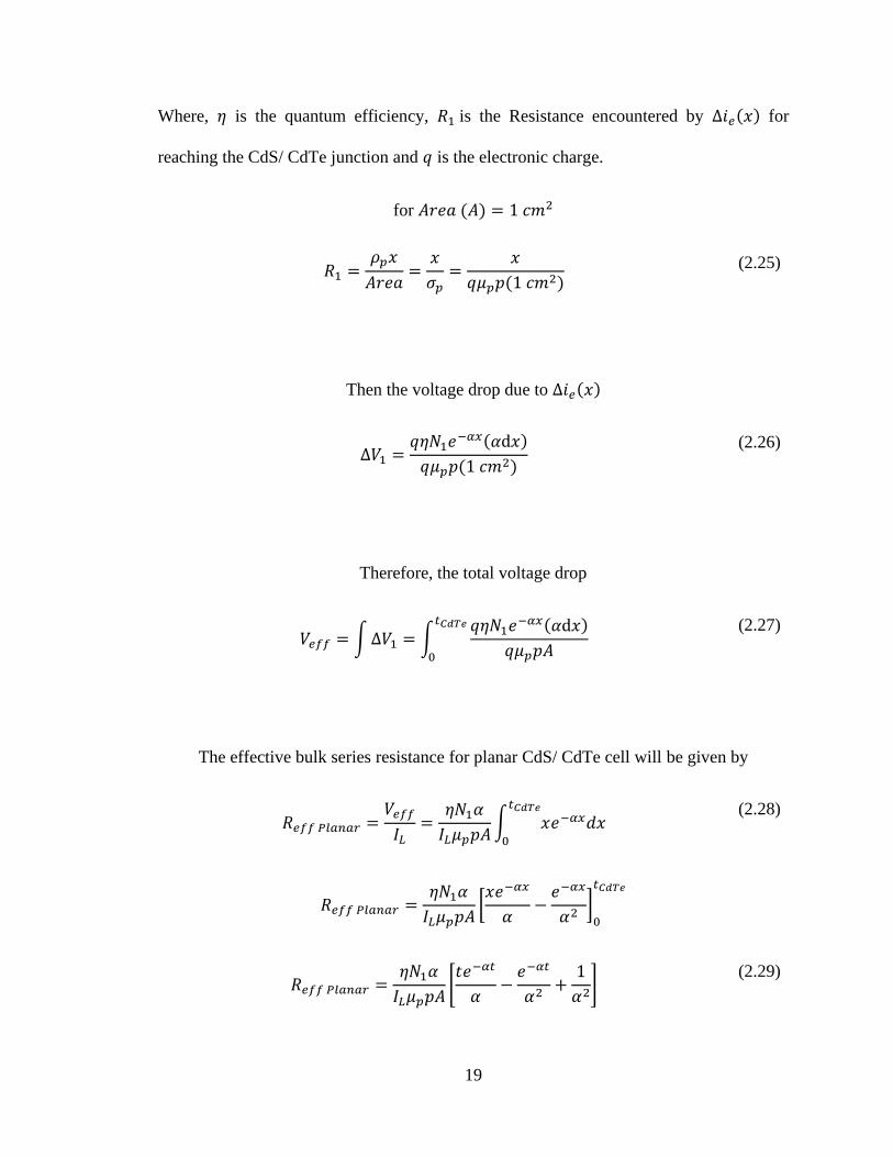
Where, 𝜂 is the quantum efficiency, 𝑅1 is the Resistance encountered by Δ𝑖𝑒(𝑥) for
reaching the CdS/ CdTe junction and 𝑞 is the electronic charge.
for 𝐴𝑟𝑒𝑎 (𝐴) = 1 𝑐𝑚2
𝑅1 =𝜌𝑝𝑥
𝐴𝑟𝑒𝑎=
𝑥
𝜎𝑝=
𝑥
𝑞𝜇𝑝𝑝(1 𝑐𝑚2)
(2.25)
Then the voltage drop due to Δ𝑖𝑒(𝑥)
Δ𝑉1 =𝑞𝜂𝑁1𝑒−𝛼𝑥(𝛼d𝑥)
𝑞𝜇𝑝𝑝(1 𝑐𝑚2)
(2.26)
Therefore, the total voltage drop
𝑉𝑒𝑓𝑓 = ∫ Δ𝑉1 = ∫𝑞𝜂𝑁1𝑒−𝛼𝑥(𝛼d𝑥)
𝑞𝜇𝑝𝑝𝐴
𝑡𝐶𝑑𝑇𝑒
0
(2.27)
The effective bulk series resistance for planar CdS/ CdTe cell will be given by
𝑅𝑒𝑓𝑓 𝑃𝑙𝑎𝑛𝑎𝑟 =𝑉𝑒𝑓𝑓
𝐼𝐿=
𝜂𝑁1𝛼
𝐼𝐿𝜇𝑝𝑝𝐴∫ 𝑥𝑒−𝛼𝑥𝑑𝑥
𝑡𝐶𝑑𝑇𝑒
0
(2.28)
𝑅𝑒𝑓𝑓 𝑃𝑙𝑎𝑛𝑎𝑟 =𝜂𝑁1𝛼
𝐼𝐿𝜇𝑝𝑝𝐴[𝑥𝑒−𝛼𝑥
𝛼−
𝑒−𝛼𝑥
𝛼2]
0
𝑡𝐶𝑑𝑇𝑒
𝑅𝑒𝑓𝑓 𝑃𝑙𝑎𝑛𝑎𝑟 =𝜂𝑁1𝛼
𝐼𝐿𝜇𝑝𝑝𝐴[𝑡𝑒−𝛼𝑡
𝛼−
𝑒−𝛼𝑡
𝛼2+
1
𝛼2]
(2.29)

20
The expression above gives the effective bulk series resistance encountered by the
window-absorber layer in the conventional CdS/ CdTe device configuration.
2.7.2 Resistance Calculation for Nanowire CdS/ CdTe device configuration
𝒉
𝑳/√𝟐
Figure 2.6 Cross-Section view of the Nanowire CdS / Titania and CdTe interface
Figure 2.7 Top view of the Nanowire CdS and Titania Nanotube interface for bulk
series resistance calculation
21
The photons that are absorbed in CdTe in a region directly above the CdS
nanopillars, do not pose any extra resistance in comparison to planar CdS, the electrons
that contribute a current I1 must travel ‘h’, here ‘h’ denotes the thickness of the CdTe layer,
as shown in figure 5(b). However, electron-hole generated by the photons that are absorbed
in CdTe in a region that doesn’t lie directly above the CdS nanopillars will have to traverse
a distance of 𝐿
√2−
𝐷
2 more, contributes a current I2. The total photo current generated will
be sum of these two currents. Therefore,
𝐼 = 𝐼1 + 𝐼2 (2.30)
The current I1 will be proportional to area of the CdS nanopillars,
𝐼1 ∝ 𝜋𝐷2
4
(2.31)
Similarly, the current I2 will be proportional to the area of TiO2 only, i.e., the
difference in area of the square and the circle,
𝐼2 ∝ 𝐿2 − 𝜋𝐷2
4
(2.32)
𝑫/𝟐
𝑰𝟏
𝑰𝟐
Figure 2.8 Top view of a single CdS Nanowire and Titania Nanotube Interafce

22
Considering the resistance offered to the electron-hole pairs generated directly
above the CdS nanopillar is R1. The extra resistance offered by the electron-hole pairs
generated above the non-CdS region for travelling a distance 𝐿
√2−
𝐷
2 more will be
𝜟𝑅 = 𝑅1 (𝐿
√2−
𝐷
2) ∗
1
ℎ
(2.33)
The total effective resistance offered to the electron-hole pairs that are generated in
a region that does not lie directly above the CdS nanopillar will be
𝑅2 = 𝑅1 + 𝛥𝑅 = 𝑅1 (𝐿
√2−
𝐷
2) ∗
1
ℎ
(2.34)
Now, the effective resistance offered by nanostructured configuration is given by
𝑅𝑒𝑓𝑓 𝑛𝑎𝑛𝑜𝑤𝑖𝑟𝑒 =𝐼1𝑅1 + 𝐼2𝑅2
𝐼1 + 𝐼2
(2.35)
𝑅𝑒𝑓𝑓 𝑛𝑎𝑛𝑜𝑤𝑖𝑟𝑒 =
𝑅1 [1 +𝜋𝐷2
4 [𝐿2 −𝜋𝐷2
4 ]] ∗ [1 + (
𝐿
√2−
𝐷2
) ∗1ℎ
]
[1 +𝜋𝐷2
4 [𝐿2 −𝜋𝐷2
4 ]]
(2.36)
Therefore, the effective nanowire resistance will be given by
𝑅𝑒𝑓𝑓 𝑛𝑎𝑛𝑜𝑤𝑖𝑟𝑒 = 𝑅1 ∗ [1 + (𝐿
√2−
𝐷
2) ∗
1
ℎ]
(2.37)
𝑅𝑒𝑓𝑓 𝑛𝑎𝑛𝑜𝑤𝑖𝑟𝑒
𝑅𝑒𝑓𝑓 𝑃𝑙𝑎𝑛𝑎𝑟= [1 + (
𝐿
√2−
𝐷
2) ∗
1
ℎ]
(2.38)

23
CHAPTER 3. EXPERIMENTAL PROCEDURES & OPTICAL CHARACTERIZATION
3.1 Experimental Procedures
3.1.1 Substrate Cleaning
Commercially available Indium Tin Oxide (ITO) Soda Lime Glass Substrate (MSE
Supplies 80-85% Transmittance, sheet resistance 12-15 Ω/square, 25 x 25 x 1.1 mm) were
ultrasonicated in Acetone (Alfa Aesar ACS 99.5+%) bath and Isopropyl Alcohol (Fisher
Chemical, 2-Propanol Certified ACS Plus) bath for 30 minutes each. The samples were
then rinsed in de-ionized water and dried in nitrogen flow before the microwave induced
plasma etch cleaning.
3.1.2 Microwave Induced Plasma Etch
The ITO glass substrates post cleaning was subjected to microwave induced plasma
etch for 1 minute at 100% power in Argon gas. The samples were then masked using Al
foil, leaving out some area for ITO cathode, before sputtering.
3.1.3 RF Sputtering of Intrinsic Tin Oxide
100nm of Intrinsic Tin Oxide (SnO2, Goodfellow, 99.9%) was deposited by RF
magnetron sputtering using AJA Phase II J Sputtering System at the Center of Advanced
Materials (CAM) at the University of Kentucky. The deposition rate was maintained
around 1.587nm/min. The deposition parameters used during sputtering are given in Table
3.1. Highly resistive Intrinsic Tin Oxide acts as the buffer layer as they are known to
enhance the open circuit voltage (VOC) and fill factor (FF) when very thin film of CdS
window-layer is used in thin film CdTe solar cells [21].

24
3.1.4 DC Sputtering of Titanium
Titanium was also deposited using DC magnetron sputtering using AJA Phase II J
Sputtering System at the Center of Advanced Materials at the University of Kentucky.
Different deposition parameters used for depositing Titanium is shown in Table 3.1.
Table 3.1 Tin Oxide and Titanium Sputtering Parameters
Parameters Intrinsic Tin Oxide Titanium
Base Pressure 3-7 x 10⁻⁸ Torr 3-7 x 10⁻⁸ Torr
Deposition Pressure 3 mTorr 3 mTorr
Deposition Power 30 W 150 W
Deposition Time 63 minutes 36 minutes
Deposition Rate 1.58 nm/min 4.2 nm/min
Stage Temperature 24°C 300°C
Pre-Sputtering Time 2 minutes 2 minutes
3.1.5 Titania Nanotubes formation
The sputtered Titanium samples were used for converting Titanium to Titania
Nanotube array using anodic oxidation. The anodization solution consisted of 98 mL
Ethylene Glycol (Fisher, ACS Grade) and 0.3 mL Ammonium Fluoride (NH4F, 40% by
vol, JT Baker) in a PTFE beaker. PTFE beaker was first cleaned and dried in Nitrogen.
Then a half-inch magnetic stirrer was placed in the beaker. 98 mL of Ethylene Glycol was
measured and poured into the beaker. 0.3 mL of Ammonium Fluoride was mixed in
Ethylene Glycol with the help of a pipette using forward pipetting method. The solution
was mixed at 400 rpm for 30 minutes prior to performing any anodization of the Titanium
samples.
25
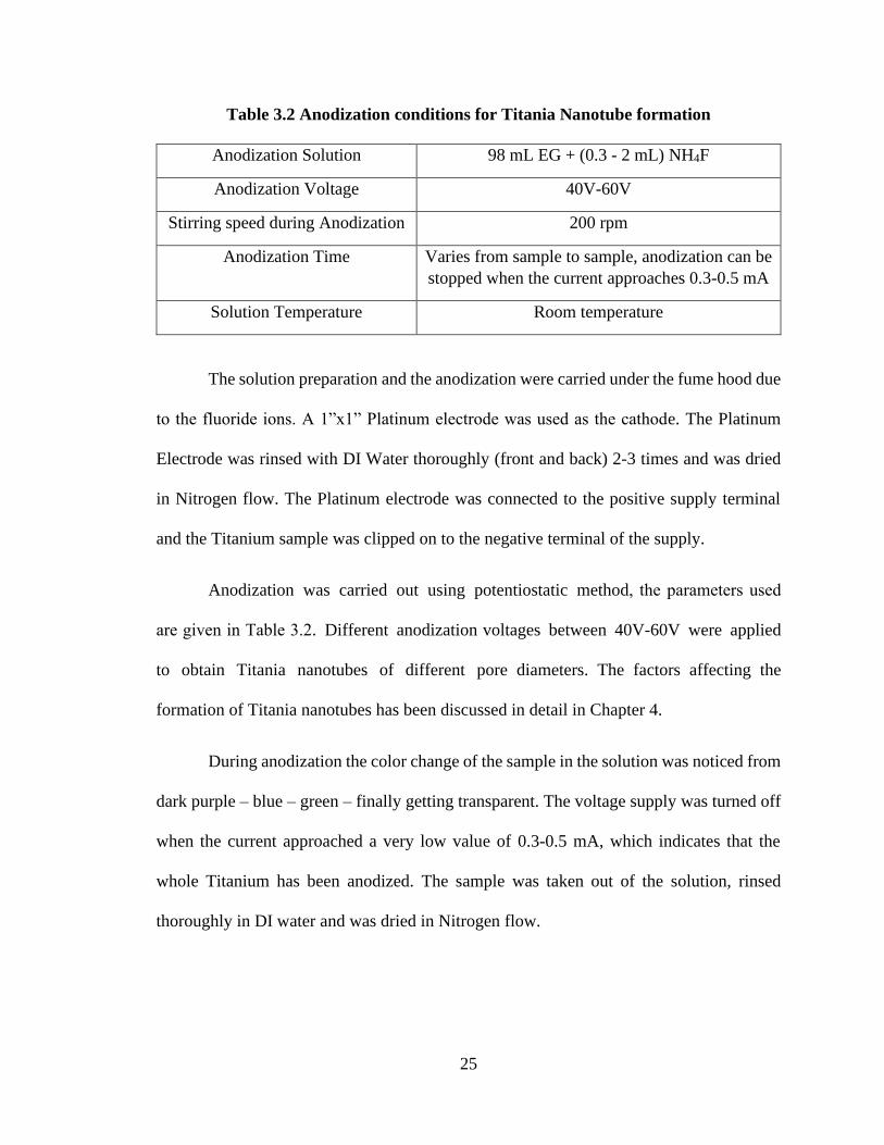
Table 3.2 Anodization conditions for Titania Nanotube formation
Anodization Solution 98 mL EG + (0.3 - 2 mL) NH4F
Anodization Voltage 40V-60V
Stirring speed during Anodization 200 rpm
Anodization Time Varies from sample to sample, anodization can be
stopped when the current approaches 0.3-0.5 mA
Solution Temperature Room temperature
The solution preparation and the anodization were carried under the fume hood due
to the fluoride ions. A 1”x1” Platinum electrode was used as the cathode. The Platinum
Electrode was rinsed with DI Water thoroughly (front and back) 2-3 times and was dried
in Nitrogen flow. The Platinum electrode was connected to the positive supply terminal
and the Titanium sample was clipped on to the negative terminal of the supply.
Anodization was carried out using potentiostatic method, the parameters used
are given in Table 3.2. Different anodization voltages between 40V-60V were applied
to obtain Titania nanotubes of different pore diameters. The factors affecting the
formation of Titania nanotubes has been discussed in detail in Chapter 4.
During anodization the color change of the sample in the solution was noticed from
dark purple – blue – green – finally getting transparent. The voltage supply was turned off
when the current approached a very low value of 0.3-0.5 mA, which indicates that the
whole Titanium has been anodized. The sample was taken out of the solution, rinsed
thoroughly in DI water and was dried in Nitrogen flow.

26
0 500 1000 1500 2000
0
5
10
15
20
Anodization Current-Time Curve
Time (Sec)
Cu
rren
t D
en
sit
y (
mA
/cm
2)
Figure 3.1 LabView recorded - Anodization Current-time profile
3.1.6 Annealing of as-anodized Titania Nanotubes
The as-anodized TiO2 nanotube samples were annealed for 2 hours in Oxygen
environment. The electrical and optical properties of Titania nanotubes are not influenced
significantly by the anodization conditions but can strongly modified by proper heat
treatment. The as-anodized Titania nanotubes are amorphous in nature and can be
converted to anatase or rutile crystalline form by heat treating at a suitable temperature.
Annealing between 350°C-450°C leads to predominant anatase form while annealing
beyond 450°C leads to rutile phase [20]. An increase in peak intensities are observed with
an increase in annealing time leading to better crystallized anatase or rutile structures [21].
Electrical conductivity of anatase phase is significantly higher than that of the rutile phase,
significant increase in conductivity after crystallization to anatase [22].
3.1.7 CdS Electrodeposition
The solution was first prepared by taking 50mL of Dimethyl Sulfoxide (DMSO)
into a beaker of suitable size. Prior to adding DMSO into the beaker half-inch magnetic

27
stirrer was cleaned and placed in the beaker. Then elemental Sulfur powder and Cadmium
Chloride powder were measured 0.5 gm each and were poured in the beaker containing
Dimethyl Sulfoxide. The beaker was placed on a hot plate and the hot plate was set to
150°C, close to the boiling point of DMSO. The temperature of the solution was monitored
using infrared thermometer. The solution was stirred at 300 rpm so that the solution is
mixed throughout.
Platinum electrodes which act as anode during electrodeposition was cleaned with
DI water and dried in Nitrogen flow. After cleaning, the Platinum electrode was connected
to the positive terminal of the supply. The TiO2 nanotubes samples obtained from the
previous step was connected to the negative terminal of the supply. The electrodes were
then immersed in the saturated solution of Cadmium Sulfide, stirring was stopped. A
current density of 7.5 𝑚𝐴/𝑐𝑚2 was applied to the electrodes during electrodeposition. A
constant DC current was applied for ~10 seconds to electrodeposit CdS into TiO2 nanotube
array.
When the deposition is complete the samples were taken out and rinsed with DI water
and were dried in Nitrogen. To enhance the crystallinity of the nanowire CdS the
electrodeposited CdS samples were heat treated in Argon environment at 385°C for 30
minutes.

28
3.2 Optical Characterization
3.2.1 Scanning Electron Microscopy
SEM images were taken using Hitachi S-4300 Scanning Electron Microscope and
FEI Helios Nanolab 660 in the Electron Microscopy Center (EMC) located at the
University of Kentucky.

29
Figure 3.2 Top view SEM image of TiO2 Nanotube anodized at 60V
Figure 3.3 Cross Section SEM image of TiO2 Nanotube anodized at 60V
30
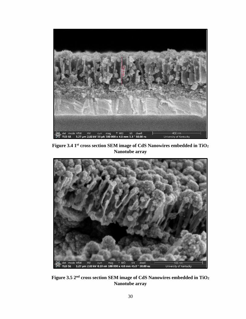
Figure 3.4 1st cross section SEM image of CdS Nanowires embedded in TiO2
Nanotube array
Figure 3.5 2nd cross section SEM image of CdS Nanowires embedded in TiO2
Nanotube array

31
3.2.2 UV-Vis Spectroscopy
Cary 50 UV-Vis Spectrophotometer was used to take the absorption and the
transmission data for the TiO2 nanotubes and Planar CdS.
Figure 3.6 Absorption Curve generated from UV-Vis Spectroscopy data for Planar
CdS and TiO2 nanotubes with a porosity of 32%.
Figure 3.7 Transmission Curve generated from UV-Vis Spectroscopy data for
Planar CdS and TiO2 nanotubes with a porosity of 32%.

32
CHAPTER 4. HOST NANO-POROUS TEMPLATE – TITANIA NANOTUBES
4.1 Nanoporous Titania
Titanium dioxide is one of the most studied metal oxides. It is also one of the most
explored nanomaterial based on transition metal oxides. Highly oriented vertically oriented
Titania nanotubes find its place in a variety of applications due as they provide large surface
to volume ratio, vertically aligned surface, excellent charge transfer properties in
nanomaterials mainly governed by the quantum confinement phenomenon. Various
methods have been evolved for fabricating TiO2 nanotubes including hydro/ solvothermal
techniques, template-assisted methods, seed growth method, sol-gel method and
electrochemical oxidation method.
Among these direct electrochemical oxidation turns out to be simplest and cheapest
way to fabricating TiO2 nanotubes. Zwilling et al. demonstrated that anodic oxidation of
Titanium foil leads to the formation of self-organized nanotubular structures of Titanium
dioxide [23]. Direct oxidation provides a controllable method of adjusting the shape, size
and the degree of order of the resulting in the formation of self-organized nanostructures.
Depending on the process parameters, direct oxidation of Titanium surface leads to the
formation of a compact structure, ranging from random porous structure to tubular
structure.
Porous Titania nanotubes can be fabricated by anodization of Titanium either in
acidic electrolytes or in basic electrolytes, either under potentiostatic or galvanostatic
conditions. Potentiostatic anodization is more widely used for the fabrication of self-
ordered porous Titania nanotubes. During potentiostatic anodization of Titanium, under

33
constant anodic potential a thin compact barrier oxide layer starts to grow over the
Titanium surface.
𝑇𝑖 + 2𝑂2− → 𝑇𝑖𝑂2 + 4𝑒− (4.1)
𝑇𝑖 + 2𝐻2𝑂 → 𝑇𝑖𝑂2 + 4𝐻+ + 4𝑒− (4.2)
The fabrication of Titania nanotube using anodic oxidation of Titanium has been
proposed to involve various stages of reactions [24] leading to the formation self-organized
nanostructures: (i) formation of oxide layer, (ii) pore formation and deepening of the pores,
(iii) incorporation of adjacent smaller pores into bigger pores, (iv) early nanotube array
formation and (v) formation of perfect nanotube array.
During the first stage of anodization the series resistance of the anodization circuit
increases over time with the thickening of the initial barrier oxide layer. After reaching a
certain thickness of the barrier oxide layer the current drops rapidly to reach a minimum
value which is the onset of second stage of anodization (pore initiation stage). For this
stage, the current concentrates on local imperfections existing on the initial barrier oxide
layer, resulting in non-uniform oxide thickening and pore initiation at the thinner oxide
areas [25].
Pore initiation in the growing anodic oxide starts as a result of morphological
instability. Pores develop from initial pits following the etching of the fluorine ion species
penetrating closer to the metal/ oxide interface. As the field-assisted fluorine ions starts to
etch the Titanium dioxide film more and more, the smaller pores start to merge and form
bigger pores. The process continues until an equilibrium is established between the

34
formation of Titanium dioxide and the etching of Titanium dioxide film, resulting in the
formation of perfectly well-aligned self-organized Titania nanotubes.
Nanotubular films of TiO2 fabricated in aqueous inorganic fluorine sources are
formed through the etching action of TiO2 by fluorine ions
𝑇𝑖𝑂2 + 𝑛𝐻2𝑂 + 6𝐹− → [𝑇𝑖𝐹6]2−+ (𝑛 + 2 − 𝑥)𝑂2−
+ 𝑥𝑂𝐻−
+ (2𝑛 − 𝑥)𝐻+
(4.3)
𝑇𝑖𝑂2 + 6𝐹− + (𝑛 − 𝑥)𝑂2−+ 𝑥𝑂𝐻− + (2𝑛 + 4 − 𝑥)𝐻+
→ [𝑇𝑖𝐹6]2−+ (𝑛 + 2)𝐻2𝑂
(4.4)
𝑇𝑖 + 𝑥𝑂𝐻− → 𝑇𝑖(𝑂𝐻)𝑥 + 𝑥𝑒− (4.5)
Where, n is used to describe the disassociation rate of water to dissolution of TiO2 and x is
used to describe the ratio of Titanium Hydroxides to TiO2.
The balance in the movement rates of the metal/ oxide interface and the oxide/
electrolyte interface governs the steady state pore growth and is achieved by a balance in
the dynamic equilibrium between the oxide dissolution at the oxide/ electrolyte interface
and formation of oxide at the metal/ oxide interface. Several theories have been proposed
to explain the steady-state pore formation mechanism such as average field model, Joule’s
heat-induced chemical dissolution model, field-assisted oxide dissolution model, direct
cation ejection mechanism and flow model.
35
Oxidation of Titanium
𝑇𝑖 → 𝑇𝑖4+ + 4𝑒− (4.6)
Anodic Oxidation
𝑇𝑖4+ + 2𝐻2𝑂 → 𝑇𝑖𝑂2 + 4𝐻+ (4.7)
Chemical Dissolution
𝑇𝑖𝑂2 + 6𝐹− + 4𝐻+ → [𝑇𝑖𝐹6]2−+ 2𝐻2𝑂 (4.8)
The most widely accepted theory for the Titania nanotube formation is the field
assisted oxide dissolution model [26, 27], which explains the early stage of the anodization
is breakdown of the TiO2 layer via the electric field. The balance between the oxide
formation, electric field driven inward movement of O2- ions and the outward migration of
Ti+ ions at the metal/ oxide interface, and the oxide dissolution maintains the barrier oxide
layer thickness. The ordering of pores is influenced by the magnitude of electrostatic stress
that is developed along the direction of the electric field as a result of the resistance
encountered due to the counter migration and attraction of the ions. Tubular TiO2
nanostructures of various lengths, pore diameters and wall thickness can be formed based
on optimal anodization parameters and solution composition.

36
4.2 Parameters influencing the formation of Titania Nanotubes by anodic
oxidation
The formation of Titania nanotubes using anodic oxidation of Titanium is influenced
by the electrolyte, water content, anodization voltage, electrodes, aged electrolyte,
anodization time, electrolyte temperature and the electrolyte pH.
4.2.1 Effect of electrolyte on anodic oxidation of Titanium
The nanotube array formation is significantly influenced by the composition and
concentration of the electrolyte used. There are four different generations of electrolyte
used for fabricating TiO2 nanotube arrays using anodic oxidation of Titanium. The first
generation of electrolyte used for fabricating TiO2 nanotube arrays were based on
hydrofluoric acid (HF)-based aqueous electrolytes. The relatively low pH in HF aqueous
solution electrolytes limited the length of the TiO2 nanotubes. High acidity of HF
electrolytes results in rapid dissolution of TiO2. The maximum nanotube length achieved
using the first generation of electrolyte was restricted to approximately 500nm [28-30].
The second generation used buffered electrolytes of citric acid or sodium sulfate by
adding weaker acids such as KF or NaF into buffered solution, also the pH was adjusted to
weakly acidic by addition of sulfuric acid or sodium hydroxide. By adjusting the pH to
weakly acidic of the electrolyte the nanotube of length approximately 4.4µm were achieved
[31]. In the second generation of electrolytes the pH interferes the electrochemical etching
and chemical dissolution leading to much longer nanotubes in acidic solutions.
The third-generation electrolytes used viscous polar organic electrolytes such as
glycerol, ethylene glycol, diethylene glycol, dimethyl sulfoxide (DMSO) in NH4F, NaF

37
and KF based fluoride media. The pore diameter in the third-generation electrolyte can be
influenced significantly by adjusting the fluoride ion concentration in the electrolyte.
Titania nanotube arrays with approximately 1000µm long were formed in ethylene glycol
containing 0.6 wt% NH4F and 3.5% water anodized at 60V for 216hr [32]. Ethylene glycol
electrolyte containing water and fluoride ions leads to double walled nanotube structures
[33].
The fourth-generation electrolytes use non fluoride-based electrolytes grow TiO2
nanotube arrays. Hydrochloric acid, Hydrogen peroxide, and their mixtures, Sodium
Chloride, perchloric acid solution and their mixtures and mixtures of Oxalic acid, formic
acid and sulfuric acid in ammonium chloride are used to replace the fluoride ions by
chloride ions to fabricate well-developed nanotube arrays [34,35-37]. For hydrochloric
acid-based electrolytes the only 3 M of acid concentration leads to the formation of
nanotube arrays [35].
4.2.2 Effect of water content on ethylene glycol based Titania nanotubes
The reproducibility of the formation of well-ordered Titania nanotube arrays in a
two-electrode configured anodization is affected by the water content of the electrolyte,
especially when the anodization is carried out for a shorter period of time. The initial water
content in the electrolyte is the key to getting reproducible results. The limiting anodization
potential can be varied by varying the water content in ethylene glycol-based electrolyte.
The initial current density in anodization decreases as the water content in the electrolyte
increases. A minimum of 0.18 wt% of water is required to from well-ordered Titania
nanotube arrays [38]. When the water content is greater than 0.5 wt%, the amount of ridges
38
on the circumference of the nanotubes increased [38]. The key to achieve very long
nanotubes is limiting the water content < 5% in the anodization bath [39].
The photoelectrochemical properties of Titania nanotubes can be modified by
varying the water content of the anodization electrolyte. Maximum photon to current
conversion efficiency was achieved using 10 wt% water in ethylene glycol based Titania
nanotubes, however, the higher water content in the electrolyte lead to ridged structures of
TiO2 nanotubes that are completely separate from each other [40].
4.2.3 Effect of anodization voltage
Anodization voltage is a critical parameter that strongly influences the pore
diameter and the interpore distance. Well-ordered TiO2 nanotubular structures can be
grown by applying a suitable range of voltage, below the limiting anodization potential,
across the electrodes. Various studies have been performed to study the effect of applied
voltage on the growth of TiO2 nanotubes. Z. Lockman et al. observed that the pore diameter
and the nanotube length increased with the increase in the anodization potential [41]. After
a certain point further increase in anodization potential lead to the deterioration of the
nanotubular structure forming a spongy-like structure or just randomly porous TiO2.
Y. Alivov et al. reported that the anodization potential does not have any clear
dependence on the pore diameter of the TiO2 nanotubes in glycerol-based electrolyte when
the anodization voltage was varied over the range of 10-240V. The average pore diameter
of 220nm was obtained for 10V, while, the samples grown at 30V, 60V and 120V had the
average pore diameter of 86nm, 156nm and 75nm respectively [42].
39
4.2.4 Effect of electrodes
A variety of electrode materials have been used as the cathode material in the
formation of TiO2 nanotubes including Ni, Pd, Pt, Fe, Co, Cu, Ta, W, C, Al and Sn in both
aqueous and ethylene glycol electrolytes [43]. Different cathode material affects the
dissolution kinetics of the Titanium anode leading to formation of TiO2 nanostructures of
different morphologies. The electrical conductivity of the electrolyte increases with the
amount of Titanium dissolved in the solution which in turn helps to prevent the debris
formation.
The aspect ratio of the TiO2 nanotubes vary significantly with the use of different
cathode material as counter electrode. Sreekantan et al. used iron, carbon, stainless steel
and aluminum as the counter electrodes and observed that TiO2 nanotubes formed using
stainless steel counter electrode produced shorter tube lengths that where conical in shape
and are unstable while TiO2 nanotubes formed using iron counter electrode produced well-
organized nanotubes of the higher aspect ratio is obtained [44].
4.2.5 Effect of aged electrolyte
Aged ethylene glycol electrolyte when reused leads to the formation of nanotubes
with reasonable quality (i.e. without unwanted debris, or porous oxide layers on the top of
the nanotube layer) [45]. Longer nanotubes are obtained in the solution that was previously
used to perform anodization. The breakdown potential, after which no ordered nanotubular
structures are obtained, increases with the aging of the electrolyte [46]. However, when the
solution is really aged leads to the formation of passive oxide layer instead of nanotubular
structure suggesting the depletion of the in 𝐹− and 𝐻+ions.

40
Aged electrolytes used for subsequent anodization leads to the formation low aspect
ratio nanotube arrays. In aged electrolyte subsequent anodization take longer time to
completely anodize same thickness of Titanium samples. The pore diameter increases
while the final nanotube length decreases in aged electrolyte than in fresh electrolyte when
anodization is performed in otherwise similar anodization conditions.
4.2.6 Effect of anodization time
Anodization time greatly influences the formation mechanism of TiO2 nanotube
formation. Too short of anodization does not lead to any nanotube formation. The
dimensions of the TiO2 nanotubes increases by extending the anodization time, however,
the average growth rate decreases [47]. Longer anodization time leads to the formation of
rough and cross-linked structure is seen where TiO2 nanotubes are clustered in groups or
bundles while shorter anodization time results in the formation of more organized TiO2
nanostructure [48]. Prolonging the anodization leads to the collapse of the nanotubular
structures starting with the thinning of tube walls due over dissolution of the tubes by the
fluoride ions.
4.2.7 Effect of electrolyte temperature
The rate of oxide growth, structural formation and the quality of TiO2 nanotubes is
directly influenced by the electrolyte temperature. The electrolyte temperature has a
significant impact on the dimensions (pore diameter and the wall thickness) of the
nanotubes formed in viscous non aqueous electrolytes, the nanotube size reduces with the
reduction in the electrolyte temperature, while in aqueous electrolytes the impact of
electrolyte temperature was insignificant [49].
41
However, Grzegorz D. Sulka et al. observed that the highest values of inner pore
diameter, pore circularity and the regularity in the pore arrangement are observed at an
optimal electrolyte temperature and applied potential of 20°C and 50V [50]. When the
electrolyte temperature was increased to 30°C smaller pore diameters, smaller pore
circularities and a weaker pore arrangement was seen [51].
4.2.8 Effect of electrolyte pH
The electrolyte pH in electrochemical anodization is an important parameter that
directly influence the formation of TiO2 nanotube structure by anodic oxidation of
Titanium. The fluoride ion concentration and the solution acidity determine the rate of
chemical dissolution of titania in the solution. The chemical dissolution increases with the
increase in 𝐹− and 𝐻+ concentration in the electrolyte. The acid in the electrolyte increases
the chemical dissolution as well as reduces the viscosity of the solution leading to fast
formation of Titania nanotubes.
The lower pH of the solution is known to prolong the time required to establish
equilibrium the dissolution rate and the rate of nanotube growth which in turn results in
increased pore diameter of the nanotubes [52]. The lower pH leads to increased pore
diameter but gives less ordered TiO2 nanotubes than that formed in pH neutral solutions.
Varying the pH from strongly acidic (pH<1) to weakly acidic (pH 4.5) increases the
nanotube length from 0.56 µm to 4.4 µm in otherwise similar anodizing conditions [53].
The wall thickness is increased as the pH increases up to pH value of 10 above that
the wall thickness, the pore diameter and the structural order of the nanotube decreases
gradually resulting in the formation of unwanted debris [53]. The lower pH values produce
shorter and cleaner nanotubes.

42
CHAPTER 5. NUMERICAL PROCEDURES AND SCAPS SIMULATION
SCAPS is a one-dimensional solar cell simulation program, originally developed for
cell structures of the CuInSe2 and the CdTe family. The program has evolved its
capabilities over time making it suitable for simulating crystalline solar cells (Si and GaAs
family) and amorphous cells (a-Si and micromorphous Si) [54]. SCAPS allows to add up
to seven semiconductor layers, Eg, χ, ε, NC, NV, vthn, vthp, μn, μp, NA, ND, all traps (defects)
Nt can be graded for each semiconductor layer. The different recombination mechanisms
included are band-to-band (direct), Auger, SRH-type. Intra band tunneling, tunneling to
and from interface states can be accounted for in the program.
A variety of illumination spectra are included, and it can also be supplied by the user.
The illumination can be from either the p-side or the n-side, also, allowing for spectrum
cut-off and attenuation. The generation is either calculated from the specified illumination
spectrum or can be user specified. The program calculates energy bands, concentrations
and currents at a given working point (voltage, frequency, temperature), J-V
characteristics, ac characteristics, spectral response. SCAPS also has a built-in curve fitting
feature and also a panel for the interpretation of admittance measurements.
In SCAPS the only variables to have explicit temperature dependence are the effective
density of states of the conduction band, the effective density of states of the valence band,
the thermal velocities, the thermal voltage and all their derivatives. The user must specify
the other corresponding material parameters for each T for other variables. The working
point voltage is the dc-bias voltage used in C-f simulation and in QE(λ) simulation. The
working point frequency the frequency at which the C-V measurement is simulated.

43
5.1 The Physical Model
The physical model in SCAPS is based on Pauwels Vanhoutte model [55]. The
figure 5.1 shows the interface recombination as the dominant recombination path between
the window electrons and the absorber holes. Pauwels Vanhoutte model considers the
interface recombination and arbitrary energy barriers at the interface to find the optimum
structure for a heterojunction solar cell.
The model is based on the various underlying assumptions as stated: (i) The
generation and recombination of carriers in the space charge region is neglected. (ii)
Thermionic emission is considered as the majority carrier transport mechanism in the space
charge region and it was assumed that at the interface one type of carriers are the majority
carriers. (iii) Interface recombination allows for the exchange of electrons and holes from
both conduction bands to the valance bands of both the semiconductors at the interface and
Figure 5.1 Pauwells Vanhoutte Model for
CdS/CdTe heterojunction
Figure 5.2 p-n heterojunction interface
showing bending and discontinuities in
bands

44
it was assumed that one of the semiconductors is much more heavily doped than the other.
(iv) Tunnelling at the interfaces or at the is neglected. (v) Analysis of efficiency is on the
basis of current-voltage characteristics.
The model, at the interfaces, allows for the discontinuities in (i) the quasi-fermi
levels, (ii) the energy bands Ec and Ev, and (iii) the bandgap Eg; for the interface
recombination to occur. Interface recombination is described by the extension of SRH
formalism. At the interfaces the electrostatic potential is assumed to be continuous.
Thermionic emission is used to derive the relation between fermi level discontinuity,
carrier concentrations and current. For direct bandgap semiconductors with identical
effective masses, the thermionic emission current for the electrons is given by
𝐽𝑡ℎ 𝑛 = 𝑣𝑡ℎ 𝑛 (𝑛1 exp (−|Δ𝐸c|
𝑘𝑇) − 𝑛2)
(5.1)
Where, 𝐽𝑡ℎ 𝑛 is the particle current from semiconductor 1 to 2, 𝑣𝑡ℎ 𝑛 is the thermal velocity
of electrons, 𝑛1 and 𝑛2 are the electron concentrations and Δ𝐸c is the discontinuity in the
conduction band. Thermionic emission current for holes can be computed similarly.
In SCAPS for each layer, the type and density of on shallow level and up to three
deep levels can be defined. The shallow level is completely ionized and does not contribute
to recombination. Transport of majority carriers and the minority carriers at the contacts is
described by thermionic emission and the surface recombination velocities respectively.
Boundary conditions are imposed on the continuity equation for the electrons at the metal
semiconductor contact
𝐽𝑛 = 𝑆𝑛(𝑛 − 𝑛𝑒𝑞) (5.2)

45
𝑆𝑛 = 𝐴∗𝑇2
𝑞𝑁𝑐= 𝑣𝑡ℎ 𝑛
(5.3)
Where, 𝑛𝑒𝑞 is the equilibrium electron concentration at the contact, 𝑆𝑛 is the surface
recombination velocity of electrons and 𝐴∗ is the effective Richardson constant.
Figure 5.2 shows the p-n heterojunction interface, where V1 and V2 are the band bendings
in the space charge regions of the p-type and the n-type semiconductor respectively, ΔEc
and ΔEv are the the discontinuities in the bands, EFn and EFp are the quasi-fermi levels under
forward bias V. jn, js2, js1 and j0n are electron particle current densities respectively entering
the space charge region of the n-type material, recombining from the conduction bands 1
and 2 at the interface, and leaving the space charge region of the p-type material. The
quantities jp, js1’, js2’ and j0p are hole particle current densities defined analogously. Fn and
Fp determine the doping concentrations.
The difference in electron-affinities of both materials determines the jump ΔEc in
the bottom of the conduction bands of the two semiconductors at the interface. ΔEv is the
jump in the top of the valence bands in the two semiconductors. ΔEv = ΔEc + ΔEg where
ΔEg = Eg2 - Eg1 is the difference in the bandgaps of the two semiconductors. ΔEc and ΔEv
can be positive or negative.
Using the Pauwels Vanhoutte model, it was concluded that for the heterojunctions
the semiconductor with the smaller bandgap should have good quality, i.e., it should have
larger collection efficiency; it should absorb all photons. Best efficiencies are obtained for
three type of device structures. In the first type, the weakly doped semiconductor should
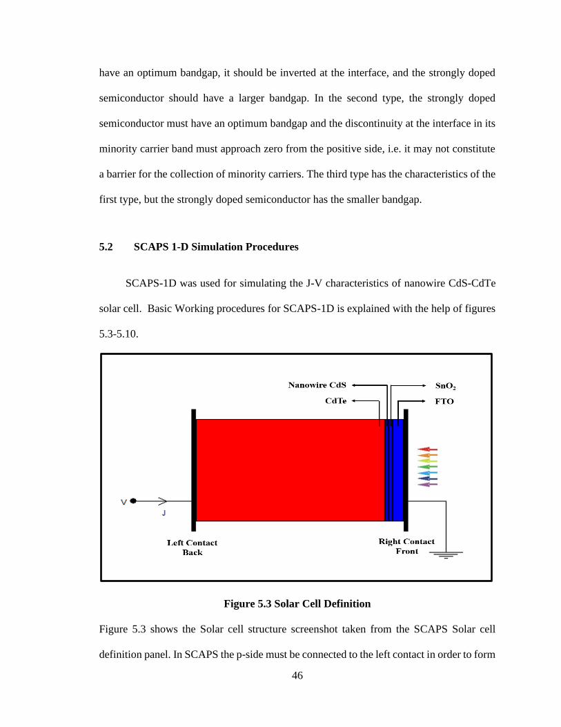
46
have an optimum bandgap, it should be inverted at the interface, and the strongly doped
semiconductor should have a larger bandgap. In the second type, the strongly doped
semiconductor must have an optimum bandgap and the discontinuity at the interface in its
minority carrier band must approach zero from the positive side, i.e. it may not constitute
a barrier for the collection of minority carriers. The third type has the characteristics of the
first type, but the strongly doped semiconductor has the smaller bandgap.
5.2 SCAPS 1-D Simulation Procedures
SCAPS-1D was used for simulating the J-V characteristics of nanowire CdS-CdTe
solar cell. Basic Working procedures for SCAPS-1D is explained with the help of figures
5.3-5.10.
Figure 5.3 Solar Cell Definition
Figure 5.3 shows the Solar cell structure screenshot taken from the SCAPS Solar cell
definition panel. In SCAPS the p-side must be connected to the left contact in order to form

47
a p-n junction due to the fact that n-p junction simulated in SCAPS leads to non-uniform
current which in turn is much less stable. SCAPS simulation program was used to simulate
window/ absorber type CdS/ CdTe solar cell. The p-side semiconductor used for simulation
is 5 𝜇𝑚 CdTe which acts as the absorber layer, while the n-side in 200nm Nanowire CdS
which acts as window layer. 100nm of intrinsic SnO2, which acts as a buffer layer, was
included to perform simulations for simulate for the actual device design used in our lab.
The solar cell is illuminated from the right side.
Figure 5.4 SCAPS: Action Panel
Figure 5.4 shows the SCAPS start-up panel is the Action panel. The action panel consists
of 5 blocks: Block 1 defines the problem; block 2 defines the working points; block 3 lets
the user to select the measurement(s) to simulate from I-V, C-V, C-f and QE(λ); block 4 is
for starting the calculation which can either be a single shot calculations or a batch and the
calculations can be recorded; and block 5 displays the simulated curve(s).

48
Figure 5.5 SCAPS: Solar Cell Definition Panel
Figure 5.5 shows the Solar cell definition panel. The user can define up to 7 semiconductor
layers. For each layer, specific parameters need to be provided. The contact, layer and
interface properties can be added by clicking appropriate boxes. The conventions for the
Voltage and Current in the external contacts can be user defined.
The SCAPS program is optimized for p-n junctions and is less stable for n-p
junctions (n-p junctions lead to non-uniform current), that means the p-side should be kept
to the left and the n-side should be kept to the right. Interface layer can be defined between
any two layers. The user can save a model to file or load a model from an already saved
file. The program also provides the flexibility of illumination either from the left or from
the right.

49
Figure 5.6 SCAPS: Layer Properties Panel
Figure 5.6 shows the Layer Properties Panel where various material properties of the
semiconductor need to be specified. The various parameters that needs to be supplied
includes the thickness, the bandgap, electron affinity, dielectric permittivity, effective
density of states for the conduction band and the valence band, thermal velocity of electron
and holes, electron and hole mobilities, effective mass of electrons and holes if tunneling
is allowed, and shallow acceptor/ donor density of the semiconductor material.
The absorption interpolation model can be selected from the default absorption
models for various semiconductor in SCAPS or can be loaded from a file if the user has
the absorption model for particular semiconductor material. Band to band recombination
mechanism can be allowed by providing the Radiative recombination coefficient, Auger
electron capture coefficient and Auger hole capture coefficient.

50
Figure 5.7 SCAPS: Defect Properties Panel
Defect properties panel, shown in figure 5.7, opens on clicking on “Add a defect”
button on the Layer properties panel. Up to seven defects can be added to each
semiconductor layer. The defect can be neutral, acceptor-type and donor-type and the
defects can also be multivalent defects. The defect energetic distribution can be Single,
Uniform, Gauss, CB tail and VB tail. The reference to energy defect level has to be
specified by the user and which can be above EV, below EC and above Ei. Optical capture
of electrons and/or holes can also be allowed.

51
Figure 5.8 SCAPS: Contact Panel
Figure 5.8 shows the Contact properties panel. Clicking on either the front or the back
contact on the Solar cell definition panel opens the contact properties panel. Electrical and
Optical properties can be edited in the contact panel. The user can provide the metal work
function 𝜑𝑚 (for majority carriers). The user can also choose the flat band option in which
case the metal work function is calculated for every temperature in such a way that the flat
band condition prevails. Majority carrier barrier height relative to the fermi level and
conduction/ valence band is calculated. Tunneling of electrons and holes through the
contact can be allowed.

52
Figure 5.9 SCAPS: Interface Panel
Figure 5.9 shows the Interface panel which can be added between two semiconductor
layers by clicking on the Interfaces button on the Solar cell definition panel. The interface
transport model used in SCAPS is based on the thermionic emission mechanism. The
smallest thermal velocity of the two neighboring layers is equal to the thermal velocity of
the interface transport. There can only be 3 possible interface defects and their charge type
cannot be multivalent. Interface recombination is based on Pauwels-Vanhoutte theory [55].
Intraband tunneling also be allowed between the interface of two semiconductor layer.

53
The tables below list the parameters used in SCAPS simulations.
Table 5.1 Back contact material properties
Back Contact
Parameter Value
Thermionic Emission/ surface recombination velocity (cm/s)
(i) electrons 1.00E+5
(ii) holes 1.00E+7
Metal Work Function 5.5000
Majority Carrier barrier height(eV)
(i) relative to Ef 0.0000
(ii) relative to Ev -0.1397

54
Table 5.2 CdTe material properties
CdTe
Parameter Value
Thickness (μm) 5.000
Bandgap (eV) 1.500
Electron Affinity (eV) 4.000
Dielectric Permittivity (relative) 10.200
CB Effective Density of States (1/cm3) 8.000E+17
VB Effective Density of States (1/cm3) 2.200E+19
Electron Thermal Velocity (cm/s) 1.000E+7
Hole Thermal Velocity (cm/s) 1.000E+7
Electron Mobility (cm²/Vs) 3.200E+2
Hole Mobility (cm²/Vs) 8.000E+1
Allow tunneling
(i) Effective mass of electrons 2.000E-1
(ii) Effective mass of holes 8.000E-1
Shallow Uniform Acceptor Density NA
(1/cm3)
1.000E+17

55
Table 5.3 Donor type defect parameters in CdTe
Defect 1 of CdTe
Parameter Value
Defect Type Single Donor
(i) Capture Cross Section Electrons (cm²) 1.000E-14
(ii) Capture Cross Section Holes (cm²) 1.000E-14
Energetic Distribution Gauβ
(i) Reference for defect energy level Et Below EC
(ii) energy level w.r.t Reference (eV) 0.280
(iii) characteristic energy (eV) 0.100
Nt total (1/cm3) uniform 5.000E+13
Nt peak (1/eV/cm3) uniform 2.821E+14
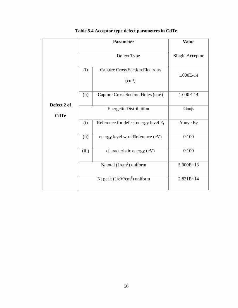
56
Table 5.4 Acceptor type defect parameters in CdTe
Defect 2 of
CdTe
Parameter Value
Defect Type Single Acceptor
(i) Capture Cross Section Electrons
(cm²)
1.000E-14
(ii) Capture Cross Section Holes (cm²) 1.000E-14
Energetic Distribution Gauβ
(i) Reference for defect energy level Et Above EV
(ii) energy level w.r.t Reference (eV) 0.100
(iii) characteristic energy (eV) 0.100
Nt total (1/cm3) uniform 5.000E+13
Nt peak (1/eV/cm3) uniform 2.821E+14

57
Table 5.5 CdTe / CdS Interface parameters
CdTe / CdS
Interface
Parameter Value
Defect Type Acceptor
(i) Capture Cross Section Electrons (cm²) 5.00E-16
(ii) Capture Cross Section Holes (cm²) 5.00E-16
Energetic Distribution Gauβ
(i) Reference for defect energy level Et Above middle of
interface gap
(ii) energy level w.r.t Reference (eV) 0.600
(iii) characteristic energy (eV) 0.100
Nt total (1/cm3) uniform 1.00E+10
Nt peak (1/eV/cm3) uniform 5.64E+10
Allow Tunneling to Interface States
(i) Relative mass of electrons 2.000E-1
(ii) Relative mass of holes 8.000E-1

58
Table 5.6 CdS material properties
CdS
Nanowires
Parameter Value
Thickness (μm) 0.200
Bandgap (eV) 3.200
Electron Affinity (eV) 4.100
Dielectric Permittivity (relative) 9.000
CB Effective Density of States (1/cm3) 2.300E+18
VB Effective Density of States (1/cm3) 1.700E+19
Electron Thermal Velocity (cm/s) 1.000E+7
Hole Thermal Velocity (cm/s) 1.000E+7
Electron Mobility (cm²/Vs) 1.000E+2
Hole Mobility (cm²/Vs) 2.500E+1
Allow tunneling
(i) Effective mass of electrons 2.000E-1
(ii) Effective mass of holes 8.000E-1
Shallow Uniform Donor Density ND (1/cm3) 1.000E+18

59
Table 5.7 Acceptor type defect parameters in CdS
Defect 1 of CdS
Parameter Value
Defect Type Single Acceptor
(i) Capture Cross Section Electrons
(cm²)
1.000E-14
(ii) Capture Cross Section Holes (cm²) 1.000E-14
Energetic Distribution Single
(i) Reference for defect energy level Et Above Ei
(ii) energy level w.r.t Reference (eV) 0.000
Nt total (1/cm3) uniform 1.000E+16

60
Table 5.8 SnO2 material properties
SnO2
Parameter Value
Thickness (μm) 0.100
Bandgap (eV) 3.600
Electron Affinity (eV) 4.500
Dielectric Permittivity (relative) 9.000
CB Effective Density of States (1/cm3) 3.200E+18
VB Effective Density of States (1/cm3) 2.500E+19
Electron Thermal Velocity (cm/s) 1.000E+7
Hole Thermal Velocity (cm/s) 1.000E+7
Electron Mobility (cm²/Vs) 1.000E+2
Hole Mobility (cm²/Vs) 2.500E+1
Shallow Uniform Donor Density ND (1/cm3) 1.000E+18

61
Table 5.9 Neutral type defect parameters in SnO2
Defect 1 of SnO2
Parameter Value
Defect Type Neutral
(i) Capture Cross Section Electrons (cm²) 1.000E-15
(ii) Capture Cross Section Holes (cm²) 1.000E-13
Energetic Distribution Gauβ
(i) Reference for defect energy level Et Above Ei
(ii) energy level w.r.t Reference (eV) 0.000
(iii) characteristic energy (eV) 0.100
Nt total (1/cm3) uniform 1.000E+15
Nt peak (1/eV/cm3) uniform 5.642E+15

62
Table 5.10 FTO material properties
FTO
Parameter Value
Thickness (μm) 0.300
Bandgap (eV) 3.600
Electron Affinity (eV) 4.800
Dielectric Permittivity (relative) 9.000
CB Effective Density of States (1/cm3) 3.200E+18
VB Effective Density of States (1/cm3) 2.500E+19
Electron Thermal Velocity (cm/s) 1.000E+7
Hole Thermal Velocity (cm/s) 1.000E+7
Electron Mobility (cm²/Vs) 3.000E+1
Hole Mobility (cm²/Vs) 7.500E+0
Shallow Uniform Donor Density ND (1/cm3) 5.000E+20

63
Table 5.11 Neutral type defect parameters in FTO
Defect 1 of FTO
Parameter Value
Defect Type Neutral
(i) Capture Cross Section Electrons (cm²) 1.000E-15
(ii) Capture Cross Section Holes (cm²) 1.000E-12
Energetic Distribution Gauβ
(i) Reference for defect energy level Et Above Ei
(ii) energy level w.r.t Reference (eV) 0.000
(iii) characteristic energy (eV) 0.100
Nt total (1/cm3) uniform 1.000E+15
Nt peak (1/eV/cm3) uniform 5.642E+15
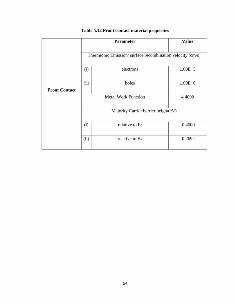
64
Table 5.12 Front contact material properties
Front Contact
Parameter Value
Thermionic Emission/ surface recombination velocity (cm/s)
(i) electrons 1.00E+5
(ii) holes 1.00E+6
Metal Work Function 4.4000
Majority Carrier barrier height(eV)
(i) relative to Ef -0.4000
(ii) relative to Ev -0.2692

65
Figure 5.10 SCAPS: I-V Panel
Figure 5.10 shows the results of the Simulated J-V characteristics at 300 K for the
parameters shown in Table 5.1 – 5.12. in SCAPS

66
CHAPTER 6. RESULTS AND DISCUSSION
Experimental results on the fabrication of titanium oxide nanotubes and the spectral
absorption of thin film CdS and CdS nanopillars are presented in Section 6.1 while the
Section 6.2 describes the results of numerical calculations and the related discussion.
6.1 Nano porous Titania Template: Experimental results
For our experiments, a nano porous template made of titanium dioxide (titania)
serves as the host for embedding the CdS nanopillars inside its nanopores. The nanoporous
titania matrix, by itself has negligible absorption in the visible part of the spectrum, and
the Titania-CdS combination is advantageous over the traditional CdS window layer
because it enhances the optical transmission through the window layer by increasing the
effective energy band gap of CdS and thus extending the transmission edge of CdS.
In order to investigate the effect of host nanotube parameters, a study was done on
the parameters that affect the pore diameter and the pitch of Titania nanotube arrays. Nano
porous Titania templates were fabricated to study the effect of some of the parameters that
affect the pore diameter and the pitch of the nanotube arrays. The results on the effect of
anodization voltage and fluoride ion concentration in the anodization solution on the pore
diameter and the pitch for the experimentally fabricated devices will be discussed below
with the help of Table 6.1 and Figures 6.1-6.6.

67
Table 6.1 Effect of fluoride ion concentration and anodization voltage on pore
diameter and interpore distance
Sample # NH4F
Anodization
Voltage
Average Pore
Diameter
Average interpore
distance
1 2 mL 50 V 58.3 nm 85.4 nm
2 2 mL 60 V 50 nm 81.8 nm
3 0.81 mL 50 V 57.5 nm 88.2 nm
4 0.3 mL 40 V 49.3 nm ---
5 0.3 mL 50 V 57 nm 88.6 nm
6 0.3 mL 60 V 42 nm 79.2 nm
Table 6.1 shows the effect of fluoride ion concentration and anodization voltage on pore
diameter and interpore distance (center-to-center distance between two adjoining
nanopores). Three different fluoride ion concentration and three different anodization
voltages were used, to successfully fabricate nano porous Titania template, in order to study
their effect on the pore diameter and the pitch.

68
Figure 6.1 Top view SEM image of Sample # 1 fabricated in a fresh electrolyte
comprising of 98 mL of EG and 2 mL of NH4F at an anodization voltage of 50 V.
Figure 6.1 shows the top view SEM image of nanoporous template fabricated in a
fresh electrolyte comprising of 98 mL of EG (Ethylene Glycol ) and 2 mL of NH4F at an
anodization voltage of 50 V, the average pore diameter of the nanotubes thus obtained was
found to be 58.5 nm and an average interpore distance of 85.4 nm.

69
Figure 6.2 Top view SEM image of sample # 2 fabricated in a fresh electrolyte
comprising of 98 mL of EG and 2 mL of NH4F at an anodization voltage of 60 V.
Figure 6.2 shows the top view SEM image of nanoporous template fabricated in a
fresh electrolyte comprising of 98 mL of EG (Ethylene Glycol ) and 2 mL of NH4F at an
anodization voltage of 60 V, the average pore diameter of the nanotubes thus obtained was
found to be 50 nm and an average interpore distance of 81.8 nm.
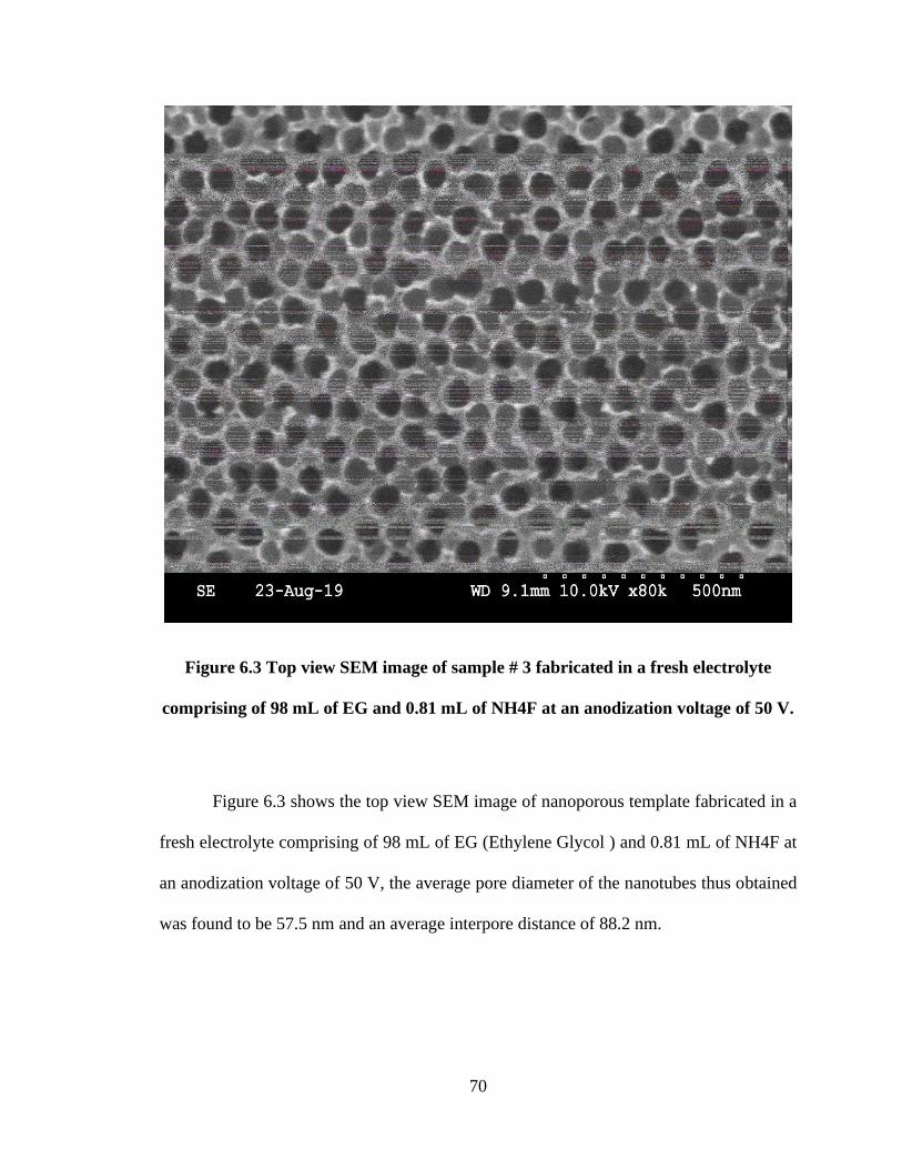
70
Figure 6.3 Top view SEM image of sample # 3 fabricated in a fresh electrolyte
comprising of 98 mL of EG and 0.81 mL of NH4F at an anodization voltage of 50 V.
Figure 6.3 shows the top view SEM image of nanoporous template fabricated in a
fresh electrolyte comprising of 98 mL of EG (Ethylene Glycol ) and 0.81 mL of NH4F at
an anodization voltage of 50 V, the average pore diameter of the nanotubes thus obtained
was found to be 57.5 nm and an average interpore distance of 88.2 nm.
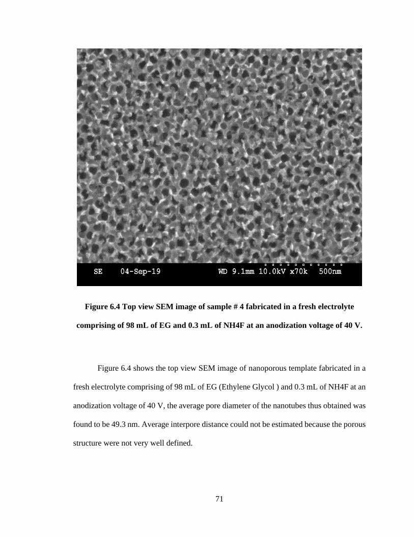
71
Figure 6.4 Top view SEM image of sample # 4 fabricated in a fresh electrolyte
comprising of 98 mL of EG and 0.3 mL of NH4F at an anodization voltage of 40 V.
Figure 6.4 shows the top view SEM image of nanoporous template fabricated in a
fresh electrolyte comprising of 98 mL of EG (Ethylene Glycol ) and 0.3 mL of NH4F at an
anodization voltage of 40 V, the average pore diameter of the nanotubes thus obtained was
found to be 49.3 nm. Average interpore distance could not be estimated because the porous
structure were not very well defined.

72
Figure 6.5 Top view SEM image of sample # 5 fabricated in a fresh electrolyte
comprising of 98 mL of EG and 0.3 mL of NH4F at an anodization voltage of 50 V.
Figure 6.5 shows the top view SEM image of nanoporous template fabricated in a
fresh electrolyte comprising of 98 mL of EG (Ethylene Glycol ) and 0.3 mL of NH4F at an
anodization voltage of 50 V, the average pore diameter of the nanotubes thus obtained was
found to be 57 nm and an average interpore distance of 88.2 nm.
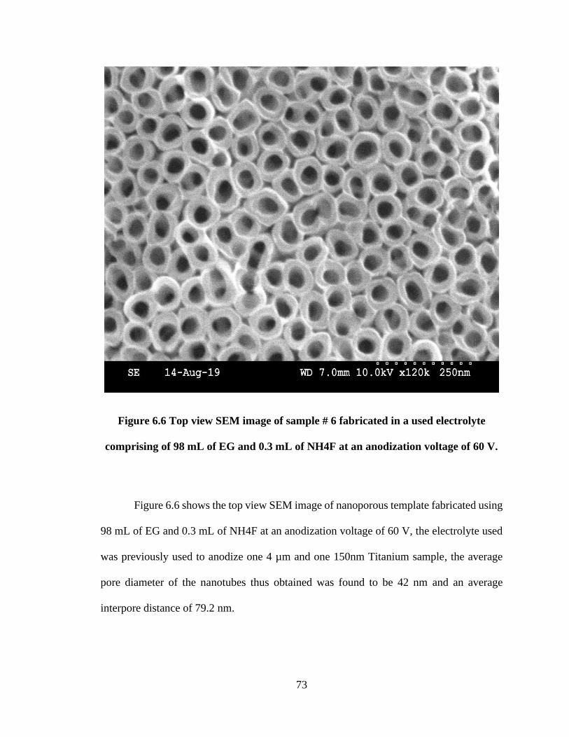
73
Figure 6.6 Top view SEM image of sample # 6 fabricated in a used electrolyte
comprising of 98 mL of EG and 0.3 mL of NH4F at an anodization voltage of 60 V.
Figure 6.6 shows the top view SEM image of nanoporous template fabricated using
98 mL of EG and 0.3 mL of NH4F at an anodization voltage of 60 V, the electrolyte used
was previously used to anodize one 4 µm and one 150nm Titanium sample, the average
pore diameter of the nanotubes thus obtained was found to be 42 nm and an average
interpore distance of 79.2 nm.

74
6.1.1.1 Effect of Fluoride ion concentration on pore diameter
Three samples (Sample # 1, Sample # 3 and sample # 5) were anodized at 50 V
with varying concentration of fluoride ions in the electrolyte. These samples were anodized
in electrolyte containing 2 mL, 0.81 mL and 0.3 mL of Nh4F for Sample # 1, Sample # 3
and sample # 5 respectively. The anodization was otherwise performed under similar
anodization conditions except for varying the fluoride ion concentration. From the Table
6.1 and Figure 1, 3, and 5 it is seen that the pore diameter increases only slightly, from 57
nm to 58.3 nm , when the fluoride concentration is increased from 0.3 mL to 2 mL It is
clear that in the experimental range investigated here, pore diameter of the titania nanotube
matrix is rather insensitive to the ammonium fluoride concentration.
6.1.1.2 Effect of anodization voltage on pore diameter
In literature various authors have different opinion on the effect of anodization
voltage on the pore diameter. In Ethylene Glycol based electrolyte several authors have
suggested that the pore diameter increases with the increase in anodization voltage
[28,29,41,47,56,57]. However, Y. Alivov et al. reported that in glycerol-based electrolyte
the anodization potential does not have any clear dependence on the pore diameter of the
TiO2 nanotubes, when the anodization voltage was varied over the range of 10-240V [42].
For our devices, the effect of anodization voltage on pore diameter can be seen from
the results obtained from sample # 4, sample # 5 and sample # 6. The electrolyte contained
0.3 mL of NH4F in 98 mL of Ethylene Glycol. Sample # 4, sample # 5 and sample # 6 were
anodized at three different voltages of 40 V, 50 V and 60 V respectively. From Table 6.1
and Figures 4-6 it is seen that when the anodization voltage is increased from 40 V to 50

75
V, the pore diameter increases from 49.3 nm to 57 nm. However, when the anodization
voltage is increased further form 50 V to 60 V, the pore diameter decreased from 57 nm to
42 nm. Thus, for the case of ethylene glycol based electrolyte it can be suggested that there
is an optimum anodization voltage at which the pore diameter is maximum for a fixed
flouride ion concentration.
6.1.1.3 Effect of Fluoride ion concentration on the pitch
The effect of fluoride ion concentration on the pitch can be seen with two sets of
samples anodized at two different voltages. Set one contained Sample # 1, Sample # 3 and
sample # 5 anodized at 50 V where the NH4F content in the electrolyte were 2 mL, 0.81
mL and 0.3 mL respectively. Set two consisted of Sample # 2 and Sample # 6 anodized at
60 V. In set 1, pitch decreased from 88.6 nm to 85.4 nm when the Ammonium Fluoride
content was increased from 0.3 mL to 2 ml. In set 2, pitch increased slightly from 79.2 nm
to 81.8 nm when the Ammonium Fluoride content was increased from 0.3 mL to 2 ml. It
is clear that in the experimental range investigated here, the pitch (interpore distance) of
the titania nanotube matrix is rather insensitive to the ammonium fluoride concentration.
6.1.1.4 Effect of anodization voltage on pitch
The effect of anodization voltage on the pitch can be seen with two sets of samples
anodized at two different voltages. Set one contained Sample # 1 and sample # 2 anodized
at 50 V and 60 V respectively, where the electrolyte contained 2 mL of NH4F in 98 mL of
Ethylene Glycol. Set two consisted of Sample # 5 and Sample # 6 anodized at 50 V and 60

76
V respectively, where the electrolyte content was 0.3 mL of NH4F in 98 mL of Ethylene
Glycol. In set 1, pitch decreased from 85.4 nm to 81.8 nm when the anodization voltage
was increased from 50 V to 60 V. In set 2, pitch decreased from 88.6 nm to 79.2 nm when
the anodization voltage was increased from 50 V to 60 V. It is clear that an increase in
anodization voltage from 50 V to 60 V leads to a substantial reduction in the pitch of the
titania nanotube matrix.
From the above discussion it can be concluded that the anodization voltage is the more
effective parameter, which can be tailored and optimized to fabricate Titania Nanotube
arrays of desired porosity.

77
6.2 Numerical Results and Discussion
6.2.1 Interpolation of absorption profile for various CdS coverages
TiO2 nanotubes, Planar CdS and Nanowire CdS were fabricated as explained in
Chapter 3 and their absorption spectra were measured using Cary 50 UV-Vis
Spectrophotometer. Defining the “CdS coverage” (x) as the fraction of the total surface
area filled by the embedded CdS nanopillars, the absorption spectrum (A) for a particular
value of CdS coverage (x) was obtained by interpolation as expressed in the Equation 6.1
below,
(𝑥) ∗ 𝐴𝐶𝑑𝑆 𝑃𝑙𝑎𝑛𝑎𝑟 + (1 − 𝑥) ∗ 𝐴𝑇𝑖𝑂2= 𝐴𝐶𝑑𝑆 𝑁𝑎𝑛𝑜𝑤𝑖𝑟𝑒 (𝑥) (6.1)
300 400 500 600 700 800
0.0
0.1
0.2
0.3
0.4
0.5
Absorption vs Wavelength for 32% CdS Coverage
Experimental vs Theoretical
Wavelength (nm)
Ab
so
rpti
on
(A
u) 32% CdS Coverage - Theoretical
32% CdS Coverage - Experimental
Figure 6.7 Absorption vs Wavelength for 32% CdS Coverage Experimental vs
Theoretical

78
Figure 6.7 shows the comparison between the absorption profile for experimentally
fabricated CdS Nanowires and the theoretical absorption profile CdS Nanowires for 32%
coverage. The theoretical absorption profile was interpolated using equation (6.1). It is
seen that the theoretical absorption profile for CdS Nanowires follows closely the
experimental profile thus verifying that the linear assumption used in equation (6.1)
holds.
The absorption profiles interpolated using equation (6.1) was input in SCAPS to
replace the default absorption profile for different coverages of CdS.
300 400 500 600 700 800
0.0
0.2
0.4
0.6
0.8
Absorption vs Wavelength for 80%-100% CdS
Wavelength (nm)
Ab
so
rpti
on
(A
u)
Planar
95% CdS
90% CdS
85% CdS
80% CdS
Figure 6.8 Theoretical absorption profile CdS Nanowires for 80% - 100% coverage

79
300 400 500 600 700 800
0.0
0.2
0.4
0.6
0.8
Absorption vs Wavelength for 55%-75% CdS
Wavelength (nm)
Ab
so
rpti
on
(A
u)
75% CdS
70% CdS
65% CdS
60% CdS
55% CdS
Figure 6.9 Theoretical absorption profile CdS Nanowires for 55% - 75% coverage
300 400 500 600 700 800
0.0
0.2
0.4
0.6
Absorption vs Wavelength for 30%-50% CdS
Wavelength (nm)
Ab
so
rpti
on
(A
u)
50% CdS
45% CdS
40% CdS
35% CdS
32% CdS
30% CdS
Figure 6.10 Theoretical absorption profile CdS Nanowires for 30% - 50% coverage

80
300 400 500 600 700 800
0.0
0.1
0.2
0.3
0.4
Absorption vs Wavelength for 5%-25% CdS
Wavelength (nm)
Ab
so
rpti
on
(A
u)
25% CdS
20% CdS
15% CdS
10% CdS
5% CdS
Figure 6.11 Theoretical absorption profile CdS Nanowires for 5% - 25% coverage
Figures 6.8 – 6.11 shows the theoretical absorption profile CdS Nanowires for 5% -100%
coverage. The absorption spectrum (A) for a particular value of CdS coverage (x) was
obtained by interpolation as expressed in the Equation 6.1. From the figures 6.8 –6.11 it
can be seen that the absorption in the lower wavelength region drops from ≈0.8 Au to
≈0.25 Au when the CdS coverage drops from 100% to 5%.
The total interface state density (integrated over all energies) for the CdTe / CdS
interface was varied in the range of 1.50E+4 (cm-2) to 3.00E+10 (cm-2) for different CdS
coverages (0.0001% CdS to 100% CdS) to account for the reduced interface area (to
fraction x) at the junction between the nanowire CdS window layer and the absorber CdTe
layer. Acceptor type defect with Gauβ type of Energetic Distribution was considered for
the CdTe / CdS interface.

81
As the interface area between the CdTe / CdS junction reduces (from 100% CdS to
0.0001% CdS), a reduction in dark saturation current is obtained due to the decrease in
interface recombination velocity that allows for less recombination at the interface which
in turn enhances the overall device performance.
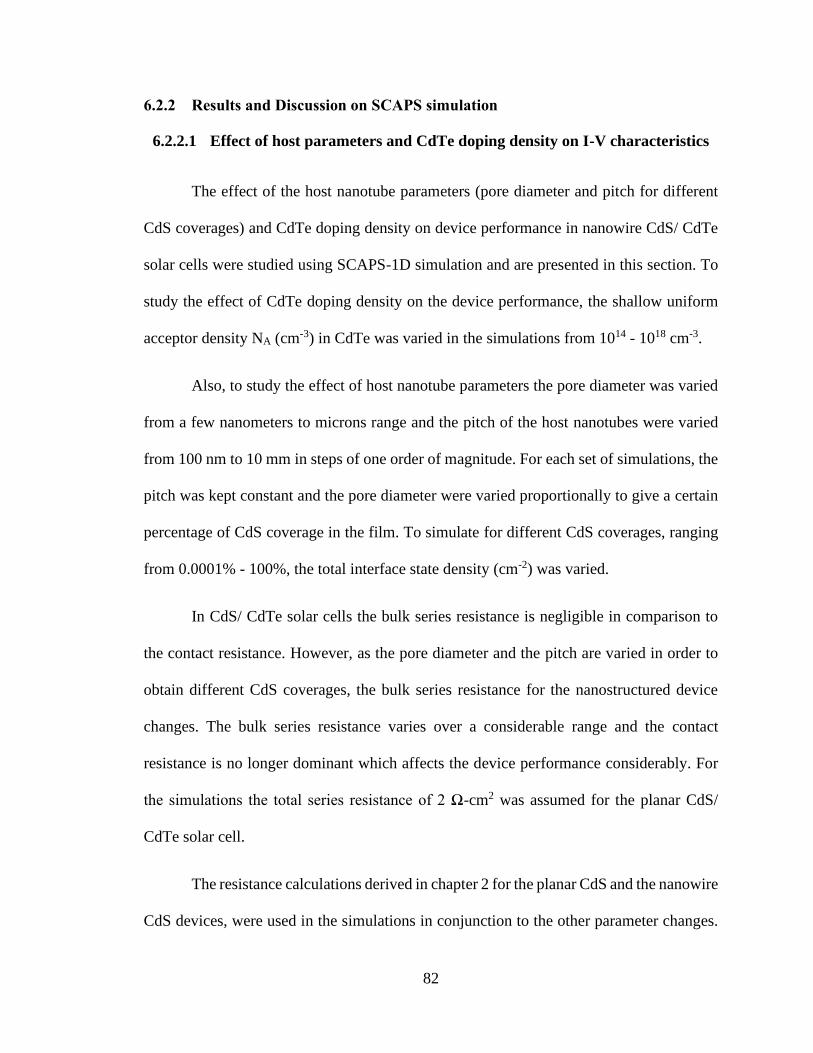
82
6.2.2 Results and Discussion on SCAPS simulation
6.2.2.1 Effect of host parameters and CdTe doping density on I-V characteristics
The effect of the host nanotube parameters (pore diameter and pitch for different
CdS coverages) and CdTe doping density on device performance in nanowire CdS/ CdTe
solar cells were studied using SCAPS-1D simulation and are presented in this section. To
study the effect of CdTe doping density on the device performance, the shallow uniform
acceptor density NA (cm-3) in CdTe was varied in the simulations from 1014 - 1018 cm-3.
Also, to study the effect of host nanotube parameters the pore diameter was varied
from a few nanometers to microns range and the pitch of the host nanotubes were varied
from 100 nm to 10 mm in steps of one order of magnitude. For each set of simulations, the
pitch was kept constant and the pore diameter were varied proportionally to give a certain
percentage of CdS coverage in the film. To simulate for different CdS coverages, ranging
from 0.0001% - 100%, the total interface state density (cm-2) was varied.
In CdS/ CdTe solar cells the bulk series resistance is negligible in comparison to
the contact resistance. However, as the pore diameter and the pitch are varied in order to
obtain different CdS coverages, the bulk series resistance for the nanostructured device
changes. The bulk series resistance varies over a considerable range and the contact
resistance is no longer dominant which affects the device performance considerably. For
the simulations the total series resistance of 2 Ω-cm2 was assumed for the planar CdS/
CdTe solar cell.
The resistance calculations derived in chapter 2 for the planar CdS and the nanowire
CdS devices, were used in the simulations in conjunction to the other parameter changes.

83
From the equations 2.29 and 2.37, it is seen that the bulk series resistance in case of
planar devices is inversely proportional to the doping. In case of nanowire devices, the
bulk series resistance is dependent on the doping, the pore diameter, pitch and the CdTe
thickness. However, for the simulations the CdTe thickness was kept constant at 5 μm.
𝑹𝒆𝒇𝒇 𝑷𝒍𝒂𝒏𝒂𝒓 =𝜼𝑵𝟏𝜶
𝑰𝑳𝝁𝒑𝒑𝑨[𝒕𝒆−𝜶𝒕
𝜶−
𝒆−𝜶𝒕
𝜶𝟐+
𝟏
𝜶𝟐]
(2.29)
𝑹𝒆𝒇𝒇 𝒏𝒂𝒏𝒐𝒘𝒊𝒓𝒆 = 𝑹𝒆𝒇𝒇 𝑷𝒍𝒂𝒏𝒂𝒓 ∗ [𝟏 + (𝑳
√𝟐−
𝑫
𝟐) ∗
𝟏
𝒉]
(2.37)
The results of the simulations showed that by using CdS nanopillars embedded in
nanoporous template as the window layer, an absolute gain of 1.05% in efficiency could
be achieved over the case of the planar CdS window layer. This gain in efficiency was
obtained when the CdS coverage was 0.1%, CdTe doping density was 1017 cm-3, the pore
diameter could range from 2.35nm – 23.48nm and the interpore distance ranging from
100nm – 1000nm. The planar device was 24.88% efficient whereas 25.93% efficient solar
cells could be achieved with the CdS nanopillars device.
In the sections to follow the results obtained from SCAPS simulations for an
interpore distance of 100nm will be discussed and comparison will be made on the solar
cell parameters, Voc, Jsc, FF and Efficiency, for various CdTe dopings against optimal
doping of 1017 cm-3. The results obtained for an interpore distance of 100nm is chosen over
an interpore distance of 1000nm as the nanoporous Titania template fabricated in our lab
is closer to 100nm. Other results obtained from the SCAPS simulation to study the effect
of various parameter are presented as plots and tables in the Appendix section.

84
6.2.2.2 Short Circuit Current enhancement
The bandgap of planar Cadmium Sulfide is 2.4 eV, loss of photocurrent is caused
by light absorption in the n-Cadmium Sulfide (CdS) window layer in the shorter
wavelength region (below 512 nm), leading to the degradation of cell performance. High
density of recombination sites present in CdS films prevents the photons, with wavelength
less than 512 nm that are absorbed in CdS, from contributing to the collected photocurrent.
This loss is reduced when an array of CdS nanowires replaces the conventional planar n-
CdS film.
When the CdS nanowires are embedded in the nano porous template, an increase
in the effective bandgap for CdS is obtained which in turn suppresses the photon loss in
the lower wavelength region and makes the window layer more transmittive to sunlight
than is the case with the traditional planar CdS window layer. This leads to an increase in
the number of photons available to the p-CdTe absorber. These extra photons lead to an
increase the short circuit current. Also, the dominant junction current mechanism at the
nanowire CdS-CdTe heterojunction involves interface recombination at the CdS-CdTe
interface [58]. This interface recombination current is reduced in the case of the CdS-
nanopillars-window layer and therefore a higher open circuit voltage (Voc) is achieved.

85
1 2 3 4 5
27.8
27.9
28.0
28.1
28.2
28.3
28.4
20 40 60 80 100
Jsc vs % CdS Coverage 1-100%, L = 100 nm
%CdS Coverage
Js
c(m
A/c
m2)
Doping 1014
Doping 1015
Doping 1016
Doping 1017
Doping 1018
Figure 6.12 Jsc vs 1-100% CdS Coverage Interpore Distance 100nm
Figure 6.12 shows the plot of short circuit current vs CdS coverage for the simulated results
where the CdS coverage was varied from 1% to 100% for various doping levels. The CdTe
doping density varied from 1014 cm-3 to 1018 cm-3.
It is seen that as a result of transmission gain obtained using nanopillars of CdS, the
short circuit current increases with a decrease in the CdS coverage. An increase in short
circuit current was expected as the number of photons available to the p-CdTe absorber
increased by lowering the CdS coverage, i.e., a smaller number of photons being lost in the
lower wavelength region for the nanowire CdS as compared to the planar CdS. At relatively
low doping levels, 1014 cm-3 to 1017 cm-3, the transmission gain is dominant and results in
a better enhancement of the short circuit current.

86
At higher doping levels the dopants, impurities that also act as recombination
centers, has more pronounced effect on the short circuit current. The absolute gain in the
short circuit current at higher doping level gets reduced as was expected, an increase in the
number of recombination sites counters the gain that was obtained from higher
transmission using nanostructures. However, at the doping level of 1017 cm-3 transmission
gain still being the dominant mechanism results in an increase in the short circuit current,
as the number of recombination sites are not enough to counter the gain obtained from
transmission.
At higher doping level of 1018 cm-3 the dopants (a) offers low resistivity, higher
mobility for the flow of electrons and holes; (b) act as recombination centers causing
greater recombination. However, the recombination tends to be more dominant mechanism
and despite of the higher mobility the electrons and holes generated by the photons
absorbed in CdTe layer, all the electrons and holes generated do not reach the junction.
This causes a loss in photocurrent; this effect is seen in figure 6.12 where we see that there
is a slight dip in the short circuit current with the decreasing CdS coverage.
The maximum short circuit current of 28.3 mA cm-2 is obtained for doping density
of 1017 cm-3.

87
0.00001 0.0001 0.001 0.01 0.1 1
28.10
28.15
28.20
28.25
28.30
28.35
Jsc vs % CdS Coverage 0.0001-0.1%, L = 100 nm
%CdS Coverage
Js
c(m
A/c
m2)
Doping 1014
Doping 1015
Doping 1016
Doping 1017
Doping 1018
Figure 6.13 Jsc vs 0.0001-0.1% CdS Coverage Interpore Distance 100nm
Figure 6.13 shows the plot of short circuit current vs CdS coverage for the simulated results
where the CdS coverage was varied from 0.0001% to 0.1% for various doping levels. The
CdTe doping density varied from 1014 cm-3 to 1018 cm-3.
In the plot it is seen that the short circuit current, irrespective of the doping level,
saturates below 0.1% CdS coverage. This gives us the threshold point below which the
there is no additional advantage to be gained in terms of transmission.
The maximum short circuit current of 28.3 mA cm-2, after which it saturates, is
obtained for doping density of 1017 cm-3.

88
6.2.2.3 Enhancement in the Open Circuit Voltage
The dominant junction current mechanism at the nanowire CdS-CdTe
heterojunction involves interface recombination at the CdS-CdTe interface [58]. Reduction
in the junction area between CdS and CdTe leads to a reduction in the total number of
interface states. This is an advantage because interface states are known [59,60] to lead an
increase in the effective reverse saturation current and a reduced open circuit voltage.
As the interface area at the junction between CdTe and CdS nanowires for different
CdS coverage is reduced by a factor of x. Assuming 𝐼01 =1
𝑥𝐼02 and 𝐼𝐿2 = 𝑦 ∗ 𝐼𝐿1
Where y represents the current enhancement factor due to a better window layer as has
been demonstrated in Figures 6.12 and 6.13 and I0 and IL are the effective reverse
saturation current and the light generated current respectively.
𝑉𝑂𝐶 =𝜂𝑘𝑇
𝑞ln (
𝐽𝑆𝐶
𝐽0+ 1) (2.16)
For Planar CdS/ CdTe Solar Cell:
𝑉𝑂𝐶_𝑃𝑙𝑎𝑛𝑎𝑟 = 𝜂𝑘𝑇
𝑞𝐿𝑛 (
𝐼𝐿1
𝐼01) (6.2)
For Nanowire CdS/ CdTe Solar Cell:
𝑉𝑂𝐶_𝑁𝑎𝑛𝑜𝑤𝑖𝑟𝑒 = 𝜂𝑘𝑇
𝑞𝐿𝑛 (
𝐼𝐿2
𝐼02) (6.3)

89
Therefore,
𝑉𝑂𝐶_𝑁𝑎𝑛𝑜𝑤𝑖𝑟𝑒 − 𝑉𝑂𝐶_𝑃𝑙𝑎𝑛𝑎𝑟 = 𝜂𝑘𝑇
𝑞𝐿𝑛 (
𝐼𝐿2/𝐼𝐿1
𝐼01/𝐼02) (6.4)
From the above equation 6.4 it is seen that the open circuit voltage can be enhanced by
using nanowire CdS window layer. The open circuit voltage depends on the reverse
saturation current density, which in turn depends on the acceptor doping density.
𝐽0 = 𝑞𝑁𝐶𝑁𝑉 (1
𝑁𝐴√
𝐷𝑛
𝜏𝑛+
1
𝑁𝐷√
𝐷𝑝
𝜏𝑝) 𝑒−
𝐸𝑔
𝑘𝑇 (2.17)
From equations (6.4) & (2.17) it is seen that with an increase in the doping concentration
the effective reverse saturation current decreases leading to an increase in the open
circuit voltage.
The reverse saturation current across the junction in CdS/ CdTe solar cell is
comprised of (i) diffusion current, (ii) generation-recombination current, (iii) tunneling
between CdS conduction band and empty trap levels followed by the hole capture by the
trap and (iv) recombination via interface states [60]. The dominant junction current
mechanism at the nanowire CdS-CdTe heterojunction involves interface recombination at
the CdS-CdTe interface [58].
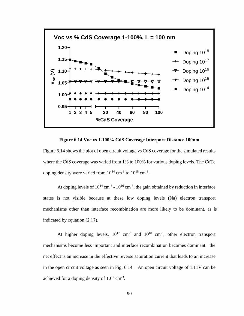
90
1 2 3 4 5
0.95
1.00
1.05
1.10
1.15
1.20
20 40 60 80 100
Voc vs % CdS Coverage 1-100%, L = 100 nm
%CdS Coverage
Vo
c (
V)
Doping 1014
Doping 1015
Doping 1016
Doping 1017
Doping 1018
Figure 6.14 Voc vs 1-100% CdS Coverage Interpore Distance 100nm
Figure 6.14 shows the plot of open circuit voltage vs CdS coverage for the simulated results
where the CdS coverage was varied from 1% to 100% for various doping levels. The CdTe
doping density were varied from 1014 cm-3 to 1018 cm-3.
At doping levels of 1014 cm-3 - 1016 cm-3, the gain obtained by reduction in interface
states is not visible because at these low doping levels (Na) electron transport
mechanisms other than interface recombination are more likely to be dominant, as is
indicated by equation (2.17).
At higher doping levels, 1017 cm-3 and 1018 cm-3, other electron transport
mechanisms become less important and interface recombination becomes dominant. the
net effect is an increase in the effective reverse saturation current that leads to an increase
in the open circuit voltage as seen in Fig. 6.14. An open circuit voltage of 1.11V can be
achieved for a doping density of 1017 cm-3.

91
0.00001 0.0001 0.001 0.01 0.1 1
0.95
1.00
1.05
1.10
1.15
1.20
Voc vs % CdS Coverage 0.0001-0.1%, L = 100 nm
%CdS Coverage
Vo
c (
V)
Doping 1014
Doping 1015
Doping 1016
Doping 1017
Doping 1018
Figure 6.15 Voc vs 0.0001-0.1% CdS Coverage Interpore Distance 100nm
Figure 6.15 shows the plot of open circuit voltage vs CdS coverage for the simulated
results where the CdS coverage was varied from 0.0001% to 0.1% for various doping
levels. The CdTe doping density were varied from 1014 cm-3 to 1018 cm-3.
The dominant junction current mechanism at the nanowire CdS-CdTe
heterojunction involves interface recombination at the CdS-CdTe interface [58]. The open
circuit voltage increases as the CdTe doping is increased, increase in the doping level
causes a reduction in the effective reverse saturation current. However, the number of
interface states below 0.1% CdS coverage becomes so low such that the recombination via
interface states in no longer the dominant junction current mechanism and any further
reduction in the CdS coverage does not improve the Voc any further.
An open circuit voltage of 1.153V can be achieved for a doping density of 1018 cm-3.

92
6.2.2.4 Effect of decreasing CdS coverage on Fill Factor
When the parasitic series resistance and shunt resistance, 𝑅𝑠 and 𝑅𝑠ℎ, both have
negligible effect on the solar cell performance, the fill factor can be approximately
expressed in terms of open-circuit voltage as [18]
𝐹𝐹 =
𝑞𝑉𝑂𝐶
𝑘𝑇− 𝑙𝑛 (0.72 +
𝑞𝑉𝑂𝐶
𝑘𝑇)
1 +𝑞𝑉𝑂𝐶
𝑘𝑇
(2.19)
However, when either the series resistance or the shunt resistance has significant
effect on the device performance the above equation may yield inaccurate results.

93
1 2 3 4 5
76
78
80
82
84
20 40 60 80 100
FF vs % CdS Coverage 1-100%, L = 100 nm
%CdS Coverage
Fill
Fa
cto
r (%
)
Doping 1014
Doping 1015
Doping 1016
Doping 1017
Doping 1018
Figure 6.16 FF vs 1-100% CdS Coverage Interpore Distance 100nm
Figure 6.16 shows the plot of fill factor vs CdS coverage for the simulated results where
the CdS coverage was varied from 1% to 100% for various doping levels. The CdTe doping
density were varied from 1014 cm-3 to 1018 cm-3.
At lower acceptor doping density of 1014 cm-3 the bulk series resistance is high that
counters the effect of increase in Voc as the interface state density is reduced. The overall
effect is such that the fill factor of the device practically remains unchanged.
However, at higher acceptor doping density of 1017 cm-3 the bulk series resistance
is lower and the dominant factor causing the increase in fill factor is the contribution from
increase in Voc with reduced number of interface states. The fill factor gradually increases
in a linear fashion with the decreasing CdS coverage. At even higher acceptor doping
density of 1018 cm-3, the series resistance has negligible effect to counter the gain obtained

94
from the increase in Voc. This can be seen in figure 6.16, where, the fill factor increases
exponentially with decreasing CdS coverage.
0.00001 0.0001 0.001 0.01 0.1 1
76
78
80
82
84
FF vs % CdS Coverage 0.0001-0.1%, L = 100 nm
%CdS Coverage
Fill
Fa
cto
r (%
)
Doping 1014
Doping 1015
Doping 1016
Doping 1017
Doping 1018
Figure 6.17 FF vs 0.0001-0.1% CdS Coverage Interpore Distance 100nm
Figure 6.17 shows the plot of fill factor vs CdS coverage for the simulated results
where the CdS coverage was varied from 0.0001% to 0.1% for various doping levels.
The CdTe doping density were varied from 1014 cm-3 to 1018 cm-3.
The fill factor tracks the open circuit voltage when the parasitic series resistance
and shunt resistance, 𝑅𝑠 and 𝑅𝑠ℎ, both have negligible effect on the solar cell performance.
As the open circuit voltage reaches the saturation at less than 0.1% CdS coverage results
in the saturation of the fill factor below 0.1% CdS coverage, the bulk series resistance is
negligibly affected for a interpore distance of 100 nm.

95
6.2.2.5 Effect of decreasing CdS coverage on Efficiency
𝑃𝐶𝐸 (𝜂) =𝑃𝑚(𝑀𝑎𝑥𝑖𝑚𝑢𝑚 𝑃𝑜𝑤𝑒𝑟 𝑡ℎ𝑎𝑡 𝑡ℎ𝑒 𝑠𝑜𝑙𝑎𝑟 𝑐𝑒𝑙𝑙 𝑐𝑎𝑛 𝑑𝑒𝑙𝑖𝑣𝑒𝑟)
𝐼𝑛𝑐𝑖𝑑𝑒𝑛𝑡 𝑃𝑜𝑤𝑒𝑟 𝑓𝑟𝑜𝑚 𝑆𝑢𝑛𝑙𝑖𝑔ℎ𝑡
=𝑉𝑂𝐶 ∗ 𝐼𝑆𝐶 ∗ 𝐹𝐹
𝑃𝑖𝑛𝑐
(2.21)
Where 𝑃𝑖𝑛𝑐 is the incident power from the incoming solar radiation and is given by
𝑃𝑖𝑛𝑐 = 𝐴 ∫ 𝐹(𝜆) (ℎ𝑐
𝜆)
∞
0
𝑑𝜆 (2.22)
A is the total device area, 𝐹(𝜆) is the incident photon flux and (ℎ𝑐
𝜆) is the energy associated
with each photon.
The efficiency of a solar cell is a function of open circuit voltage, short circuit
current and the fill factor. With the open circuit voltage, short circuit current and the fill
factor all increasing the overall efficiency can be increased by up to 4.53%, absolute
value. This absolute gain in efficiency is the advantage obtained from using the
nanostructured devices. The record research cell conversion efficiency improved from
17.8% in 2011 [61] to 22.1% in 2016 [62] and has not increased since 2016. By
employing the nanostructured CdS window layer instead of conventional Planar CdS,
using SCAPS simulation it is shown that the cell conversion efficiency can be
improved considerably, and the amount of toxic cadmium used in the CdTe solar cell
can also be reduced.

96
0.00001 0.0001 0.001 0.01 0.1 1
20
22
24
26
28
Efficiency vs % CdS Coverage 0.0001-0.1%, L = 100 nm
%CdS Coverage
Eff
icie
nc
y(%
)
Doping 1014
Doping 1015
Doping 1016
Doping 1017
Doping 1018
Figure 6.18 Efficiency vs 0.0001-0.1% CdS Coverage Interpore Distance 100nm
Figure 6.18 shows the plot of Efficiency vs CdS coverage for the simulated results where
the CdS coverage was varied from 0.0001% to 0.1% for various doping levels. The CdTe
doping density were varied from 1014 cm-3 to 1018 cm-3.
For the CdS coverages below 0.1% in the film, as the open circuit voltage and the
short circuit current starts to saturate, for 1014 cm-3 to 1017 cm-3 doping levels, so does the
efficiency. The efficiency increases from 21.68% for 1014 cm-3 doped CdTe layer to
25.92% for 1017 cm-3 doped CdTe layer at CdS coverage level of 0.1%. Below 0.1% CdS
coverage no gain in efficiency is observed for 1014 cm-3 to 1017 cm-3 doping levels.
However, for 1018 cm-3 doping as the open circuit voltage keeps on increasing and
the short circuit current fall below 0.1% CdS coverage, the overall effect is a slight gain in
97
the efficiency of the device which can be attributed to higher doping and not from the
advantages obtained for the nanostructured device.
1 2 3 4 5
20
22
24
26
28
20 40 60 80 100
Efficiency vs % CdS Coverage 1-100%, L = 100 nm
%CdS Coverage
Eff
icie
nc
y(%
)
Doping 1014
Doping 1015
Doping 1016
Doping 1017
Doping 1018
Figure 6.19 Efficiency vs 1-100% CdS Coverage Interpore Distance 100nm
Figure 6.19 shows the plot of Efficiency vs CdS coverage for the simulated results where
the CdS coverage was varied from 1% to 100% for various doping levels. The CdTe doping
density were varied from 1014 cm-3 to 1018 cm-3.
As the open circuit voltage and the short circuit current keeps on increasing with
lowering of the CdS coverage, for 1014 cm-3 to 1017 cm-3 doping levels, so does the
efficiency. The efficiency increases from 21.40% for 1014 cm-3 doped CdTe layer to
25.92% for 1017 cm-3 doped CdTe layer as CdS coverage decreases from 100% - 1% and
the doping increases from 1014 cm-3 to 1018 cm-3.
98
However, for 1018 cm-3 doping as the open circuit voltage keeps on increasing and
the short circuit current falls, the overall effect is a slight gain in the efficiency of the device
which can be attributed to higher doping and not from the advantages obtained for the
nanostructured device.
Table 6.2 (on the next page) shows the values of Voc, Jsc, FF and Efficiency for
various CdS Coverages at 1017(cm-3) CdTe doping. The results presented in the table is
for an optimal interpore distance ranging from 100nm-1000nm. It is seen that the values
of Voc, Jsc, FF and Efficiency gets saturated for a CdS coverage of 0.1%. At an acceptor
doping density of 1017(cm-3), the enhancement in the device performance is mainly from
the advantage obtained using the nanostructure device design. This conclusion is reached
from the fact that the Voc and the Jsc is still increasing with the decreasing CdS
coverage, i.e., the increase in transmission obtained at reduced CdS coverage is still the
dominant mechanism contributing in the enhancement of the device performance. Other
results obtained from the SCAPS simulation to study the effect of various parameter is
presented as plots and tables in the Appendix section.

99
Table 6.2 Effect of CdS Coverage on Voc, Jsc, FF and Efficiency for 1017
doping density
% CdS Voc (V) Jsc (mA/cm2) FF (%) Efficiency (%)
0.0001 1.1098 28.298603 82.55 25.925479323
0.001 1.1098 28.298600 82.55 25.925476574
0.01 1.1098 28.298570 82.55 25.925449090
0.1 1.1097 28.298266 82.55 25.922834562
1 1.1094 28.295106 82.53 25.906654419
2 1.1091 28.290776 82.51 25.889409951
3 1.1087 28.290100 82.49 25.873181419
4 1.1084 28.285868 82.48 25.859175864
5 1.1081 28.281542 82.46 25.841955259
10 1.1064 28.268339 82.35 25.755860337
20 1.1032 28.241714 82.21 25.613560429
30 1.1002 28.219616 82.1 25.489768871
40 1.0978 28.200909 81.97 25.377057791
50 1.0955 28.187278 81.85 25.274594956
60 1.0933 28.176772 81.75 25.183630997
70 1.0911 28.168931 81.66 25.098299493
80 1.089 28.164739 81.55 25.012527329
90 1.087 28.163687 81.48 24.944228346
100 1.085 28.165744 81.42 24.881815410

100
CHAPTER 7. CONCLUSION AND FUTURE WORK
7.1 Solar Cell Device Performance
From numerical simulations of device performance, it was found that replacing the n-
CdS window layer of the traditional CdS-CdTe solar cell by nanopillars of CdS results in
I. Reduction in the junction area between CdS and CdTe and hence a reduction in the
total number of interface states. This is an advantage because interface states are
known to lead to tan increase in the effective reverse saturation current, which
results in a reduction in the open circuit voltage of the solar cell.
II. Increase in the number of photons available to the p-CdTe absorber because the
CdS nanopillars embedded in Titania (or Alumina) matrix are more transmittive to
the sunlight than the traditional CdS film. This is demonstrated in the experimental
data of Figure [58], where optical transmission/ absorption is plotted against
wavelength. These extra photons are advantageous because of the expected increase
in the short circuit current and, to a lesser extent, in the open circuit voltage.
III. Overall increase in the electrical resistance encountered by the light-generated
electrons in CdTe as they travel toward the junction with the CdS nanopillars. This
is because of the longer path travelled by the electrons light-generated not directly
above the CdS nanopillar. This would lead to an increase in the effective series
resistance of the solar cell and is thus a disadvantage; however, this increase is
expected to be relatively small because the contact resistance between CdTe and
the top electrode in these devices is typically much higher, and hence dominant,
than the bulk resistance of the CdTe layer.
101
Numerical simulations were performed to investigate the effects of the above three
aspects of the nanopillar device design. The effects of host nanotube parameters (pore
diameter and pitch for different CdS coverages) and CdTe doping density on device
performance in nanowire CdS/ CdTe solar cells were studied using SCAPS-1D simulation,
and the optimum values for these parameters were obtained in order to achieve the highest
efficiency.
The pore diameter was varied from a few nanometers to microns range and the pitch of
the host nanotubes were varied from 100 nm to 10 mm in steps of one order of magnitude.
The bulk series resistance of the device varies upon varying the pore diameter and the pitch
of the nanotubes in order to obtain various fractions of CdS coverages. The optimal range
for the pore diameter and the pitch for achieving the highest efficiency were found to be
2.35nm – 23.48nm for the pore diameter and the pitch ranging from 100nm – 1000nm.
The effect of CdTe doping density on the device performance was studied by varying
the shallow uniform acceptor density NA (cm-3) in CdTe from 1014 cm-3 to 1018 cm-3. It was
concluded that using the nanopillars of CdS as the window layer exhibited the obvious
advantages, as mentioned above, for CdTe doping density ranging from 1014 cm-3 to 1017
cm-3. The CdTe doping density for the optimal device performance was found to be 1017
cm-3.
Under the optimal conditions, owing to the advantages obtained from the three aspects
mentioned above, the highest efficiency for nw-CdS/ CdTe structure obtained was 25.93%
with short circuit current of 28.3 mA cm-2, open circuit voltage of 1.11 V and fill factor of
82.55 at 300K.

102
7.2 Titania Nanotubes Host Matrix
Experimentally the effect of anodization voltage and fluoride ion concentration on
the pore diameter and the pitch were studied for Titania nanotube host. From the
experiments it is concluded that for Titania nanotubes fabricated in ethylene glycol-based
electrolyte,
(i) In the range of 0.3 mL to 2 mL of ammonium fluoride content, pore diameter
of the titania nanotube matrix is rather insensitive to the ammonium fluoride
concentration.
(ii) In the range of 0.3 mL to 2 mL of ammonium fluoride content, pitch (or
interpore distance) of the titania nanotube matrix is rather insensitive to the
ammonium fluoride concentration.
(iii) For the case of ethylene glycol based electrolyte, there is an optimum
anodization voltage at which the pore diameter is maximum for a fixed
flouride ion concentration.
(iv) An increase in anodization voltage from 50 V to 60 V leads to a substantial
reduction in the pitch of the titania nanotube matrix.
(v) Thus, anodization voltage is the more effective parameter, which can be
tailored and optimized to fabricate Titania Nanotube arrays of desired
porosity.
103
7.3 Suggestions for Future Work
(i) Similar study can be done on a host other than nanoporous Titania template, For
example, Anodized Aluminum Oxide (AAO).
(ii) n-CdS window layer can be replaced with an n-CdZnS layer.
(iii) Further experiments can be performed to verify and elucidate the results obtained
from this numerical study of solar cell device performance.
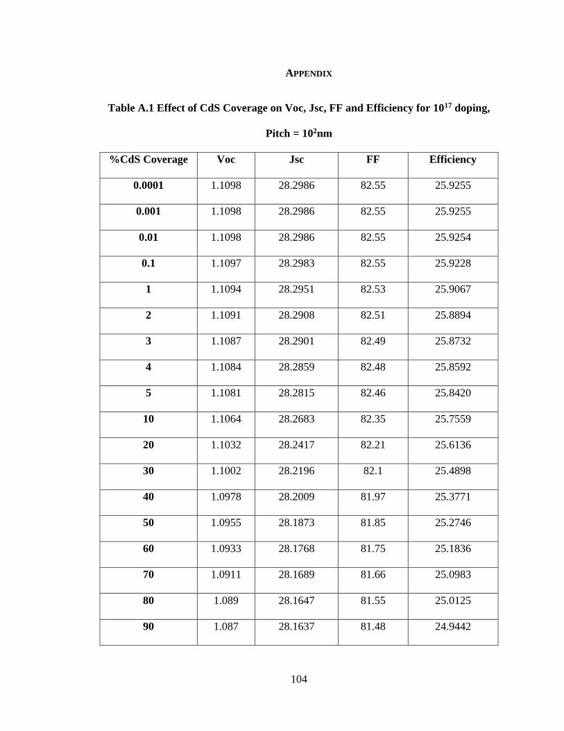
104
APPENDIX
Table A.1 Effect of CdS Coverage on Voc, Jsc, FF and Efficiency for 1017 doping,
Pitch = 102nm
%CdS Coverage Voc Jsc FF Efficiency
0.0001 1.1098 28.2986 82.55 25.9255
0.001 1.1098 28.2986 82.55 25.9255
0.01 1.1098 28.2986 82.55 25.9254
0.1 1.1097 28.2983 82.55 25.9228
1 1.1094 28.2951 82.53 25.9067
2 1.1091 28.2908 82.51 25.8894
3 1.1087 28.2901 82.49 25.8732
4 1.1084 28.2859 82.48 25.8592
5 1.1081 28.2815 82.46 25.8420
10 1.1064 28.2683 82.35 25.7559
20 1.1032 28.2417 82.21 25.6136
30 1.1002 28.2196 82.1 25.4898
40 1.0978 28.2009 81.97 25.3771
50 1.0955 28.1873 81.85 25.2746
60 1.0933 28.1768 81.75 25.1836
70 1.0911 28.1689 81.66 25.0983
80 1.089 28.1647 81.55 25.0125
90 1.087 28.1637 81.48 24.9442

105
100 1.085 28.1657 81.42 24.8818

106
Table A.2 Effect of CdS Coverage on Voc, Jsc, FF and Efficiency for 1016 CdTe
doping, Pitch = 102 nm
%CdS Coverage Voc Jsc FF Efficiency
0.0001 1.0563 28.2695 81.99 24.4831
0.001 1.0563 28.2695 81.99 24.4831
0.01 1.0563 28.2694 81.99 24.4830
0.1 1.0563 28.2690 81.98 24.4796
1 1.0561 28.2643 81.98 24.4710
2 1.0559 28.2584 81.98 24.4612
3 1.0557 28.2559 81.97 24.4515
4 1.0562 28.2490 81.98 24.4600
5 1.0562 28.2428 81.98 24.4547
10 1.0561 28.2200 81.97 24.4297
20 1.0558 28.1749 81.96 24.3807
30 1.0555 28.1349 81.95 24.3362
40 1.0553 28.0987 81.94 24.2973
50 1.055 28.0682 81.92 24.2581
60 1.0548 28.0412 81.91 24.2273
70 1.0545 28.0174 81.9 24.1968
80 1.0543 27.9976 81.89 24.1722
90 1.054 27.9814 81.87 24.1455
100 1.0538 27.9688 81.86 24.1270

107
Table A.3 Effect of CdS Coverage on Voc, Jsc, FF and Efficiency for 1015 CdTe
doping, Pitch = 102 nm
%CdS Coverage Voc Jsc FF Efficiency
0.0001 1.0057 28.2703 81.02 23.0352
0.001 1.0057 28.2703 81.02 23.0352
0.01 1.0057 28.2703 81.02 23.0351
0.1 1.0057 28.2697 81.02 23.0347
1 1.0057 28.2642 81.02 23.0302
2 1.0057 28.2574 81.02 23.0246
3 1.0057 28.2539 81.02 23.0218
4 1.0057 28.2472 81.02 23.0163
5 1.0057 28.2404 81.02 23.0108
10 1.0056 28.2142 81.02 22.9872
20 1.0055 28.1627 81.03 22.9457
30 1.0055 28.1164 81.03 22.9080
40 1.0054 28.0741 81.03 22.8713
50 1.0053 28.0377 81.04 22.8421
60 1.0052 28.0049 81.04 22.8132
70 1.0051 27.9754 81.04 22.7869
80 1.0051 27.9501 81.04 22.7663
90 1.005 27.9286 81.04 22.7465
100 1.005 27.9107 81.04 22.7319

108
Table A.4 Effect of CdS Coverage on Voc, Jsc, FF and Efficiency for 1014 CdTe
doping, Pitch = 102 nm
%CdS Coverage Voc Jsc FF Efficiency
0.0001 0.9808 28.2996 78.1 21.6776
0.001 0.9808 28.2996 78.1 21.6776
0.01 0.9808 28.2996 78.1 21.6776
0.1 0.9808 28.2990 78.1 21.6772
1 0.9808 28.2933 78.1 21.6728
2 0.9808 28.2862 78.1 21.6674
3 0.9808 28.2825 78.1 21.6645
4 0.9808 28.2755 78.1 21.6592
5 0.9808 28.2685 78.11 21.6566
10 0.9807 28.2412 78.11 21.6335
20 0.9806 28.1874 78.12 21.5928
30 0.9805 28.1388 78.13 21.5562
40 0.9804 28.0944 78.14 21.5227
50 0.9804 28.0558 78.15 21.4959
60 0.9803 28.0210 78.15 21.4670
70 0.9802 27.9895 78.16 21.4434
80 0.9801 27.9622 78.17 21.4231
90 0.9801 27.9387 78.17 21.4051
100 0.98 27.9190 78.2 21.3960

109
0.00001 0.0001 0.001 0.01 0.1 1
0.95
1.00
1.05
1.10
1.15
Voc vs % Coverage 0.0001-0.1%, L = 102
%CdS Coverage
Vo
c (
V)
Doping 1014
Doping 1015
Doping 1016
Doping 1017
Figure A.1 Voc vs 0.0001-0.1% CdS Coverage Interpore Distance 100nm
0.00001 0.0001 0.001 0.01 0.1 1
28.26
28.27
28.28
28.29
28.30
28.31
Jsc vs % Coverage 0.0001-0.1%, L = 102
%CdS Coverage
Js
c(m
A/c
m2)
Doping 1014
Doping 1015
Doping 1016
Doping 1017
Figure A.2 Jsc vs 0.0001-0.1% CdS Coverage Interpore Distance 100nm

110
0.00001 0.0001 0.001 0.01 0.1 1
77
78
79
80
81
82
83
FF vs % Coverage 0.0001-0.1%, L = 102
%CdS Coverage
Fill
Fa
cto
r (%
)Doping 1014
Doping 1015
Doping 1016
Doping 1017
Figure A.3 FF vs 0.0001-0.1% CdS Coverage Interpore Distance 100nm
0.00001 0.0001 0.001 0.01 0.1 1
21
22
23
24
25
26
27
Efficiency vs % Coverage 0.0001-0.1%, L = 102
%CdS Coverage
Eff
icie
nc
y(%
)
Doping 1014
Doping 1015
Doping 1016
Doping 1017
Figure A.4 Efficiency vs 0.0001-0.1% CdS Coverage Interpore Distance 100nm

111
1 2 3 4 5
0.95
1.00
1.05
1.10
1.15
20 40 60 80 100
Voc vs % Coverage 1-100%, L = 102
%CdS Coverage
Vo
c (
V)
Doping 1014
Doping 1015
Doping 1016
Doping 1017
Figure A.5 Voc vs 1-100% CdS Coverage Interpore Distance 100nm
1 2 3 4 5
27.8
27.9
28.0
28.1
28.2
28.3
28.4
20 40 60 80 100
Jsc vs % Coverage 1-100%, L = 102
%CdS Coverage
Js
c(m
A/c
m2)
Doping 1014
Doping 1015
Doping 1016
Doping 1017
Figure A.6 Jsc vs 1-100% CdS Coverage Interpore Distance 100nm
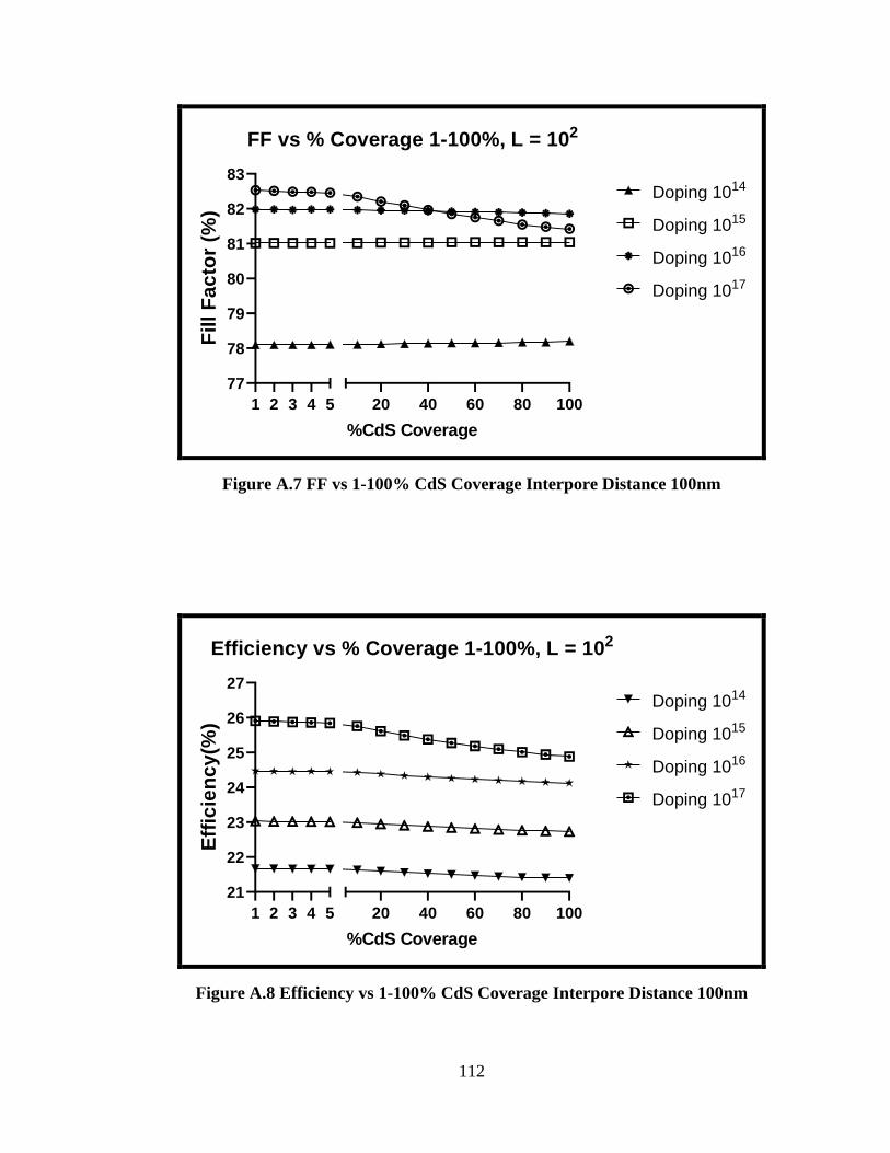
112
1 2 3 4 5
77
78
79
80
81
82
83
20 40 60 80 100
FF vs % Coverage 1-100%, L = 102
%CdS Coverage
Fill
Fa
cto
r (%
)Doping 1014
Doping 1015
Doping 1016
Doping 1017
Figure A.7 FF vs 1-100% CdS Coverage Interpore Distance 100nm
1 2 3 4 5
21
22
23
24
25
26
27
20 40 60 80 100
Efficiency vs % Coverage 1-100%, L = 102
%CdS Coverage
Eff
icie
nc
y(%
)
Doping 1014
Doping 1015
Doping 1016
Doping 1017
Figure A.8 Efficiency vs 1-100% CdS Coverage Interpore Distance 100nm
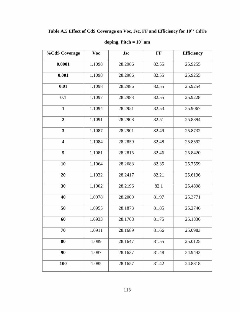
113
Table A.5 Effect of CdS Coverage on Voc, Jsc, FF and Efficiency for 1017 CdTe
doping, Pitch = 103 nm
%CdS Coverage Voc Jsc FF Efficiency
0.0001 1.1098 28.2986 82.55 25.9255
0.001 1.1098 28.2986 82.55 25.9255
0.01 1.1098 28.2986 82.55 25.9254
0.1 1.1097 28.2983 82.55 25.9228
1 1.1094 28.2951 82.53 25.9067
2 1.1091 28.2908 82.51 25.8894
3 1.1087 28.2901 82.49 25.8732
4 1.1084 28.2859 82.48 25.8592
5 1.1081 28.2815 82.46 25.8420
10 1.1064 28.2683 82.35 25.7559
20 1.1032 28.2417 82.21 25.6136
30 1.1002 28.2196 82.1 25.4898
40 1.0978 28.2009 81.97 25.3771
50 1.0955 28.1873 81.85 25.2746
60 1.0933 28.1768 81.75 25.1836
70 1.0911 28.1689 81.66 25.0983
80 1.089 28.1647 81.55 25.0125
90 1.087 28.1637 81.48 24.9442
100 1.085 28.1657 81.42 24.8818

114
Table A.6 Effect of CdS Coverage on Voc, Jsc, FF and Efficiency for 1016 CdTe
doping, Pitch = 103 nm
%CdS Coverage Voc Jsc FF Efficiency
0.0001 1.0563 28.2695 81.99 24.4831
0.001 1.0563 28.2695 81.99 24.4831
0.01 1.0563 28.2694 81.99 24.4830
0.1 1.0563 28.2690 81.98 24.4796
1 1.0561 28.2643 81.98 24.4710
2 1.0559 28.2584 81.98 24.4612
3 1.0557 28.2559 81.97 24.4515
4 1.0562 28.2490 81.98 24.4600
5 1.0562 28.2428 81.98 24.4547
10 1.0561 28.2200 81.97 24.4297
20 1.0558 28.1749 81.96 24.3807
30 1.0555 28.1349 81.95 24.3362
40 1.0553 28.0987 81.94 24.2973
50 1.055 28.0682 81.92 24.2581
60 1.0548 28.0412 81.91 24.2273
70 1.0545 28.0174 81.9 24.1968
80 1.0543 27.9976 81.89 24.1722
90 1.054 27.9814 81.87 24.1455
100 1.0538 27.9688 81.86 24.1270

115
Table A.7 Effect of CdS Coverage on Voc, Jsc, FF and Efficiency for 1015 CdTe
doping, Pitch = 103 nm
%CdS Coverage Voc Jsc FF Efficiency
0.0001 1.0057 28.2703 81.02 23.0352
0.001 1.0057 28.2703 81.02 23.0352
0.01 1.0057 28.2703 81.02 23.0351
0.1 1.0057 28.2697 81.02 23.0347
1 1.0057 28.2642 81.02 23.0302
2 1.0057 28.2574 81.02 23.0246
3 1.0057 28.2539 81.02 23.0218
4 1.0057 28.2472 81.02 23.0163
5 1.0057 28.2404 81.02 23.0108
10 1.0056 28.2142 81.02 22.9872
20 1.0055 28.1627 81.03 22.9457
30 1.0055 28.1164 81.03 22.9080
40 1.0054 28.0741 81.03 22.8713
50 1.0053 28.0377 81.04 22.8421
60 1.0052 28.0049 81.04 22.8132
70 1.0051 27.9754 81.04 22.7869
80 1.0051 27.9501 81.04 22.7663
90 1.005 27.9286 81.04 22.7465
100 1.005 27.9107 81.04 22.7319

116
Table A.8 Effect of CdS Coverage on Voc, Jsc, FF and Efficiency for 1014 CdTe
doping, Pitch = 103 nm
%CdS Coverage Voc Jsc FF Efficiency
0.0001 0.9808 28.2996 78.1 21.6776
0.001 0.9808 28.2996 78.1 21.6776
0.01 0.9808 28.2996 78.1 21.6776
0.1 0.9808 28.2990 78.1 21.6772
1 0.9808 28.2933 78.1 21.6728
2 0.9808 28.2862 78.1 21.6674
3 0.9808 28.2825 78.1 21.6645
4 0.9808 28.2755 78.1 21.6592
5 0.9808 28.2685 78.1 21.6538
10 0.9807 28.2412 78.11 21.6335
20 0.9806 28.1874 78.12 21.5928
30 0.9805 28.1388 78.13 21.5562
40 0.9804 28.0944 78.14 21.5227
50 0.9804 28.0558 78.14 21.4931
60 0.9803 28.0210 78.15 21.4670
70 0.9802 27.9895 78.16 21.4434
80 0.9801 27.9622 78.16 21.4203
90 0.9801 27.9387 78.17 21.4051
100 0.98 27.9190 78.2 21.3960

117
0.00001 0.0001 0.001 0.01 0.1 1
0.95
1.00
1.05
1.10
1.15
Voc vs % Coverage 0.0001-0.1%, L = 103
%CdS Coverage
Vo
c (
V)
Doping 1014
Doping 1015
Doping 1016
Doping 1017
Figure A.9 Voc vs 0.0001-0.1% CdS Coverage Interpore Distance 1µm
0.00001 0.0001 0.001 0.01 0.1 1
28.26
28.27
28.28
28.29
28.30
28.31
Jsc vs % Coverage 0.0001-0.1%, L = 103
%CdS Coverage
Js
c(m
A/c
m2)
Doping 1014
Doping 1015
Doping 1016
Doping 1017
Figure A.10 Jsc vs 0.0001-0.1% CdS Coverage Interpore Distance 1µm

118
0.00001 0.0001 0.001 0.01 0.1 1
77
78
79
80
81
82
83
FF vs % Coverage 0.0001-0.1%, L = 103
%CdS Coverage
Fill
Fa
cto
r (%
)Doping 1014
Doping 1015
Doping 1016
Doping 1017
Figure A.11 FF vs 0.0001-0.1% CdS Coverage Interpore Distance 1µm
0.00001 0.0001 0.001 0.01 0.1 1
21
22
23
24
25
26
27
Efficiency vs % Coverage 0.0001-0.1%, L = 103
%CdS Coverage
Eff
icie
nc
y(%
)
Doping 1014
Doping 1015
Doping 1016
Doping 1017
Figure A.12 Efficiency vs 0.0001-0.1% CdS Coverage Interpore Distance 1µm

119
0 1 2 3 4 5
0.95
1.00
1.05
1.10
1.15
20 40 60 80 100
Voc vs % Coverage 1-100%, L = 103
%CdS Coverage
Vo
c (
V)
Doping 1014
Doping 1015
Doping 1016
Doping 1017
Figure A.13 Voc vs 1-100% CdS Coverage Interpore Distance 1µm
0 1 2 3 4 5
27.8
27.9
28.0
28.1
28.2
28.3
28.4
20 40 60 80 100
Jsc vs % Coverage 1-100%, L = 103
%CdS Coverage
Js
c(m
A/c
m2)
Doping 1014
Doping 1015
Doping 1016
Doping 1017
Figure A.14 Jsc vs 1-100% CdS Coverage Interpore Distance 1µm

120
0 1 2 3 4 5
77
78
79
80
81
82
83
20 40 60 80 100
FF vs % Coverage 1-100%, L = 103
%CdS Coverage
Fill
Fa
cto
r (%
)Doping 1014
Doping 1015
Doping 1016
Doping 1017
Figure A.15 FF vs 1-100% CdS Coverage Interpore Distance 1µm
0 1 2 3 4 5
21
22
23
24
25
26
27
20 40 60 80 100
Efficiency vs % Coverage 1-100%, L = 103
%CdS Coverage
Eff
icie
nc
y(%
)
Doping 1014
Doping 1015
Doping 1016
Doping 1017
Figure A.16 Efficiency vs 1-100% CdS Coverage Interpore Distance 1µm

121
Table A.9 Effect of CdS Coverage on Voc, Jsc, FF and Efficiency for 1017 CdTe
doping, Pitch = 104 nm
%CdS Coverage Voc Jsc FF Efficiency
0.0001 1.1098 28.2986 82.55 25.9255
0.001 1.1098 28.2986 82.55 25.9255
0.01 1.1098 28.2986 82.55 25.9254
0.1 1.1097 28.2983 82.55 25.9228
1 1.1094 28.2951 82.53 25.9067
2 1.1091 28.2908 82.51 25.8894
3 1.1087 28.2901 82.49 25.8732
4 1.1084 28.2859 82.48 25.8592
5 1.1081 28.2815 82.46 25.8420
10 1.1064 28.2683 82.35 25.7559
20 1.1032 28.2417 82.21 25.6136
30 1.1002 28.2196 82.1 25.4898
40 1.0978 28.2009 81.97 25.3771
50 1.0955 28.1873 81.85 25.2746
60 1.0933 28.1768 81.75 25.1836
70 1.0911 28.1689 81.66 25.0983
80 1.089 28.1647 81.55 25.0125
90 1.087 28.1637 81.48 24.9442
100 1.085 28.1657 81.42 24.8818

122
Table A.10 Effect of CdS Coverage on Voc, Jsc, FF and Efficiency for 1016 CdTe
doping, Pitch = 104 nm
%CdS Coverage Voc Jsc FF Efficiency
0.0001 1.0563 28.2695 81.98 24.4801
0.001 1.0563 28.2695 81.98 24.4801
0.01 1.0563 28.2694 81.98 24.4800
0.1 1.0563 28.2690 81.98 24.4796
1 1.0561 28.2643 81.98 24.4710
2 1.0559 28.2584 81.98 24.4612
3 1.0557 28.2559 81.97 24.4515
4 1.0562 28.2490 81.98 24.4600
5 1.0562 28.2428 81.98 24.4547
10 1.0561 28.2200 81.97 24.4297
20 1.0558 28.1749 81.96 24.3807
30 1.0555 28.1349 81.95 24.3362
40 1.0553 28.0987 81.94 24.2973
50 1.055 28.0682 81.92 24.2581
60 1.0548 28.0412 81.91 24.2273
70 1.0545 28.0174 81.9 24.1968
80 1.0543 27.9976 81.89 24.1722
90 1.054 27.9814 81.87 24.1455
100 1.0538 27.9688 81.86 24.1270

123
Table A.11 Effect of CdS Coverage on Voc, Jsc, FF and Efficiency for 1015 CdTe
doping, Pitch = 104 nm
%CdS Coverage Voc Jsc FF Efficiency
0.0001 1.0057 28.2703 81.01 23.0323
0.001 1.0057 28.2703 81.01 23.0323
0.01 1.0057 28.2702 81.01 23.0323
0.1 1.0057 28.2697 81.01 23.0318
1 1.0057 28.2642 81.01 23.0273
2 1.0057 28.2574 81.01 23.0218
3 1.0057 28.2539 81.01 23.0189
4 1.0057 28.2472 81.02 23.0163
5 1.0057 28.2404 81.02 23.0108
10 1.0056 28.2142 81.02 22.9872
20 1.0055 28.1627 81.02 22.9429
30 1.0055 28.1164 81.03 22.9080
40 1.0054 28.0741 81.03 22.8713
50 1.0053 28.0376 81.03 22.8393
60 1.0052 28.0049 81.03 22.8104
70 1.0051 27.9754 81.04 22.7869
80 1.0051 27.9501 81.04 22.7663
90 1.005 27.9286 81.04 22.7465
100 1.005 27.9107 81.04 22.7319

124
Table A.12 Effect of CdS Coverage on Voc, Jsc, FF and Efficiency for 1014 CdTe
doping, Pitch = 104 nm
%CdS Coverage Voc Jsc FF Efficiency
0.0001 0.9808 28.2995 78.06 21.6664
0.001 0.9808 28.2995 78.06 21.6664
0.01 0.9808 28.2994 78.06 21.6664
0.1 0.9808 28.2988 78.06 21.6660
1 0.9808 28.2931 78.06 21.6616
2 0.9808 28.2861 78.06 21.6562
3 0.9808 28.2823 78.06 21.6533
4 0.9808 28.2754 78.07 21.6508
5 0.9808 28.2684 78.07 21.6454
10 0.9807 28.2411 78.08 21.6251
20 0.9806 28.1873 78.09 21.5844
30 0.9805 28.1387 78.1 21.5478
40 0.9804 28.0943 78.11 21.5143
50 0.9804 28.0557 78.12 21.4876
60 0.9803 28.0209 78.13 21.4615
70 0.9802 27.9894 78.14 21.4379
80 0.9801 27.9621 78.14 21.4148
90 0.9801 27.9386 78.15 21.3995
100 0.98 27.9190 78.2 21.3960

125
0.00001 0.0001 0.001 0.01 0.1 1
0.95
1.00
1.05
1.10
1.15
Voc vs % Coverage 0.0001-0.1%, L = 104
%CdS Coverage
Vo
c (
V)
Doping 1014
Doping 1015
Doping 1016
Doping 1017
Figure A.17 Voc vs 0.0001-0.1% CdS Coverage Interpore Distance 10µm
0.00001 0.0001 0.001 0.01 0.1 1
28.26
28.27
28.28
28.29
28.30
28.31
Jsc vs % Coverage 0.0001-0.1%, L = 104
%CdS Coverage
Js
c(m
A/c
m2)
Doping 1014
Doping 1015
Doping 1016
Doping 1017
Figure A.18 Jsc vs 0.0001-0.1% CdS Coverage Interpore Distance 10µm

126
0.00001 0.0001 0.001 0.01 0.1 1
77
78
79
80
81
82
83
FF vs % Coverage 0.0001-0.1%, L = 104
%CdS Coverage
Fill
Fa
cto
r (%
)Doping 1014
Doping 1015
Doping 1016
Doping 1017
Figure A.19 FF vs 0.0001-0.1% CdS Coverage Interpore Distance 10µm
0.00001 0.0001 0.001 0.01 0.1 1
21
22
23
24
25
26
27
Efficiency vs % Coverage 0.0001-0.1%, L = 104
%CdS Coverage
Eff
icie
nc
y(%
)
Doping 1014
Doping 1015
Doping 1016
Doping 1017
Figure A.20 Efficiency vs 0.0001-0.1% CdS Coverage Interpore Distance 10µm

127
0 1 2 3 4 5
0.95
1.00
1.05
1.10
1.15
20 40 60 80 100
Voc vs % Coverage 1-100%, L = 104
%CdS Coverage
Vo
c (
V)
Doping 1014
Doping 1015
Doping 1016
Doping 1017
Figure A.21 Voc vs 1-100% CdS Coverage Interpore Distance 10µm
0 1 2 3 4 5
27.8
27.9
28.0
28.1
28.2
28.3
28.4
20 40 60 80 100
Jsc vs % Coverage 1-100%, L = 104
%CdS Coverage
Js
c(m
A/c
m2)
Doping 1014
Doping 1015
Doping 1016
Doping 1017
Figure A.22 Jsc vs 1-100% CdS Coverage Interpore Distance 10µm
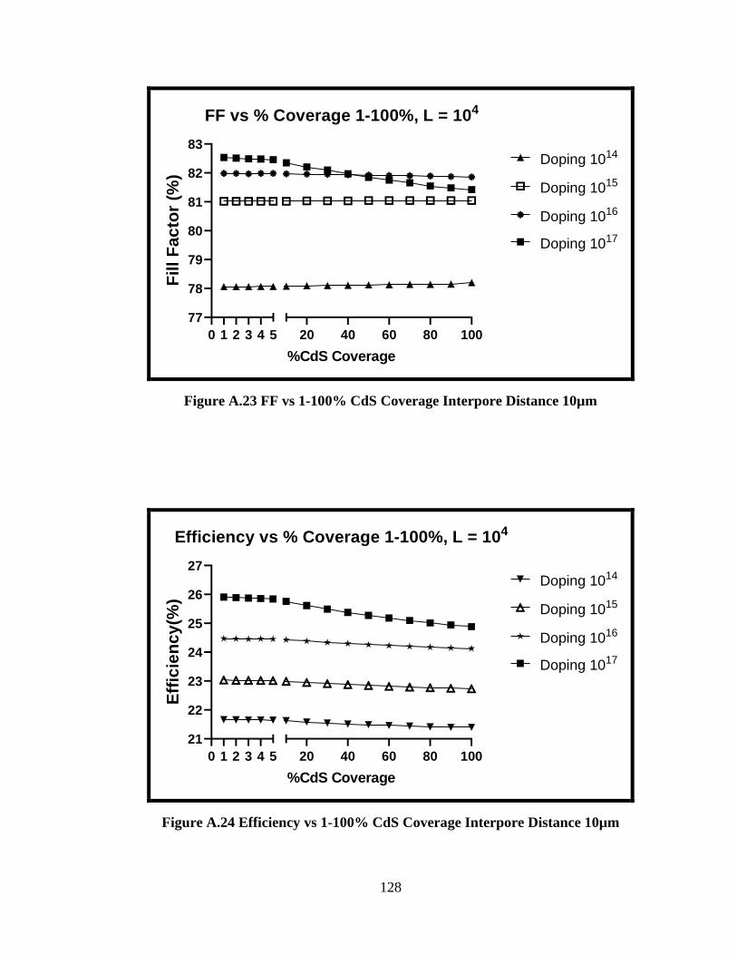
128
0 1 2 3 4 5
77
78
79
80
81
82
83
20 40 60 80 100
FF vs % Coverage 1-100%, L = 104
%CdS Coverage
Fill
Fa
cto
r (%
)Doping 1014
Doping 1015
Doping 1016
Doping 1017
Figure A.23 FF vs 1-100% CdS Coverage Interpore Distance 10µm
0 1 2 3 4 5
21
22
23
24
25
26
27
20 40 60 80 100
Efficiency vs % Coverage 1-100%, L = 104
%CdS Coverage
Eff
icie
nc
y(%
)
Doping 1014
Doping 1015
Doping 1016
Doping 1017
Figure A.24 Efficiency vs 1-100% CdS Coverage Interpore Distance 10µm

129
Table A.13 Effect of CdS Coverage on Voc, Jsc, FF and Efficiency for 1017 CdTe
doping, Pitch = 105 nm
%CdS Coverage Voc Jsc FF Efficiency
0.0001 1.1098 28.2986 82.55 25.9255
0.001 1.1098 28.2986 82.55 25.9255
0.01 1.1098 28.2986 82.55 25.9254
0.1 1.1097 28.2982 82.55 25.9228
1 1.1094 28.2951 82.53 25.9066
2 1.1091 28.2908 82.51 25.8894
3 1.1087 28.2901 82.49 25.8732
4 1.1084 28.2859 82.47 25.8560
5 1.1081 28.2815 82.46 25.8419
10 1.1064 28.2683 82.35 25.7558
20 1.1032 28.2417 82.21 25.6135
30 1.1002 28.2196 82.1 25.4898
40 1.0978 28.2009 81.96 25.3739
50 1.0955 28.1873 81.85 25.2746
60 1.0933 28.1768 81.75 25.1836
70 1.0911 28.1689 81.66 25.0983
80 1.089 28.1647 81.55 25.0125
90 1.087 28.1637 81.48 24.9442
100 1.085 28.1657 81.42 24.8818

130
Table A.14 Effect of CdS Coverage on Voc, Jsc, FF and Efficiency for 1016 CdTe
doping, Pitch = 105 nm
%CdS Coverage Voc Jsc FF Efficiency
0.0001 1.0563 28.2694 81.98 24.4801
0.001 1.0563 28.2694 81.98 24.4801
0.01 1.0563 28.2694 81.98 24.4800
0.1 1.0563 28.2689 81.98 24.4796
1 1.0561 28.2643 81.98 24.4709
2 1.0559 28.2584 81.97 24.4582
3 1.0557 28.2559 81.97 24.4514
4 1.0562 28.2490 81.98 24.4600
5 1.0562 28.2428 81.98 24.4547
10 1.0561 28.2200 81.97 24.4297
20 1.0558 28.1749 81.96 24.3807
30 1.0555 28.1349 81.95 24.3362
40 1.0553 28.0987 81.93 24.2943
50 1.055 28.0682 81.92 24.2581
60 1.0548 28.0412 81.91 24.2273
70 1.0545 28.0174 81.9 24.1968
80 1.0543 27.9976 81.88 24.1692
90 1.054 27.9814 81.87 24.1455
100 1.0538 27.9688 81.86 24.1270

131
Table A.15 Effect of CdS Coverage on Voc, Jsc, FF and Efficiency for 1015 CdTe
doping, Pitch = 105 nm
%CdS Coverage Voc Jsc FF Efficiency
0.0001 1.0057 28.2702 80.97 23.0208
0.001 1.0057 28.2701 80.97 23.0208
0.01 1.0057 28.2701 80.98 23.0236
0.1 1.0057 28.2696 80.98 23.0232
1 1.0057 28.2641 80.98 23.0187
2 1.0057 28.2572 80.98 23.0131
3 1.0057 28.2537 80.98 23.0103
4 1.0057 28.2470 80.98 23.0048
5 1.0057 28.2402 80.98 22.9993
10 1.0056 28.2141 80.99 22.9786
20 1.0055 28.1626 80.99 22.9343
30 1.0055 28.1163 81 22.8994
40 1.0054 28.0740 81.01 22.8655
50 1.0053 28.0376 81.01 22.8336
60 1.0052 28.0048 81.01 22.8047
70 1.0051 27.9753 81.02 22.7812
80 1.0051 27.9500 81.02 22.7606
90 1.005 27.9285 81.02 22.7408
100 1.005 27.9107 81.04 22.7319

132
Table A.16 Effect of CdS Coverage on Voc, Jsc, FF and Efficiency for 1014 CdTe
doping, Pitch = 105 nm
%CdS Coverage Voc Jsc FF Efficiency
0.0001 0.9808 28.2980 77.68 21.5599
0.001 0.9808 28.2980 77.68 21.5598
0.01 0.9808 28.2980 77.68 21.5598
0.1 0.9808 28.2974 77.68 21.5594
1 0.9808 28.2918 77.7 21.5606
2 0.9808 28.2848 77.71 21.5581
3 0.9808 28.2810 77.72 21.5580
4 0.9808 28.2741 77.73 21.5555
5 0.9808 28.2671 77.73 21.5502
10 0.9807 28.2399 77.76 21.5355
20 0.9806 28.1862 77.8 21.5034
30 0.9805 28.1377 77.83 21.4725
40 0.9804 28.0933 77.86 21.4447
50 0.9804 28.0548 77.88 21.4209
60 0.9803 28.0201 77.91 21.4004
70 0.9802 27.9886 77.93 21.3796
80 0.9801 27.9614 77.94 21.3594
90 0.9801 27.9379 77.96 21.3470
100 0.98 27.9190 78.2 21.3960

133
0.00001 0.0001 0.001 0.01 0.1 1
0.95
1.00
1.05
1.10
1.15
Voc vs % Coverage 0.0001-0.1%, L = 105
%CdS Coverage
Vo
c (
V)
Doping 1014
Doping 1015
Doping 1016
Doping 1017
Figure A.25 Voc vs 0.0001-0.1% CdS Coverage Interpore Distance 100µm
0.00001 0.0001 0.001 0.01 0.1 1
28.26
28.27
28.28
28.29
28.30
28.31
Jsc vs % Coverage 0.0001-0.1%, L = 105
%CdS Coverage
Js
c(m
A/c
m2)
Doping 1014
Doping 1015
Doping 1016
Doping 1017
Figure A.26 Jsc vs 0.0001-0.1% CdS Coverage Interpore Distance 100µm
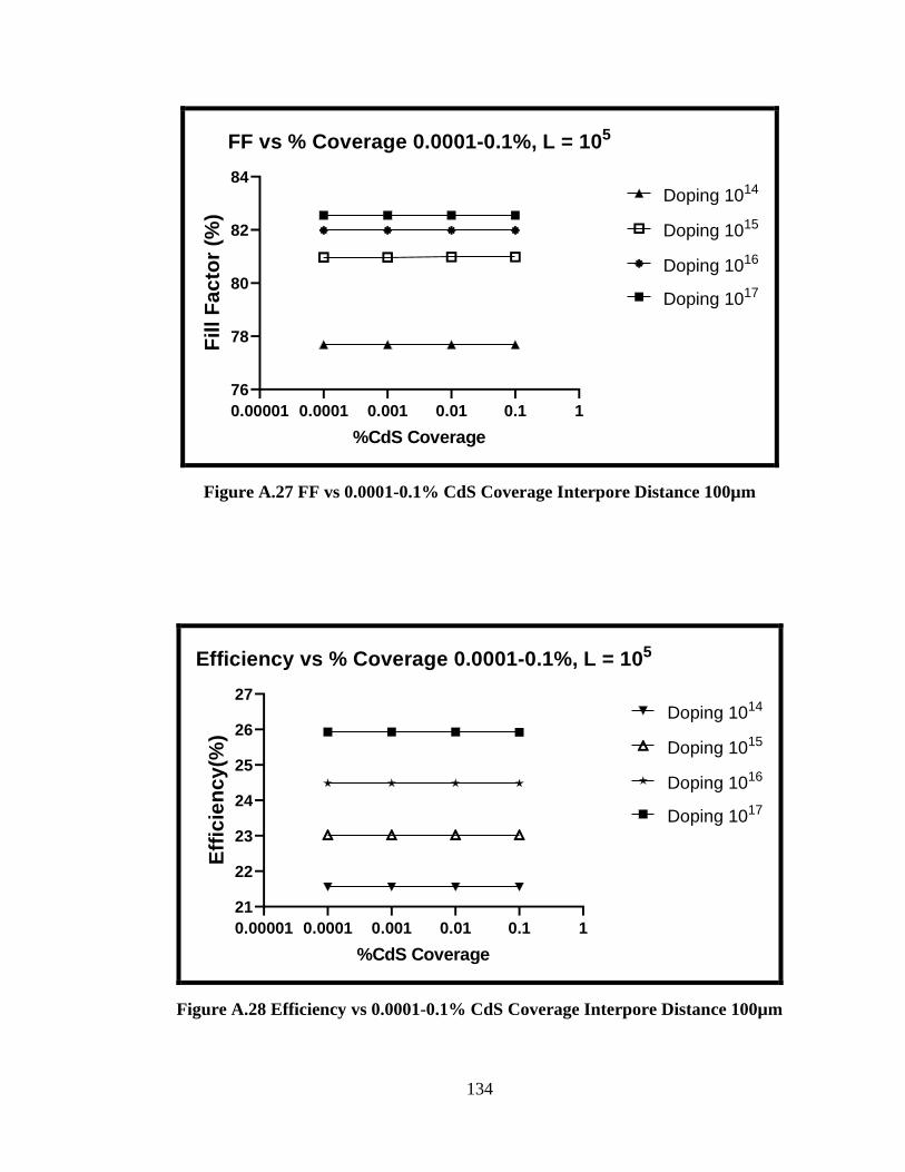
134
0.00001 0.0001 0.001 0.01 0.1 1
76
78
80
82
84
FF vs % Coverage 0.0001-0.1%, L = 105
%CdS Coverage
Fill
Fa
cto
r (%
)Doping 1014
Doping 1015
Doping 1016
Doping 1017
Figure A.27 FF vs 0.0001-0.1% CdS Coverage Interpore Distance 100µm
0.00001 0.0001 0.001 0.01 0.1 1
21
22
23
24
25
26
27
Efficiency vs % Coverage 0.0001-0.1%, L = 105
%CdS Coverage
Eff
icie
nc
y(%
)
Doping 1014
Doping 1015
Doping 1016
Doping 1017
Figure A.28 Efficiency vs 0.0001-0.1% CdS Coverage Interpore Distance 100µm

135
0 1 2 3 4 5
0.95
1.00
1.05
1.10
1.15
20 40 60 80 100
Voc vs % Coverage 1-100%, L = 105
%CdS Coverage
Vo
c (
V)
Doping 1014
Doping 1015
Doping 1016
Doping 1017
Figure A.29 Voc vs 1-100% CdS Coverage Interpore Distance 100µm
0 1 2 3 4 5
27.8
27.9
28.0
28.1
28.2
28.3
28.4
20 40 60 80 100
Jsc vs % Coverage 1-100%, L = 105
%CdS Coverage
Js
c(m
A/c
m2)
Doping 1014
Doping 1015
Doping 1016
Doping 1017
Figure A.30 Jsc vs 1-100% CdS Coverage Interpore Distance 100µm
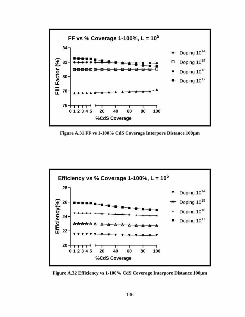
136
0 1 2 3 4 5
76
78
80
82
84
20 40 60 80 100
FF vs % Coverage 1-100%, L = 105
%CdS Coverage
Fill
Fa
cto
r (%
)Doping 1014
Doping 1015
Doping 1016
Doping 1017
Figure A.31 FF vs 1-100% CdS Coverage Interpore Distance 100µm
0 1 2 3 4 5
20
22
24
26
28
20 40 60 80 100
Efficiency vs % Coverage 1-100%, L = 105
%CdS Coverage
Eff
icie
nc
y(%
)
Doping 1014
Doping 1015
Doping 1016
Doping 1017
Figure A.32 Efficiency vs 1-100% CdS Coverage Interpore Distance 100µm
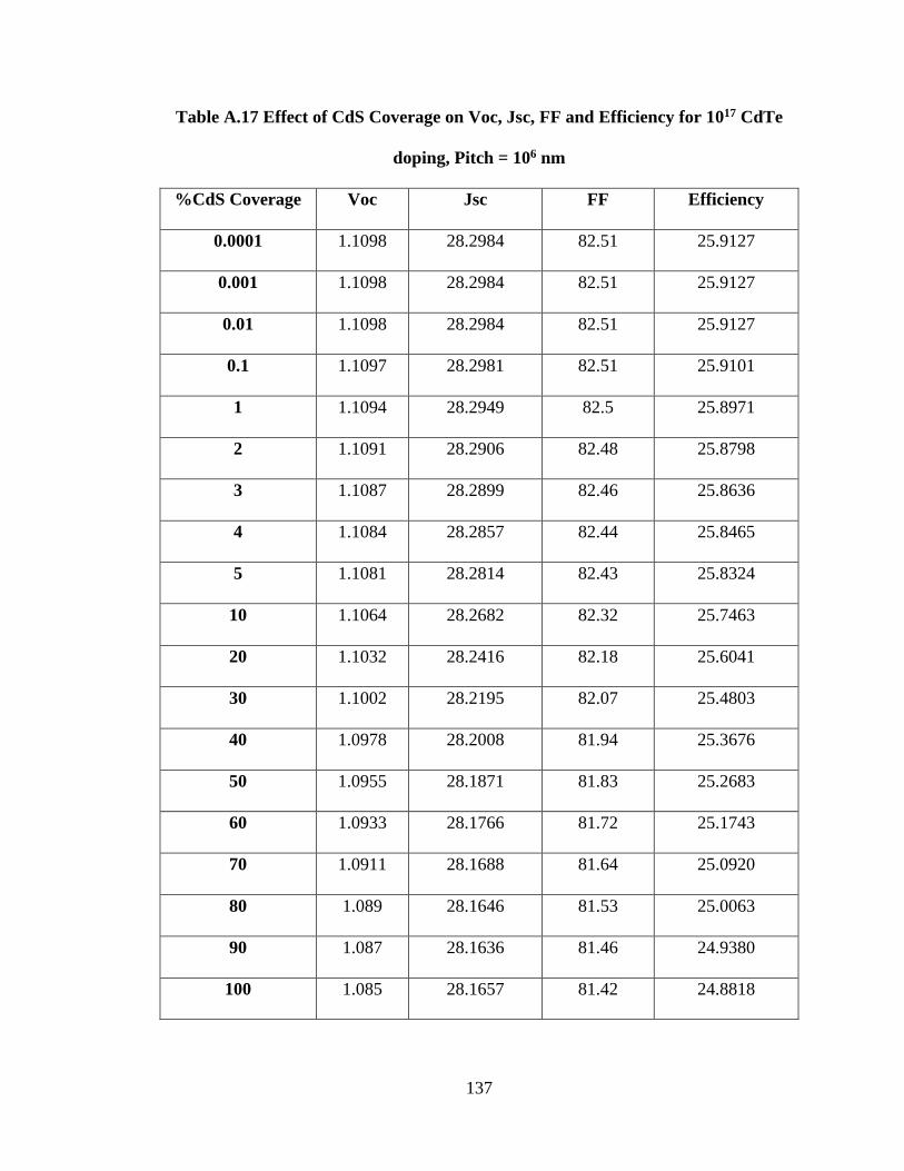
137
Table A.17 Effect of CdS Coverage on Voc, Jsc, FF and Efficiency for 1017 CdTe
doping, Pitch = 106 nm
%CdS Coverage Voc Jsc FF Efficiency
0.0001 1.1098 28.2984 82.51 25.9127
0.001 1.1098 28.2984 82.51 25.9127
0.01 1.1098 28.2984 82.51 25.9127
0.1 1.1097 28.2981 82.51 25.9101
1 1.1094 28.2949 82.5 25.8971
2 1.1091 28.2906 82.48 25.8798
3 1.1087 28.2899 82.46 25.8636
4 1.1084 28.2857 82.44 25.8465
5 1.1081 28.2814 82.43 25.8324
10 1.1064 28.2682 82.32 25.7463
20 1.1032 28.2416 82.18 25.6041
30 1.1002 28.2195 82.07 25.4803
40 1.0978 28.2008 81.94 25.3676
50 1.0955 28.1871 81.83 25.2683
60 1.0933 28.1766 81.72 25.1743
70 1.0911 28.1688 81.64 25.0920
80 1.089 28.1646 81.53 25.0063
90 1.087 28.1636 81.46 24.9380
100 1.085 28.1657 81.42 24.8818

138
Table A.18 Effect of CdS Coverage on Voc, Jsc, FF and Efficiency for 1016 CdTe
doping, Pitch = 106 nm
%CdS Coverage Voc Jsc FF Efficiency
0.0001 1.0563 28.2693 81.95 24.4710
0.001 1.0563 28.2693 81.95 24.4710
0.01 1.0563 28.2692 81.95 24.4709
0.1 1.0563 28.2688 81.95 24.4705
1 1.0561 28.2641 81.94 24.4589
2 1.0559 28.2582 81.94 24.4492
3 1.0557 28.2557 81.94 24.4424
4 1.0562 28.2488 81.94 24.4480
5 1.0562 28.2427 81.94 24.4426
10 1.0561 28.2199 81.94 24.4206
20 1.0558 28.1748 81.93 24.3717
30 1.0555 28.1347 81.92 24.3271
40 1.0553 28.0986 81.91 24.2883
50 1.055 28.0681 81.9 24.2521
60 1.0548 28.0411 81.89 24.2212
70 1.0545 28.0173 81.88 24.1908
80 1.0543 27.9975 81.86 24.1633
90 1.054 27.9813 81.85 24.1395
100 1.0538 27.9688 81.86 24.1270
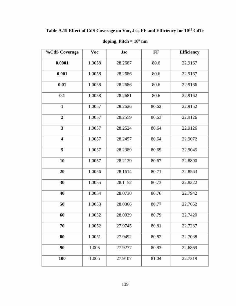
139
Table A.19 Effect of CdS Coverage on Voc, Jsc, FF and Efficiency for 1015 CdTe
doping, Pitch = 106 nm
%CdS Coverage Voc Jsc FF Efficiency
0.0001 1.0058 28.2687 80.6 22.9167
0.001 1.0058 28.2686 80.6 22.9167
0.01 1.0058 28.2686 80.6 22.9166
0.1 1.0058 28.2681 80.6 22.9162
1 1.0057 28.2626 80.62 22.9152
2 1.0057 28.2559 80.63 22.9126
3 1.0057 28.2524 80.64 22.9126
4 1.0057 28.2457 80.64 22.9072
5 1.0057 28.2389 80.65 22.9045
10 1.0057 28.2129 80.67 22.8890
20 1.0056 28.1614 80.71 22.8563
30 1.0055 28.1152 80.73 22.8222
40 1.0054 28.0730 80.76 22.7942
50 1.0053 28.0366 80.77 22.7652
60 1.0052 28.0039 80.79 22.7420
70 1.0052 27.9745 80.81 22.7237
80 1.0051 27.9492 80.82 22.7038
90 1.005 27.9277 80.83 22.6869
100 1.005 27.9107 81.04 22.7319

140
Table A.20 Effect of CdS Coverage on Voc, Jsc, FF and Efficiency for 1014 CdTe
doping, Pitch = 106 nm
%CdS Coverage Voc Jsc FF Efficiency
0.0001 0.9809 28.2836 73.88 20.4968
0.001 0.9809 28.2836 73.88 20.4968
0.01 0.9809 28.2836 73.9 20.5023
0.1 0.9809 28.2832 73.95 20.5159
1 0.9808 28.2781 74.1 20.5517
2 0.9808 28.2714 74.2 20.5746
3 0.9808 28.2679 74.27 20.5915
4 0.9808 28.2612 74.33 20.6032
5 0.9808 28.2544 74.39 20.6149
10 0.9807 28.2278 74.6 20.6515
20 0.9806 28.1751 74.9 20.6938
30 0.9805 28.1274 75.14 20.7228
40 0.9804 28.0837 75.34 20.7436
50 0.9804 28.0458 75.51 20.7623
60 0.9803 28.0115 75.67 20.7788
70 0.9802 27.9805 75.82 20.7948
80 0.9801 27.9537 75.95 20.8084
90 0.9801 27.9307 76.08 20.8268
100 0.98 27.9190 78.2 21.3960

141
0.00001 0.0001 0.001 0.01 0.1 1
0.95
1.00
1.05
1.10
1.15
Voc vs % Coverage 0.0001-0.1%, L = 106
%CdS Coverage
Vo
c (
V)
Doping 1014
Doping 1015
Doping 1016
Doping 1017
Figure A.33 Voc vs 0.0001-0.1% CdS Coverage Interpore Distance 1mm
0.00001 0.0001 0.001 0.01 0.1 1
28.26
28.27
28.28
28.29
28.30
Jsc vs % Coverage 0.0001-0.1%, L = 106
%CdS Coverage
Js
c(m
A/c
m2)
Doping 1014
Doping 1015
Doping 1016
Doping 1017
Figure A.34 Jsc vs 0.0001-0.1% CdS Coverage Interpore Distance 1mm

142
0.00001 0.0001 0.001 0.01 0.1 1
72
74
76
78
80
82
84
FF vs % Coverage 0.0001-0.1%, L = 106
%CdS Coverage
Fill
Fa
cto
r (%
)Doping 1014
Doping 1015
Doping 1016
Doping 1017
Figure A.35 FF vs 0.0001-0.1% CdS Coverage Interpore Distance 1mm
0.00001 0.0001 0.001 0.01 0.1 1
20
22
24
26
28
Efficiency vs % Coverage 0.0001-0.1%, L = 106
%CdS Coverage
Eff
icie
nc
y(%
)
Doping 1014
Doping 1015
Doping 1016
Doping 1017
Figure A.36 Efficiency vs 0.0001-0.1% CdS Coverage Interpore Distance 1mm

143
0 1 2 3 4 5
0.95
1.00
1.05
1.10
1.15
20 40 60 80 100
Voc vs % Coverage 1-100%, L = 106
%CdS Coverage
Vo
c (
V)
Doping 1014
Doping 1015
Doping 1016
Doping 1017
Figure A.37 Voc vs 1-100% CdS Coverage Interpore Distance 1mm
0 1 2 3 4 5
27.8
27.9
28.0
28.1
28.2
28.3
28.4
20 40 60 80 100
Jsc vs % Coverage 1-100%, L = 106
%CdS Coverage
Js
c(m
A/c
m2)
Doping 1014
Doping 1015
Doping 1016
Doping 1017
Figure A.38 Jsc vs 1-100% CdS Coverage Interpore Distance 1mm

144
0 1 2 3 4 5
72
74
76
78
80
82
84
20 40 60 80 100
FF vs % Coverage 1-100%, L = 106
%CdS Coverage
Fill
Fa
cto
r (%
)Doping 1014
Doping 1015
Doping 1016
Doping 1017
Figure A.39 FF vs 1-100% CdS Coverage Interpore Distance 1mm
0 1 2 3 4 5
20
22
24
26
28
20 40 60 80 100
Efficiency vs % Coverage 1-100%, L = 106
%CdS Coverage
Eff
icie
nc
y(%
)
Doping 1014
Doping 1015
Doping 1016
Doping 1017
Figure A.40 Efficiency vs 1-100% CdS Coverage Interpore Distance 1mm

145
Table A.21 Effect of CdS Coverage on Voc, Jsc, FF and Efficiency for 1017 CdTe
doping, Pitch = 107 nm
%CdS Coverage Voc Jsc FF Efficiency
0.0001 1.1098 28.2966 82.17 25.8043
0.001 1.1098 28.2966 82.17 25.8043
0.01 1.1098 28.2966 82.17 25.8043
0.1 1.1098 28.2963 82.18 25.8072
1 1.1095 28.2932 82.17 25.7943
2 1.1091 28.2889 82.16 25.7779
3 1.1088 28.2883 82.15 25.7672
4 1.1084 28.2841 82.14 25.7509
5 1.1081 28.2798 82.13 25.7369
10 1.1064 28.2666 82.03 25.6542
20 1.1032 28.2401 81.92 25.5218
30 1.1002 28.2181 81.83 25.4046
40 1.0978 28.1994 81.71 25.2952
50 1.0955 28.1859 81.61 25.1992
60 1.0933 28.1754 81.52 25.1116
70 1.0912 28.1676 81.45 25.0349
80 1.0891 28.1635 81.35 24.9524
90 1.087 28.1625 81.29 24.8850
100 1.085 28.1657 81.42 24.8818

146
Table A.22 Effect of CdS Coverage on Voc, Jsc, FF and Efficiency for 1016 CdTe
doping, Pitch = 107 nm
%CdS Coverage Voc Jsc FF Efficiency
0.0001 1.0564 28.2677 81.59 24.3644
0.001 1.0564 28.2677 81.59 24.3644
0.01 1.0564 28.2676 81.59 24.3643
0.1 1.0563 28.2672 81.59 24.3617
1 1.0561 28.2626 81.6 24.3561
2 1.0559 28.2567 81.61 24.3494
3 1.0557 28.2543 81.61 24.3427
4 1.0562 28.2474 81.62 24.3512
5 1.0562 28.2412 81.63 24.3489
10 1.0561 28.2185 81.64 24.3300
20 1.0558 28.1735 81.66 24.2903
30 1.0556 28.1336 81.67 24.2542
40 1.0553 28.0975 81.67 24.2162
50 1.0551 28.0670 81.67 24.1853
60 1.0548 28.0401 81.68 24.1583
70 1.0545 28.0163 81.68 24.1309
80 1.0543 27.9966 81.68 24.1093
90 1.0541 27.9805 81.68 24.0909
100 1.0538 27.9688 81.86 24.1270

147
Table A.23 Effect of CdS Coverage on Voc, Jsc, FF and Efficiency for 1015 CdTe
doping, Pitch = 107 nm
%CdS Coverage Voc Jsc FF Efficiency
0.0001 1.0059 28.2536 76.91 21.8581
0.001 1.0059 28.2536 76.92 21.8609
0.01 1.0059 28.2536 76.93 21.8638
0.1 1.0059 28.2533 76.98 21.8777
1 1.0058 28.2484 77.13 21.9143
2 1.0058 28.2419 77.22 21.9349
3 1.0058 28.2387 77.29 21.9523
4 1.0058 28.2322 77.35 21.9643
5 1.0058 28.2256 77.4 21.9733
10 1.0057 28.2003 77.61 22.0110
20 1.0056 28.1499 77.84 22.0346
30 1.0055 28.1044 78.07 22.0618
40 1.0055 28.0629 78.26 22.0828
50 1.0054 28.0271 78.43 22.1003
60 1.0053 27.9949 78.58 22.1150
70 1.0052 27.9659 78.72 22.1292
80 1.0051 27.9411 78.85 22.1440
90 1.0051 27.9201 78.97 22.1609
100 1.005 27.9107 81.04 22.7319

148
Table A.24 Effect of CdS Coverage on Voc, Jsc, FF and Efficiency for 1014 CdTe
doping, Pitch = 107 nm
%CdS Coverage Voc Jsc FF Efficiency
0.0001 0.9809 28.1345 40.95 11.3010
0.001 0.9809 28.1347 40.99 11.3121
0.01 0.9809 28.1353 41.09 11.3400
0.1 0.9809 28.1367 41.42 11.4316
1 0.9809 28.1372 42.49 11.7272
2 0.9808 28.1340 43.15 11.9067
3 0.9808 28.1331 43.66 12.0471
4 0.9808 28.1286 44.1 12.1666
5 0.9808 28.1238 44.49 12.2720
10 0.9808 28.1048 45.68 12.5918
20 0.9806 28.0627 48.14 13.2473
30 0.9805 28.0231 50.07 13.7576
40 0.9805 27.9861 51.71 14.1894
50 0.9804 27.9541 53.18 14.5746
60 0.9803 27.9251 54.26 14.8537
70 0.9802 27.8989 55.55 15.1910
80 0.9802 27.8767 56.76 15.5095
90 0.9801 27.8578 57.89 15.8060
100 0.98 27.9190 78.2 21.3960

149
0.00001 0.0001 0.001 0.01 0.1 1
0.95
1.00
1.05
1.10
1.15
Voc vs % Coverage 0.0001-0.1%, L = 107
%CdS Coverage
Vo
c (
V)
Doping 1014
Doping 1015
Doping 1016
Doping 1017
Figure A.41 Voc vs 0.0001-0.1% CdS Coverage Interpore Distance 10mm
0.00001 0.0001 0.001 0.01 0.1 1
28.10
28.15
28.20
28.25
28.30
28.35
Jsc vs % Coverage 0.0001-0.1%, L = 107
%CdS Coverage
Js
c(m
A/c
m2)
Doping 1014
Doping 1015
Doping 1016
Doping 1017
Figure A.42 Jsc vs 0.0001-0.1% CdS Coverage Interpore Distance 10mm

150
0.00001 0.0001 0.001 0.01 0.1 1
0
20
40
60
80
100
FF vs % Coverage 0.0001-0.1%, L = 107
%CdS Coverage
Fill
Fa
cto
r (%
)Doping 1014
Doping 1015
Doping 1016
Doping 1017
Figure A.43 FF vs 0.0001-0.1% CdS Coverage Interpore Distance 10mm
0.00001 0.0001 0.001 0.01 0.1 1
0
10
20
30
Efficiency vs % Coverage 0.0001-0.1%, L = 107
%CdS Coverage
Eff
icie
nc
y(%
)
Doping 1014
Doping 1015
Doping 1016
Doping 1017
Figure A.44 Efficiency vs 0.0001-0.1% CdS Coverage Interpore Distance 10mm

151
0 1 2 3 4 5
0.95
1.00
1.05
1.10
1.15
20 40 60 80 100
Voc vs % Coverage 1-100%, L = 107
%CdS Coverage
Vo
c (
V)
Doping 1014
Doping 1015
Doping 1016
Doping 1017
Figure A.45 Voc vs 1-100% CdS Coverage Interpore Distance 10mm
0 1 2 3 4 5
27.8
27.9
28.0
28.1
28.2
28.3
28.4
20 40 60 80 100
Jsc vs % Coverage 1-100%, L = 107
%CdS Coverage
Js
c(m
A/c
m2)
Doping 1014
Doping 1015
Doping 1016
Doping 1017
Figure A.46 Jsc vs 1-100% CdS Coverage Interpore Distance 10mm

152
0 1 2 3 4 5
0
20
40
60
80
100
20 40 60 80 100
FF vs % Coverage 1-100%, L = 107
%CdS Coverage
Fill
Fa
cto
r (%
)Doping 1014
Doping 1015
Doping 1016
Doping 1017
Figure A.47 FF vs 1-100% CdS Coverage Interpore Distance 10mm
0 1 2 3 4 5
0
10
20
30
20 40 60 80 100
Efficiency vs % Coverage 1-100%, L = 107
%CdS Coverage
Eff
icie
nc
y(%
)
Doping 1014
Doping 1015
Doping 1016
Doping 1017
Figure A.48 Efficiency vs 1-100% CdS Coverage Interpore Distance 10mm

153
Table A.25 Effect of CdS Coverage on Voc, Jsc, FF and Efficiency for 1017 CdTe
doping, Pitch = 108 nm
%CdS Coverage Voc Jsc FF Efficiency
0.0001 1.1101 28.2787 78.78 24.7308
0.001 1.1101 28.2787 78.79 24.7339
0.01 1.1101 28.2788 78.8 24.7371
0.1 1.1101 28.2787 78.84 24.7496
1 1.1097 28.2762 78.96 24.7761
2 1.1094 28.2722 79.02 24.7848
3 1.109 28.2718 79.07 24.7912
4 1.1087 28.2678 79.11 24.7935
5 1.1083 28.2637 79.14 24.7904
10 1.1066 28.2513 79.24 24.7727
20 1.1033 28.2256 79.33 24.7044
30 1.1002 28.2043 79.42 24.6443
40 1.0979 28.1862 79.45 24.5863
50 1.0957 28.1731 79.48 24.5349
60 1.0935 28.1631 79.51 24.4862
70 1.0913 28.1558 79.54 24.4398
80 1.0892 28.1520 79.54 24.3895
90 1.0871 28.1514 79.58 24.3542
100 1.085 28.1657 81.42 24.8818

154
Table A.26 Effect of CdS Coverage on Voc, Jsc, FF and Efficiency for 1016 CdTe
doping, Pitch = 108 nm
%CdS Coverage Voc Jsc FF Efficiency
0.0001 1.0566 28.2515 78.01 23.2864
0.001 1.0566 28.2515 78.02 23.2894
0.01 1.0566 28.2515 78.03 23.2924
0.1 1.0566 28.2513 78.07 23.3041
1 1.0564 28.2472 78.21 23.3381
2 1.0562 28.2417 78.3 23.3560
3 1.056 28.2395 78.36 23.3677
4 1.0565 28.2328 78.42 23.3911
5 1.0565 28.2269 78.47 23.4011
10 1.0563 28.2049 78.66 23.4350
20 1.056 28.1609 78.93 23.4721
30 1.0558 28.1217 79.13 23.4944
40 1.0555 28.0863 79.3 23.5085
50 1.0553 28.0564 79.44 23.5205
60 1.055 28.0300 79.57 23.5302
70 1.0547 28.0067 79.69 23.5393
80 1.0545 27.9874 79.8 23.5512
90 1.0542 27.9717 79.9 23.5607
100 1.0538 27.9688 81.86 24.1270
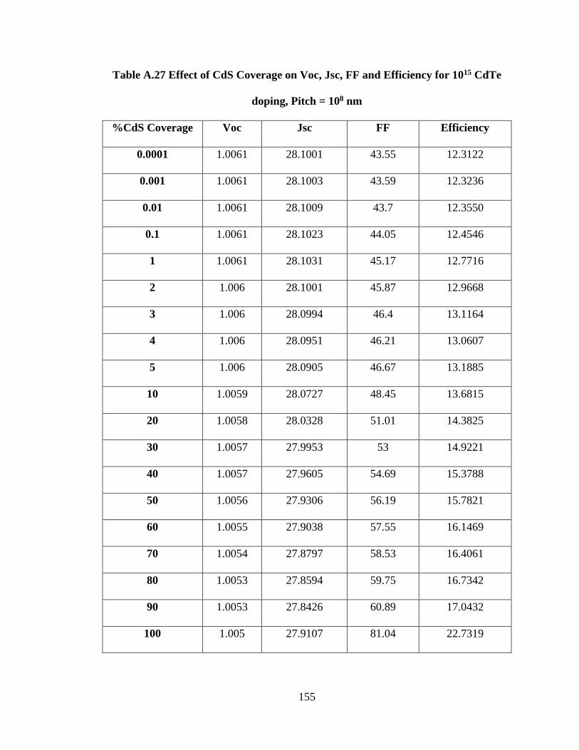
155
Table A.27 Effect of CdS Coverage on Voc, Jsc, FF and Efficiency for 1015 CdTe
doping, Pitch = 108 nm
%CdS Coverage Voc Jsc FF Efficiency
0.0001 1.0061 28.1001 43.55 12.3122
0.001 1.0061 28.1003 43.59 12.3236
0.01 1.0061 28.1009 43.7 12.3550
0.1 1.0061 28.1023 44.05 12.4546
1 1.0061 28.1031 45.17 12.7716
2 1.006 28.1001 45.87 12.9668
3 1.006 28.0994 46.4 13.1164
4 1.006 28.0951 46.21 13.0607
5 1.006 28.0905 46.67 13.1885
10 1.0059 28.0727 48.45 13.6815
20 1.0058 28.0328 51.01 14.3825
30 1.0057 27.9953 53 14.9221
40 1.0057 27.9605 54.69 15.3788
50 1.0056 27.9306 56.19 15.7821
60 1.0055 27.9038 57.55 16.1469
70 1.0054 27.8797 58.53 16.4061
80 1.0053 27.8594 59.75 16.7342
90 1.0053 27.8426 60.89 17.0432
100 1.005 27.9107 81.04 22.7319

156
Table A.28 Effect of CdS Coverage on Voc, Jsc, FF and Efficiency for 1014 CdTe
doping, Pitch = 108 nm
%CdS Coverage Voc Jsc FF Efficiency
0.0001 0.9809 5.844030 28.26 1.6200
0.001 0.9809 5.850514 28.26 1.6218
0.01 0.9809 5.871115 28.26 1.6275
0.1 0.9809 5.937216 28.25 1.6452
1 0.9809 6.156327 28.23 1.7047
2 0.9808 6.297037 28.22 1.7429
3 0.9808 6.409457 28.21 1.7734
4 0.9808 6.507338 28.2 1.7998
5 0.9808 6.596065 28.19 1.8237
10 0.9808 6.968813 28.16 1.9247
20 0.9807 7.573626 28.08 2.0856
30 0.9806 8.113594 28 2.2277
40 0.9805 8.632146 27.91 2.3623
50 0.9804 9.146975 27.81 2.4939
60 0.9803 9.668021 27.7 2.6253
70 0.9802 10.202180 27.58 2.7580
0 0.9802 10.758009 19.31 2.0362
90 0.9801 11.337253 20.13 2.2368
100 0.9800 27.91899200 78.2 21.3960

157
0.00001 0.0001 0.001 0.01 0.1 1
0.95
1.00
1.05
1.10
1.15
Voc vs % Coverage 0.0001-0.1%, L = 108
%CdS Coverage
Vo
c (
V)
Doping 1014
Doping 1015
Doping 1016
Doping 1017
Figure A.49 Voc vs 0.0001-0.1% CdS Coverage Interpore Distance 100mm
0.00001 0.0001 0.001 0.01 0.1 1
0
10
20
30
Jsc vs % Coverage 0.0001-0.1%, L = 108
%CdS Coverage
Js
c(m
A/c
m2)
Doping 1014
Doping 1015
Doping 1016
Doping 1017
Figure A.50 Jsc vs 0.0001-0.1% CdS Coverage Interpore Distance 100mm

158
0.00001 0.0001 0.001 0.01 0.1 1
0
20
40
60
80
100
FF vs % Coverage 0.0001-0.1%, L = 108
%CdS Coverage
Fill
Fa
cto
r (%
)Doping 1014
Doping 1015
Doping 1016
Doping 1017
Figure A.51 FF vs 0.0001-0.1% CdS Coverage Interpore Distance 100mm
0.00001 0.0001 0.001 0.01 0.1 1
0
10
20
30
Efficiency vs % Coverage 0.0001-0.1%, L = 108
%CdS Coverage
Eff
icie
nc
y(%
)
Doping 1014
Doping 1015
Doping 1016
Doping 1017
Figure A.52 Efficiency vs 0.0001-0.1% CdS Coverage Interpore Distance 100mm

159
0 1 2 3 4 5
0.95
1.00
1.05
1.10
1.15
20 40 60 80 100
Voc vs % Coverage 1-100%, L = 108
%CdS Coverage
Vo
c (
V)
Doping 1014
Doping 1015
Doping 1016
Doping 1017
Figure A.53 Voc vs 1-100% CdS Coverage Interpore Distance 10mm
0 1 2 3 4 5
0
10
20
30
20 40 60 80 100
Jsc vs % Coverage 1-100%, L = 108
%CdS Coverage
Js
c(m
A/c
m2)
Doping 1014
Doping 1015
Doping 1016
Doping 1017
Figure A.54 Jsc vs 1-100% CdS Coverage Interpore Distance 10mm
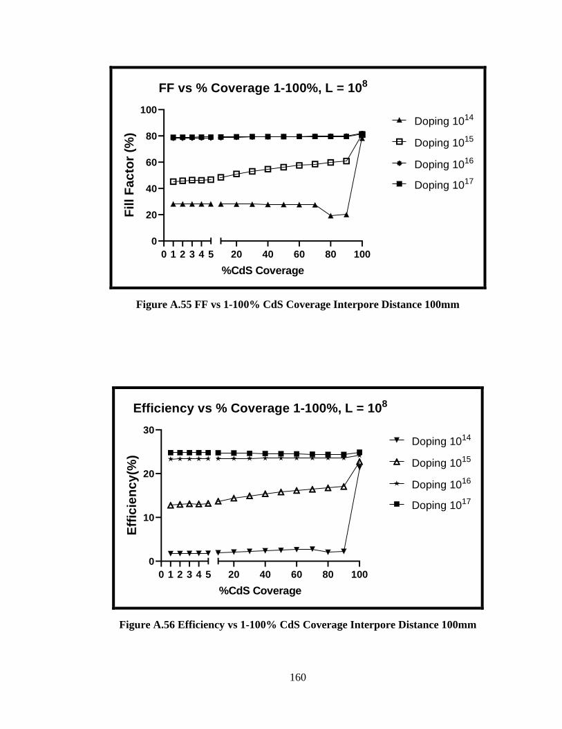
160
0 1 2 3 4 5
0
20
40
60
80
100
20 40 60 80 100
FF vs % Coverage 1-100%, L = 108
%CdS Coverage
Fill
Fa
cto
r (%
)Doping 1014
Doping 1015
Doping 1016
Doping 1017
Figure A.55 FF vs 1-100% CdS Coverage Interpore Distance 100mm
0 1 2 3 4 5
0
10
20
30
20 40 60 80 100
Efficiency vs % Coverage 1-100%, L = 108
%CdS Coverage
Eff
icie
nc
y(%
)
Doping 1014
Doping 1015
Doping 1016
Doping 1017
Figure A.56 Efficiency vs 1-100% CdS Coverage Interpore Distance 100mm

161
REFERENCES
[1]. D. M. Chapin, C.S.F., and G. L. Pearson, A New Silicon p-n Junction Photocell for
Converting Solar Radiation into Electrical Power. J. Appl. Phys., 1954. 25: p. 676.
[2]. D. C. Reynolds, G.L., L. L. Antes, and R. E. Marburger, Photovoltaic Effect in
Cadmium Sulfide. Phys. Rev., 1954. 96: p. 533.
[3]. Climate Central. world-passes-400-ppm-threshold-permanently, 2016.
[4]. Paul Denholm and Robert M Margolis. Land-use requirements and the per-capita
solar footprint for photovoltaic generation in the united states. Energy Policy,
36(9):3531–3543, 2008.
[5]. Shayle Kann. The state of solar, May 2016. GreenTech Media.
[6]. Michael Woodhouse, Rebecca Jones-Albertus, David Feldman, Ran Fu, Kelsey
Horowitz, Donald Chung, Dirk Jordan, and Sarah Kurtz. On the path to sunshot:
The role of advancements in solar photovoltaic efficiency, reliability, and costs.
Technical report, NREL (National Renewable Energy Laboratory), Golden, CO
(United States), 2016.
[7]. First Solar. First solar technology update, 2016.
[8]. On the path to sunshot: The role of advancements in solar photovoltaic efficiency,
reliability, and costs. Technical report, NREL (National Renewable Energy
Laboratory), Golden, CO (United States), 2016.
[9]. Antonio Luque and Steven Hegedus. Handbook of photovoltaic science and
engineering. John Wiley & Sons, 2011.
[10]. J Britt and C Ferekides. Thin-film CdS/CdTe solar cell with 15.8% efficiency.
Applied Physics Letters, 62(22):2851–2852, 1993.
162
[11]. First Solar. first solar global installation, 2015.
[12]. Khagendra P Bhandari, Jennifer M Collier, Randy J Ellingson, and Defne S Apul.
Energy payback time (epbt) and energy return on energy invested (eroi) of solar
photovoltaic systems: A systematic review and meta-analysis. Renewable and
Sustainable Energy Reviews, 47:133–141, 2015.
[13]. J. J. Loferski, "Theoretical Considerations Governing the Choice of the Optimum
Semiconductor for Photovoltaic Solar Energy Conversion," Journal of Applied
Physics, vol. 27, no. 7, pp. 777-784, 1956.
[14]. H. M. Dang, V. P. Singh, S. Guduru, and J. T. Hastings, “Embedded Nanowire
Window Layers for Enhancing Quantum Efficiency in Window-Absorber type
solar cells”, Solar Energy Materials and Solar Cells, 144 (2016) 641-651.
[15] J. M. Burst et al, “CdTe solar cells with open circuit voltage breaking the 1 V
barrier”, Nature Energy 1, 16015 (2016), March 2016.
[16]. K. Ernst, A. Belaidi, R. Konenkamp 18 (2003) 475-479.
[17]. R. Konenkamp , L. Dloczik, K. Ernst and C. Olesch, Physica E, 14,(2002) 219-23.
[18]. M. Green, Solid-State Electron.1981, 24, 788.
[19]. S.M. Sze, K. K. N., “Physics of semiconductor devices” (2007).
[20]. Tighineanu, A.; Ruff, T.; Albu, S.; Hahn, R.; Schmuki, P. Conductivity of TiO2
nanotubes: Influence of annealing time and temperature. Chem. Phys. Lett. 2010,
494, 260–263.
[21]. A.W. Czandema, C.N.R. Rao, J.M. Honig, Trans. Faraday Soc. 54 (1958) 1069.
163
[22]. L. Forro, O. Chauvet, D. Emin, L. Zuppiroli, H. Berger, F. Levy, J. Appl. Phys.
75(1993) 633.
[23] V. Zwilling, M. Aucouturier, E. Darque-Ceretti Anodic oxidation of titanium and
TA6V alloy in chromic media. An electrochemical approach Electrochim. Acta, 45
(1999), pp. 921-929.
[24] Zhao J, Wang X, Chen R et al (2005) Fabrication of Titanium oxide nanotubes
arrays by anodic oxidation. Solid State Commun 134: 705-710.
[25] O’Sullivan, J. P; Wood G. C. Proc. R. Soc. London, ser. A 1970, 317, 511.
[26] Roy P, Berger S, Schmuki P (2011) TiO2 nanotubes: synthesis and applications.
Angew Chem Int Ed 50(13):2904-2939.
[27] Macak JM, Tsuchiya H, Ghicov A et al (2007) TiO2 nanotubes: self-organized
electrochemical formation, properties and applications. Curr Opinion Solid State
Matter Sci 11 (1-2): 3-18.
[28]. Gong D, Grimes CA, Varghese OK et al (2001) Titanium oxide nanotube arrays
prepared by anodic oxidation. J Mater Res 16(12):3331–3334.
[29]. Mor GK, Varghese OK, Paulose M et al (2003) Fabrication of tapered, conical
shaped titania nanotubes. J Mater Res 18(11):2588–2593.
[30]. Varghese OK, Gong D, Paulose M et al (2003) Extreme changes in the electrical
resistance of titania nanotubes with hydrogen exposure. Adv Mater 15(7–8):624–
627.

164
[31]. Cai Q, Paulose M, Varghese OK et al (2005) The effect of electrolyte composition
on the fabrication of self-organized titanium oxide nanotube arrays by
anodic oxidation. J Mater Res 20(1):230–236.
[32]. Paulose M, Prakasam HE, Varghese OK et al (2007) TiO2 nanotube arrays of 1000
µm length by anodization of titanium foil: phenol red diffusion. J Phys Chem C
111(41):14992–14997.
[33]. Albu SP, Ghicov A, Aldabergenova S et al (2008) Formation of double walled TiO2
nanotubes and robust Anatase membranes. Adv Mater 20(21): 4135–4139.
[34]. N. K. Allam and C. A. Grimes, J. Phys. Chem. C, 2007, 111, 13028–13032.
[35]. N. K. Allam, K. Shankar and C. A. Grimes, J. Mater. Chem., 2008, 18, 2341–2346.
[36]. X. Chen, M. Schriver, T. Suen and S. S. Mao, Thin Solid Films, 2007, 515, 8511–
8514.
[37]. J. P. Frayret, R. Pointeau and A. Caprani, Electrochim. Acta, 1981, 26, 1783–1788.
[38]. Paulose M, Shankar K, Yoriya S et al (2006) Anodic growth of highly ordered TiO2
nanotube arrays to 134 μm in length. J Phys Chem B 110(33):16179–16184.
[39]. Raja KS, Gandhi T, Misra M (2007) Effect of water content of ethylene glycol as
electrolyte for synthesis of ordered titania nanotubes. Electrochem Commun
9(5):1069–1076.
[40]. Tsui, L.-k.; Zangari, G., Water content in the anodization electrolyte affects
the electrochemical and electronic transport properties of TiO2 nanotubes:

165
a study by electrochemical impedance spectroscopy. Electrochimica Acta,
2014, 121, 203-209.
[41]. Lockman Z, Sreekantan S, Ismail S et al (2010) Influence of anodisation voltage
on the dimension of titania nanotubes. J Alloys Compd 503(2):359–364.
[42]. Y. Alivov, M. Pandikunta, S. Nikishin, and Z. Fan, "The anodization voltage
influence on the properties of TiO2 nanotubes grown by electrochemical
oxidation," Nanotechnology, vol. 20, no. 22, p. 225602, 2009.
[43]. Allam NK, Grimes CA (2008) Effect of cathode material on the morphology and
photoelectrochemical properties of vertically oriented TiO2nanotube arrays. Solar
Energy Mater Solar Cells92:1468–1475.
[44]. Sreekantan S, Saharudin KA, Wei LC (2011) Formation of TiO2nanotubes via
anodization and potential applications for photo-catalysts, biomedical materials,
and photoelectrochemical cell.IOP Conf Series: Mater Sci Eng 21:012002.
doi:10.1088/1757-899X/21/1/012002.
[45]. P. Roy, S. Berger, P. Schmuki, TiO2nanotubes: synthesis and applications,
Angew.Chem. Int. Ed. 50 (2011) 2904.
[46]. Chu, S. Z.; Wada, K.; Inoue, S.; Isogai, M.; Yasumori, A. AdV.Mater. 2005, 17,
2115-2119.
[47]. R. V. Chernozem, M. A. Surmeneva, and R. A. Surmenev, “Influence of
anodization time and voltage on the parameters of TiO2 nanotubes,” IOP

166
Conference Series: Materials Science and Engineering, vol. 116, Article ID
012025, 2016.
[48]. Watcharenwong, A., Chanmanee, W., de Tacconi, N.R., Chenthamarakshan, C.R.,
Kajitvichyanukul, P. and Rajeshwar, K. (2007). Self–organized TiO2 nanotube
arrays by anodization of Ti substrate: Effect of anodization time, voltage and
medium composition on oxide morphology and photoelectrochemical response. J.
Mater Res., 22(11): 3186–95.
[49]. Wang J, Lin Z (2009) Anodic formation of ordered TiO2 nanotube arrays: effects
of electrolyte temperature and anodization potential. J Phys Chem C 113(10):4026–
4030.
[50]. Sulka GD, Kapusta-Kołodziej J, Brzózka A et al (2013) Anodic growth of TiO2
nanopore arrays at various temperatures. Electrochim Acta 104:526–535.
[51]. Sulka GD, Kapusta-Kołodziej J, Brzózka A et al (2013) Anodic growth of TiO2
nanopore arrays at various temperatures. Electrochim Acta 104:526–535.
[52]. Sun KC, Chen YC, Kuo MY et al (2011) Synthesis and characterization of highly
ordered TiO2 nanotube arrays for hydrogen generation via water splitting. Mater
Chem Phys 129:35–39.
[53]. Cai Q, Paulose M, Varghese OK et al (2005) The effect of electrolyte composition
on the fabrication of self-organized titanium oxide nanotube arrays by anodic
oxidation. J Mater Res 20(1):230–236.

167
[54]. SCAPS Manual
https://users.elis.ugent.be/ELISgroups/solar/projects/scaps/SCAPS%20manual%2
0most%20recent.pdf
[55]. H.J. Pauwels, G. Vanhoutte, Influence of interface states and energy barriers on
efficiency of heterojunction solar-cells, J. Phys. D-Appl. Phys., 11 (1978) 649-667.
[56]. H. Sopha, L. Hromadko, K. Nechvilova, J.M. Macak; Effect of electrolyte age and
potential changes on the morphology of TiO2 nanotubes J. Electroanal. Chem., 759
(2015), pp. 122-128.
[57]. Vahabzadeh, P.J., Gilani, N., Ebrahimian, P.A.: The effect of the anodization
voltage on the geometrical characteristics and photocatalytic activity of TiO2
nanotube arrays. Nano Struct Nano Objects 8, 7–14 (2016).
[58]. H. Dang, V. P. Singh, S. Guduru, J. Bowie, D. Cambron, "Electro optical
characterization of n-CdS nanowires/p-CdTe heterojunction solar cell devices",
2014 IEEE 40th Photovoltaic Specialist Conference (PVSC); IEEE, pp. 1601-1606,
2014.
[59]. H.M. Dang, Vijay Singh, Suresh Rajaputra, Sai Guduru, Sai Guduru, Jianhao Chen,
Bhavananda Nadimpally, "Cadmium sulfide nanowire arrays for window layer
applications in solar cells", Solar Energy Materials and Solar Cells, 26, 184-191,
2014.
[60]. V.P. Singh, D.L. Linam, D.W. Dils, J.C. McClure, G.B. Lush, "Electro-optical
characterization and modeling of thin film CdS-CdTe heterojunction solar cells",
Solar Energy Materials and Solar Cells, Vol. 63, pp 445-466, 2000.

168
[61]. Press Release, First Solar, 26 July 2011.
[62]. Press Release, First Solar, Feb 2016.

169
VITA
Deepak Kumar was born in Jamshedpur, India. He earned his bachelor’s degree
in Electronics Engineering in 2013 from Birsa Institute of Technology, Sindri, India. He
got enrolled for the Master of Science Program in electrical engineering at the University
of Kentucky in Fall 2017. He, during this program, worked as a researcher in the field of
nanotechnology on enhancinging the performance of nanostructured CdS- CdTe solar
cells.
Deepak Kumar