inverting voltage doubler
TRANSCRIPT
2002 Microchip Technology Inc. DS21453B-page 1
M TC682
Features
• 99.9% Voltage Conversion Efficiency
• 92% Power Conversion Efficiency• Wide Input Voltage Range
- +2.4V to +5.5V
• Only 3 External Capacitors Required• 185µA Supply Current• Space-Saving 8-Pin SOIC and 8-Pin PDIP
Packages
Applications
• -10V from +5V Logic Supply• -6V from a Single 3V Lithium Cell
• Portable Handheld Instruments• Cellular Phones• LCD Display Bias Generator
• Panel Meters• Operational Amplifier Power Supplies
Device Selection Table
General Description
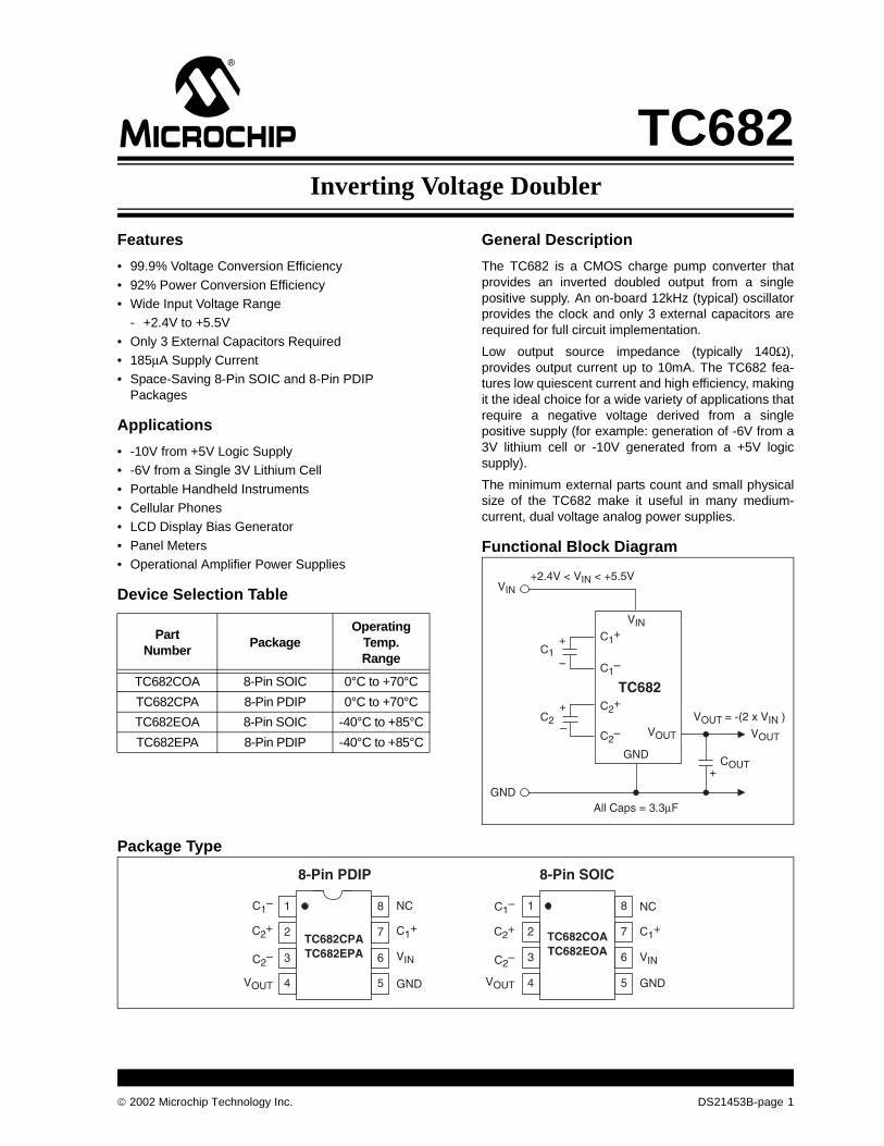
The TC682 is a CMOS charge pump converter thatprovides an inverted doubled output from a singlepositive supply. An on-board 12kHz (typical) oscillatorprovides the clock and only 3 external capacitors arerequired for full circuit implementation.
Low output source impedance (typically 140Ω),provides output current up to 10mA. The TC682 fea-tures low quiescent current and high efficiency, makingit the ideal choice for a wide variety of applications thatrequire a negative voltage derived from a singlepositive supply (for example: generation of -6V from a3V lithium cell or -10V generated from a +5V logicsupply).
The minimum external parts count and small physicalsize of the TC682 make it useful in many medium-current, dual voltage analog power supplies.
Functional Block Diagram
Package Type
PartNumber
PackageOperating
Temp.Range
TC682COA 8-Pin SOIC 0°C to +70°C
TC682CPA 8-Pin PDIP 0°C to +70°C
TC682EOA 8-Pin SOIC -40°C to +85°C
TC682EPA 8-Pin PDIP -40°C to +85°CGND
+
–
+
–
+
GND
VIN
VOUT = -(2 x VIN )
All Caps = 3.3µF
TC682
+2.4V < VIN < +5.5V
VOUT
C1+
VIN
C2+
C1–
C2–
COUT
VOUT
C1
C2
1
2
3
4
8
7
6
5
TC682CPATC682EPA
NC
GNDVOUT
C1+
1
2
3
4
8
7
6
5
TC682COATC682EOA
8-Pin PDIP 8-Pin SOIC
VIN
C2+
C1–
C2–
NC
GNDVOUT
C1+
VIN
C2+
C1–
C2–
Inverting Voltage Doubler

TC682
DS21453B-page 2 2002 Microchip Technology Inc.
1.0 ELECTRICAL CHARACTERISTICS
Absolute Maximum Ratings*
VIN .......................................................................+5.8VVIN dV/dT ........................................................ 1V/µsecVOUT ................................................................... -11.6V
Short-Circuit Duration - VOUT .....................ContinuousPower Dissipation (TA ≤ 70°C) 8-Pin PDIP ...............................................730mW 8-Pin SOIC ...............................................470mW
Operating Temperature Range............. -40°C to +85°CStorage Temperature (Unbiased) .......-65°C to +150°C
*Stresses above those listed under "Absolute MaximumRatings" may cause permanent damage to the device. Theseare stress ratings only and functional operation of the deviceat these or any other conditions above those indicated in theoperation sections of the specifications is not implied.Exposure to Absolute Maximum Rating conditions forextended periods may affect device reliability.
TC682 ELECTRICAL SPECIFICATIONS
Electrical Characteristics: Over operating temperature range, VIN = +5V, test circuit Figure 3-1 unless otherwise noted.
Symbol Parameter Min Typ Max Units Test Conditions
VIN Supply Voltage Range 2.4 — 5.5 V RL = 2kΩ
IIN Supply Current ——
185—
300400
µA RL = ∞, TA = 25°CRL = ∞
ROUT VOUT Source Resistance ——
140—
170
180230320
Ω IL– = 10mA, TA = 25°C
IL– = 10mA
IL– = 5mA, VIN = 2.8V
FOSC Oscillator Frequency — 12 — kHz
PEFF Power Efficiency 90 92 — % RL = 2kΩ, TA = 25°C
VOUTEFF Voltage Conversion Efficiency 99 99.9 — % VOUT, RL = ∞

2002 Microchip Technology Inc. DS21453B-page 3
TC682
2.0 PIN DESCRIPTION
The descriptions of the pins are listed in Table 2-1.
TABLE 2-1: PIN FUNCTION TABLE
Pin No.(8-Pin PDIP,
SOIC)Symbol Description
1 C1– Input. Capacitor C1 negative terminal.
2 C2+ Input. Capacitor C2 positive terminal.
3 C2– Input. Capacitor C2 negative terminal.
4 VOUT Output. Negative output voltage (-2VIN).
5 GND Input. Ground.
6 VIN Input. Power supply voltage.
7 C1+ Input. Capacitor C1 positive terminal.
8 NC No connection.

TC682
DS21453B-page 4 2002 Microchip Technology Inc.
3.0 DETAILED DESCRIPTION
FIGURE 3-1: TC682 TEST CIRCUIT
3.1 Phase 1
VSS charge storage – before this phase of the clockcycle, capacitor C1 is already charged to +5V. C1
+ isthen switched to ground and the charge in C1
– istransferred to C2
–. Since C2+ is at +5V, the voltage
potential across capacitor C2 is now -10V.
FIGURE 3-2: CHARGE PUMP – PHASE 1
3.2 Phase 2
VSS transfer – phase two of the clock connects the neg-ative terminal of C2 to the negative side of reservoircapacitor C3 and the positive terminal of C2 to ground,transferring the generated -10V to C3. Simultaneously,the positive side of capacitor C1 is switched to +5V andthe negative side is connected to ground. C2 is thenswitched to VCC and GND and Phase 1 begins again.
FIGURE 3-3: CHARGE PUMP – PHASE 2
3.3 Maximum Operating Limits
The TC682 has on-chip zener diodes that clamp VINto approximately 5.8V, and VOUT to -11.6V. Neverexceed the maximum supply voltage or excessivecurrent will be shunted by these diodes, potentiallydamaging the chip. The TC682 will operate over theentire operating temperature range with an inputvoltage of 2V to 5.5V.
3.4 Efficiency Considerations
Theoretically a charge pump voltage multiplier canapproach 100% efficiency under the followingconditions:
• The charge pump switches have virtually no offset and are extremely low on resistance.
• Minimal power is consumed by the drive circuitry.• The impedances of the reservoir and pump
capacitors are negligible.
For the TC682, efficiency is as shown below:
Voltage Efficiency = VOUT / (-2VIN)VOUT = -2VIN + VDROPVDROP = (IOUT) (ROUT)
Power Loss = IOUT (VDROP)
There will be a substantial voltage difference betweenVOUT and -2VIN if the impedances of the pump capaci-tors C1 and C2 are high with respect to their respectiveoutput loads.
Larger values of reservoir capacitor C3 will reduceoutput ripple. Larger values of both pump and reservoircapacitors improve the efficiency. See Section 4.2“Capacitor Selection”.
(+5V) 6
7
1
2
3
5
4
RLGND
+
–
+
–
+
GND
VIN
All Caps = 3.3µF
TC682
VOUT
C1+
VIN
C2+
C1–
C2–
COUT
V–OUT
C1
C2
–
VIN = +5V
VOUT
-5V
SW4
SW1
SW2
SW3
C2
C3
C1+
–
+
+
– –
+5V
VOUT
-10V
SW4SW2
SW1 SW3
C2
C3
C1+
–
+
+
– –

2002 Microchip Technology Inc. DS21453B-page 5
TC682
4.0 TYPICAL APPLICATIONS
4.1 Negative Doubling Converter
The most common application of the TC682 is as acharge pump voltage converter which provides anegative output of two times a positive input voltage(Figure 4-1).
FIGURE 4-1: INVERTING VOLTAGE DOUBLER
4.2 Capacitor Selection
The output resistance of the TC682 is determined, inpart, by the ESR of the capacitors used. An expressionfor ROUT is derived as shown below:
Assuming all switch resistances are approximatelyequal:
ROUT is typically 140Ω at +25°C with VIN = +5V and3.3µF low ESR capacitors. The fixed term (16RSW) isabout 80-90Ω. It can be seen easily that increasing ordecreasing values of C1 and C2 will affect efficiency bychanging ROUT. However, be careful about ESR. Thisterm can quickly become dominant with large electro-lytic capacitors. Table 4-1 shows ROUT for variousvalues of C1 and C2 (assume 0.5Ω ESR). C1 must berated at 6VDC or greater while C2 and C3 must berated at 12VDC or greater.
Output voltage ripple is affected by C3. Typically thelarger the value of C3 the less the ripple for a given loadcurrent. The formula for P-P VRIPPLE is given below:
VRIPPLE = 1/[2(fPUMP x C3)] + 2(ESRC3) (IOUT)
For a 10µF (0.5Ω ESR) capacitor for C3, fPUMP =10kHz and IOUT = 10mA the peak-to-peak ripple volt-age at the output will be less then 60mV. In mostapplications (IOUT < = 10mA) a 10-20µF capacitor and1-5µF pump capacitors will suffice. Table 4-2 showsVRIPPLE for different values of C3 (assume 1Ω ESR).
TABLE 4-1: OUTPUT RESISTANCEVS. C1, C2
TABLE 4-2: VRIPPLE PEAK-TO-PEAKVS. C3 (IOUT 10mA)
GND GND
TC682
22µF
22µF
22µF
7
6
54
3
2
1
+
VIN
C1+C2+
C1–
C2–
V–OUT
1
2
V–OUT
+
+
VIN
C3
ROUT = 2(RSW1 + RSW2 + ESRC1 + RSW3 + RSW4 + ESRC2)+2(RSW1 + RSW2 + ESRC1 + RSW3 + RSW4 + ESRC2)+1/(fPUMP x C1) +1/(fPUMP x C2)+ESRC3
ROUT = 16RSW + 4ESRC1 + 4ESRC2 + ESRC3+1/(fPUMP x C1) +1/(fPUMP x C2)
C1, C2 (µF) ROUT(Ω)
0.05 4085
0.10 2084
0.47 510
1.00 285
3.30 145
5.00 125
10.00 105
22.00 94
100.00 87
C3 (µF) VRIPPLE (mV)
0.50 1020
1.00 520
3.30 172
5.00 120
10.00 70
22.00 43
100.00 25

TC682
DS21453B-page 6 2002 Microchip Technology Inc.
4.3 Paralleling Devices
Paralleling multiple TC682s reduces the outputresistance of the converter. The effective outputresistance is the output resistance of a single devicedivided by the number of devices. As illustrated inFigure 4-2, each requires separate pump capacitors C1and C2, but all can share a single reservoir capacitor.
4.4 -5V Regulated Supply From A Single 3V Battery
Figure 4-3 shows a -5V power supply using one 3Vbattery. The TC682 provides -6V at VOUT, which isregulated to -5V by the negative LDO. The input to theTC682 can vary from 3V to 5.5V without affectingregulation appreciably. A TC54 device is connected tothe battery to detect undervoltage. This unit is set todetect at 2.7V. With higher input voltage, more currentcan be drawn from the outputs of the TC682. With 5Vat VIN, 10mA can be drawn from the regulated output.Assuming 150Ω source resistance for the converter,with IL
–= 10mA, the charge pump will droop 1.5V.
FIGURE 4-2: PARALLELING TC682 FOR LOWER OUTPUT SOURCE RESISTANCE
FIGURE 4-3: NEGATIVE SUPPLY DERIVED FROM 3V BATTERY
10µF
10µF10µF
10µF
22µF
VIN
GND
GND
NegativeSupply
TC682 TC682
GND
+
–
+
–
+
–
+
–
+
–
VIN
C1+
C2+
C1–
C2–V–OUT
VINC1+
C2+
C1–
C2–
V–OUT
C–OUT
VSS
VSS
GND
TC6823V
Ground
-5 Supply
LOW BATTERY
Negative LDO Regulator
TC54VC2702Exx
1µF
+
–+
–
+
–
+
–
+
–10µF
22µF
10µF
VINC1+
C2+
C1–
C2–
VIN
VIN VOUT
VOUT
V–OUT
COUT–

2002 Microchip Technology Inc. DS21453B-page 7
TC682
5.0 TYPICAL CHARACTERISTICS
Circuit of Figure 3-1, C1 = C2 = COUT = 3.3µF, TA = 25°C unless otherwise noted.
Note: The graphs and tables provided following this note are a statistical summary based on a limited number ofsamples and are provided for informational purposes only. The performance characteristics listed herein arenot tested or guaranteed. In some graphs or tables, the data presented may be outside the specifiedoperating range (e.g., outside specified power supply range) and therefore outside the warranted range.
VIN (V)
240
220
200
180
140
160
120
1 2 3 4 5 6
OU
TP
UT
RE
SIS
TA
NC
E (
Ω)
Output Resistance vs. VIN
C1 – C3 = 3.3µF
VIN (V)
300
250
200
150
50
100
1 2 3 4 5 6
SU
PP
LY
CU
RR
EN
T (
µA)
Supply Current vs. VIN
NO LOAD
VIN = 5V
OUTPUT CURRENT (mA)
200
150
100
50
00 5 1510 20
OU
TP
UT
RIP
PL
E (
mV
PK
-PK
)
Output Ripple vs. Output Current
C3 = 100µF
C3 = 10µF
LOAD CURRENT (mA)
0 5 10 15
-7.5
-8.0
-8.5
-9.0
-9.5
-10.0
-10.5
VO
UT
(V
)
VOUT vs. Load Current
VIN = 5V
TEMPERATURE (°C)
-50 0 50 100
200
180
160
140
120
100
80
OU
TP
UT
SO
UR
CE
RE
SIS
TA
NC
E (
Ω)
Output Source Resistance vs. Temperature
VIN = 5VIOUT = 10mA

TC682
DS21453B-page 8 2002 Microchip Technology Inc.
6.0 PACKAGING INFORMATION
6.1 Package Marking Information
Package marking data not available at this time.
6.2 Package Dimensions
3° MIN.
PIN 1
.260 (6.60)
.240 (6.10)
.045 (1.14)
.030 (0.76).070 (1.78).040 (1.02)
.400 (10.16).348 (8.84)
.200 (5.08)
.140 (3.56)
.150 (3.81)
.115 (2.92)
.110 (2.79)
.090 (2.29).022 (0.56).015 (0.38)
.040 (1.02)
.020 (0.51) .015 (0.38).008 (0.20)
.310 (7.87)
.290 (7.37)
.400 (10.16).310 (7.87)
8-Pin Plastic DIP
Dimensions: inches (mm)
.050 (1.27) TYP.
8° MAX.
PIN 1
.244 (6.20)
.228 (5.79).157 (3.99).150 (3.81)
.197 (5.00)
.189 (4.80)
.020 (0.51)
.013 (0.33).010 (0.25).004 (0.10)
.069 (1.75)
.053 (1.35) .010 (0.25).007 (0.18)
.050 (1.27)
.016 (0.40)
.
8-Pin SOIC
Dimensions: inches (mm)

2002 Microchip Technology Inc. DS21453B-page9
TC682
Sales and Support
Data SheetsProducts supported by a preliminary Data Sheet may have an errata sheet describing minor operational differences and recom-mended workarounds. To determine if an errata sheet exists for a particular device, please contact one of the following:
1. Your local Microchip sales office2. The Microchip Corporate Literature Center U.S. FAX: (480) 792-72773. The Microchip Worldwide Site (www.microchip.com)
Please specify which device, revision of silicon and Data Sheet (include Literature #) you are using.
New Customer Notification SystemRegister on our web site (www.microchip.com/cn) to receive the most current information on our products.
TC682
DS21453B-page10 2002 Microchip Technology Inc.
NOTES:

2002 Microchip Technology Inc. DS21453B-page 11
TC682
Information contained in this publication regarding deviceapplications and the like is intended through suggestion onlyand may be superseded by updates. It is your responsibility toensure that your application meets with your specifications.No representation or warranty is given and no liability isassumed by Microchip Technology Incorporated with respectto the accuracy or use of such information, or infringement ofpatents or other intellectual property rights arising from suchuse or otherwise. Use of Microchip’s products as critical com-ponents in life support systems is not authorized except withexpress written approval by Microchip. No licenses are con-veyed, implicitly or otherwise, under any intellectual propertyrights.
Trademarks
The Microchip name and logo, the Microchip logo, FilterLab,KEELOQ, microID, MPLAB, PIC, PICmicro, PICMASTER,PICSTART, PRO MATE, SEEVAL and The Embedded ControlSolutions Company are registered trademarks of Microchip Tech-nology Incorporated in the U.S.A. and other countries.
dsPIC, ECONOMONITOR, FanSense, FlexROM, fuzzyLAB,In-Circuit Serial Programming, ICSP, ICEPIC, microPort,Migratable Memory, MPASM, MPLIB, MPLINK, MPSIM,MXDEV, PICC, PICDEM, PICDEM.net, rfPIC, Select Modeand Total Endurance are trademarks of Microchip TechnologyIncorporated in the U.S.A.
Serialized Quick Turn Programming (SQTP) is a service markof Microchip Technology Incorporated in the U.S.A.
All other trademarks mentioned herein are property of theirrespective companies.
© 2002, Microchip Technology Incorporated, Printed in theU.S.A., All Rights Reserved.
Printed on recycled paper.
Microchip received QS-9000 quality system certification for its worldwide headquarters, design and wafer fabrication facilities in Chandler and Tempe, Arizona in July 1999 and Mountain View, California in March 2002. The Company’s quality system processes and procedures are QS-9000 compliant for its PICmicro® 8-bit MCUs, KEELOQ® code hopping devices, Serial EEPROMs, microperipherals, non-volatile memory and analog products. In addition, Microchip’s quality system for the design and manufacture of development systems is ISO 9001 certified.
DS21453B-page 12 2002 Microchip Technology Inc.
MAMERICASCorporate Office2355 West Chandler Blvd.Chandler, AZ 85224-6199Tel: 480-792-7200 Fax: 480-792-7277Technical Support: 480-792-7627Web Address: http://www.microchip.comRocky Mountain2355 West Chandler Blvd.Chandler, AZ 85224-6199Tel: 480-792-7966 Fax: 480-792-7456
Atlanta500 Sugar Mill Road, Suite 200BAtlanta, GA 30350Tel: 770-640-0034 Fax: 770-640-0307Boston2 Lan Drive, Suite 120Westford, MA 01886Tel: 978-692-3848 Fax: 978-692-3821Chicago333 Pierce Road, Suite 180Itasca, IL 60143Tel: 630-285-0071 Fax: 630-285-0075Dallas4570 Westgrove Drive, Suite 160Addison, TX 75001Tel: 972-818-7423 Fax: 972-818-2924DetroitTri-Atria Office Building 32255 Northwestern Highway, Suite 190Farmington Hills, MI 48334Tel: 248-538-2250 Fax: 248-538-2260Kokomo2767 S. Albright Road Kokomo, Indiana 46902Tel: 765-864-8360 Fax: 765-864-8387Los Angeles18201 Von Karman, Suite 1090Irvine, CA 92612Tel: 949-263-1888 Fax: 949-263-1338New York150 Motor Parkway, Suite 202Hauppauge, NY 11788Tel: 631-273-5305 Fax: 631-273-5335San JoseMicrochip Technology Inc.2107 North First Street, Suite 590San Jose, CA 95131Tel: 408-436-7950 Fax: 408-436-7955Toronto6285 Northam Drive, Suite 108Mississauga, Ontario L4V 1X5, CanadaTel: 905-673-0699 Fax: 905-673-6509
ASIA/PACIFICAustraliaMicrochip Technology Australia Pty LtdSuite 22, 41 Rawson StreetEpping 2121, NSWAustraliaTel: 61-2-9868-6733 Fax: 61-2-9868-6755China - BeijingMicrochip Technology Consulting (Shanghai)Co., Ltd., Beijing Liaison OfficeUnit 915Bei Hai Wan Tai Bldg.No. 6 Chaoyangmen Beidajie Beijing, 100027, No. ChinaTel: 86-10-85282100 Fax: 86-10-85282104China - ChengduMicrochip Technology Consulting (Shanghai)Co., Ltd., Chengdu Liaison OfficeRm. 2401, 24th Floor, Ming Xing Financial TowerNo. 88 TIDU StreetChengdu 610016, ChinaTel: 86-28-6766200 Fax: 86-28-6766599China - FuzhouMicrochip Technology Consulting (Shanghai)Co., Ltd., Fuzhou Liaison OfficeUnit 28F, World Trade PlazaNo. 71 Wusi RoadFuzhou 350001, ChinaTel: 86-591-7503506 Fax: 86-591-7503521China - ShanghaiMicrochip Technology Consulting (Shanghai)Co., Ltd.Room 701, Bldg. BFar East International PlazaNo. 317 Xian Xia RoadShanghai, 200051Tel: 86-21-6275-5700 Fax: 86-21-6275-5060China - ShenzhenMicrochip Technology Consulting (Shanghai)Co., Ltd., Shenzhen Liaison OfficeRm. 1315, 13/F, Shenzhen Kerry Centre,Renminnan LuShenzhen 518001, ChinaTel: 86-755-2350361 Fax: 86-755-2366086Hong KongMicrochip Technology Hongkong Ltd.Unit 901-6, Tower 2, Metroplaza223 Hing Fong RoadKwai Fong, N.T., Hong KongTel: 852-2401-1200 Fax: 852-2401-3431IndiaMicrochip Technology Inc.India Liaison OfficeDivyasree Chambers1 Floor, Wing A (A3/A4)No. 11, O’Shaugnessey RoadBangalore, 560 025, IndiaTel: 91-80-2290061 Fax: 91-80-2290062
JapanMicrochip Technology Japan K.K.Benex S-1 6F3-18-20, ShinyokohamaKohoku-Ku, Yokohama-shiKanagawa, 222-0033, JapanTel: 81-45-471- 6166 Fax: 81-45-471-6122KoreaMicrochip Technology Korea168-1, Youngbo Bldg. 3 FloorSamsung-Dong, Kangnam-KuSeoul, Korea 135-882Tel: 82-2-554-7200 Fax: 82-2-558-5934SingaporeMicrochip Technology Singapore Pte Ltd.200 Middle Road#07-02 Prime CentreSingapore, 188980Tel: 65-6334-8870 Fax: 65-6334-8850TaiwanMicrochip Technology Taiwan11F-3, No. 207Tung Hua North RoadTaipei, 105, TaiwanTel: 886-2-2717-7175 Fax: 886-2-2545-0139
EUROPEDenmarkMicrochip Technology Nordic ApSRegus Business CentreLautrup hoj 1-3Ballerup DK-2750 DenmarkTel: 45 4420 9895 Fax: 45 4420 9910FranceMicrochip Technology SARLParc d’Activite du Moulin de Massy43 Rue du Saule TrapuBatiment A - ler Etage91300 Massy, FranceTel: 33-1-69-53-63-20 Fax: 33-1-69-30-90-79GermanyMicrochip Technology GmbHGustav-Heinemann Ring 125D-81739 Munich, GermanyTel: 49-89-627-144 0 Fax: 49-89-627-144-44ItalyMicrochip Technology SRLCentro Direzionale Colleoni Palazzo Taurus 1 V. Le Colleoni 120041 Agrate BrianzaMilan, Italy Tel: 39-039-65791-1 Fax: 39-039-6899883United KingdomArizona Microchip Technology Ltd.505 Eskdale RoadWinnersh TriangleWokingham Berkshire, England RG41 5TUTel: 44 118 921 5869 Fax: 44-118 921-5820
03/01/02
WORLDWIDE SALES AND SERVICE