introduction to vhdl - michigan technological … labs/lab 2 - introduction to vhdl.pdflab 2 –...
TRANSCRIPT
Lab 2 Introduction to VHDL

2-1
Lab 2 – Introduction to VHDL
In this lab you will design, test, and simulate a basic logic circuit using the Quartus II development software. The circuit you will create is a ripple-carry four-bit adder/subtractor using both behavioral and structural VHDL coding. Below is a schematic diagram of the complete circuit. The component make-up includes four full adders and four XOR logic gates. The inputs are two four-bit numbers; A and B, and an add/subtract selection input; Sel. The outputs are four-bit sum; Sum, and a carry-out output; Cout.
Below is a detailed diagram of the full adder circuit used. It consists of three two-input AND gates, two XOR gates, and one three-input OR gate. The individual gates will be coded separately using behavioral style VHDL, and then stitched together using structural style VHDL to create the full adder.
AND2_0
AND2_1
AND2_2
XOR2_0
XOR2_1
OR3_1
A
B
Cin
XOR2_0_out
AND2_0_out
AND2_1_out
AND2_2_out
Sum
Cout

2-2
Task 1: Create a New Project
1. Start the Quartus II software. From the Windows Start Menu, select: All Programs → Other Apps → Altera → Quartus II 9.1 → Quartus II 9.1 (32-Bit)
2. Start the New Project Wizard. If the opening splash screen is displayed, select: Create a New Project (New Project Wizard), otherwise from the Quartus II Menu Bar select: File → New Project Wizard.
3. Select the Working Directory and Project Name.
Working Directory H:\Altera_Training\Lab2
Project Name Lab2
Top-Level Design Entity Lab2
Click Next to advance to page 2 of the New Project Wizard. Note: A window may pop up stating that the chosen working directory does not exist. Click Yes to create it.
2-3
4. Click Next again as we will not be adding any preexisting design files at this time.
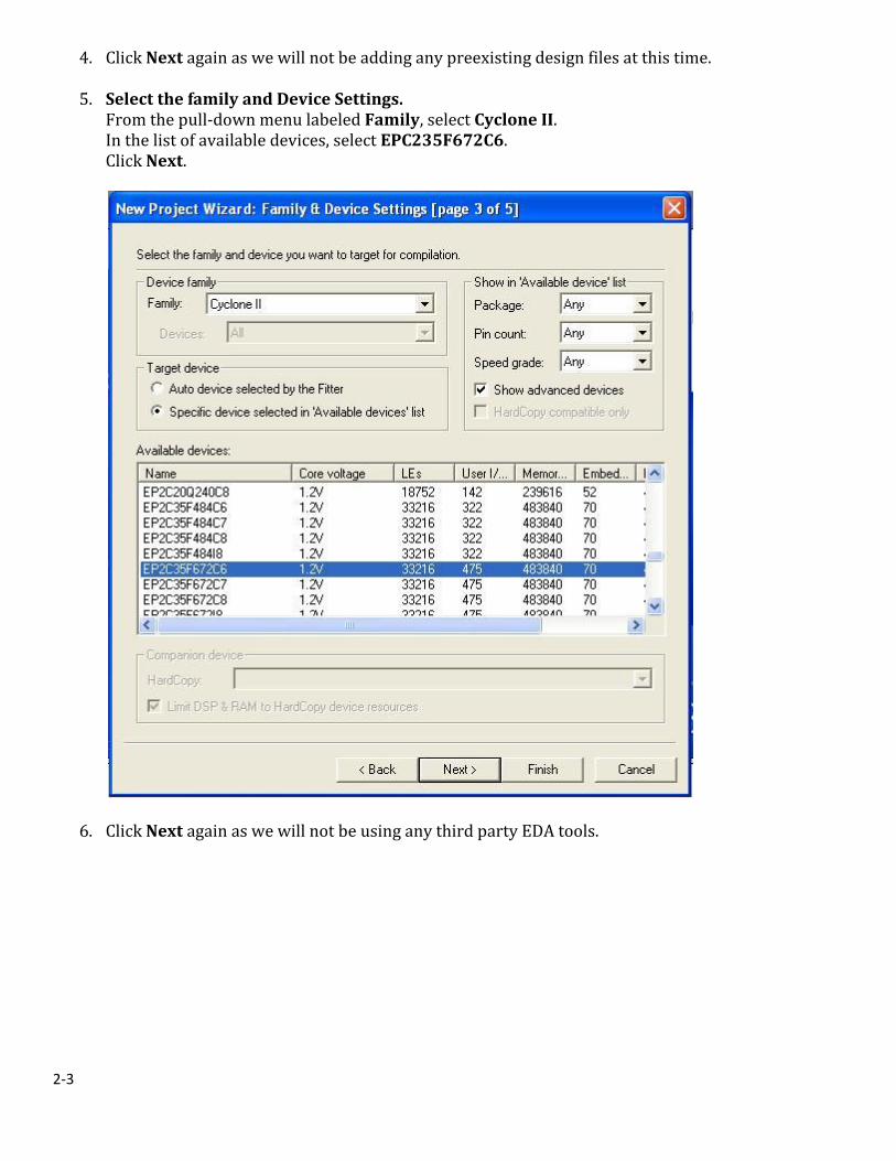
5. Select the family and Device Settings.
From the pull-down menu labeled Family, select Cyclone II. In the list of available devices, select EPC235F672C6. Click Next.
6. Click Next again as we will not be using any third party EDA tools.

2-4
7. Click Finish to complete the New Project Wizard.

2-5
Task 2: Create, Add, and Compile Design Files
1. Create a new Design File. Select: File → New from the Menu Bar. Select: VHDL File from the Design Files list and click OK.
2-6
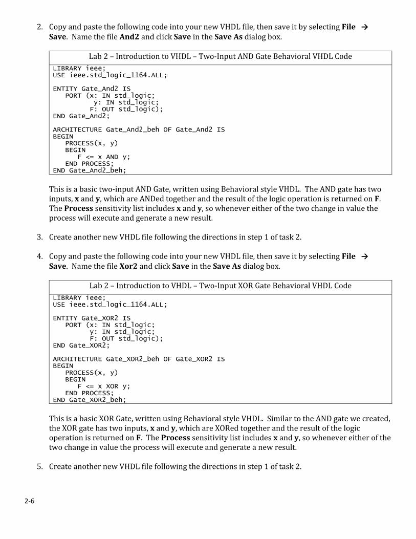
2. Copy and paste the following code into your new VHDL file, then save it by selecting File →
Save. Name the file And2 and click Save in the Save As dialog box.
Lab 2 – Introduction to VHDL – Two-Input AND Gate Behavioral VHDL Code
LIBRARY ieee; USE ieee.std_logic_1164.ALL; ENTITY Gate_And2 IS PORT (x: IN std_logic; y: IN std_logic; F: OUT std_logic); END Gate_And2; ARCHITECTURE Gate_And2_beh OF Gate_And2 IS BEGIN PROCESS(x, y) BEGIN F <= x AND y; END PROCESS; END Gate_And2_beh;
This is a basic two-input AND Gate, written using Behavioral style VHDL. The AND gate has two inputs, x and y, which are ANDed together and the result of the logic operation is returned on F. The Process sensitivity list includes x and y, so whenever either of the two change in value the process will execute and generate a new result.
3. Create another new VHDL file following the directions in step 1 of task 2.
4. Copy and paste the following code into your new VHDL file, then save it by selecting File → Save. Name the file Xor2 and click Save in the Save As dialog box.
Lab 2 – Introduction to VHDL – Two-Input XOR Gate Behavioral VHDL Code
LIBRARY ieee; USE ieee.std_logic_1164.ALL; ENTITY Gate_XOR2 IS PORT (x: IN std_logic; y: IN std_logic; F: OUT std_logic); END Gate_XOR2; ARCHITECTURE Gate_XOR2_beh OF Gate_XOR2 IS BEGIN PROCESS(x, y) BEGIN F <= x XOR y; END PROCESS; END Gate_XOR2_beh;
This is a basic XOR Gate, written using Behavioral style VHDL. Similar to the AND gate we created, the XOR gate has two inputs, x and y, which are XORed together and the result of the logic operation is returned on F. The Process sensitivity list includes x and y, so whenever either of the two change in value the process will execute and generate a new result.
5. Create another new VHDL file following the directions in step 1 of task 2.
2-7
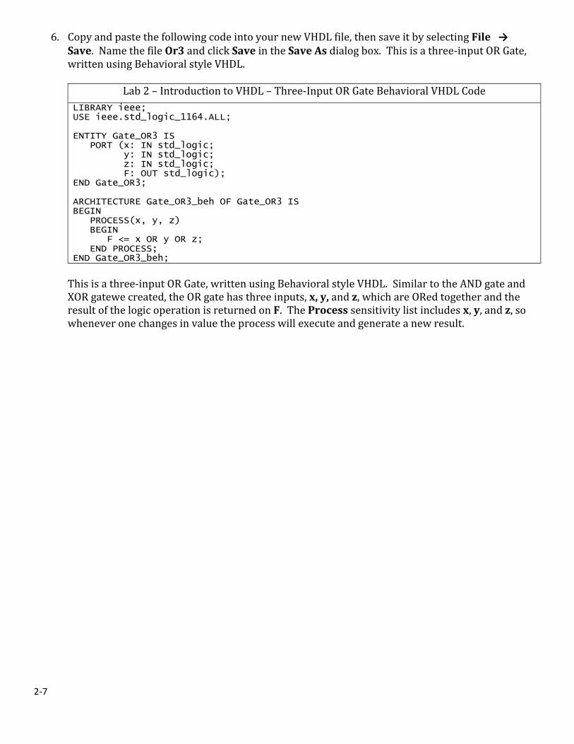
6. Copy and paste the following code into your new VHDL file, then save it by selecting File →
Save. Name the file Or3 and click Save in the Save As dialog box. This is a three-input OR Gate, written using Behavioral style VHDL.
Lab 2 – Introduction to VHDL – Three-Input OR Gate Behavioral VHDL Code
LIBRARY ieee; USE ieee.std_logic_1164.ALL; ENTITY Gate_OR3 IS PORT (x: IN std_logic; y: IN std_logic; z: IN std_logic; F: OUT std_logic); END Gate_OR3; ARCHITECTURE Gate_OR3_beh OF Gate_OR3 IS BEGIN PROCESS(x, y, z) BEGIN F <= x OR y OR z; END PROCESS; END Gate_OR3_beh;
This is a three-input OR Gate, written using Behavioral style VHDL. Similar to the AND gate and XOR gatewe created, the OR gate has three inputs, x, y, and z, which are ORed together and the result of the logic operation is returned on F. The Process sensitivity list includes x, y, and z, so whenever one changes in value the process will execute and generate a new result.
2-8
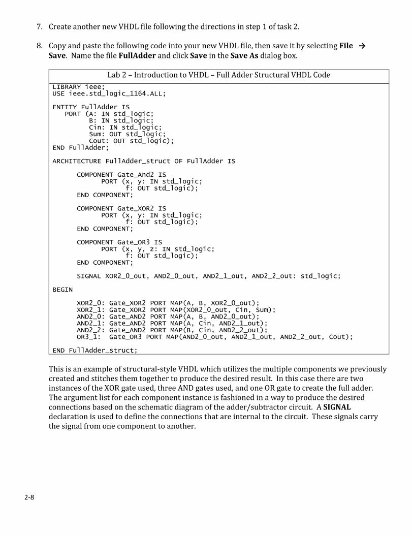
7. Create another new VHDL file following the directions in step 1 of task 2.
8. Copy and paste the following code into your new VHDL file, then save it by selecting File →
Save. Name the file FullAdder and click Save in the Save As dialog box.
Lab 2 – Introduction to VHDL – Full Adder Structural VHDL Code
LIBRARY ieee; USE ieee.std_logic_1164.ALL; ENTITY FullAdder IS PORT (A: IN std_logic; B: IN std_logic; Cin: IN std_logic; Sum: OUT std_logic; Cout: OUT std_logic); END FullAdder; ARCHITECTURE FullAdder_struct OF FullAdder IS COMPONENT Gate_And2 IS PORT (x, y: IN std_logic; f: OUT std_logic); END COMPONENT; COMPONENT Gate_XOR2 IS PORT (x, y: IN std_logic; f: OUT std_logic); END COMPONENT; COMPONENT Gate_OR3 IS PORT (x, y, z: IN std_logic; f: OUT std_logic); END COMPONENT; SIGNAL XOR2_0_out, AND2_0_out, AND2_1_out, AND2_2_out: std_logic; BEGIN XOR2_0: Gate_XOR2 PORT MAP(A, B, XOR2_0_out); XOR2_1: Gate_XOR2 PORT MAP(XOR2_0_out, Cin, Sum); AND2_0: Gate_AND2 PORT MAP(A, B, AND2_0_out); AND2_1: Gate_AND2 PORT MAP(A, Cin, AND2_1_out); AND2_2: Gate_AND2 PORT MAP(B, Cin, AND2_2_out); OR3_1: Gate_OR3 PORT MAP(AND2_0_out, AND2_1_out, AND2_2_out, Cout); END FullAdder_struct;
This is an example of structural-style VHDL which utilizes the multiple components we previously created and stitches them together to produce the desired result. In this case there are two instances of the XOR gate used, three AND gates used, and one OR gate to create the full adder. The argument list for each component instance is fashioned in a way to produce the desired connections based on the schematic diagram of the adder/subtractor circuit. A SIGNAL declaration is used to define the connections that are internal to the circuit. These signals carry the signal from one component to another.

2-9
9. Create another new VHDL file following the directions in step 1 of task 2.
10. Copy and paste the following code into your new VHDL file, then save it by selecting File → Save. Name the file Lab2 and click Save in the Save As dialog box. This is the Full Adder circuit, written using Structural style VHDL.
Lab 2 – Introduct on to VHDL – Adder/Subtractor Structural VHDL Code
LIBRARY ieee; USE ieee.std_logic_1164.ALL;
ENTITY Lab2 IS PORT (A: IN std_logic_vector(3 DOWNTO 0); B: IN std_logic_vector(3 DOWNTO 0); Sel: IN std_logic; Sum: OUT std_logic_vector(3 DOWNTO 0); Cout: OUT std_logic); END Lab2;
ARCHITECTURE AddSub_struct OF Lab2 IS
COMPONENT Gate_XOR2 IS PORT (x, y: IN std_logic; f: OUT std_logic); END COMPONENT; COMPONENT FullAdder IS PORT (A: IN std_logic; B: IN std_logic; Cin: IN std_logic; Sum: OUT std_logic; Cout: OUT std_logic); END COMPONENT; SIGNAL XOR2_0_out, XOR2_1_out, XOR2_2_out, XOR2_3_out: std_logic; SIGNAL c1, c2, c3: std_logic; BEGIN XOR2_0: Gate_XOR2 PORT MAP(B(0), Sel, XOR2_0_out); XOR2_1: Gate_XOR2 PORT MAP(B(1), Sel, XOR2_1_out); XOR2_2: Gate_XOR2 PORT MAP(B(2), Sel, XOR2_2_out); XOR2_3: Gate_XOR2 PORT MAP(B(3), Sel, XOR2_3_out); FullAdder_0: FullAdder PORT MAP(A(0), XOR2_0_out, Sel, Sum(0), c1); FullAdder_1: FullAdder PORT MAP(A(1), XOR2_1_out, c1, Sum(1), c2); FullAdder_2: FullAdder PORT MAP(A(2), XOR2_2_out, c2, Sum(2), c3); FullAdder_3: FullAdder PORT MAP(A(3), XOR2_3_out, c3, Sum(3), Cout); END AddSub_struct;
11. Compile the design by clicking the Start Compilation button on the Toolbar.

2-10
Task 3: Simulate Design using Quartus II
1. Create a Vector Waveform File (vwf)
Click the New File icon on the Menu Bar Select Vector Waveform File under the Verification/Debugging Files heading.
2. Add Signals to the Waveform Select Edit → Insert → Insert Node or Bus… to open the Insert Node or Bus window.
2-11
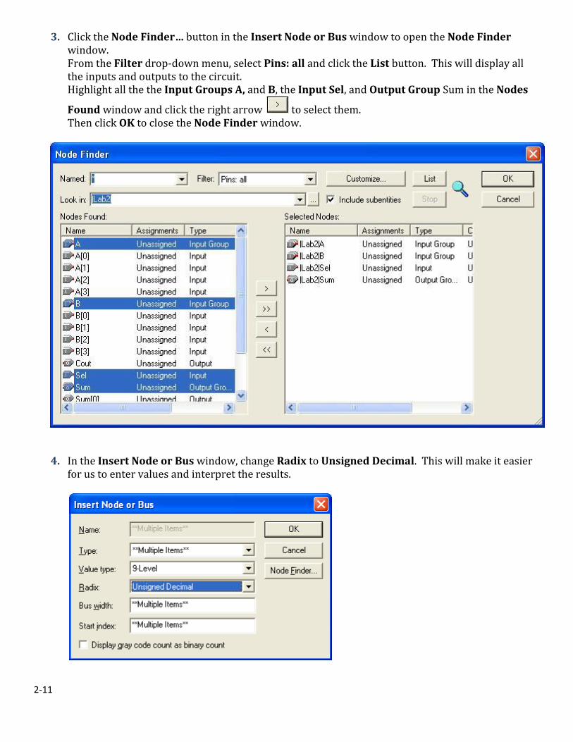
3. Click the Node Finder… button in the Insert Node or Bus window to open the Node Finder
window. From the Filter drop-down menu, select Pins: all and click the List button. This will display all the inputs and outputs to the circuit. Highlight all the the Input Groups A, and B, the Input Sel, and Output Group Sum in the Nodes
Found window and click the right arrow to select them. Then click OK to close the Node Finder window.
4. In the Insert Node or Bus window, change Radix to Unsigned Decimal. This will make it easier for us to enter values and interpret the results.
2-12
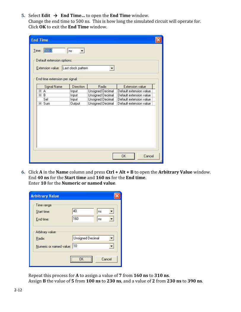
5. Select Edit → End Time… to open the End Time window.
Change the end time to 500 ns. This is how long the simulated circuit will operate for. Click OK to exit the End Time window.
6. Click A in the Name column and press Ctrl + Alt + B to open the Arbitrary Value window. End 40 ns for the Start time and 160 ns for the End time. Enter 10 for the Numeric or named value.
Repeat this process for A to assign a value of 7 from 160 ns to 310 ns. Assign B the value of 5 from 100 ns to 230 ns, and a value of 2 from 230 ns to 390 ns.

2-13
On the waveform row for Sel, click and drag to highlight the waveform from 130 ns to 200 ns. Press Ctrl + Alt + 1 to assign this section of the waveform a value of 1. Repeat this process for the value of Sel from 270 ns to 350 ns.
After completing the signal assignments the waveform graph should look similar to the image below:
Leave Sum with a value of undefined (X), as values for this will be generated when the simulation runs.
Click the Save icon on the Menu bar and save the vwf file with the filename Lab2.vwf.

2-14
7. From the Toolbar, select Assignments → Settings to open the Settings window.
Click the Simulator Settings heading and set Simulation Mode to Functional.
Simulation input should be the name of your vwf file, Lab2.vwf. If not, click the ellipses and select Lab2.vwf. Click OK to save the changes and close the Settings window.
8. Click the Start Compilation button on the Menu bar to compile the design. Ignore any warnings generated.
9. Select Processing → Generate Functional Simulation Netlist and click OK when it has completed.
10. Run the simulation by clicking the Start Simulation button on the Toolbar. Click OK once the simulator has completed.

2-15
11. The output waveforms for Cout and Sum should look similar to the screen capture below;
When Sel is low, A is added to B and the result is displayed as the value of Sum. When Sel is high, B is subtracted from A and Sum is the result.
12. Change the simulation mode to Timing by selecting Assignments → Settings to open the Settings window. Click the Simulator Settings heading and set Simulation Mode to Timing.
13. Click the Start Simulation button and observe the change in the output waveforms for Cout and Sum. In Timing mode the simulator uses estimated or actual timing information to test the logical operation and the timing of your design.
Task 4: Implementing the Design on the DE2 Board
1. From the Menu Bar select: Assignments → Assignment Editor
2. From the drop-down menu at the top, for Category, select Pin.
2-16
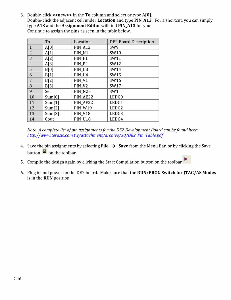
3. Double-click <<new>> in the To column and select or type A[0].
Double-click the adjacent cell under Location and type PIN_A13. For a shortcut, you can simply type A13 and the Assignment Editor will find PIN_A13 for you. Continue to assign the pins as seen in the table below.
To Location DE2 Board Description 1 A[0] PIN_A13 SW9 2 A[1] PIN_N1 SW10 3 A[2] PIN_P1 SW11 4 A[3] PIN_P2 SW12 5 B[0] PIN_U3 SW14 6 B[1] PIN_U4 SW15 7 B[2] PIN_V1 SW16 8 B[3] PIN_V2 SW17 9 Sel PIN_N25 SW1 10 Sum[0] PIN_AE22 LEDG0 11 Sum[1] PIN_AF22 LEDG1 12 Sum[2] PIN_W19 LEDG2 13 Sum[3] PIN_V18 LEDG3 14 Cout PIN_U18 LEDG4
Note: A complete list of pin assignments for the DE2 Development Board can be found here: http://www.terasic.com.tw/attachment/archive/30/DE2_Pin_Table.pdf
4. Save the pin assignments by selecting File → Save from the Menu Bar, or by clicking the Save
button on the toolbar.
5. Compile the design again by clicking the Start Compilation button on the toolbar .
6. Plug in and power on the DE2 board. Make sure that the RUN/PROG Switch for JTAG/AS Modes is in the RUN position.
2-17
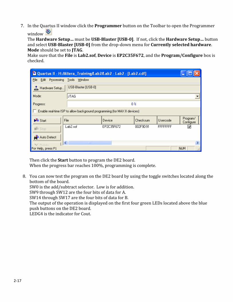
7. In the Quartus II window click the Programmer button on the Toolbar to open the Programmer
window The Hardware Setup… must be USB-Blaster [USB-0]. If not, click the Hardware Setup… button and select USB-Blaster [USB-0] from the drop-down menu for Currently selected hardware. Mode should be set to JTAG. Make sure that the File is Lab2.sof, Device is EP2C35F672, and the Program/Configure box is checked.
Then click the Start button to program the DE2 board. When the progress bar reaches 100%, programming is complete.
8. You can now test the program on the DE2 board by using the toggle switches located along the bottom of the board. SW0 is the add/subtract selector. Low is for addition. SW9 through SW12 are the four bits of data for A. SW14 through SW17 are the four bits of data for B. The output of the operation is displayed on the first four green LEDs located above the blue push buttons on the DE2 board. LEDG4 is the indicator for Cout.