integrated rf power amplifler design in silicon-based
TRANSCRIPT

Integrated RF Power AmplifierDesign in Silicon-Based
Technologies
Von der Fakultat fur Mathematik, Naturwissenschaften und Informatikder Brandenburgischen Technischen Universitat Cottbus
zur Erlangung des akademischen Grades
Doktor der Ingenieurwissenschaften(Dr.-Ing.)
genehmigte Dissertation
vorgelegt von
Magister
Andriy Vasylyev
geboren am 04.08.1977 in Wassylkiw (Ukraine)
Gutachter: Prof. Dr. Heinrich Klar (TU Berlin)
Gutachter: Prof. Dr. Georg Bock (TU Berlin)
Gutachter: Prof. Dr. Peter Weger (BTU Cottbus)
Tag der mundlichen Prufung: 17 Juli 2006

Acknowledgements
I would like to express sincere appreciation to my advisor Prof. Dr. Peter Wegerfor his guidance and support over this work.
I am also grateful to Volodymyr Slobodyanyuk, Oleksiy Gerasika, WojciechDebski and Valentyn Solomko from BTU Design Group(Chair of Circuit Design),Winfried Bakalski, Werner Simburger, Ronald Thuringer, Daniel Kehrer, MarcTiebout, Hans-Dieter Wohlmuth, Herbert Knapp and Mirjana Rest from INFI-NEON Technologies AG, Corporate Research, Department for High FrequencyCircuits, Munich for their informative discussions and help during this work.
Finally, I would like to take this opportunity to thank my wife Iryna, mydaughter Kateryna, my in-laws and my parents, my brother Sergey for theirvaluable support and indefatigable faith throughout my life.
The work presented is done within INTRINSYK research project which ispursued in cooperation with INFINEON Technologies AG, SIEMENS AG, andUniversity of Bochum.
ii
Abstract
This thesis presents the design and implementation of the RF power amplifiersin modern silicon based technologies. The main challenge is to include poweramplifier on a single chip with output power level in watts, operating at highfrequencies where the transit frequency (fT ) is just a few times higher than theoperating frequency.
This work describes the design procedure for bipolar and CMOS transformer-based Class-A, Class-AB and Class-B power amplifiers. The design procedure isbased on the HICUM for bipolar and BSIM4 for CMOS transistor models and isdivided in four parts:
• Building a one transistor prototype power amplifier which is based on theanalytical analysis of the output characteristics and transistor model.
• Load-pull simulation to define the final input and output impedances.
• Derivation of the analytical equations for the transformer-based matchingnetwork.
• Design of the final transformer-based push-pull power amplifier.
A good agreement between the proposed analytical analysis and large-signal(harmonic balance) simulation results proofs usefulness of the proposed poweramplifier design approach. Additionally, it shows the contribution of the separateddevices at the final design that helps to find a technology limits in the currentcircuit design.
The main achievements include:
• A 2.4 GHz power amplifier in 0.13 µm CMOS technology. An output powerof 28 dBm is achieved with a power added efficiency of 48 % at a supplyvoltage of 1.2 V [Vasylyev 04].
• Two 17 GHz power amplifiers in 0.13 µm CMOS technology (one fullyintegrated while the other with external matching network) with outputpower exceeding 50 mW. The former exhibits a power added efficiency of9.3 % while the latter a 15.6 % power added efficiency [Vasylyev 06].
• A fully integrated K and Ka bands power amplifier in 0.13 µm CMOStechnology. A 13 dBm output power along with power added efficiency
iii

iv
of 13 % is achieved at an operating frequency of 25.7 GHz with 1.2 Vsupply [Vasylyev 05,a].
• A fully integrated power amplifier based on a novel power combining trans-former structure in 28 GHz-fT SiGe-bipolar technology. A 32 dBm outputpower along with power added efficiency of 30 % is achieved at an operatingfrequency of 2.12 GHz with 3.5 V supply [Vasylyev 05,b].

Zusammenfassung
Diese Doktorarbeit beschaftigt sich mit dem Entwurf und der Ausfuhrung vonHochfrequenz-Leistungsverstarkern in modernen Silizium Technologien. Die Her-ausforderung ist, HF-Leistungsverstarker mit mehreren Watt Ausgangsleistungvollstandig monolithisch zu integrieren; wobei die Betriebsfrequenz bereits 25 %der Transitfrequenz (fT ) betragt.
Diese Arbeit beschreibt das Entwurfverfahren fur bipolar und CMOS Leis-tungsverstarker der Klasse-A, Klasse-AB und Klasse-B mit monolithisch integri-erten Transformatoren. Das Entwurfverfahren verwendet fur bipolar das HICUMTransistor-Modell und fur CMOS das BSIM4 Transistor-Modell und lasst sich invier Teile gliedern:
• Analyse eines Ein-Transistor-Verstarkers, basierend auf der analytischenAnalyse der Ausgangcharakteristiken und der Transistor-Modelle.
• Simulation mit Lastvariation, zur Ermittlung der optimalen Ein-und Aus-gangsimpedanzen.
• Ableitung der analytischen Gleichungen fur das Transformator Anpassungsnetz.
• Entwurf vom optimierten Gegentaktleistungsverstarker mit monolithischenTransformatoren.
Eine gute Ubereinstimmung zwischen der vorgeschlagenen analytischen Analy-se und dem Großsignal-Simulationenergebnis beweist die Nutzlichkeit der vorgeschla-genen Verstarker-Entwurfannaherung. Zusatzlich zeigt es den Beitrag der einzel-nen Komponenten, was das optimale Ausreizen der Technologie ermoglicht.
Die Hauptergebnisse:
• Ein 2.4 GHz Leistungsverstarker in einer 0.13 µm CMOS Technologie miteiner Ausgangsleistung von 28 dBm und einem Verstarkerwirkungsgrad von48 % an einer Versorgungsspannung von 1.2 V [Vasylyev 04].
• Zwei 17 GHz Leistungsverstarker in einer 0.13 µm CMOS Technologie (eineVariante enthalt ein monolithisch integriertes Anpassungsnetzwerk, die an-dere Variante enthalt ein externes Anpassungsnetzwerk) mit einer Aus-gangsleistung uber 50 mW. Der Verstarkerwirkungsgrad betragt 9.3 % furVariante 1 und 15.6 % fur Variante 2 [Vasylyev 06].
v

vi
• Ein vollig integrierter K und Ka Band-Leistungsverstarker in einer 0.13 µmCMOS Technologie. Bei einer Betriebsfrequenz von 25.7 GHz wird eineAusgangsleistung von 13 dBm und ein Verstarkerwirkungsgrad von 13 %erreicht (1.2 V Versorgungsspannung) [Vasylyev 05,a].
• Ein vollig integrierter Leistungsverstarker basierend auf einer neuartigenTransformator-Struktur in einer 28 GHz-fT SiGe Bipolar Technologie. EineAusgangsleistung von 32 dBm und ein Verstarkerwirkungsgrad von 30 %werden bei einer Betriebsfrequenz von 2.12 GHz und 3.5 V Versorgungss-pannung erreicht [Vasylyev 05,b].

Contents
1 Introduction 11.1 State of the Art . . . . . . . . . . . . . . . . . . . . . . . . . . . . 4
2 Power Amplifier Basics 62.1 Main Characteristics . . . . . . . . . . . . . . . . . . . . . . . . . 6
2.1.1 Power . . . . . . . . . . . . . . . . . . . . . . . . . . . . . 62.1.2 Power Gain . . . . . . . . . . . . . . . . . . . . . . . . . . 72.1.3 Efficiency . . . . . . . . . . . . . . . . . . . . . . . . . . . 82.1.4 Bandwidth . . . . . . . . . . . . . . . . . . . . . . . . . . . 82.1.5 Nonlinearity . . . . . . . . . . . . . . . . . . . . . . . . . . 92.1.6 Error Vector Magnitude and Power Complementary Cumu-
lative Distribution Function (OFDM Modulation) . . . . . 152.1.7 Adjacent Channel Power Ratio . . . . . . . . . . . . . . . 172.1.8 Ruggedness . . . . . . . . . . . . . . . . . . . . . . . . . . 18
2.2 Basic Tuned Amplifier Classes . . . . . . . . . . . . . . . . . . . . 192.2.1 Linear Tuned Power Amplifiers . . . . . . . . . . . . . . . 202.2.2 Switched Mode Tuned Power Amplifiers . . . . . . . . . . 25
3 Silicon Based Technologies for Power Amplifier Design 353.1 Active Components . . . . . . . . . . . . . . . . . . . . . . . . . . 35
3.1.1 Bipolar Transistors . . . . . . . . . . . . . . . . . . . . . . 353.1.2 MOSFET Transistors . . . . . . . . . . . . . . . . . . . . . 41
3.2 Passive Components . . . . . . . . . . . . . . . . . . . . . . . . . 473.2.1 Capacitors . . . . . . . . . . . . . . . . . . . . . . . . . . . 483.2.2 Transformers . . . . . . . . . . . . . . . . . . . . . . . . . 503.2.3 Bond Wires . . . . . . . . . . . . . . . . . . . . . . . . . . 54
4 Power Amplifier Design Guide 554.1 Prototype Design . . . . . . . . . . . . . . . . . . . . . . . . . . . 57
4.1.1 CMOS Power Amplifier . . . . . . . . . . . . . . . . . . . 574.1.2 Bipolar Power Amplifier . . . . . . . . . . . . . . . . . . . 66
4.2 Load-Pull Analysis . . . . . . . . . . . . . . . . . . . . . . . . . . 774.3 Transformer-Based Matching Network Design . . . . . . . . . . . 80
4.3.1 Analysis of Bond Wires . . . . . . . . . . . . . . . . . . . . 804.3.2 Analysis of Transformer as Matching Network . . . . . . . 87
vii

Contents viii
4.4 Final Design . . . . . . . . . . . . . . . . . . . . . . . . . . . . . . 94
5 Experimental Results 985.1 2 GHz CMOS Transformer-Based Power Amplifier . . . . . . . . . 1035.2 5 GHz CMOS Transformer-Based Power Amplifier . . . . . . . . . 1075.3 17 GHz CMOS Transformer-Based Power Amplifier . . . . . . . . 1145.4 26 GHz CMOS Transformer-Based Power Amplifier . . . . . . . . 1195.5 2 GHz Bipolar Power Amplifier Using the Power Combining Trans-
former . . . . . . . . . . . . . . . . . . . . . . . . . . . . . . . . . 124
6 Conclusion and Outlook 130
A Power Amplifier State of the Art 132
B I-V characteristic in the BSIM4 model 137
Bibliography 141

List of Abbreviations
AC Alternating CurrentACPR Adjacent Channel Power RatioBALUN BALanced to UNbalancedBICMOS Bipolar Complementary Metal Oxide SemiconductorBJT Bipolar Junction T ransistorBSIM Berkley Short-Channel IGFET ModelBPSK Binary Phase Shift KeyingBW Bond W ireCBGA Ceramic Ball Grid ArrayCCDF Complementary Cumulative Distribution FunctionCDF Cumulative Distribution FunctionCLM Channel Length ModulationCMOS Complementary Metal Oxide SemiconductorCPP Complementary Push-PullDECT Digital Enhanced Cordless T elecommunicationsDFDA Dual-F ed Distributed AmplifierDHBT Double-Heterostructure Bipolar T ransistorDIBL Drain Induced Barrier LoweringDITS Drain Induced Threshold ShiftDUT Device Under T estdc direct currentEDGE Enhanced Data rates for Global EvolutionE Drain (Collector) EfficiencyEVM Error V ector MagnitudeFDMA F requency Division Multiple AccessFET F ield Effect T ransistorFI Fully Integratedfmax Maximum oscillation frequency in [Hz]fT Transit frequency in [Hz]GaAs Gallium ArsenideGaN Gallium N itrideGMSK Gaussian M inimum Shift KeyingGPRS General Packet Radio ServicesGSM Global System for Mobile CommunicationsHEMT High Electron Mobility T ransistorHBT Heterojunction Bipolar T ransistorHICUM HIgh-CUrrent ModelHPP Horizontal Parallel P lateIC Integrated CircuitIGFET Isolated-Gate F ield-Effect T ransistor
ix

IMD InterModulation DistanceInP Indium PhosphiteIP3 Third order intermodulation pointISM Industrial Scientific MedicalLDMOS Laterally Diffused Metal Oxide SemiconductorLTCC Low T emperature Cofired CeramicsMEMS M icro-Electro-Mechanical SystemMIM Metal-Insulator-MetalMMIC Monolithic M illimeter-wave Integrated CircuitMN Matching NetworkMSAG Multifunction Self-Aligned GateMSI M icromachined Solenoid InductorMOS Metal Oxide SemiconductorOFDM Orthogonal F requency Division MultiplexingOCM Off-Chip MatchingPA Power AmplifierPAE Power Added EfficiencyPCB P rinted Circuit BoardPSK Phase Shift KeyingRFC Radio-F requency ChokeSCBE Substrate Current Induced Body EffectSiGe Silicium GermaniumSHF Super High F requency (3 .. 30 GHz)SPICE Simultion P rogram with Integrated Circuit EmphasisSW SwitchTDMA T ime Division Multiple AccessTRADICA TRAnsistor DImensioning and CAlculationTranceiver Transmitter and receiverUHF U ltra High F requency (300 .. 3000 MHz)VPP V ertical Parallel P lateVSWR V oltage Standing Wave RatioWLAN W ireless Local Area Network
x

Symbol Convention
Throughout the thesis, signals (voltages and currents) are denoted in accordancewith:
• Bias and dc quantities: with capital letters and capital indices (e.g. IC ,VCE).
• Total instantaneous voltages and currents: with capital letters and smallindices (e.g. Ic).
• Small-signal voltages and currents also elements such as transconductancein small-signal equivalent circuits: with small letters and small indices (e.g.ic, gm).
xi

Chapter 1
Introduction
The wireless communication system consists of at least two main blocks such as atransmitter and a receiver. Usually they are combined in one block that is calledtransceiver (transmitter + receiver) (see Fig. 1.1 ).
Sy
nth
es
ize
r
Sy
nth
es
ize
rSW
RF-Mixer IF-Amp
BB-Up-MixerRF-Up-Mixer
BB-Mixer
IF-AmpPA
Oscillator Oscillator
BB-Amp
BB-Amp
Antenna
I-ADC
Q-ADC
Baseband P
rocessin
g a
nd Inte
rface
I-ADC
Q-ADC
Controller
BASEBANDFRONTENDSpeaker
Mic
PC
RF
Synthesizer
IF
Baseband
LNA
Figure 1.1: Block diagram of a typical wireless digital communications transceiver.
The radio frequency power amplifier is an electrical device which amplifies the in-put signal by transforming the dc energy of power supply into the output signal.The name ”Radio Frequency” indicates that the amplifier operates with radiofrequency signals meant for sending through the propagation medium (air, wateretc.) by electromagnetic waves and works at frequency range from 3 Hz (subma-rine’s communication) to 300 GHz (radio astronomy). This work is focused at
1

Chapter 1. Introduction 2
Ultra High Frequency (UHF) and Super High Frequency (SHF) bands where cur-rently are around one milliard of mobile devices in use. The word ”power” meansthat the amplifier operates with signal levels from a condition when signal levelsare less than 1 % of the bias currents and voltages up to a condition when the biascurrents or voltages are absent. It is the ”last” active device in the transmitterchain and has the highest output power as well as power consumption which varyfrom a few hundred milliwatts for a cellular phone up to hundreds watts for abase station.
IEEE 802.15PAN
(Personal Area Networks)
IEEE 802.11LAN
(Local Area Networks)
IEEE 802.16MAN
(Metropolitan Area Networks)
IEEE 802.20WAN
(Wide Area Networks)
4G
3.75GHSUPA
(High Speed Uplink Packet
Access)
3GWCDMA
(Wideband CDMA)
2.75GEDGE
(Enhanced Data Rates
for GSM Evolution)
2.5G
GPRS(General Packet
Radio Services)
2GGSM
(Global System
for Mobile
Communication)
Figure 1.2: Wireless communication standards evolution.
Fig. 1.2 gives an overview of the wireless world evolution, particularly of thewireless local area networks (WLAN) and cellular networks. The key features ofstandards with typical electrical characteristics of the correspondent power ampli-fier available on the market are listed in Tables 1.1 and 1.2 for mobile and WLANtechnologies. Among them, the operating frequency, output power and modula-tion define the choice of the power amplifier class, fabrication technology(ies) andlevel of the integration.

Chapter 1. Introduction 3
Tab
le1.
1:M
obile
tech
nol
ogie
s.
Sta
ndar
dG
SM
GP
RS
ED
GE
WC
DM
AH
SU
PA
Yea
rin
trod
uced
1990
2000
-200
120
0320
0120
06+
Upl
ink
freq
uenc
yba
nd(M
Hz)
Eur
ope8
90-9
15E
urop
e890
-915
Eur
ope1
920-
1980
1920
-198
019
20-1
980
Car
rier
spac
ing
(kH
z)20
0kH
z20
0kH
z20
0kH
z5
MH
z5
MH
zM
ulti
ple
acce
ssT
DM
A/F
DM
AT
DM
A/F
DM
AT
DM
A/F
DM
AC
DM
AC
DM
AM
odul
atio
nG
MSK
GM
SK8-
PSK
HP
SKH
PSK
(16Q
AM
?)D
uple
xm
ode
FD
DFD
DFD
DFD
DFD
DM
axim
umD
ata
Rat
e9.
6kb
ps14
kbps
118.
4kb
ps38
4kb
ps5.
76M
bps
Typ
ical
PAO
utpu
tPow
er(d
Bm
)35
.035
.028
.0T
ypic
alPA
supp
lyvo
ltag
e(V
)3.
53.
53.
53.
4T
ypic
alPA
AC
PR
(dB
c)N
/AN
/A>−4
0@5M
Hz
Typ
ical
PAqu
iesc
ent
curr
ent
(mA
)20
2065
Typ
ical
Effi
cien
cy(%
)>
50>
50>
20>
40
Tab
le1.
2:W
irel
ess
LA
Nte
chnol
ogie
s.
Sta
ndar
dIE
EE
802.
15.3
aIE
EE
802.
11b
IEEE
802.
16a
IEEE
802.
20Y
ear
intr
oduc
ed20
04-2
005
1999
2005
2001
Upl
ink
freq
uenc
yba
nd(M
Hz)
3.1-
10.6
GH
z2.
4-2.
435
GH
z2-
11G
Hz
<3.
5G
Hz
Car
rier
spac
ing
(kH
z)>
528
MH
zE
urop
e30
(10)
MH
z1.
25-2
0M
Hz
Mul
tipl
eac
cess
CSM
A/C
AC
SMA
/CA
TD
MA
unde
rde
finit
ion
Mod
ulat
ion
Shap
edP
ulse
orFr
eque
ncy
BP
SK,Q
PSK
,O
FD
Mw
ith
QP
SKun
der
defin
itio
nsw
itch
edO
FD
M(C
CK
,P
BC
C)
16Q
AM
,64Q
AM
Dup
lex
mod
eT
DD
TD
DT
DD
/FD
DT
DD
/FD
DM
axim
umD
ata
Rat
e48
0M
bps
11M
bps
75M
bps

Chapter 1. Introduction 4
The Samsung Z500 GSM/WCDMA mobile phone is a good example of a typicalwireless system which contains 2G and 3G technologies (see Fig. 1.3). Its activefront end consists of Qualcomm RTR6250 WCDMA Tx, GSM TRx; QualcommRFR6200 WCDMA Rx; Agilent WCDMA PA Module and Skyworks GSMA PAModule. The Skyworks GSMA PA Module (6 x 6 mm2) contains a GaAs HBTPA die and a SiBiCMOS controller die plus 27 passives.
Qualcomm
MCM 6250 Baseband
Samsung
Stacked Memory Qualcomm
PM6650 Power Manager
Qualcomm
RTR6250 WCDMA Tx, GSM TRx
Qualcomm
RFR6200 WCDMA Rx Qualcomm
RFL6200 WCDMA LNA
Skyworks
GSM PA Module (6 x 6 mm^2)
Agilent
WCDMA PA Module
EPCOS
SAW Filters
Murata
WCDMA Duplexer
Sony
GSM/WCDMA Antenna Switch
Murata
Bluetooth Module
Yamaha
Sound Generator
GaAs HBT PA die
SiBiCMOS controller die
27 passives
Figure 1.3: Inside Samsung Z500 GSM/WCDMA mobile phone.
Until now, almost all wireless power amplifiers are produced in GaAs technologiesand PA modules presented above confirms it. Modern sub-micron Si, SiGe Bipolarand Si CMOS technologies are very attractive from the level of integration pointof view. They could integrate all components of a PA module (power amplifiercore, control circuits, passives) on one die with further possibility of integrationwith the RF front-end part as well as with the digital signal processing (DSP)part.
1.1 State of the Art
The interested publications of the last decade are collected and analysed duringthis work which is sectioned in three parts: the power amplifiers in III - V tech-nologies (see Table A.1), the power amplifier in CMOS technologies (see TableA.2) and the power amplifiers in Si, SiGe - Bipolar technologies (see Table A.3).The most interesting works on the author point of view as well as the own works

Chapter 1. Introduction 5
are highlighted in Fig. 1.4, showing that the outcome of this work acquires oneof the leading position in the existing monolithically integrated power amplifierstate of the art.
1 10 1000
5
10
15
20
25
30
35
40
[Fukuda 04][Fukuda 04]
[Bahl 04]
[Behtashs 04,a]
[Ellis 04]
[Paidi 05]
[Simbuerger 99,a] [Carrara 02,a]
[Bakalski 03,a]
[Bakalski 03,d]
[Pfeiffer 04]
[Vasylyev 05,b]
[Ding 04]
[Aoki 03]
[Komijani 04]
[Vasylyev 04]
[Vasylyev 05,a]
III-V Technology SiBipolar Technology CMOS Technology
Out
put P
ower
(dB
m)
Frequency (GHz)
[Vasylyev 06]
(a)
1 10 1000
10
20
30
40
50
60
70
[Ellis 04][Pfeiffer 04]
[Fukuda 04]
[Fukuda 04][Bahl 04]
[Behtash 04,a]
[Paidi 05]
[Simbuerger 99,a][Carrara 02,a]
[Bakalski 03,a]
[Bakalski 03,d]
[Vasylyev 05,b]
[Ding 04]
[Aoki 03]
[Komijani 04]
[Vasylyev 04]
[Vasylyev 05,a] III-V Technology SiBipolar Technology CMOS Technology
Pow
er A
dded
Effi
cien
cy (%
)
Frequency (GHz)
[Vasylyev 06]
(b)
Figure 1.4: Some of recent published works concerning the power amplifier designgrouped by: (a) Output power; (b) Power added efficiency.

Chapter 2
Power Amplifier Basics
2.1 Main Characteristics
Consider the generalized single-stage power amplifier circuit diagram in Fig. 2.1in order to determine the main characteristics of the power amplifier. The circuitdiagram consists of a source, an input matching network, an input bias network,an active device, an output bias network, an output matching network and aload. The load can be an antenna, a switch, or a following power amplifier stagein case of a multi-stage power amplifier. The output matching network convertsthe impedance of the load to impedance that provides proper functionality of thepower amplifier. Output and input bias networks provide the operating pointsfor the active devices. An active device can be a single transistor, valve or acomposite one. The input matching network converts the input impedance ofthe active device to impedance that provides proper functionality of the poweramplifier. The source can be a signal generator, a previous block of a transmitteror an amplifier stage in case of a multi-stage power amplifier.
Input
Bias
Network
Active
Device
Output
Bias
Network
Iin2 Iin3 Iout1 Iout2
V in2 V in3 V out1 V out2
V B 1 V B 2
IB 1 IB 2
Source
Input
Matching
Network
Output
Matching
Network
LoadV in1
Iin1 Iout3
V out3
Figure 2.1: Generalized single-stage power amplifier circuit diagram.
2.1.1 Power
Direct Current Power Consumption
The dc power consumption of the power amplifier is defined as:
6

Chapter 2. Power Amplifier Basics 7
PDC = VB1IB1 + VB2IB2 (2.1)
RF Power
The power delivered to the load is defined as:
Pl,1 =1
2<(Vout3,1I
∗out3,1) (2.2)
The power available from the source is given as:
Pavs,1 =I2s,1
8Gs,1
(2.3)
The input power is expressed as:
Pin,1 =1
2<(Vin1,1I
∗in1,1) (2.4)
The power available from the amplifier is:
Pava,1 =I2a,1
8Ga,1
(2.5)
2.1.2 Power Gain
The power gain has several definitions: the transducer power gain, the operatingpower gain, and the available power gain [Gonzalez 97].
The transducer power gain is defined as the ratio of the power delivered to theload to the power available from the source:
Gt,1 =Pl,1
Pavs,1
(2.6)
The operating power gain is defined as the ratio of the power delivered to theload to the input power to the amplifier:
Gp,1 =Pl,1
Pin,1
(2.7)
The available power gain is defined as a ratio of the power available from theamplifier to the power available from the source:
Ga,1 =Pava,1
Pavs,1
(2.8)

Chapter 2. Power Amplifier Basics 8
2.1.3 Efficiency
Efficiency is a crucial parameter for RF power amplifiers especially in the battery-powered portable or mobile equipment where the input power is limited. It is alsoimportant for high-power equipment where the cost of the electric power over thelifetime of the equipment and the cost of the cooling systems can be significantcompared to the purchase price of the equipment [Albulet 01]. The efficiency hasseveral definitions: efficiency, the power added efficiency, the overall efficiency,and the long-term mean efficiency.
The efficiency is defined as:
η =Pl,1
PDC
(2.9)
The long-term mean efficiency is defined as:
η =
∞∫−∞
Pl,1 · g(Pl,1)dPl,1
∞∫−∞
PDC(Pl,1) · g(Pl,1)dPl,1
(2.10)
where g(Pl,1) is the probability that the amplifier will have a power delivered tothe load Pl,1, and PDC(Pl,1) is the dc power consumption at the power deliveredto the load Pl,1 [Zhang 03].
The efficiency does not take into account the required drive power, which may bequite substantial in a power amplifier. In general, RF power amplifiers designedfor high efficiency tend to achieve a low power gain which is a disadvantage for theoverall power budget. The power added efficiency takes the above into accountand is given as:
PAE =Pl,1 − Pin,1
PDC
=Pl,1 − Pl,1
Gp,1
PDC
(2.11)
The overall efficiency is an alternative definition of power added efficiency thattakes into account the drive power and is defined as:
ηoverall =Pl,1
PDC + Pin,1
=Pl,1
PDC +Pl,1
Gp,1
(2.12)
2.1.4 Bandwidth
The typical frequency response of the power amplifier is shown in Fig. 2.2. Thepower gain can be shown instead of the output power. The output power and the

Chapter 2. Power Amplifier Basics 9
power added efficiency are shown versus frequency. This amplifier has a maximumof 28 dBm at the 2.44 GHz. To compare the frequency response of different poweramplifiers, the bandwidth can be used. This example shows a commonly used 3 dBbandwidth that equals to 0.33 GHz.
Figure 2.2: Measured frequency response of the 2 GHz band CMOS power am-plifier [Vasylyev 04], showing 3 dB bandwidth definition.
2.1.5 Nonlinearity
While many analog and RF circuits can be approximated with a linear modelto obtain their response to small signals, nonlinearities often lead to interestingand important phenomena [Razavi 98]. To discover it, the circuit response isapproximated by the first three terms of Taylor series as:
y(t) ≈ a1x(t) + a2x2(t) + a3x
3(t) (2.13)
Harmonics
If a sinusoid is applied to a nonlinear system, the output generally exhibits fre-quency components that are integer multiples of the input frequency. In (2.13),if x(t) = A cos ωt, then
y(t) = a1A cos ωt + a2A2 cos2 ωt + a3A
3 cos3 ωt (2.14)
= a1A cos ωt +a2A
2
2(1 + cos 2ωt) +
a3A3
4(3 cos ωt + cos 3ωt) (2.15)

Chapter 2. Power Amplifier Basics 10
=a2A
2
2+ (a1A +
3a3A3
4) cos ωt +
a2A2
2cos 2ωt +
a3A3
4cos 3ωt (2.16)
In (2.16), the term with the input frequency is called the ”fundamental” and thehigher-order terms the ”harmonics.”
The next observations are made:
• Harmonics as well as dc component which are resulted from aj with even jvanish if the system has odd symmetry (e.g. differential amplifier shown inFig. 2.3).
• The amplitude of the nth harmonic consists of a term proportional to An andother terms proportional to higher powers of A which can be neglected forthe small A, therefore the nth harmonic grows approximately in proportionto An for the small values of A (see Fig. 2.4).
ZL1 ZL2
VDD
M1 M2in
V
outV
(a)
inV
outV
(b)
Figure 2.3: Odd symmetrical amplifier: (a) CMOS differential pair; (b) Transfercharacteristic.
Gain Compression
The small-signal gain of a circuit is usually obtained with the assumption thatharmonics are negligible. For example, if in (2.16), a1A is much greater than allthe other factors that contain A, then the small signal gain is equal to a1.
However, as the signal amplitude increases, the gain begins to vary. In fact non-linearity can be viewed as variation of the small-signal gain with the input level.This is evident from the term 3a3A
3/4 added to a1A in (2.16).
In most circuits of interest, the output is a ”compressive” or ”saturating” functionof the input; that is, the gain approaches zero for sufficiently high input levels.

Chapter 2. Power Amplifier Basics 11
(a) (b)
Figure 2.4: Typical output spectrum of the power amplifier with a single tone atthe input (Three first harmonics are shown): (a) Frequency domain; (b) Powertransfer characteristic.
In (2.16) this occurs if a3 < 0. Written as a1 + 3a3A3/4, the gain is therefore adecreasing function of A. In RF circuits, this effect is quantified by the ”1-dBcompression point,” defined as the input signal level that causes the small-signalgain to drop by 1 dB.
Figure 2.5: Single tone power transfer characteristic, showing graphical definitionof the ”1-dB compression point”.

Chapter 2. Power Amplifier Basics 12
Intermodulation
While harmonic distortion is often used to describe nonlinearities of analog cir-cuits, certain cases required other measures of nonlinear behaviour. For example,suppose the nonlinearity of a narrow band power amplifier is to be evaluated.The narrow band causes its harmonics to fall out-of the passband, and then theoutput distortion appears quite small even if the power amplifier introduces sub-stantial nonlinearity. Thus, another type of test is required here. Commonly usedis the ”intermodulation distortion” in a ”two-tone” test.
When two signals with different frequencies are applied to a nonlinear system,the output in general, exhibits some components that are not harmonics of theinput frequencies and are called intermodulation (IM). This phenomenon arisesfrom ”mixing” (multiplication) of the two signals when their sum is raised to apower greater than unity. To understand how (2.13) leads to intermodulation,assume x(t) = A1 cos ω1t + A2 cos ω2t. Thus,
y(t) = a1(A1 cos ω1t + A2 cos ω2t)
+ a2(A1 cos ω1t + A2 cos ω2t)2 + a3(A1 cos ω1t + A2 cos ω2t)
3 (2.17)
Expanding the terms in (2.17) and discarding dc terms and harmonics, we obtainthe following intermodulation products:
ω = ω1 ± ω2 : a2A1A2 cos(ω1 + ω2)t + a2A1A2 cos(ω1 − ω2)t (2.18)
ω = 2ω1 ± ω2 :3a3A
21A2
4cos(2ω1 + ω2)t +
3a3A21A2
4cos(2ω1 + ω2)t (2.19)
ω = 2ω2 ± ω1 :3a3A
22A1
4cos(2ω2 + ω1)t +
3a3A22A1
4cos(2ω2 + ω1)t (2.20)
and these fundamental componentsω = ω1, ω2 :
(a1A1 +3
4a3A
31 +
3
2a3A1A
22) cos ω1t + (a1A2 +
3
4a3A
32 +
3
2a3A2A
21) cos ω2t (2.21)
The third-order IM products at 2ω1−ω2 and 2ω2−ω1 are illustrated in Fig. 2.6.The key point here is that if the difference between ω1 and ω2 is small and theyare in the band of the amplifier then the components at 2ω1 − ω2 and 2ω2 − ω1

Chapter 2. Power Amplifier Basics 13
-150
-100
-50
0
Ou
tpu
t P
ow
er
(dB
m)
Frequency (Hz)
Figure 2.6: Output spectrum of two-tone analysis, showing typical intermodula-tion products of the power amplifier.
appear in the vicinity of ω1 and ω2, thus distorting the useful signal. In a typicaltwo-tone test, A1 = A2 = A, and the ratio of the amplitude of the output third-order products to a1A defines the IM distortion. For example, if a1A = 1 Vpp,and 3a3A3/4 = 10 mVpp, then IM components are at -40 dBc, where the letter”c” means ”with respect to the carrier.”
The corruption of signals due to third-order intermodulation of two nearby in-terferers is so common and critical that a performance metric has been definedto characterize this behaviour. Called the ”third intercept point” (IP3), this pa-rameter is measured by a two-tone test in which A is chosen to be sufficientlysmall so that higher-order nonlinear terms are negligible and the gain is relativelyconstant and equal to a1. From (2.18), (2.19), and (2.20), with increasing A, thefundamentals increase in proportion to A, whereas the third-order IM productsincrease in proportion to A3. The third-order intercept point is defined to be atthe interception of the two lines. The horizontal coordinate of this point is calledthe input IP3 (IIP3), and the vertical coordinate is called the output IP3 (OIP3)(see Fig. 2.7).
Also, OIP for any intermodulation product can be determine by:
OIPn =nPA − PIM
n− 1(2.22)
where n is a number of IM product, PA and PIM are fundamental and intermod-ulation product power respectively for the same input power.

Chapter 2. Power Amplifier Basics 14
-60 -50 -40 -30 -20 -10 0 10-60
-50
-40
-30
-20
-10
0
10
20
30OIP3
IIP3
Fundamental (Slope=1dB/dB) 3rd order IM (Slope=3dB/dB)
Out
put P
ower
(dB
m)
Input Power (dBm)
IP3
Figure 2.7: Two-tone power transfer characteristic, showing graphical definitionof the third-order intercept point.

Chapter 2. Power Amplifier Basics 15
2.1.6 Error Vector Magnitude and Power ComplementaryCumulative Distribution Function (OFDM Modula-tion)
Error vector magnitude (EVM) measurement can provide a great deal of insightinto the performance of digitally modulated signals. With proper use, EVM andrelated measurements can pinpoint exactly the type of degradations present in asignal and can even help identify their sources [Agilent 00,b], [Agilent 04].
-1.0 -0.5 0.0 0. 5 1.0
-1.0
-0.5
0. 0
0. 5
1. 0
16 QAM Reference Constellation Diagram
Q (
V)
I (V )
PATransmitter Receiver
IIn
Q In
IOut
QOut
Q (V )
I (V )
Reference
Signal
Distorted
Signal
Error
Vector
Magnitude
Error
Phase
Error
-1.0 -0. 5 0. 0 0.5 1.0
-1.0
-0.5
0.0
0.5
1.0
16 QAM Distorted Constellation Diagram
Q (
V)
I (V )
0 5 100.01
0.1
1
10
100
CC
DF
(%
)
Power Above Average (dB )
16 QAM Power Complementary Cumulative
Distribution Function
0.3 0.4 0. 5 0. 6 0.7
-20
-10
0
10
20
30
16 QAM Distorted RF Envelope
RF
En
ve
lop
e (
dB
m)
Time (ms)
0. 3 0. 4 0.5 0.6 0.7-60
-50
-40
-30
-20
-10
16 QAM Refrence RF Envelope
RF
En
ve
lop
e (
dB
m)
Time (ms )
Figure 2.8: The effect of the power amplifier non-linearity on the performance ofOFDM signal (WLAN 802.11a, OFDM, 52 subcarriers, 16QAM, 36 Mbps).
The EVM measurement is a modulation quality metric, widely used in digitalRF communications systems, especially emerging the third generation (3G) andwireless local area networks. It is essentially a measure of the accuracy of themodulation of the transmitted waveform [Zhang 03].
Let Z(k) denote the actual complex vectors (I and Q) produced by observing thereal transmitter through an ideal receiver filter at instants k, one symbol periodapart. Let S(k) denote the ideal reference symbol. Then, Z(k) is defined as:
Z(k) = [C0 + C1S(k) + E(k)]W k, 0 ≤ k ≤ N − 1 (2.23)
where N is number of symbols within burst to be measured, W = expDr+jDa
accounts for both a frequency offset (Da radians per symbol phase rotation) andan amplitude change rate (Dr nepers per symbol), C0 is a complex constant originoffset, C1 is a complex constant representing the arbitrary phase and output powerof the amplifier, and E(k) is the residual vector error on sample S(k).
The sum square error vector is defined as:

Chapter 2. Power Amplifier Basics 16
N−1∑
k=0
| E(k)|2 =N−1∑
k=0
∣∣∣∣[Z(k)W−k − C0]
C1
− S(k)
∣∣∣∣2
(2.24)
where C0, C1, and W are chosen such as to minimize the above expression.
EV M(rms) is defined to be the rms value of |E(k)| normalized by the rms valueof |S(k)|. Therefore,
EV M(rms) =
√1N
N−1∑k=0
| E(k)|2√
1N
N−1∑k=0
| S(k)|2=
√N−1∑k=0
| E(k)|2√
N−1∑k=0
| S(k)|2(2.25)
The symbol EVM at symbol k is defined as:
EV M(k) =|E(k)|√
1N
N−1∑k=0
| S(k)|2(2.26)
which is the vector error magnitude at symbol k normalized by the rms value of|S(k)|.Power Complementary Cumulative Distribution Function (CCDF) curves providecritical information about the signals encountered in 3G systems. These curvesalso provide the peak-to-average power data needed by component designers.CCDF curve shows how much time the signal spends at or above a given powerlevel. The power level is expressed in dB relative to the average power. Thepercentage of time the signal spends at or above each line defines the probabilityfor that particular power level. A CCDF curve is a plot of relative power levelsversus probability and is defined as:
CCDF (x) = 1−x∫
−∞
g(P )dP (2.27)
where g(P ) is the probability density function (PDF) given by the modulationscheme, hence by the probability of the symbols, the integral of the PDF is theCumulative Distribution Function (CDF) [Agilent 00,a].

Chapter 2. Power Amplifier Basics 17
2.1.7 Adjacent Channel Power Ratio
Adjacent channel power ratio (ACPR) is a measure of the degree of signal spread-ing into adjacent channels, caused by nonlinearities in the power amplifier. It isdefined as the power contained in a defined bandwidth (Bn−1 or Bn+1) at a de-fined offset (fo) from the channel center frequency (fc), divided by the power in adefined bandwidth (Bn) placed around the channel center frequency. The band-widths need not be the same (and indeed are not for many current standards).The concept is illustrated in Fig. 2.9 [Kenington 02].
BnBn-1
fcfc-fo
Frequency (GHz)
Po
wer
(dB
m)
Bn+1
fc+fo
Figure 2.9: Adjacent channel power ratio.

Chapter 2. Power Amplifier Basics 18
2.1.8 Ruggedness
Power amplifiers in a mobile environment must be able to handle miss-matchconditions at the antenna interface (values are system dependent):
• Survive at the VSWR ≥ 10.
• Do not show performance degradation after stress at the normal conditions.
• Preserving a high PAE and output power at the VSWR ≤ 2.5.
The measurement setup for mismatch load operation is shown in Fig. 2.10. Itconsists of a signal generator, a power supply, a power amplifier under test, cou-pler (20 dB), spectrum analyzer, variable attenuator (0 ÷ 20 dB), and a slidingshort.
PASignal
Generator
Supply
Variable
attenuator
0÷20 dB
Spectrum
Analyser
20 dB
Coupler
Sliding
short
Figure 2.10: Measurement setup to operate a power amplifier under the loadmismatches.
The sliding short together with the attenuator provide a variable load to the PAthereby emulating a mismatched antenna (programmable delay line can be usedas the sliding short). The directional coupler couples -20 dB of the output powerfrom the PA into the spectrum analyzer. Thus the harmonics and spurs can bemeasured under different mismatch conditions.

Chapter 2. Power Amplifier Basics 19
2.2 Basic Tuned Amplifier Classes
The power amplifiers are divided in two main classes ”linear” and ”nonlinear” orswitched mode. ”Linear” power amplifiers operate in the Forward Active (bipolar)and Saturation (MOS) regions; and ”nonlinear” one operate by switching betweenCutoff and Saturation (bipolar) or Triode (MOS) regions in accordance withTable 2.1.
Table 2.1: Operating regions of npn bipolar and n-channel MOS transistors[Gray 01].
npn Bipolar Transistor n-channel MOS TransistorRegion VBE VBC Region VGS VGD
Cutoff < VBE(on) < VBC(on) Cutoff < Vt < Vt
Forward Active ≥ VBE(on) < VBC(on) Saturation(Active) ≥ Vt < Vt
Reverse Active < VBE(on) ≥ VBC(on) Saturation(Active) < Vt ≥ Vt
Saturation ≥ VBE(on) ≥ VBC(on) Triode ≥ Vt ≥ Vt
Vin Vout
Iin Iout
Figure 2.11: Simplified transistor model in the common emitter (source) configu-ration.
Fig. 2.11 shows the simplified transistor model in a common emitter (source)configuration. The transfer characteristic and output characteristic family areshown in Fig. 2.12. As can be seen from Fig. 2.12, the model has zero turn onvoltage (VBE(on) = 0 for bipolar and Vt = 0 for MOS transistor), the lineartransconductance (the output current Iout linearly depends on the input voltageVin) in the range (0 < Vin < Vin max) when (Vout > 0). It changes linearly from 0and reaches its maximum (Iout max) at Vin max. The model has a strong saturationfor Vin > Vin max.
Fig. 2.13 shows a simplified transistor model where transistor is treated as an idealswitch. That means that transistor just has two states one is on (short circuit)and second is off (open circuit); and an instantaneous transition time betweenthem. The state of the switch or its impedance is controlled by the input voltageVin and can be expressed as:
Ron =
0 Vin ≥ VBE(on)
∞ Vin < VBE(on)(2.28)

Chapter 2. Power Amplifier Basics 20
(a) (b)
Figure 2.12: The common source (emitter) configuration: (a) Transfer character-istic; (b) Output characteristic family.
VoutVin
Iin Iout
Figure 2.13: Simplified transistor model for switched mode power amplifiers.
2.2.1 Linear Tuned Power Amplifiers
There are exists three main linear power amplifier classes A, AB, B and C. Let’sconsider the simplified circuit diagram in Fig. 2.14. The current source of thetransistor sees the load impendence Rl at a fundamental frequency and a shortcircuit at higher harmonics.
Rl
RFCZ1= Rl
Ze= Zo =0
Vin
VSupply
Figure 2.14: Simplified circuit diagram of the linear tuned power amplifier.
Fig. 2.15 shows the input voltage and output current waveforms. The input

Chapter 2. Power Amplifier Basics 21
voltage is a cosines with a defined quiescent voltage, amplitude that equalsVin max − VIn Q and peak-to-peak voltage that is greater or equal to Vin max.
Figure 2.15: Reduced conduction angle waveforms, showing influence of the op-erating point at the output current waveform: (a) Input voltage; (b) Outputcurrent.
The input voltage waveform Vin determines the output current waveform thatcan be written as:
Iout(θ) =
IOut Q + IAmp cos(θ) −α/2 < θ < α/20 −π < θ < −α/2; α/2 < θ < π
(2.29)
where α is a conduction angle that indicates the proportion of the working cyclefor which the output current exists, IOut Q is an output quiescent current, andIAmp is an output amplitude.
The output current waveform parameters in (2.28) such as IOut Q and IAmp canbe expressed trough α and Imax by setting (2.28) equal to zero at θ = α/2 andto Imax at θ = 0, which produce:
0 = IOut Q + IAmp cos(α/2)Iout max = IOut Q + IAmp cos(0)
(2.30)
Rearrangement of (2.30) produces:
IAmp = IOut max
1−cos(α/2)
IOut Q = − IOut max cos(α/2)1−cos(α/2)
(2.31)
Substitution of IAmp and IOut Q in (2.28) then produces:

Chapter 2. Power Amplifier Basics 22
Iout(θ) =
IOut max
1−cos(α/2)[cos(θ)− cos(α/2)] −α/2 < θ < α/2
0 −π < θ < −α/2; α/2 < θ < π(2.32)
Applying of the forward Fourier transformation for (2.32) gives the dc and am-plitude of harmonic components for the output current waveform:
Idc =1
2π
α/2∫
−α/2
IOut max
1− cos(α/2)[cos(θ)− cos(α/2)]dθ (2.33)
and
In =1
π
α/2∫
−α/2
IOut max
1− cos(α/2)[cos(θ)− cos(α/2)] cos(nθ)dθ (2.34)
where n is a harmonic number.
Solving of (2.33) yields:
Idc =Iout max
2π
2 sin(α/2)− α cos(α/2)
1− cos(α/2)(2.35)
and (2.34) for the first harmonic yields:
I1 =Iout max
2π
α− sin(α)
1− cos(α/2)(2.36)
The output voltage consists of the dc voltage Vdc and the first harmonic. Theamplitude of the first harmonic (V1) equals to Vdc to get the highest efficiencyand output power for a certain conduction angle:
η =Pl,1
Pdc
=V1I1
2VdcIdc
=Vdc
2Vdc
I1
Idc
=I1
2Idc
(2.37)
Substitution of I1 and Idc in (2.37) then produces:
η =α− sin(α)
2(2 sin(α/2)− α cos(α/2))(2.38)
The load impedance, obtained by dividing V1 and I1, equals:
Rl =V1
I1
= 2πVdc
Iout max
1− cos(α/2)
α− sin(α)(2.39)

Chapter 2. Power Amplifier Basics 23
The classification of the ”linear” power amplifier in accordance with the con-duction angle is shown in Table 2.2. The table also indicates operating pointconditions.
Table 2.2: Amplifier classes in accordance with conduction angle.
Class Input quiescent Output quiescent Conduction anglevoltage current
A 0.5 · VIn max 0.5 · IOUT max 2πAB (0..0.5) · VIn max (0..0.5) · IOUT max 2π .. πB 0 0 πC < 0 0 π .. 0
An input voltage, output voltage and output current wave forms and load linesfor different power amplifier classes are shown in Fig. 2.16.
0 Vin_max
0
0.5Iout_max
Iout_max
0 0.5Vout_max
Vout_max
0
0.5Iout_max
Iout_max
0
0.5Iout_max
Iout_max
Vin
I ou
t
I ou
t
Vout
I ou
t
0 Vin_max
Vin
0 0.5Vout_max
Vout_max
(e)(d)
(c)(b)
Class-A
Class-AB
Class-B
Class-C
Vout
(a)
Figure 2.16: Wave forms and load lines of the linear tuned power amplifier classes(black - Class-A, red - Class-AB, green - Class-B, blue - Class-C): (a) Trans-fer characteristic; (b) Output characteristics with load lines; (c) Output currentwaveforms; (d) Input voltage waveforms; (e) Output voltage waveforms.
Harmonic content of the output current of the linear power amplifiers are pre-sented in Fig. 2.17. THe following conclusions are made after the analysis of Fig.2.17:

Chapter 2. Power Amplifier Basics 24
• The highest dc current is achieved when the conduction angle α equals 2πand it converges to zero when conduction angle reaches zero.
• Class-A has just a fundamental content in the output current.
• Class-AB exhibits the highest magnitude of the fundamental harmonic.
• Class-B achieves the same magnitude of the fundamental harmonic as Class-A with odd harmonics equal to zero.
• Class-C has the lowest dc current but also the lowest magnitude of a fun-damental harmonic which converges to zero when conduction angle reacheszero.
Figure 2.17: Fourier analysis versus conduction angle.
The output power of the fundamental harmonic and efficiency (2.38) versus con-duction angle, when output voltage waveforms have equal peak voltage, is pre-sented in Fig. 2.18. Next, conclusions can be made after analysis of Fig. 2.18:
• Class-A has the lowest efficiency.
• Class-AB has the highest output power.
• Class-B has the same output power as Class-A but higher efficiency.
• Class-C has the highest efficiency but the lowest output power.

Chapter 2. Power Amplifier Basics 25
Figure 2.18: Output power and efficiency versus conduction angle.
2.2.2 Switched Mode Tuned Power Amplifiers
Class-E Tuned Power Amplifier
The Class-E power amplifier was introduced by Sokals in 1975 [Sokal 75]. Thedefinition of Class E operation by Sokals indicates the next conditions for voltageacross a transistor [Sokal 75]:
• The rise in voltage across the transistor at turn-off should be delayed tilltransistor is off.
• The voltage across the transistor should be brought back to zero at the timeof transistor turn-on.
• The slope of the voltage across the transistor should be zero at the time ofturn-on.
An amplifier that contains a switch and a load network and meets the conditionsdescribed above is called ”optimum” Class-E and the one which does not meetthese conditions is called ”suboptimum” Class-E [Raab 77].
Fig. 2.19 shows a basic circuit of Class-E power amplifier. The circuit consistsof an RF choke (RFC), transistor as a Switch (S), shunt capacitor (C), serialresonant circuit L1C1), and load (Rl). Fig. 2.20 represents an equivalent circuitproposed by Raab [Raab 77] where the resonant circuit (L1C1) was split in to theserial resonant contour (LsCs) with resonance at the operating frequency with anadditional reactance (X). The serial resonant contour (LsCs) has a high enoughquality factor that hinders the higher harmonics to reach the load.

Chapter 2. Power Amplifier Basics 26
C1
Rl
RFC
L1
VSupply
C
Vin
S
io
vov
is ic
I
Figure 2.19: Class-E amplifier basic circuit.
Rl
RFC
LS jXCS
C1L1
C
VSupply
Vin
S
v
is ic io
vov1
I
Figure 2.20: Class-E amplifier equivalent circuit.
Fig. 2.21 shows the waveforms of the ”optimum” Class-E power amplifier.
The output voltage and output current are sinusoidal and expressed as:
vO(θ) = c sin(ωt + ϕ) = c sin(θ + ϕ) (2.40)
and
iO(θ) =c
Rl
sin(ωt + ϕ) =c
Rl
sin(θ + ϕ) (2.41)
where θ is an ”angular time”, c is an amplitude, ϕ is an initial phase (see Fig. 2.21),Rl is a load resistance.
Due to the high quality factor of the resonant circuit (LsCs) the hypotheticalvoltage v1 is also a sinusoid, but has a different phase and amplitude due to thereactance (X) and equals:

Chapter 2. Power Amplifier Basics 27
-1
0
1
2
-2
0
2
4
-1
0
1
2
(c)
io
is
Cu
rren
t (A
)
CO
v
vo
Vo
ltag
e (
V)
(d)
ic
Cu
rren
t (A
)
on
off
(b)
Sw
itc
h S
tate
y
(a)
Figure 2.21: Waveforms of the ”optimum” Class-E power amplifier: (a) Switchstates; (b) Output voltage and voltage across the switch; (c) Output current andswitch current; (d) Capacitor current.
v1(θ) = vO(θ) + vX(θ) = c sin(θ + ϕ) + Xc
Rl
sin(θ + ϕ) = c1 sin(θ + ϕ1) (2.42)
where
c1 = c
√1 +
X2
R2l
= cρ (2.43)

Chapter 2. Power Amplifier Basics 28
and
ϕ1 = ϕ + tan
(X
Rl
)= ϕ + ψ (2.44)
The voltage across the switch (S) is produced by the charging of capacitor (C),when it’s off, and equals:
v(θ) =1
ωC
θ∫
θO
ic(θ)dθ (2.45)
where θO is the angular time when switch (S) opens.
The center of the off-time is arbitrarily defined as π/2 (see Fig. 2.21). Theswitch (S) is opened from θO = π/2 − y to θC = π/2 + y. Changing capac-itor current (ic) is given by the difference between dc current (I) and outputcurrent (iO) in (2.45), as:
v(θ) =1
B
θ∫
(π/2)−y
[I − c
Rl
sin(θ + ϕ)]dθ
=
[I
B
(−π
2+ y
)+
c
BRl
sin(ϕ− y)
]+
I
Bθ +
c
BRl
cos(θ + ϕ) (2.46)
where
B = ωC (2.47)
As the ideal RF choke has now dc drop, the power supply voltage (VSupply) can befound as dc component of the voltage across the switch (S) by Fourier integral,that gives:
VSupply =1
2π
2π∫
0
v(θ)dθ (2.48)
The component values (B, X) and the amplitude of the output voltage (c) inthe circuit (Fig. 2.20) can be found analytically by solving (2.46) and (2.48)[Raab 77]:
B =2
(1 + π2/4)Rl
=1
5.4466Rl
(2.49)

Chapter 2. Power Amplifier Basics 29
X =π
8
(π2
2− 2
)Rl = 1.1525Rl (2.50)
c =2√
1 + π2/4VSupply (2.51)
The component values in (2.49), (2.50), and (2.51) are given for a 50 % dutycycle and a zero slope of the voltage across the transistor at the turn-on time (in[Raab 77] has proved that these conditions produce the peak power-output capa-bility of a given device and eliminates both negative voltage across the switch (S)and negative current through the switch (S) that is very useful when the idealswitch is changed by the real device.
Class-F Tuned Power Amplifier
Fig. 2.22 shows a basic circuit of Class F power amplifier. This power amplifierconcept is based on the following principles:
• Fundamental harmonic of the voltage across the switch and current throughthe switch are 180 out-of phase.
• When the voltage across the switch adds odd harmonics to build its shapeto a square wave, then the current through the switch adds even harmonicsto build its shape toward a half sine wave or vice versa.
• No power is generated at the harmonics because there is either no voltageor no current at a given harmonic. Harmonic impedance is either zero orinfinite.
Rl
Z1= Rl
Ze= 0 or
Zo= or 0
VSupply
Vin
S
RFC
Figure 2.22: Basic circuit of Class-F power amplifier.

Chapter 2. Power Amplifier Basics 30
To find the Fourier coefficients for maximum power and efficiency (see Table 2.3and 2.4), it is convenient to fix the fundamental harmonic amplitude at unity.The amplitude of the harmonic(s) is then adjusted to minimize the downwardexcursion of the waveform. Fixing the waveform minimum to zero gives the mini-mum supply voltage needed for full output which in turn, minimizes the dc-inputpower and therefore maximizes efficiency. Flattening of the waveform reduces thepeak voltage and therefore maximizes the power-output capability for a givenrating. Thus, maximum efficiency and maximum output power capability occurfor the same waveform coefficients and are listed in Table 2.5 and 2.6 respectively,where the output power capability is obtained by dividing the output power bypeak voltage and current [Raab 01].
Table 2.3: Maximum efficiency waveform coefficients for odd harmonics.
Harm. Vmax/VD Vom/VD V3m/Vom V5m/Vom
n = 1 2 1 0 0n = 3 2 1.1547 0.1667 0n = 5 2 1.05146 0 -0.0618
n = 3&5 2 1.2071 0.2323 0.0607n = ∞ 2 4/π = 1.273 4/3π = 0.424 4/5π = 0.255
Table 2.4: Maximum efficiency waveform coefficients for even harmonics.
Harm. Imax/Idc Iom/Idc I2m/Iom I4m/Iom
n = 1 2 1 0 0n = 3 2.9142 1.4142 0.354 0n = 5 2.1863 1.0824 0 -0.0957
n = 3&5 3 1.5 0.389 0.0556n = ∞ π π/2 = 1.571 2/3 = 0.667 2/15 = 0.133

Chapter 2. Power Amplifier Basics 31
Table 2.5: Maximum efficiency of Class-F power amplifiers.
n = 1 n = 3 n = 5 n = ∞m = 1 1/2=0.5 1/31/2 = 0.5774 0.6033 2/π = 0.637m = 2 0.7071 0.8165 0.8532 0.9003m = 4 0.7497 0.8656 0.9045 0.9545m = ∞ π/4 = 0.785 0.9069 0.9477 1
Table 2.6: Maximum power-output capability of Class-F power amplifiers.
n = 1 n = 3 n = 5 n = ∞1/8=0.125 1/4/31/2 = 0.1443 0.1508 1/2π = 0.159
Fig. 2.23 shows four pairs of waveforms of an ideal Class-F power amplifier whichcorrespond to the diagonal cells of Table 2.5.
Class-D Tuned Power Amplifier
Class-D power amplifier (see Fig. 2.24) consists of a two-pole switch (S) thatdefines either a rectangular voltage or rectangular current waveform at the inputof a tuned circuit (L1C1) that includes the load (Rl). Fig. 2.25 shows the principleof work of ideal Class-D amplifier.
Fig. 2.26 shows Class-D implementation were two-pole switch is changed by twoMOS transistors. The transistors are connected in such way that they work inanti-phase (when one is on, the second is off). The output tuned circuit shouldhave high enough quality factor to suppress higher harmonics at the load.
The voltage at the two-pole switch output (v) for the 50 % duty cycle is a meanderand can be described as follows:
v(θ) = VSuppy
(1
2+
1
2b(θ)
)(2.52)
where b(θ) is given by:
b(θ) =
+1 sin(θ) ≥ 0−1 sin(θ) < 0
(2.53)
Expansion of b(θ) by Fourier series gives:
b(θ) =4
π
(sin(θ) +
1
3sin(3θ) +
1
5sin(5θ) + · · ·
)(2.54)
Substitution of (2.54) in (2.52) gives:

Chapter 2. Power Amplifier Basics 32
0
2
4
0
2
4
0
2
4
0
2
4
0
2
4
0
2
4
0
2
4
0
2
4
(d)
(c)
(b)
n=m=
Vo
ltag
e (
V)
(a)
n=5; m=4
Vo
ltag
e (
V)
n=3; m=2
Vo
ltag
e (
V)
Cu
rren
t (A
)C
urr
en
t (A
)C
urr
en
t (A
)
Vo
ltag
e (
V)
Cu
rren
t (A
)
n=m=1
Figure 2.23: Class-F waveforms, showing the influence of the harmonic contenton the shape of the waveforms: (a) Voltage and current contain just fundamentalharmonics; (b) Voltage contains fundamental and third harmonic. Current con-tains fundamental and second harmonic; (c) Voltage contains fundamental, thirdand fifth harmonics. Current contains fundamental, second and fourth harmon-ics; (d) Voltage contains fundamental and all odd harmonics. Current containsfundamental and all even harmonics.
v(θ) = VSupply
(1
2+
2
πsin(θ) +
2
3πsin(3θ) +
2
5πsin(5θ) + · · ·
)(2.55)
The output current is sinusoidal due to the tuned circuit and equals:
io(θ) =2VSupply
πRl
sin(θ) (2.56)

Chapter 2. Power Amplifier Basics 33
C1 L1
VSupply Rlio
vov
i1
i2
S
Figure 2.24: Basic circuit of Class-D power amplifier.
-1
0
1
-1
0
0
1
0
1
(b)
I 0 (
A)
(a)
I 2 (
A)
(e)
(d)
(c)
I 1 (
A)
-1
0
1
V0 (
V)
V (
V)
Figure 2.25: Class-D waveforms: (a) Switch output voltage; (b) Output voltage;(c) Charging current; (d) Discharging current; (e) Output current.
Multiplying (2.56) with load resistance (Rl) gives the output voltage:

Chapter 2. Power Amplifier Basics 34
C 1 L1
R lV Supply
M1
M2
Figure 2.26: Class-D implementation.
vo(θ) =2VSupply
πsin(θ) (2.57)
The output power is then given by:
Po =1
2
2VSupply
πRl
2VSupply
π=
2
π2
V 2Supply
Rl
(2.58)
The dc current is the average of the current i1 which is acquired from half periodof the output current (io) and equals:
Idc =1
2π
π∫
0
io(θ)dθ =1
2π
π∫
0
2VSupply
πRl
sin(θ)dθ =2
π2
VSupply
Rl
(2.59)
The dc power consumption is given by:
Pdc = VSupplyIdc =2
π2
V 2Supply
Rl
(2.60)
The output power (2.58) equals the dc power consumption (2.60) that leads toan efficiency of 100 %:
η =Po
Pdc
= 1 (2.61)

Chapter 3
Silicon Based Technologies forPower Amplifier Design
3.1 Active Components
3.1.1 Bipolar Transistors
Resent modern SiGe bipolar technologies show impressive transistor character-istics: the transit frequency above 200 GHz and the maximum oscillation fre-quency above 300 GHz. Unfortunately, they suffer from the low breakdown volt-age (BVCE0 < 2 V ) that make them not suitable for the GSM power amplifierapplications with supply voltage up to 4.5 V. The used technology is developedespecially for power amplifier applications and represents a trade-off between thetransit frequency and breakdown voltage. As a compromise, a transit frequencyof 28 GHz was adjusted which increases the breakdown voltage BVCE0 to 8 V.Fig. 3.1 shows the typical cross-section of the power NPN transistor.
The modern technologies as well as their applications require an accurate devicemodelling. The widely used Ebers-Moll or Gummel-Poon models are not able togive the required accuracy for high frequency and high current density applica-tions. Additional external components can be added to reduce the discrepancybetween the real modern devices and their models. To overcome this problem therecently developed HICUM model is used [Schroeter 05]. The main features ofthis model are:
• Distributed high-frequency model for the external base-collector region.
• Temperature dependence and self-heating.
• Weak avalanche breakdown at the base-collector junction.
• Bandgap difference (occurring in HBTs).
35

Chapter 3. Silicon Based Technologies for Power Amplifier Design 36
SiOwox
B B BE E CC
n+ buried layer
SiO2
p- Epi
(a)
BB B BE E CC
p+ poly
(b)
Figure 3.1: Power NPN silicon bipolar transistor with junction isolation and self-aligned base-emitter formation: (a) Schematic cross-section; (b) Layout.
Equivalent Circuit
The HIgh-CUrrent Model, referred as HICUM, is a semi-physical compact bipo-lar transistor model. Semi-physical means that for arbitrary transistor configu-rations, defined by the emitter size as well as the number and location of base,emitter and collector fingers (or contacts), a complete set of model parameterscan be calculated from a single set of technology specific electrical and techno-logical data [Schroeter 05]. The large-signal HICUM/Level2 equivalent circuit isshown in Fig. 3.2.
The total transfer (collector) current is given by:
iT = iTf − iTr =c10
Qp,T
exp
(vB′E′
mCfVT
)− c10
Qp,T
exp
(vB′C′
VT
)(3.1)
where iTf and iTr are ”forward” and ”reverse” components of the transfer cur-rent; mCf is the non-ideality coefficient; Qp,T is a hole charge; c10 is the modelparameter.
Equation (3.1) can also be written as:
iT =IS
Qp,T /Qp0
[exp
(vB′E′
mCfVT
)− exp
(vB′C′
VT
)](3.2)

Chapter 3. Silicon Based Technologies for Power Amplifier Design 37
QjS
QBCx2QBCx1
QdS
rBx
CrBi QjCi QdC
Csu
rsu
QEoxQjEp QjEi QdE
rCx
rE
B
E
C
S
*
bir
Rth Cth
Tj
B*
S’
E’
C’iTS
iBEt
iAVL
iT
P
B’
ijSC
ijBCx
ijBEp
ijBCi
ijBEi
Figure 3.2: Large-signal HICUM/Level2 equivalent circuit.
where IS is the usual collector saturation current which equals to c10/Qp0; Qp0 isthe hole charge at zero bias.
The quasi-static internal base current, which represents injection across the bot-tom emitter area, is modelled in HICUM as:
ijBEi = IBEiS
[exp
(vB′E′
mBEiVT
)− 1
]+ IREiS
[exp
(vB′E′
mREiVT
)− 1
](3.3)
where IBEiS and IREiS are the saturation currents; mBEi and mREi are the non-ideality coefficients.
The quasi-static base current, injected across the emitter periphery is given by:
ijBEp = IBEpS
[exp
(vB∗E′
mBEpVT
)− 1
]+ IREpS
[exp
(vB∗E′
mREpVT
)− 1
](3.4)
where IBEpS and IREpS are the saturation currents; mBEp and mREp are the non-ideality factors.
In hard-saturation or inverse operation the current across the base-collector (BC)junction is modelled by:
ijBCi = IBCiS
[exp
(vB′C′
mBCiVT
)− 1
](3.5)
Similarly, the external BC junction is modelled by:

Chapter 3. Silicon Based Technologies for Power Amplifier Design 38
ijBCx = IBCxS
[exp
(vB∗C′
mBCxVT
)− 1
](3.6)
The weak avalanche effect and a planar breakdown is modelled by the current:
iAV L = ITfAV LVDCi
C1/zCic
exp
(− qAV L
CjCi0VDCi
C1/zCi−1c
)(3.7)
where
Cc = CjCi(vB′C′)/CjCi0 (3.8)
The emitter-base tunnelling current is given as:
iBEt = IBEtS(−Ve)C1−1/zEe exp
[−aBEtC1/zE−1e
](3.9)
where IBEtS and aBEt are model parameters; Ce equals CjE(v)/CjE0.
The parasitic substrate transistor current is modelled by:
iTS = ITSf − ITSr = ITSS
[exp
(vB∗C′
mSfVT
)− exp
(vS∗C′
mSrVT
)](3.10)
where ITSS is the saturation current; mSf and mSr are the emission coefficients.
In case of a forward biased SC junction, the current component is modelled bythe diode equation:
ijSC = ISCS
[exp
(vS∗C′
mSCVT
)− 1
](3.11)
where ISCS is the saturation current; mSC is the emission coefficient.
To summarize and to give the reader some quantitative impression about the usedtransistors performance, some plots based on the available models are presentedbelow. The transistor with effective emitter area of 2 × 1.02 µm × 39.72 µm isused.
Fig. 3.3 shows Gummel characteristics of the transistor. The transistor has thetypical current gain of 90.
The maximum simulated transit frequency is 31 GHz at a collector base voltageof 1 V. It occurs for the collector current density of 0.28 mA/µm2 (see Fig. 3.4).
The highest simulated maximum oscillation frequency is 65 GHz at the same biaspoint as the maximum simulated transit frequency (see Fig. 3.5).
Fig. 3.6 shows the simulated gains versus frequency at a bias where the maximumoscillation frequency has its optimum.

Chapter 3. Silicon Based Technologies for Power Amplifier Design 39
Figure 3.3: Gummel plot (AE = 2× 1.02 µm× 39.72 µm).
Figure 3.4: Transit frequency fT versus collector current (AE = 2 × 1.02 µm ×39.72 µm).

Chapter 3. Silicon Based Technologies for Power Amplifier Design 40
Figure 3.5: Maximum oscillation frequency fmax versus collector current (AE =2× 1.02 µm× 39.72 µm).
Figure 3.6: Gain versus frequency (AE = 2× 1.02 µm× 39.72 µm).

Chapter 3. Silicon Based Technologies for Power Amplifier Design 41
3.1.2 MOSFET Transistors
As a second option for the power amplifier design a modern 0.13 µm CMOStechnology is used. This technology has four types of MOS transistors which canbe divided in two groups:
• Thin gate oxide transistors with the minimum drawing gate length of 0.12 µm.Additionally this group contains three types of the devices with the differentthreshold voltages (low Vt, regular Vt and high Vt).
• Thick gate oxide transistors with the minimum drawing gate length of0.4 µm.
The typical cross-section of the NMOS transistor is shown in Fig. 3.7.
Similar to the bipolar technologies the modern CMOS technologies show novelphysical effects which are just included in the recently developed models. TheBSIM4 is a good example of such model.
n+ n+
p-substrate
gatesource drain bulk
CGCCov Cov
CCBCDBCSB
L
W
oxide
depletionlayer
conductivechannel
Leff
tox
Figure 3.7: Schematic cross-section of N-channel MOSFET with parasitic capac-itances.
Equivalent Circuit
The Berkeley Short-Channel IGFET Model, referred as BSIM, places less em-phasis on the exact physical formulation of the device, but instead relies on em-pirical parameters and polynomial equations to handle various physical effects[Ytterdal 03].
The BSIM4 model provides different equivalent circuit configurations that arecontrolled by the model parameters. As active device modelling is beyond the

Chapter 3. Silicon Based Technologies for Power Amplifier Design 42
scope of this work, here just one option that was supplied by a design kit is con-sidered. The large-signal BSIM4 equivalent circuit for the case when rdsMod = 0,rgateMod = 0 (no gate resistance), and rbodyMod = 0 (no substrate network)is show in Fig. 3.8. For the case when rdsMod = 0 and RDS(V ) 6= 0, the seriessource/drain resistance components are embedded in the I-V equation instead ofthe ”real” physical resistance components in the model implementation. So theimpact of the source/drain resistance components is modelled in dc but not inAC as well as in the noise simulation.
GMIN
Css,t
Cgg,t
GMIN
Cdd,t
Isub
IDS
Source Gate Drain
Bulk
ds,tC SBdv
dtdg,tC GB
dv
dtgd,tC DB
dv
dtgs,tC SB
dv
dtsd,tC DB
dv
dtsg,t
C GBdv
dt
-Ij,SB -Ij,DB
Figure 3.8: Large-signal BSIM4 equivalent circuit (rdsMod = 0, rgateMod = 0,and rbodyMod = 0).
The complete single equation channel current model with the contributions of ve-locity saturation, channel length modulation (CLM), drain induced barrier lower-ing (DIBL), substrate current induced body effect (SCBE) to the channel currentand conductance, and drain induced threshold shift (DITS) caused by pocketimplantation have been included and is given by [Liu 01]:
Ids =Ids0
1 + RDSIds0/Vdseff
[1 +
1
CCLM
ln
(VA
VASAT
)](1 +
Vds − Vdseff
VADIBL
)
×(
1 +Vds − Vdseff
VADITS
)(1 +
Vds − Vdseff
VASCBE
)(3.12)
where VA = VASAT + VACLM .
In (3.12), Ids0 is the channel current for an intrinsic device (without includingthe source/drain resistance) in the regions from strong inversion to subthresholdwhich is given as:
Ids0 =Weff · µeff · C ′
ox,IV
Leff [1 + (µeffVdseff )/(2V SAT · Leff )]· Vgsteff · Vdseff · (1− Vdseff/2Vb)
(3.13)

Chapter 3. Silicon Based Technologies for Power Amplifier Design 43
where
Vb =Vgsteff + 2kT/q
Abulk
(3.14)
The single equation approach that is used in the BSIM4 model for the channelcurrent modelling is described in Appendix B in more detail.
The substrate current is given by:
Isub =
(ALPHA0
Leff
+ ALPHA1
)(Vds − Vdseff ) exp
(− BETA0
Vds − Vdseff
)
× Ids0
1 + RDSIds0/Vdseff
[1 +
1
CCLM
ln
(VA
VASAT
)](1 +
Vds − Vdseff
VADIBL
)
×(
1 +Vds − Vdseff
VADITS
)(3.15)
Table 3.1: Symbol explanation.
Symbol DescriptionAbulk Factor to describe the bulk charge
ALPHA0 First parameter of the substrate current due to impact ionizationALPHA1 Modified first parameter to account for length variation in the calculation of Isub
BETA0 Second parameter of the substrate current due to impact ionizationCCLM Channel length modulation coefficientC ′
ox,IV Effective oxide capacitance for I-V calculationLeff Effective channel lengthRDS Source/drain resistance
VACLM Early voltage for the CLM effectVADIBL Early voltage for the DIBL effectVADITS Early voltage for the DITS effectVASAT Early voltage at the saturation voltage pointVASCBE Early voltage for the SCBE effect
Vds Drain to source voltageV SAT Saturation velocityVdseff Effective drain to source voltageVgsteff Effective VGS − VT smoothing functionWeff Effective channel widthµeff Effective mobility
Total device capacitances referred to Fig. 3.8 are given as following [Liu 01]:
Cgg,t = Cgg + Cov,GS + Cf,GS + Cov,GD + Cf,GD + Cgb,0 (3.16)
Cgd,t = Cgd + Cov,GD + Cf,GD (3.17)

Chapter 3. Silicon Based Technologies for Power Amplifier Design 44
Cgs,t = Cgs + Cov,GS + Cf,GS (3.18)
Cgb,t = Cgb + Cgd,0 (3.19)
Cdg,t = Cdg + Cov,GD + Cf,GD (3.20)
Cdd,t = Cdd + Cov,GD + Cf,GD + Cj,DB (3.21)
Cds,t = Cds (3.22)
Cdb,t = Cdb + Cj,DB (3.23)
Csg,t = Csg + Cov,GS + Cf,GS (3.24)
Csd,t = Csd (3.25)
Css,t = Css + Cov,GS + Cf,GS + Cj,SB (3.26)
Csb,t = Csb + Cj,SB (3.27)
Cbg,t = Cbg + Cgb,0 (3.28)
Cbd,t = Cbd + Cj,DB (3.29)
Cbs,t = Cbs + Cj,SB (3.30)
Cbb,t = Cbb + Cj,DB + Cj,SB + Cgb,0 (3.31)
The subscripts SB and DB for fringing capacitance are for readability purposebecause the BSIM4 does not distinguish between the fringing capacitance at thesource side and drain side.
The set of the standard simulations are made to show the performance of the usedtechnology. For this purpose the transistor configuration with the drawing widthof 100 µm, length of 0.12 µm and 20 fingers is used for the thin oxide devices.The thick oxide device has the same width to length ratio as the thin one (widthof 330 µm, length of 0.4 µm and 20 fingers).
The transfer characteristics for all types of the NMOS transistors are shown inFig. 3.9.
Fig. 3.10 shows that the thin gate oxide devices have the maximum oscillationfrequency above 120 GHz and the thick gate oxide transistor has the maximumoscillation frequency above 30 GHz.
The gain frequency responses at the bias points where the highest maximumoscillation frequency occurs are shown in Fig. 3.11.

Chapter 3. Silicon Based Technologies for Power Amplifier Design 45
Figure 3.9: Transfer characteristic (AG NLV T = AG NREG = AG NHV T = 100 µm×0.12 µm; AG NANA = 330 µm× 0.4 µm).
Figure 3.10: Maximum oscillation frequency fmax versus drain current(AG NLV T = AG NREG = AG NHV T = 100 µm × 0.12 µm; AG NANA = 330 µm ×0.4 µm).

Chapter 3. Silicon Based Technologies for Power Amplifier Design 46
0.01 0.1 1 10 100-10
0
10
20
30
40
50
Gai
n (d
B)
Frequency (GHz)
VGS @ fmax = maxVDS = 1.5 VMAG MSG
NLVT NREG NHVT
VDS = 3.3 V NANA
Figure 3.11: Gain versus frequency (AG NLV T = AG NREG = AG NHV T =100 µm× 0.12 µm; AG NANA = 330 µm× 0.4 µm).

Chapter 3. Silicon Based Technologies for Power Amplifier Design 47
3.2 Passive Components
A typical cross section of the standard CMOS process is presented in Fig. 3.12. Itconsists of several metal layers above the silicon substrate. Normally the higherthe layer, the greater is the thickness. The top layer in this technology is a thickaluminium layer and all others are copper layers. In between, the space is filledby silicon oxide and above it is covered by polyimide, except of the pad openings.
Metal 1
Metal 2
Metal 3
Metal 4
Metal 5
Metal 6
Metal 7
Figure 3.12: Proportional schematic cross-section of a standard digital CMOSprocess, showing an available metal stack that can be used for the design ofpassive elements.

Chapter 3. Silicon Based Technologies for Power Amplifier Design 48
3.2.1 Capacitors
Capacitors are essential components in the present work. They are used as a shortfor bypassing and coupling RF signal and as a reactance in matching networks.There are four types of capacitor which are commonly used in MMIC design:gate capacitors, junction capacitors, metal-to-metal/poly capacitors, and thin-insulator capacitors. The gate and junction capacitors are nonlinear, have a lowerbreakdown voltage, lower quality factor (Q) and higher capacitance density incomparison with other capacitor types. Additionally they require dc biasing. Themetal-to-metal/poly and thin-insulator capacitors are linear, have a higher Q,but suffer from the lower capacitance density in comparison with the gate andjunction capacitors.
Table 3.2: Comparison table of capacitors [Aparicio 02].
Structure Capacitance Average Area Capacitance fres Q BreakDensity (pF ) (µm2) Enhancement (GHz) @ 1 GHz Down(aF/µm2) (V )
VPP 1512.2 1.01 669.9 7.4 >40 83.2 128HPP 203.6 1.09 5378.2 1 21 63.8 500MIM 1100 1.05 960.9 5.4 11 95
Table 3.2 gives an overview of some popular metal-to-metal and thin-insulatorcapacitor configurations. The results of this table are based on the structureproduced in a purely digital 7 metal layer CMOS technology [Aparicio 02]. TheHorizontal Parallel Plate (HPP) structure has a lowest capacitance density. Theimproved version of the HPP structure is a Metal-Insulator-Metal (MIM) or thin-insulator structure, this structure has much higher capacitance density and re-quires the additional production step to produce it and suffer from a lower break-down voltage. Vertical Parallel Plate(VPP) structure is a good alternative toMIM and HPP structures, but it is not always available in the design flow.
Fig. 3.13 shows HPP capacitor which consists of three capacitors connected inparallel formed by four metal layers. The linear lumped model for the capacitoris shown in Fig. 3.14. It is tree pin model which consists of a main capacitor (C)in series with a parasitic inductance (Ls) and resistance (Rs); and other parasiticcomponents to ground (Cp1, Cp2, Rsub1, Rsub2, Csub1, Csub2). Depending on theimplementation, the lumped capacitor model can be further simplified.

Chapter 3. Silicon Based Technologies for Power Amplifier Design 49
Metal 7
Metal 6
Metal 5
Metal 4
(a)
(b)
Figure 3.13: Horizontal parallel plate capacitor: (a) Front View; (b) 3D View.
1 2LS R S
C p1 C p2
C sub1R sub1 C sub2
R sub2
C
Figure 3.14: RF capacitor lumped model.

Chapter 3. Silicon Based Technologies for Power Amplifier Design 50
3.2.2 Transformers
Monolithically integrated transformers are the key components in this work; theyare used as a matching network, balanced to unbalanced convertors and vise versa,dc decouplers, resonators, tuned networks for feedback. All power amplifiers, re-alised in this work, use transformers for the input, output and interstage matchingas well as power combining and dividing networks with tuned properties.
P+
PC
P-
S-
SC
S+
(a)
P+PC
P-
S-SC
S+
(b)
Figure 3.15: Symmetrical square-shaped transformer: (a) Schematic symbol;(b) 3D View.
Fig. 3.15 shows a symmetrical square-shaped transformer with a centre-tappedconnection on both windings.
There are two popular models of the transformer: first is a lumped model derivedfrom the physical layout and process technology, second is a scattering (S) param-eters model obtained from measurement or Electro-Magnetic (EM) simulation.
An example of the lumped transformer model [Simbuerger 99,a] is shown inFig. 3.16. The elements of this model can be identified as:
• Multiple coupled inductors of the windings (L1, L2, L3, L4) and couplingcoefficients between them (k12, k13, k14, k23, k24, k34).
• Ohmic loss in the conductor material due to skin effect, current crowdingand finite conductivity (R3, R4, R7, R8).
• Parasitic capacitive coupling between the windings (C4, C5, C6, C7).
• Parasitic capacitive coupling into the substrate (C1, C2, C3, C8, C9, C10).
• Losses in the conductive substrate (R1, R2, R5, R6, R9, R10).

Chapter 3. Silicon Based Technologies for Power Amplifier Design 51
L1R3 L2 R4C2R2 C3 R5
L4 R8L3R7 C9 R9C8R6
C5 C6
C4
C7
C1R1
C10R10
P+ P-PCT
S- SCT S+
k12
k34
k13
k24k23
k14
Figure 3.16: RF transformer lumped model.
The lumped component model described above has two main drawbacks:
• It is not broad band enough for applications (e.g. power amplifier) wheresecond, third harmonics etc. play an important role on a circuit perfor-mance.
• It is symmetrical and could require component values adjustment for asym-metrical use.
To improve the above, more complicated lumped model or S parameters modelcan be used instead.
The S parameters model can be represented as a simplified lumped transformermodel (Fig. 3.17(a)) or by the T-network (Fig. 3.17(b)).
The values of the primary and secondary self inductance are given by:
Lp ==(Z11)
ω(3.32)
and
Ls ==(Z22)
ω(3.33)

Chapter 3. Silicon Based Technologies for Power Amplifier Design 52
Lp Ls
kps
Rp Rs
P+
P-
S-
S+
(a)
Z11-Z12
Z12
Z22-Z12
(b)
Figure 3.17: S parameters representation: (a) Lumped transformer; (b) T-network(Z12=Z21).
The primary and secondary series resistance are given as:
Rp = <(Z11) (3.34)
and
Rs = <(Z22) (3.35)
The mutual inductance between primary and secondary windings is given by:
Mps ==(Z12)
ω(3.36)
Whereas the coupling coefficient can be expressed as:
kps =Mps√LpLs
==(Z12)√
=(Z11)=(Z22)(3.37)
This lumped model representation is valid at the frequency range where a coreresistive loss due to the substrate conductivity can be neglected (<(Z12) = 0),but it still can be used as a handling tool for other frequency ranges.
Another parameter that can help to compare or characterise transformers is thequality factor.
The quality factor of the primary and secondary windings when the counterwinding is open can be calculated using the following expressions:
Qop ==(Z11)
<(Z11)(3.38)
and

Chapter 3. Silicon Based Technologies for Power Amplifier Design 53
Qos ==(Z22)
<(Z22)(3.39)
The second definition of the quality factors are when the counter winding isshorted and are given by:
Qsp ==( 1
Y11)
<( 1Y11
)(3.40)
and
Qss ==( 1
Y22)
<( 1Y22
)(3.41)
The real quality factor is when the transformer is embedded in to the circuit andthe value is lying in-between.

Chapter 3. Silicon Based Technologies for Power Amplifier Design 54
3.2.3 Bond Wires
Monolithic millimetre-wave integrated circuits requires some interface to connectthe inputs and outputs to the external world. One of the alternatives to createsuch interface is the usage of bond wires. The bond wires can be of differentmaterials (gold or aluminium) with different diameters (12 µm, 25 µm etc.) andcan have different forms (3D routing). Fig. 3.18(a) shows an example of twocoupled bond wires which connect output of the power amplifier (MMIC) to the50 Ω microstrip line.
(a)
1 2Ls1(Ls2) Rs1(Rs2)
(b)
Figure 3.18: Bond wires: (a) 3D view; (b) RF lumped model.
The RF lumped model, used for modelling bond wires, is shown in Fig. 3.18(b).The model consists of an inductor connected in series with the resistor. Theparasitic capacitance of the bond wire in most cases can be neglected. The modelvalues can be extracted from the measurement, 3D EM simulation or can becalculated analytically.

Chapter 4
Power Amplifier Design Guide
The design of the power amplifier is always a trade-off between the output power,efficiency, gain, linearity etc. There is no one solution when all these parametersreaches the best performance simultaneously so a trade-off analysis has to beperformed. The trade-off analysis leads to choice of the class of the operation,technology of the implementation, active device size, operating point and match-ing network configuration. The theory about the power amplifier classes (see 2)gives an overview about the properties of the power amplifier classes based onthe ideal device assumption. Hence the analysis when the real devices are used isrequired.
This part describes the design procedure (see Fig. 4.1) of the CMOS (based onBSIM4.2 model) and Bipolar (based on HICUM v2.1 model) transformer-basedClass-A, Class-AB and Class-B power amplifiers when the power added efficiencyis used as a figure of merit.
The power amplifier design procedure is split into four steps:
• Design of the power amplifier prototype.
• Load-pull analysis of the prototype amplifier.
• Design of the transformer-based matching network.
• Design of the final transformer-based linear push-pull power amplifier.
All these steps are described below in more detail.
The Advanced Design System 2005A is used to perform routine calculations.
55

Chapter 4. Power Amplifier Design Guide 56
Prototype Design
Small signal analysis
Determining transistor size, input and output impedances
Large signal analysisPower Transfer Characteristic
Load-Pull Analysis
Large signal analysis
Determining input and output impedances for maximum power added efficiency
Transformer-Based Matching
Network Design
Analytical analysisDetermining component values of the matching network
Final DesignLarge signal analysis
Power Transfer CharacteristicFrequency Response
Figure 4.1: Power amplifier design procedure.

Chapter 4. Power Amplifier Design Guide 57
4.1 Prototype Design
4.1.1 CMOS Power Amplifier
Fig. 4.2 shows the test bench used for the CMOS power amplifier design. Itconsists of the NMOS transistor M1, two swept dc sources V G and Supply,controls required to perform simulation and set of variables which control thesimulation.
The variables are:
• Width is the total width of the transistor in µm.
• Finger Width is the width of the one finger in µm.
• Length is the length of the transistor in µm.
• PoutdBm spec is the required output power in dBm.
• RFreq is the operating frequency in Hz.
• Temperature is the operating temperature in C.
• V DD start, V DD stop, V DD step are the start, stop and step values forthe drain voltage sweep in V.
• V g start, V g stop, V g step are the start, stop and step values for the gatevoltage sweep in V.
The simplified BSIM4 large-signal equivalent circuit in common source configura-tion with source and bulk connected together is shown in Fig. 4.3. As the sourceand bulk are connected all elements between source and bulk plus elements whichcontain a dvSB/dt multiplier are omitted, the gate resistor (Rg) is added to fulfilhigh frequency response.
The gate resistance is defined by the transistor geometry and is given by:
Rg =1
3
W
LRSH,G
1
N2(4.1)
where W is the width of the transistor; L is the length of the transistor; N is thenumber of finger, RSH,G is the sheet resistance of the gate material (poly silicon);if all fingers are connected at both sides by a metal instead of at one side, thenthe factor 1/3 should be replaced by 1/12.
The I-V output characteristic of the Device Under Test (DUT) is shown inFig. 4.4. Marker m1 determines the supply voltage VDD and the output quiescentcurrent IOut Q. Marker m2 determines the maximum output current IOut max and

Chapter 4. Power Amplifier Design Guide 58
Ouput power in dBm;Frequency in Hz;Temperature in Celsius;Transistor parameters: Width, Length, Finger_Width in um;
Supply voltage and Gate voltage ranges for parameter sweeps.
Set
DUT
ParamSweep
Sweep3
Step=VDD_step
Stop=VDD_stop
Start=VDD_start
SweepVar="VDD"
PARAMETER SWEEP
ParamSweep
Sweep2
Step=Vg_step
Stop=Vg_stop
Start=Vg_start
SweepVar="Vg"
PARAMETER SWEEP
DC
DC1
DC
Options
Options1
Temp=Temperature
OPTIONS
VAR
G1
Vg_step=0.1
Vg_stop=3.3
Vg_start=0
VDD_step=0.05
VDD_stop=1.65
VDD_start=0
Temperature=75
RFreq=1.9e9
PoutdBm_spec=23
Length=0.4
Finger_Width=25
Width=1000
VDD=1.5
Vg=0.5
EqnVar
V_DC
VG
Vdc=Vg V
V_DC
Supply
Vdc=VDD V
c_ntrans_v5
M1I_Probe
D
Figure 4.2: Test bench to design the CMOS power amplifier.
Cgg,t
GMIN
Cdd,t IsubIDS
Gate Drain
Source
&
Bulk
dg,tC GBdv
dtgd,t
C DBdv
dt
-Ij,DB
Rg
Figure 4.3: Simplified BSIM4 large-signal equivalent circuit in common sourceconfiguration with source and bulk connected together.
the amplitude of the output voltage VOut = Vm1 − Vm2, in accordance with thelinear power amplifier theory given in 2.2.1.
From (2.31), the current IOut Q is defines as:
IOut Q = −IOut max cos(α/2)
1− cos(α/2)(4.2)
Solving (4.2) for α gives:
α = 2 arccos
(IOut Q
IOut Q − IOut max
)(4.3)

Chapter 4. Power Amplifier Design Guide 59
0.20 0.40 0.60 0.80 1.00 1.20 1.400.00 1.60
0.2
0.4
0.6
0.0
0.8
Vg=0.000Vg=0.300Vg=0.600Vg=0.900
Vg=1.200
Vg=1.500
Vg=1.800
Vg=2.100
Vg=2.400
Vg=2.700
Vg=3.000
Vg=3.300
Drain Voltage (V)
Dra
in C
urr
en
t (A
)
m1
m2
m1VDD=D.i[1,::,::,0]=0.017Vg=0.600000
1.650m2VDD=D.i[1,::,::,0]=0.206Vg=3.300000
0.300
Figure 4.4: CMOS output characteristics showing the choice of the operatingpoint and load line.
The dc current (2.35) and the current amplitude of the first harmonic (2.36)equal:
Idc(α) =
IOut max
2π2 sin(α/2)−α cos(α/2)
1−cos(α/2)IOut max − 2IQ ≥ 0
IQ IOut max − 2IQ < 0(4.4)
and
IOut = I1(α) =
IOut max
2πα−sin(α)
1−cos(α/2)IOut max − 2IOut Q ≥ 0
IOut max − IOut Q IOut max − 2IOut Q < 0(4.5)
The load resistance Rl is defined by the load line between the markers m1 andm2 (see Fig. 4.4) and output resistance ro and is expressed as:
Rl =
VOut
IOut−VOut/ro
(VOut
IOut< ro
)&& (IOut max − IOut Q ≥ 0)
do not consider else(4.6)
The small-signal equivalent circuit of the CMOS power amplifier is shown inFig. 4.5. The multiplier dvSB/dt was changed by vinvout. In accordance with (3.21)the drain-bulk junction capacitance (Cj,DB) has to be included into the totalcapacitance (Cdd,t) but the model implementation in the circuit simulators doesnot so the drain-bulk junction capacitance is represented by a separate capacitor(Cj,DB) (see Fig. 4.5).

Chapter 4. Power Amplifier Design Guide 60
Cgg,t Cdd,t
Rg
Cj,DBLoutroLin
Rs
Rl
outv
inv
m ing v
gd,tC out
in
v
vdg,tC in
out
v
vgev
sv
Zge ZginZin
outi
Figure 4.5: Small-signal equivalent circuit of the CMOS power amplifier.
The voltage controlled current source has to be loaded by the real impedance toget the highest efficiency. It follows that vin and vout has to be 180 out-of phase.Using the statement above, the total output capacitance can be calculated as:
Cout = Cdd,t + Cj,DB + Cdg,t|vin||vout|
= Cdd,t + Cj,DB + Cdg,t|vin|
gm|vin|(Rl||ro)
= Cdd,t + Cj,DB + Cdg,t(Rl + ro)
gmRlro
(4.7)
where Cdd,t, Cj,DB, Cdg,t and gm are defined by the operating point.
The output inductance (Lout) equals:
Lout =1
ω2oCout
(4.8)
where ωo is an operating frequency.
Using properties of vin and vout the total input capacitance and input impedancecan be expressed as:
Cin = Cgg,t + Cgd,t|vout||vin| = Cgg,t +
Cgd,tgmRlro
Rl + ro
(4.9)
Zin = Rg − j1
ωoCin
(4.10)
The conjugate matching theory is used to find the value of the components Rs
and Lin as:
Lin =1
= (1/Zin) ωo
(4.11)

Chapter 4. Power Amplifier Design Guide 61
and
Rs =1
< (1/Zin)(4.12)
Finally, to design a prototype the supply voltage, the operating point and a loadline have to be chosen. The supply voltage is chosen as a half of the maximumspecified drain source voltage for the transistor. The operating point and load lineare chosen after analysis of the estimated output power (Fig. 4.6), drain efficiency(Fig. 4.7) and power added efficiency (Fig. 4.8).
By the definition the output power equals:
POut =V 2
Out
2Rl
(4.13)
where VOut is an amplitude of the output voltage (Vm1−Vm2) and Rl is expressedin (4.6).
0
0.5
1
1.5
2 1.651.5
1
0.5
0
0
5
10
15
20
Output Voltage (V)Bias Voltage (V)
Ou
pu
t P
ow
er (
dB
m)
2
4
6
8
10
12
14
16
18
Figure 4.6: Expected output power based on the analysis of the CMOS outputcharacteristics as a function of the chosen operating point and load line.
Fig. 4.6 shows the output power above 0 dBm to make the graph more readable.
The drain efficiency is defined as:
η =POut
VdcIdc
(4.14)

Chapter 4. Power Amplifier Design Guide 62
0
0.5
1
1.5
2
1.65 1.5
1
0.5
0
0
20
40
60
80
Bias Voltage (V)Output Voltage (V)
Dra
in E
ffic
ien
cy (
%)
10
20
30
40
50
60
70
Figure 4.7: Estimated drain efficiency based on the analysis of the CMOS outputcharacteristics as a function of the chosen operating point and load line.
Fig. 4.7 shows that the drain efficiency reaches its theoretical maximum π4
(Class-B) when the bias voltage is 0 V and the amplitude of the output voltage equalsto the supply voltage but such condition leads to the vanish of the output power.
An estimation of the power added efficiency requires an information about theinput power or transducer power gain. Usually, the power amplifier has the highestefficiency at the saturation so the saturated transducer power gain is required. Thesaturated power gain requires a large-signal analysis that makes the analyticalcalculations more complex. Thus the small-signal transducer power gain withcompression coefficient gc is introduced instead:
gt = gcpout
pin
= gcRs [gm(Rl||ro)]
2
Rl
[(RgωoCin)2 + 1
] (4.15)
Then the power added efficiency equals:
pae = η
(1− 1
gt
)(4.16)
The power added efficiency for the case when gc = 1 is plotted in Fig. 4.8, showingsharp decrease when the bias voltage reaches the subthreshold region but it isnot the case for the large-signal gain so the coefficient gc has to be more then 1for other regions large-signal gain usually less then small-signal gain and gc ≤ 1.

Chapter 4. Power Amplifier Design Guide 63
0
0.5
1
1.5
2
1.65 1.5
1
0.5
0
0
20
40
60
80
Bias Voltage (V)Output Voltage (V)
Po
wer
Ad
ded
Eff
icie
ncy
(%
)
10
20
30
40
50
60
70
Figure 4.8: Expected power added efficiency based on the analysis of the CMOSoutput characteristics as a function of the chosen operating point and load line.
Let’s choose the point where the power added efficiency equals to 65.7 % at thebias voltage of 0.4 V and the output voltage of 1.6 V which corresponds to theoutput power of 11.6 dBm and drain efficiency of 70.7 %. In case if the outputpower does not fulfil specification requirements the gate Width has to be changedin accordance with:
Width = WidthPOut spec
POut
(4.17)
The next step is to check the designed prototype under the large-signal operation.For that the gotten component values of the source resistance Rs = 234 Ω, loadresistance Rl = 89 Ω, input inductance Lin=3 nH, output inductance Lout=9.4 nHand transistor width Width=1000 µm as well as operating point parameters haveto be set in the set block of the CMOS power amplifier test bench (see Fig. 4.9).
Fig. 4.10 shows HB simulation results of the prototype constructed before. Theprototype shows performance similar to the predicted one, namely the saturatedoutput power of 11.6 dBm with the drain efficiency of 71.8 % and power addedefficiency of 66.8 %.
The drain voltage and channel current (current form the current source in themodel) waveforms are shown in Fig. 4.11. The channel current is used instead ofthe drain current as it does not contain the current of the parasitic capacitors.The drain voltage is a pure sinus as all higher harmonics are shorted by the load

Chapter 4. Power Amplifier Design Guide 64
Supply
Vout
Set
Power Sweep parameters (dBm)Frequency (Hz);Temperature (Celsius);Transistor parameters: Width, Length, Finger_Width (um);Supply voltage (V); Gate voltage (V);Rin (Ohm);Rout (Ohm);Lin (nH);Lout (nH).
G
D
In
DUT
VAR
G1
Lout=9.43
Lin=2.96
Rout=88.76
Rin=233.84
Length=0.4
Finger_Width=25
Width=1000
Temperature=75
VDD=1.65
Vg=0.4
RFreq=1.9e9
Pin_step=1
Pin_stop=0
Pin_start=-50
Pin=-30
EqnVar
L
L2
R=
L=Lout nH
Term
Term2
Z=Zout Ohm
Num=2
I_Probe
Iout
HarmonicBalance
HB1
Order[1]=9
Freq[1]=RFreq
HARMONIC BALANCE
Options
Options1
Temp=Temperature
OPTIONS
VAR
G7EqnVar
c_ntrans_v5
U2
P_1Tone
PORT1
Freq=RFreq
P=polar(dbmtow(Pin),0)
Z=Zin Ohm
Num=1
I_Probe
ID
V_DC
VG
Vdc=Vg V
L
L1
R=
L=Lin nH
V_DC
Supply
Vdc=VDD V
I_Probe
In
I_Probe
D
Figure 4.9: Harmonic balance test bench to design the CMOS power amplifier.
-20 -10-30 0
-10
0
10
-20
20
20
40
60
0
80
20
40
60
0
80
Input Power (dBm)
Ou
tpu
t P
ow
er
(dB
m)
m1
Dra
in E
fficie
ncy (%
)
m2
Po
wer A
dd
ed
Effic
ien
cy (%
)
m3
m1
Pin=
PoutdBm=11.564
0.000
m2
Pin=
E=71.788 / 180.000
0.000
m3
Pin=
PAE=66.780 / 180.000
0.000
PoutPAE
E
Figure 4.10: Large-signal analysis of the CMOS power amplifier prototype, show-ing the output power and efficiencies as a function of the input power.

Chapter 4. Power Amplifier Design Guide 65
0.200 0.400 0.600 0.8000.000 1.000
1
2
3
0
4
0.00
0.01
0.02
0.03
0.04
-0.01
0.05
Time (nsec)
Dra
in V
olt
ag
e (
V)
Ch
an
nel C
urre
nt (A
)
Voltage Current
Figure 4.11: Time domain representation of the drain voltage and channel currentof the designed CMOS power amplifier prototype.
and the knee voltage and high drain voltage swing cause of a bifurcated form ofthe channel current. The dynamic load lines for the different input powers canbe plotted as the channel current waveform versus drain voltage waveform (seeFig. 4.12).
0.825 1.650 2.4750.000 3.300
0.01
0.02
0.03
0.04
0.00
0.05
Vg=0.000Vg=0.100Vg=0.200Vg=0.300Vg=0.400
Vg=0.500
Vg=0.600
Vg=0.700
Vg=0.800
Drain Voltage (V)
Drain(Channel)Current(A)
Figure 4.12: Dynamic load lines of the designed CMOS prototype power amplifier,showing that the amplifier operates similar to the ideal Class-B amplifier.

Chapter 4. Power Amplifier Design Guide 66
4.1.2 Bipolar Power Amplifier
Fig. 4.13 shows a test bench used for the Bipolar power amplifier design. It consistsof the NPN transistor T1, two swept dc sources V B and Supply, controls requiredto perform the simulation and set of variables which control the simulation.
B
Model ParametersSet
C
DUT
Ouput power in dBm;Frequency in Hz;Temperature in Celsius;Number of Transistors - A, Supply voltage and Base voltage ranges for parameter sweeps.
Set
I_Probe
BV_DC
VB
Vdc=Vbase V
Options
Options1
Temp=Temperature
OPTIONS
VAR
VAR2
fcrbi=0.2
csu=0
Rsu=1e-100
ceox=3.658e-14
Re=0.2221
rcx=4.357
rbx=2.458
EqnVar
I_Probe
C
ParamSweep
Sweep1
Step=VCC_step
Stop=VCC_stop
Start=VCC_start
SweepVar="VCC"
PARAMETER SWEEP
ParamSweep
Sweep2
Dec=Vbase_pts_decade
Stop=Vbase_stop
Start=Vbase_start
SweepVar="Vbase"
PARAMETER SWEEP
V_DC
Supply
Vdc=VCC V
npn
T1
DC
DC1
DC VAR
G1
Vbase_pts_decade=200
Vbase_stop=0.85
Vbase_start=0.65
VCC_step=0.05
VCC_stop=4
VCC_start=0
Temperature=25
RFreq=2e9
PoutdBm_spec=28
A=1
VCC=4
Vbase=0.765297
EqnVar
Figure 4.13: Test bench to design the bipolar power amplifier.
The variables are:
• A is the number of transistors in parallel.
• PoutdBm spec is the required output power.
• RFreq is the operating frequency.
• Temperature is the operating temperature.
• V CC start, V CC stop, V CC step are the start, stop and step values forthe collector voltage sweep.
• V base start, V base stop, V base pts decade are the start, stop and pointsper decade values for the gate voltage sweep.
The simplified HICUM/Level2 Large-Signal equivalent circuit in common emitterconfiguration with emitter and substrate connected together is shown in Fig. 4.14.
The I-V output characteristics of the bipolar transistor is shown in Fig. 4.15.Similar to the CMOS case, marker m1 determines the supply voltage Vdc and the
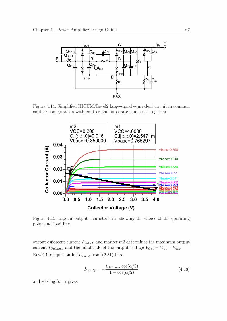
Chapter 4. Power Amplifier Design Guide 67
QBCx2
QBCx1
QdS
rBx
CrBi QjCi QdC
Csursu
QEoxQjEp QjEi QdE
rCx
rE
B
E&S
C
*
birB
*
E’
C’
iBEt
iTB’
ijBCx
ijBEp
ijBCi
ijBEi
QjSijSC
S’
Figure 4.14: Simplified HICUM/Level2 large-signal equivalent circuit in commonemitter configuration with emitter and substrate connected together.
0.5 1.0 1.5 2.0 2.5 3.0 3.50.0 4.0
0.01
0.02
0.03
0.00
0.04
Vbase=0.650Vbase=0.658Vbase=0.665Vbase=0.673Vbase=0.681Vbase=0.689Vbase=0.697Vbase=0.705Vbase=0.714Vbase=0.722Vbase=0.730Vbase=0.739Vbase=0.748Vbase=0.756Vbase=0.765Vbase=0.774Vbase=0.783Vbase=0.793Vbase=0.802
Vbase=0.811
Vbase=0.821
Vbase=0.830
Vbase=0.840
Vbase=0.850
Collector Voltage (V)
Co
lle
cto
r C
urr
en
t (A
)
m1
m2
m1VCC=C.i[::,::,0]=2.5471mVbase=0.765297
4.0000m2VCC=C.i[::,::,0]=0.016Vbase=0.850000
0.200
Figure 4.15: Bipolar output characteristics showing the choice of the operatingpoint and load line.
output quiescent current IOut Q; and marker m2 determines the maximum outputcurrent IOut max and the amplitude of the output voltage VOut = Vm1 − Vm2.
Rewriting equation for IOut Q from (2.31) here
IOut Q = −IOut max cos(α/2)
1− cos(α/2)(4.18)
and solving for α gives:

Chapter 4. Power Amplifier Design Guide 68
α = 2 arccos
(IOut Q
IOut Q − IOut max
)(4.19)
For convenience, let’s rewrite (2.35) and (2.36) here again
Idc(α) =
IOut max
2π2 sin(α/2)−α cos(α/2)
1−cos(α/2)IOut max − 2IQ ≥ 0
IQ IOut max − 2IQ < 0(4.20)
IOut = I1(α) =
IOut max
2πα−sin(α)
1−cos(α/2)IOut max − 2IOut Q ≥ 0
IOut max − IOut Q IOut max − 2IOut Q < 0(4.21)
The small-signal equivalent circuit of the power amplifier is shown in Fig. 4.16.
CBCx2
CBCx1
CdS
rBx
CrBi CjCi CdC
Csursu
CEoxCjEp CjEi CdE
rCx
rE
*
birB*
E’
C’
B’
CjS
S’
gjBCx
gjBEp
gBEt gjBEi
gjBCi gjSC
Lin
Rs
sv
Lout Rl
B
C
E&S
g0
' 'm b eg v
Figure 4.16: Small-signal equivalent circuit of the bipolar power amplifier.
Let’s combine the components of the equivalent circuit shown in Fig 4.16 in thefollowing way:
Z1 =1
gjBEi + jω(CjEi + CdE)(4.22)
Z2 =1
1/rbi + jωCrBi
(4.23)
Z3 =1
gjBEt + gjBEp + jωCjEp
(4.24)
Z4 =1
jωCEox
(4.25)
Z5 = rBx (4.26)

Chapter 4. Power Amplifier Design Guide 69
Zmu1 =1
gjBCi + jω(CjC + CdC)(4.27)
Zmu2 =1
gjBCx + jω(CBcx2 + CdS)(4.28)
Zmu3 =1
jωCBcx1
(4.29)
Zo2 =1
1/rsu + jωCsu
+1
gjSC + jωCjS
(4.30)
Additionally, the output inductance Lout at the node C is changed by the out-put inductance Lout2 at the node C’, the load resistance Rl is changed by Rl2
and output conductance g0 is placed between C’ and ground instead of E’ (seeFig. 4.17).
Z5 Z2 rCx
rE
B*
E’
C’B’
Z3
Z1
Lin
Rs
sv Lout2 Rl2
B C
E&S
Z4g0
Zmu3
Zmu2
Zmu1
Zo2
ZB’ZB*ZB
' 'm b eg v
'cv
'bv
*b
vb
v
Figure 4.17: Small-signal equivalent circuit of the bipolar power amplifier, seriesand parallel connected elements are combined into the Z components.
The load resistance Rl2 defined by the load line (see Fig. 4.15), neglecting influenceof the feedback components Zmu1, Zmu2 and Zmu3, equals
Rl2 =
VOut
IOut−VOut[go+<(1/Zo2)]− rCx
(rCx|| 1
go||<(Zo2) < VOut
IOut< 1
go+<(1/Zo2)
)&& (IOut max − IQ ≥ 0)
do not consider else(4.31)
The Miller’s theorem is applied to split the feedback components and emitterresistance (see Fig. 4.17) onto the input and output components (see Fig. 4.18).All steps required to perform this transformation are listed below:
ssg1 =vc′
vb′= −
gm1
(1/rCx+Rl2)+<(1/Zo2)+go
1 + rE(1/Z1 + gm)(4.32)

Chapter 4. Power Amplifier Design Guide 70
Zmu1pi =Zmu1
1− ssg1(4.33)
Zmu1o =Zmu1
1− 1/ssg1(4.34)
Ze1 = re(1 + Z1gm) (4.35)
Ze3 = re
(1 +
Z3gm
Z2/Z1 + Z2(Ze1 + Z1)/ (Zmu1piZ1) + 1
)(4.36)
ZB′ =Zmu1pi(Z1 + Ze1)
Z1 + Ze1 + Zmu1pi
(4.37)
ssg2 =vc′
vb∗= ssg1
ZB′
Z2 + ZB′(4.38)
Zmu2pi =Zmu2
1− ssg2(4.39)
Zmu2o =Zmu2
1− 1/ssg2(4.40)
ZB∗ =1
1/ (ZB′ + Z2) + 1/ (Z3 + Ze3) + 1/Z4 + 1/Zmu2pi
(4.41)
ssg3 =vc′
vb
= ssg2ZB∗
Z5 + ZB∗(4.42)
Zmu3pi =Zmu3
1− ssg3(4.43)
Zmu3o =Zmu3
1− 1/ssg3(4.44)
where ssg1, ssg2 and ssg2 are small-signal gains.
Now, when the input and output nodes are separated the input (ZB) and output(Zo) impedances can be calculated as:
ZB =1
1/ (ZB∗ + Z5) + 1/Zmu3pi
(4.45)
and

Chapter 4. Power Amplifier Design Guide 71
Z5 Z2B*
E’
C’B’
Z3 Z1
Lin
Rs
sv
B
E&S
Z4g0
Zmu3pi
Zmu2pi
Zmu1pi
Zmu3o
Zmu2o
Zmu1o
Zo2
rCx
Lout2 Rl2
C
Ze3 Ze1 Zee
ZB’ZB*ZB
' 'm b eg v
Figure 4.18: Small-signal equivalent circuit of the power amplifier, applying ofthe Miller’s theorem.
Zo =1
1/Zo2 + 1/Zmu1o + 1/Zmu2o + 1/Zmu3o + go
(4.46)
Then, the output inductance (Lout2) equals:
Lout2 =1
ω=(1/Zo)(4.47)
Conjugate matched theory is used to find the input inductance Lin and sourceresistance Rs:
Lin =1
ω=(1/ZB)(4.48)
and
Rs =1
<(1/ZB)(4.49)
The last unknown components in Fig. 4.16 are Rl and Lout which can be expressedas:
Rl =R4
cx + 2Rl2R3cx + ω2L2
out2R2l2 + R2
l2R2cx
−R3cx − 2R2
cxRl2 −R2l2Rcx + ω2L2
out2Rl2
(4.50)
and
Lout =R4
cx + 2Rl2R3cx + ω2L2
out2R2l2 + R2
l2R2cx
ω2Lout2(R2l2 + 2Rl2Rcx + R2
cx)(4.51)
The output power is defined as:

Chapter 4. Power Amplifier Design Guide 72
POut =
∣∣∣ VOut/[1/Rl+1/(jωLout)]rCx+1/[1/Rl+1/(jωLout)]
∣∣∣2
2Rl
=
∣∣∣ VOut
rCx[1/Rl+1/(jωLout)]+1
∣∣∣2
2Rl
(4.52)
where VOut is an amplitude of the output voltage (Vm1−Vm2) and Rl is expressedin (4.50).
Estimated output power for different output voltages (load lines) and bias cur-rents is shown in Fig. 4.19.
0.33
0.6
1.57.5
530 43
21
0
0
5
10
15
Output Voltage (V)Bias Current (uA)
Ou
tpu
t P
ow
er (
dB
m)
2
4
6
8
10
12
14
Figure 4.19: Expected output power based on the analysis of the bipolar outputcharacteristics as a function of the chosen operating point and load line.
The collector efficiency is given by:
η =POut
VdcIdc
(4.53)
where Vdc equals Vm1 + IdcrCx
The collector efficiency is shown in Fig. 4.20.
In the same way as for the CMOS design guide, the small-signal transducer powergain with compression coefficient gc is used to estimate the power added efficiency:
pae = η
(1− 1
gt
)(4.54)
where

Chapter 4. Power Amplifier Design Guide 73
0.33
0.61.5
7.5530
43
21
0
0
20
40
60
80
Bias Current (uA)Output Voltage (V)
Co
llect
or
Eff
icie
ncy
(%
)
10
20
30
40
50
60
70
Figure 4.20: Expected collector efficiency based on the analysis of the bipolaroutput characteristics as a function of the chosen operating point and load line.
gt = gcpout
pin
= gcRs
Rl
∣∣∣∣ssg3
rCx [1/Rl + 1/ (jωLout)] + 1
∣∣∣∣ (4.55)
0.33
0.61.5
7.5530
43
21
0
0
20
40
60
80
Bias Current (uA)Output Voltage (V)
Po
wer
Ad
ded
Eff
icie
ncy
(%
)
10
20
30
40
50
60
70
Figure 4.21: Estimated power added efficiency based on the analysis of the bipolaroutput characteristics as a function of the chosen operating point and load line.
Fig. 4.21 shows predicted values of the power added efficiency for the set of the

Chapter 4. Power Amplifier Design Guide 74
bias and output voltages.
As an example, the bias voltage of 0.765 V (bias current of 28.4 µA) and theoutput voltage of 3.8 V corresponds to the power added efficiency of 67.5 % withthe output power of 11.9 dBm and collector efficiency of 67.6 %. Similar to theCMOS design guide the output power can be adjusted as follow
A = A ·Round
(POut spec
POut
)(4.56)
The estimated components values for the example given above (source resistanceof 118 Ω, input inductance of 1.7 nH, output inductance of 73.1 nH and loadresistance of 456 Ω) are substituted in the harmonic balance test bench (seeFig. 4.22) to simulate the large-signal behaviour of the power amplifier prototype.
Power Sweep parameters (dBm)Frequency (Hz);Temperature (Celsius);Number of Transistors - A;Supply voltage (V); Base voltage (V);Rin (Ohm);Rout (Ohm);Lin (nH);Lout (nH).
Set
C Vout
Supply
In B
DUT
V_DC
VB
Vdc=VBase
Options
Options1
Temp=Temperature
OPTIONS
HarmonicBalance
HB1
Order[1]=9
Freq[1]=RFreq
HARMONIC BALANCEVAR
G1
Lout=73.1
Lin=1.678
Rout=456.082
Rin=118.076
Temperature=25
VCC=4.014
VBase=0.7653
A=1
RFreq=2e9
Pin_step=1
Pin_stop=-10
Pin_start=-50
Pin=-30
EqnVar
I_Probe
C
I_Probe
IoutL
L2
R=
L=Lout nH
Term
Term2
Z=Zout Ohm
Num=2
V_DC
Supply
Vdc=VCC V
P_1Tone
PORT1
Freq=RFreq
P=polar(dbmtow(Pin),0)
Z=Zin Ohm
Num=1 npn
T1
L
L1
R=
L=Lin nH
I_Probe
B
I_Probe
In
Figure 4.22: Harmonic balance test bench to design the bipolar power amplifier.
The large-signal analysis of the bipolar power amplifier prototype shows that thesaturated output power of 12 dBm (m1), collector efficiency of 65 % (m2) andpower added efficiency of 64.7 %) (m3) (see Fig. 4.23) are in a good agreementwith the predicted one (output power of 11.9 dBm, collector efficiency of 67.6 %and power added efficiency of 67.5 %).
The time domain waveforms of the collector voltage and transfer current (currentfrom the current source in the model) for different values of the input power are

Chapter 4. Power Amplifier Design Guide 75
-45 -40 -35 -30 -25 -20 -15-50 -10
-20
-10
0
10
-30
20
20
40
60
0
80
20
40
60
0
80
Input Power (dBm)
Ou
tpu
t P
ow
er
(dB
m) m1
Co
llecto
r Effic
ien
cy (%
)
m2
Po
wer A
dd
ed
Effic
ien
cy (%
)
m3
m1
Pin=
PoutdBm=12.080
-10.000
m2
Pin=
E=65.117 / 180.000
-10.000
m3
Pin=
PAE=64.714 / 180.000
-10.000
Pout
PAE
E
Figure 4.23: Output power, efficiency and power added efficiency as a function ofthe input power.
0.2 0.4 0.6 0.80.0 1.0
2
4
6
0
8
0.005
0.010
0.015
0.020
0.000
0.025
Time (nsec)
Co
llecto
r V
olt
ag
e (
V)
Co
llecto
r VC
CS
Cu
rren
t (A)
CurrentVoltage
Figure 4.24: Collector voltage and transfer current waveforms of the designedbipolar power amplifier prototype.
shown in Fig. 4.24. Higher values of the input power cause bifurcated pulses ofthe transfer current waveform.
Fig. 4.25 shows the dynamic load lines for different values of input power which

Chapter 4. Power Amplifier Design Guide 76
are located lengthways the chosen load line at the output characteristics (seeFig. 4.15).
1 2 3 4 5 6 70 8
0.01
0.02
0.03
0.00
0.04
Vbase=0.650Vbase=0.658Vbase=0.665Vbase=0.673Vbase=0.681Vbase=0.689Vbase=0.697Vbase=0.705Vbase=0.714Vbase=0.722Vbase=0.730Vbase=0.739Vbase=0.748Vbase=0.756Vbase=0.765Vbase=0.774Vbase=0.783Vbase=0.793
Vbase=0.802
Vbase=0.811
Vbase=0.821
Vbase=0.830
Vbase=0.840
Vbase=0.850
Collector Voltage (V)
Collector(Transfer)Current(A)
Figure 4.25: Large-signal simulation of the bipolar power amplifier prototype,showing dependence of the dynamic load line on the input power.

Chapter 4. Power Amplifier Design Guide 77
4.2 Load-Pull Analysis
The load-pull is a well known technique over the last three decades. It’s alsofound itself in the power amplifier design. The outcomes of this techniques area graphical representation of the interested parameters versus source or loadimpedances. For the power amplifier design such parameters are the output power,drain(collector) efficiency, power added efficiency, gain and input impedance andthe variables are the device size, supply voltage, operating point, input power,and load impedance. The load impedance is usually meant by the impedanceat fundamental harmonic but also could be expanded for the higher harmonics.The typical load-pull setup consists of a device under test, source, load and twoimpedance tuners (see Fig. 4.26).
RL 50RS 50
DUTTuner TunerSource
ZSource ZLoad
Figure 4.26: Load-pull setup.
050
100150
200
0
100
200−20
−10
0
10
20
1/GLoad
(Ω)1/BLoad
(Ω)
POut_max
=15.5 dBm @ ZLoad
=1/(1/26+1/(j*24)) Ω;
Out
put P
ower
(dB
m)
−15
−10
−5
0
5
10
15
Figure 4.27: Output power of the designed CMOS prototype power amplifier asa function of load impedance at the fundamental harmonic.
It’s clear that the pure load-pull techniques is a time consuming procedure whichhas multidimensional matrixes of the solutions at the output. Consequently, ap-

Chapter 4. Power Amplifier Design Guide 78
plying this technique at the prototype which is build previously when the tran-sistor size, supply voltage, operating point, input power and load impedance arepredefined leads to a significant reduce of the computation time.
The results of the load-pull simulation of the CMOS power amplifier proto-type with the input power of 0 dBm are shown in Fig. 4.27 (Output power),Fig. 4.28 (Drain efficiency) and Fig. 4.29 (Power added efficiency), where ZLoad =1/(GLoad + jBLoad). Fig. 4.27 shows that the power amplifier is able to achievethe output power of 15.45 dBm at the output impedance of 11.96+j12.96 Ω. Thehighest drain efficiency of 72.3 % occurs at the output impedance of 64.5+j57.1 Ωand the output impedance of 56.6 + j40.1 Ω gives the peak value of the poweradded efficiency of 67.5 %.
050
100150
200
0
100
2000
20
40
60
80
1/GLoad
(Ω)1/BLoad
(Ω)
Emax
=72.3 % @ ZLoad
=1/(1/115+1/(j*130)) Ω;
Dra
in E
ffic
ien
cy (
%)
10
20
30
40
50
60
70
Figure 4.28: Drain efficiency of the designed CMOS prototype power amplifier asa function of load impedance at the fundamental harmonic.
Table 4.1 makes the comparison of the CMOS power amplifier prototype per-formance at each step of the design procedure (analytical analysis, large-signalsimulation at the saturation and load-pull analysis).

Chapter 4. Power Amplifier Design Guide 79
050
100150
200
0
100
2000
20
40
60
80
1/GLoad
(Ω)1/BLoad
(Ω)
PAEmax
=67.5 % @ ZLoad
=1/(1/85+1/(j*120)) Ω;P
ow
er A
dd
ed E
ffic
ien
cy (
%)
10
20
30
40
50
60
70
Figure 4.29: Power added efficiency of the designed CMOS prototype power am-plifier as a function of load impedance at the fundamental harmonic.
Table 4.1: Summary table, showing the analytically estimated and simulated per-formances of the CMOS prototype power amplifier.
Analytical Large-signal Load-pullAnalysis Simulation Analysis
Transistor Type NANA NANA NANAGate Fingers Connection one side one side one sideLength 0.4 0.4 0.4 µmWidth 1000 1000 1000 µmNumber of Fingers 40 40 40Supply Voltage 1.65 1.65 1.65 VBias Voltage 0.4 0.4 0.4 VInput Power N/A 0 -0.67 dBmOutput Impedance 54.7 + j43.2 54.7 + j43.2 56.6 + j40.1 ΩSource Impedance 5.2 + j34.5 5.2 + j34.5 6.2 + j30 ΩOutput Power 11.59 11.56 11.5 dBmDrain Efficiency 70.7 71.79 71.9 %Power Added Efficiency 65.7 66.78 67.5 %

Chapter 4. Power Amplifier Design Guide 80
4.3 Transformer-Based Matching Network De-
sign
There exists a lot of matching network configurations all of them has some ad-vantages and drawbacks which has to be considered to make the right choice. Theanalytical analysis of the matching network help to make a fast estimation of therequired components and to predict its loss. This part gives a derivation of theequation set for the transformer-based matching network.
The matching network could include ”parasitic” components such as bond wires,bond pads and parasitic capacitors.
4.3.1 Analysis of Bond Wires
The aim of the analysis presented here is to give the analytical equations for theseries inductance and series resistance of the bond wire connection (see Fig. 4.30).
1 2Ls1(Ls2) Rs1(Rs2)
Figure 4.30: Typical RF lumped model of the bond wire connection.
Fig. 4.31 shows the solid model used for analytical analysis. It consists of thebond wires and their images in accordance with the theory of ”current images”which are approximated by the three strait filaments. The one bond wire and twobond wires systems are considered.
The component values of inductance (Ls1) and resistance (Rs1) [March 91] forthe single bond wire are given by:
Ls1 = L1 + L2 + L3 − 2M12 − 2M23 − 2M13
− M11im −M12im −M13im
− M21im −M23im −M22im
− M31im −M32im −M33im (4.57)
and
Rs1 =
Rdc cosh[0.041( d
ds)2
]dds≤ 3.394
Rdc
(0.25 d
ds+ 0.2654
)dds≥ 3.394
(4.58)
where L is a self inductance of the strait filaments; M is a mutual inductancesbetween strait filaments; Rdc = 4ρl/(πd2) is a dc resistance of the bond wire; d is

Chapter 4. Power Amplifier Design Guide 81
l1(l4)(x1,y1,z1)
l2(l5) l3(l6)
(x2,y2,z2) (x3,y3,z3)
(x4,y4,z4)
l1im(l4im)
(x1,y1,-z1)
l2im(l5im)l3im(l6im)
(x2,y2,-z2) (x3,y3,-z3)
(x4,y4,-z4)
Ground Plane
Bond wires images
used to model back currents
Bond wires
X
Z
Chip
(a)
(x1,y1,z1)
(x2,y2,z2) (x3,y3,z3)
(x4,y4,z4)
(x1,y1+s,z1)
(x2,y2+s,z2) (x3,y3+s,z3)
(x4,y4+s,z4)
l1(l1im) l2(l2im) l3(l3im)
l4(l4im) l5(l5im) l6(l6im)X
Y
(b)
Figure 4.31: Solid model used for the analytical analysis of the bond wire con-nection.: (a) Front view; (b) Top view.
a diameter of the bond wire; and ds is a skin depth of the bond wire material atgiven frequency:
ds =
√ρ
πfµ0µr
(4.59)
where ρ is resistivity of the bond wire material (2.62 · 10−8 Ω ·m for aluminium);and f is frequency (Hz).
In case of two parallel bond wires the inductance (Ls2) and resistance (Rs2) aregiven by:

Chapter 4. Power Amplifier Design Guide 82
Ls2 =Ls1
2+
M14 −M14im + M15 −M15im + M16 −M16im
2
+M24 −M24im + M25 −M25im + M26 −M26im
2
+M34 −M34im + M35 −M35im + M36 −M36im
2(4.60)
and
Rs2 =FpRs1
2(4.61)
where Fp is the proximity factor [March 91]:
Fp = 1 + 0.8478 exp[−0.9435(s/d)] (4.62)
The self inductances in (4.57) and (4.61) can be expressed by the inductance of astrait wire positioned horizontally at infinite distance above ground [March 91]:
L =µ0l
2π
ln
4l
d+
√1 +
(2l
d
)2 +
d
2l−
√1 +
(d
2l
)2
+ µrδ
(4.63)
where µ0 is permeability of free space (4π · 10−7H/m); µr is relative permeabilityof the bond wire material; l is a length of the bond wire; d is a diameter of thebond wire; δ is a skin effect factor.
The skin effect factor was introduced to take care about a high frequency effectand equals:
δ = 0.25 tanh(4ds/d) (4.64)
where ds is a skin depth of the bond wire material at given frequency.
l
m
R
Figure 4.32: Unequal filaments meeting at a point.

Chapter 4. Power Amplifier Design Guide 83
The mutual inductances M12 between l1 and l2; M23 between l2 and l3 in (4.60)and (4.57) are expressed by the mutual inductance between two unequal filamentsmeeting at a point (see Fig. 4.32) [Grover 46]:
M =µ0
2πcos ϕ
(l tanh−1 m
l + R+ m tanh−1 l
m + R
)(4.65)
cos ϕ =l2 + m2 −R2
2lm(4.66)
where l and m are the length of the filaments; ϕ is the angle between filaments;and R is the distance between their ends.
l
m
R1
R2
R4
R3
Figure 4.33: Unequal filaments in the sam plane, not meeting.
The mutual inductances M13 between l1 and l3; M11im between l1 and l11im;M12im between l1 and l12im; M13im between l1 and l13im; M21im between l2 andl11im; M22im between l2 and l12im; M23im between l2 and l13im; M31im between l3and l11im; M32im between l3 and l12im; M33im between l3 and l13im are representedby the mutual inductances between two unequal filaments in the same plane, notmeeting (see Fig. 4.33) [Grover 46]:
M =µ0
2πcos ϕ
[(µ + l) tanh−1 m
R1 + R2
+ (ν + m) tanh−1 l
R1 + R4
− µ tanh−1 m
R3 + R4
− ν tanh−1 l
R2 + R3
](4.67)
cos ϕ =α2
2lm(4.68)
where α2 = R24 − R2
3 + R22 − R2
1; l and m are the length of the filaments; R1,R2, R3, and R4 are the distances between the ends of the filaments as shown inFig. 4.33; and lengths µ and ν are given by:
µ =[2m2 (R2
2 −R23 − l2) + α2 (R2
4 −R23 −m2)] l
4l2m2 − a4(4.69)

Chapter 4. Power Amplifier Design Guide 84
ν =[2l2 (R2
4 −R23 −m2) + α2 (R2
2 −R23 − l2)] m
4l2m2 − a4(4.70)
m
l
R1
R2
R3
R4
d
Figure 4.34: Mutual inductance of two straight filaments placed in any desiredpositions.
The mutual inductances M14im between l1 and l4im; M15 between l1 and l5; M15im
between l1 and l5im; M16 between l1 and l6; M16im between is l1 and l6im; M24
between l2 and l4; M24im between l2 and l4im; M25im between l2 and l5im; M26
between l2 and l6; M26im between l2 and l6im; M34 between l3 and l4; M34im
between l3 and l4im; M35 between l3 and l5; M35im is between l3 and l5im; M36im
between l3 and l6im are represented by the mutual inductance of two straightfilaments placed in any desired positions (see Fig. 4.34) [Grover 46]:
M =µ0
2πcos ϕ
[(µ + l) tanh−1 m
R1 + R2
+ (ν + m) tanh−1 l
R1 + R4
− µ tanh−1 m
R3 + R4
− ν tanh−1 l
R2 + R3
]− Ωd
sin ϕ(4.71)
Ω = tan−1
[d2 cos ϕ + (µ + l)(ν + m) sin2 ϕ
dR1 sin ϕ
]
− tan−1
[d2 cos ϕ + (µ + l)ν sin2 ϕ
dR2 sin ϕ
]
+ tan−1
[d2 cos ϕ + µν sin2 ϕ
dR3 sin ϕ
]
− tan−1
[d2 cos ϕ + µ(ν + m) sin2 ϕ
dR4 sin ϕ
](4.72)
cos ϕ =α2
2lm(4.73)

Chapter 4. Power Amplifier Design Guide 85
where α2 = R24 − R2
3 + R22 − R2
1; d2 = R23 − µ2 − ν2 + 2µν cos ϕ; ϕ is the angle
between the filament l and intersection line which is produced by the planes whichare passed through through the filaments l and m in such a way as to intersectat right angles; and lengths µ and ν are given by:
µ =[2m2 (R2
2 −R23 − l2) + α2 (R2
4 −R23 −m2)] l
4l2m2 − a4(4.74)
ν =[2l2 (R2
4 −R23 −m2) + α2 (R2
2 −R23 − l2)] m
4l2m2 − a4(4.75)
The mutual inductances M14 between l1 and l4; M25 between l2 and l5; M36
between l3 and l6 are represented by the mutual inductance of two equal parallelstraight filaments [Grover 46]:
M =µ0
2πl
[log
l
s+
√1 +
l2
s2−
√1 +
s2
l2+
s
l
](4.76)
where l is the length of filaments; and s is the distance between them.
Table 4.2 contains the bond wire coordinates which approximate typical bondwires used during this work for connecting of the input (one bond wire) andoutput (two bond wires with 50 µm pitch) pads.
Table 4.2: Bond wires coordinates for analytical analysis.Points Bond Wire 1 Bond Wire 2
X Y Z X Y Z1 0 0 700 0 50 700 µm2 84 0 800 84 50 800 µm3 250 0 800 250 50 800 µm4 500 0 500 500 50 500 µm
Components of the equivalent circuit (series resistance and inductance) for bondwires which shape is described in Table 4.2 are calculated and shown in Fig. 4.35.

Chapter 4. Power Amplifier Design Guide 86
0 5 10 15 20 25 300.0
0.1
0.2
0.3
0.4
0.5
0.25
0.30
0.35
0.40
0.45
0.50
One Bond wire Two Bond wires
Ser
ies
Res
ista
nce
()
Frequency (GHz)
Ser
ies
Indu
ctan
ce (n
H)
Figure 4.35: Frequency behaviour of analytically estimated series resistance andseries inductance of typical bond wire configurations: one bond wire and twoparallel bond wires with a pitch of 50 µm.

Chapter 4. Power Amplifier Design Guide 87
4.3.2 Analysis of Transformer as Matching Network
Transformers are produced in different technologies and have different configu-rations (metal stack, winding scheme etc.) but all of them can be described byinductance of the windings, quality factor of the windings and coupling coeffi-cients between them.
Lp Ls
K
Rp Rs
P+ S-
(a)
Xs-Xm
Rs=Xs/Qs
Xp-Xm
Rp=Xp/Qp
Bm=-1/Xm
m s pX =K X X
P+ S-
p pX = L
s sX = L
(b)
Figure 4.36: Transformer: (a) Lumped model; (b) Equivalent T-model.
The simplified transformer model is shown in Fig. 4.36(a). The equivalent T-model (see Fig. 4.36(b)) is used here to perform analytical analysis of the trans-former based matching network.
Xs-Xm
Rs=Xs/Qs
Xp-Xm
Rp=Xp/Qp
Bm=-1/XmBIn BLGIn GL
Transformer
m s pX =K X X
ZL
Z22
Z2Z3
ZInZ12
Z1
Z32
outv
inv
mv
Figure 4.37: Transformer-based matching network.
Fig. 4.37 shows typical example of the transformer-based matching network. Thematching network has to transform load admittance GL into input admittanceGIn. This circuit has seven unknowns such as load capacitive susceptance BL, in-put capacitive susceptance BIn, inductive reactance of the primary winding Xp,inductive reactance of the secondary winding Xs, quality factor of the primarywinding Qp, quality factor of the secondary winding Qs and coupling coefficientbetween them K that leads to unbounded solution sets. To overcome this un-certainty, the quality factors and coupling coefficient are treated as technology

Chapter 4. Power Amplifier Design Guide 88
and winding scheme limiting factors that leads to the reduction of the number ofunknowns and unambiguous solution.
The conjugate matching theory is applied to formulate four equations to solvethe system with four unknowns:
G3 = GIn
B3 = −BIn
G32 = GL
B32 = −BL
(4.77)
Load impedance ZL equals to RL + jXL where
RL =GL
G2L + B2
L
(4.78)
and
XL = − BL
G2L + B2
L
(4.79)
Internal impedance Z1 equals to R1 + jX1. Its components are expressed as
R1 = RL + Rs (4.80)
and
X1 = XL + Xs −Xm (4.81)
Transforming the impedance components R1 and X1 into the admittance compo-nents G1 and B1 gives:
G1 =R1
R21 + X2
1
(4.82)
and
B1 = − X1
R21 + X2
1
(4.83)
Admittance Y2 = G2 + jB2 where G2 and B2 equal:
G2 = G1 (4.84)
and

Chapter 4. Power Amplifier Design Guide 89
B2 = B1 + Bm (4.85)
Then transformation of Y2 into Z2 gives:
R2 =G2
G22 + B2
2
(4.86)
and
X2 = − B2
G22 + B2
2
(4.87)
Components R3 and X3 of the internal impedance Z3 are:
R3 = R2 + Rp (4.88)
and
X3 = X2 + Xp −Xm (4.89)
Finally G3 and B3 are expressed as:
G3 =R3
R23 + X2
3
(4.90)
and
B3 = − X3
R23 + X2
3
(4.91)
Performing the same operation from the left to the right the last two terms (G32
and B32) in (4.77) can be found:
RIn =GIn
G2In + B2
In
(4.92)
XIn = − BIn
G2In + B2
In
(4.93)
R12 = RIn + Rp (4.94)
X12 = XIn + Xp −Xm (4.95)

Chapter 4. Power Amplifier Design Guide 90
G12 =R12
R212 + X2
12
(4.96)
B12 = − X12
R212 + X2
12
(4.97)
G22 = G12 (4.98)
B22 = B12 + Bm (4.99)
R22 =G22
G222 + B2
22
(4.100)
X22 = − B22
G222 + B2
22
(4.101)
R32 = R22 + Rs (4.102)
X32 = X22 + Xs −Xm (4.103)
G32 =R32
R232 + X2
32
(4.104)
B32 = − X32
R232 + X2
32
(4.105)
Substituting (4.90), (4.91), (4.104) and (4.105) in to (4.77) and solving it for Xs,BL, Xp and BIn gives:
Xs =Qs
√K2QpQs+1
GL(1+K2QpQs+Q2s)
BL = QsGL√K2QpQs+1
Xp =Qp
√K2QpQs+1
GIn(1+K2QpQs+Q2p)
BIn = QpGIn√K2QpQs+1
(4.106)
Next step is to calculate the efficiency of the transformer matching network.Assumption that the matching network is driven by the current source on the leftside in such way that vin = 1 gives:

Chapter 4. Power Amplifier Design Guide 91
vm =Z2
Z3
(4.107)
Then, the output voltage equals:
vout =vmZL
Z1
(4.108)
Finally, the power delivered to the load is:
Pout =|vout|2GL
2(4.109)
and power available from the source is:
Pavs =GIn
2(4.110)
Then, the efficiency of the matching network when the input and output aresimultaneously matched equals:
E =Pout
Pavs
· 100
∣∣∣∣Xs=
Qs
√K2QpQs+1
GL(1+K2QpQs+Q2s)
,BL=QsGL√
K2QpQs+1
=QpQsK
2√
QpQsK2 + 1
2QpQsK2 + QpQsK2√
QpQsK2 + 1 + 2√
QpQsK2 + 1 + 2· 100
=1
1 + 2QpQsK2 + 2
√1
QpQsK2
(1 + 1
QpQsK2
) · 100 (4.111)
The same answer for E, using another approach, is derived in [Aoki 02,a].
Fig. 4.38 shows the efficiency of the transformer-based matching network for caseswhen the coupling coefficient equals 1 (see Fig. 4.38(a)), 0.8 (see Fig. 4.38(b)), 0.6(see Fig. 4.38(c)), 0.4 (see Fig. 4.38(d)). Typical integrated transformers have thecoupling coefficient in the range from 0.6 to 0.8 and the winding quality factorin the range from 5 to 15 so the expected efficiency of the transformer-basedmatching network is between 50 % (-3 dB) and 80 % (-1 dB).
The next step is to design the transformer with predicted parameters of Qp,Qs, K, Lp and Ls. The designed transformer requires a method to estimated itsperformance. The way how to do it is described below.
The definition of maximum transducer power gain [Gonzalez 97], under simulta-neous conjugate match condition gives the minimum power loss of the transformerand is given by:

Chapter 4. Power Amplifier Design Guide 92
05
1015
2025
05
1015
2025
0
20
40
60
80
100 E=67.21%@Qs=Qp=5
E=87.53%@Qs=Qp=15
Qp
E=92.31%@Qs=Qp=25
E=90.49%@Qs=Qp=20
Qs
E=81.9%@Qs=Qp=10
Eff
icie
ncy
(%
)
10
20
30
40
50
60
70
80
90
(a)
05
1015
2025
05
1015
2025
0
20
40
60
80
100 E=60.96%@Qs=Qp=5
E=84.66%@Qs=Qp=15
Qp
E=90.49%@Qs=Qp=25
E=88.27%@Qs=Qp=20
E=77.93%@Qs=Qp=10
Qs
Eff
icie
ncy
(%
)
10
20
30
40
50
60
70
80
90
(b)
05
1015
2025
05
1015
2025
0
20
40
60
80
100 E=51.95%@Qs=Qp=5
E=80.11%@Qs=Qp=15
Qp
E=87.53%@Qs=Qp=25 E=84.66%@Qs=Qp=20
E=71.76%@Qs=Qp=10
Qs
Eff
icie
ncy
(%
)
10
20
30
40
50
60
70
80
90
(c)
05
1015
2025
05
1015
2025
0
20
40
60
80
100
E=38.2%@Qs=Qp=5
E=71.76%@Qs=Qp=15
Qp
E=81.9%@Qs=Qp=25
E=77.94%@Qs=Qp=20
Qs
E=60.96%@Qs=Qp=10E
ffic
ien
cy (
%)
10
20
30
40
50
60
70
80
90
(d)
Figure 4.38: Efficiency of the transformer-based matching network: (a) K=1;(b) K=0.8; (c) K=0.6; (d) K=0.4.
Gp,max = 10 log
[ |S21||S12|
(K −
√K2 − 1
)](4.112)
where
K =1− |S11|2 − |S22|2 + |∆|2
2|S12S21| (4.113)
and
∆ = S11S22 − S12S21 (4.114)
The loss of the transformer in the case of zero source admittance (idealised outputof the transistor) can be expressed as:
Loss = −10 log|S21|2
1− |S11|2 (4.115)

Chapter 4. Power Amplifier Design Guide 93
The value in (4.115) equals to (4.112) when the output is loaded by the impedancefor simultaneous conjugate match.
The values of the input(ΓMs) and output(ΓMl) reflection coefficients required forsimultaneous conjugate match are:
ΓMs =B1 ±
√B2
1 − 4|C1|22C1
(4.116)
and
ΓMl =B2 ±
√B2
2 − 4|C2|22C2
(4.117)
where
B1 = 1 + |S11|2 − |S22|2 − |∆|2 (4.118)
B2 = 1 + |S22|2 − |S11|2 − |∆|2 (4.119)
C1 = S11 −∆S∗22 (4.120)
C2 = S22 −∆S∗11 (4.121)
The minus sign must be used in (4.116) and (4.117) when calculating the simulta-neous conjugate match for an unconditionally stable two-port network [Gonzalez 97].
Finally the required impedances or admittances for the simultaneously matchcondition can be extracted from (4.116) and (4.117) as:
ZMs = Z01 + ΓMs
1− ΓMs
(4.122)
and
ZMl = Z01 + ΓMl
1− ΓMl
(4.123)
or
YMs =1
ZMs
(4.124)
and
YMl =1
ZMl
(4.125)

Chapter 4. Power Amplifier Design Guide 94
4.4 Final Design
The circuit diagram of the final design is shown in Fig. 4.39. It is a one stagepush-pull CMOS power amplifier. It consists of two single transistors which areworking in a differential mode that creates a virtual ground for the odd harmonicsbetween the sources and relax requirements for the ground connection.
3.2
nH
3.2
nH
0.9
nH
0.9
nH
VSupply
RL
50
1.1
1.1
3.8
3.8
RBond
75 m
LBond
0.35 nH5.3
pF
CPad
200 fF
5.3
pF
0.9
pF
0.9
pF
2.1
nH
2.1
nH
0.6
nH
0.6
nH
VBias
RS
50
0.7
0.7
2.5
2.5
RBond
130 m
LBond
0.44 nH7.1
pF
CPad
100 fF
7.1
pF
K
0.6
0.6
K
K
0.6
0.6
K
M1
1mm/
0.4um/
40
M2
1mm/
0.4um/
40
vS
Rg1
5.21
Rg2
5.21
Figure 4.39: Circuit diagram of the one stage push-pull CMOS power amplifier.
The 50 Ω load resistance presents the prevalent characteristic impedance in theRF design. Then the output pad is bonded by two bond wires which series in-ductance of 0.35 nH and resistance of 75 mΩ are calculated in the previous part(see Fig. 4.35). The pad is modelled by the capacitor with a capacitance of 200 fFto the ground. The output transformer with capacitors perform the transforma-tion of the single-ended impedance to the differential of 2(56.6 + j40.1) Ω (seedrain load diff. in Fig. 4.40) that is estimated during the load-pull simulation (seeTable 4.1). The input matching network (the input transformer and capacitors)transfers differential input impedance of the transistors of 2(6.2 + j30) Ω (seeTable 4.1) into the single ended impedance. The input pad is two times smallerin comparison with the output one and it is modelled by the capacitor of 100 fFand bonded by the one bond wire with series inductance of 0.44 nH and seriesresistance of 130 mΩ (see Fig. 4.35). The component values of the input matchingnetwork is calculated in such way that input impedance of the power amplifierequals to 50 Ω (see input impedance in Fig. 4.40).
The transfer characteristic of the final power amplifier is shown in Fig 4.41. Thepower amplifier has the maximum power added efficiency of 39.2 % at the inputpower of 8 dBm with the output power of 14.2 dBm and drain efficiency of 51.6 %.The output power of the final power amplifier is about 1.1 dB higher as it is ex-pected from the prototype design 11.4 dBm + 3 dB - 1.444 dB (where 11.4 dBm isthe output power of the single ended prototype, 3 dB is an increase due to power

Chapter 4. Power Amplifier Design Guide 95
0.2 0.5 1.0 2.0 5.0
-0.2j
0.2j
-0.5j
0.5j
-1.0j
1.0j
-2.0j
2.0j
-5.0j
5.0j
Input Impedance
Drain Load Diff.
2.3 GHz
1.7 GHz
1.9 GHz
Figure 4.40: Frequency response of the input impedance and differential load ofthe drains of the one stage CMOS push-pull power amplifier. Z Smith chart isnormalized to 50 Ω impedance.
combining of two amplifiers, - 1.444 dB is the loss of the output matching net-work). The output power increase is due to the fact that final transformer-basedCMOS power amplifier operates similar to inverse Class-F amplifier [Wei 00] in-stead of Class-B operation of the designed CMOS prototype amplifier (compareFig. 4.42 and Fig. 4.11).
Finally large-signal frequency response at input power of 8 dBm is shown inFig. 4.43. The input power of 8 dBm is chosen in accordance with power transfercharacteristic presented in Fig. 4.41 as the power added efficiency reaches itsmaximum at this input power. The frequency response shows that the maximumsof the output power, drain efficiency and power added efficiency are very close tothe chosen operating frequency of 1.9 GHz.

Chapter 4. Power Amplifier Design Guide 96
m1
Pin=
PoutdBm=14.168
8.000
m2
Pin=
E=51.641
8.000
m3
Pin=
PAE=39.161
8.000
-40 -30 -20 -10 0-50 10
-40
-20
0
-60
20
10
20
30
40
50
0
60
10
20
30
40
50
0
60
Input Power (dBm)
Ou
tpu
t P
ow
er
(dB
m)
m1
Dra
in E
fficie
ncy (%
)
m2
Po
wer A
dd
ed
Effic
ien
cy (%
)
m3
m1
Pin=
PoutdBm=14.168
8.000
m2
Pin=
E=51.641
8.000
m3
Pin=
PAE=39.161
8.000
Pout
PAE
E
Figure 4.41: Transfer characteristics of the one stage push-pull CMOS poweramplifier at the operating frequency of 1.9 GHz, showing output power (14.2 dBm)and drain efficiency (51.6 %) at the highest power added efficiency (39.2 %).
0.200 0.400 0.600 0.8000.000 1.000
1
2
3
0
4
0.00
0.01
0.02
0.03
0.04
-0.01
0.05
Time (nsec)
Dra
in V
olt
ag
e (
V)
Ch
an
nel C
urre
nt (A
)
Current
Voltage
Figure 4.42: Drain voltage and channel current waveforms of the one shoulder,showing inverse Class-F operation of the push-pull transformer-based CMOSpower amplifier.

Chapter 4. Power Amplifier Design Guide 97
1.8G 1.9G 2.0G 2.1G 2.2G1.7G 2.3G
11
12
13
14
10
15
25
30
35
20
40
40
45
50
35
55
Frequency (Hz)
Ou
tpu
t P
ow
er
(dB
m) D
rain
Effic
ien
cy (%
)
Po
wer A
dd
ed
Effic
ien
cy (%
)
Pout
PAE
E
Figure 4.43: Frequency response of the one stage push-pull CMOS power amplifierat the input power of 8 dBm.

Chapter 5
Experimental Results
The aim of this work is the building of fully monolithically-integrated power am-plifiers. The transformer-based push-pull architecture is used as the basic circuitfor our investigation. The main advantage of the push-pull architecture is therelaxed requirements for the ground connections, but for the single ended inputand output ports additional input and output baluns are required. At first themonolithically integrated power amplifiers with an external matching network areinvestigated. Fig. 5.1 gives an example of the two-stage transformer-based CMOSpower amplifier with an external matching network [Vasylyev 04].
C 1
C 2
X1M2
M3
M1
X2
C 3
C 4
M4
M5
M6
Z1
/ 4λ
1θ
Z1
/ 4λ
1θ
RFOUT +
RFOUT -RFIN -
RFIN +
VDDC 4
VDD
C 5
VDD VBias 2VBias 1
Monolithic Integrated
Power Amplifier
PCB Matching
Network
Substrate
ZLZ IN
Figure 5.1: Circuit diagram of the power amplifier.
This power amplifier was mounted on the Rogers RO4003 microwave substrate
98

Chapter 5. Experimental Results 99
with a λ/4 matching network (see Fig. 5.2). The matching network requires anarea of 25 mm x 50 mm.
Figure 5.2: Photograph of the power amplifier board (size 50 mm x 50 mm).
As alternative solutions to the external matching network, following on chipmatching network topologies are investigated: the LC-based network, transformer-based matching network and power combining transformer.
The LC-based network (see Fig. 5.3(a)) combines the functions of matching andphase inversion required for the proper push-pull operation. The componentsform complementary low-pass (C1, L1, L3) and high-pass (C2, L2, C3) circuitson respective push-pull shoulders with the same impedance transformation ratio.Additional a dc blocking capacitor C4 is added in front.
The transformer-based matching network (see Fig. 5.3(b)) consists of the trans-former X1 with a center tap on the primary winding and capacitors C1, C2, andC3. The capacitors together with the winding inductances of the transformer forma parallel resonant tank.
If one transformer-based power amplifier is not able to deliver the required out-put power or bandwidth, the power combining transformer structure can be used[Vasylyev 05,b]. The power combining transformer shown in Fig. 5.3(c)) con-sists of four transformer-based networks. The secondary windings of transformers

Chapter 5. Experimental Results 100
X1, X2 and transformers X3, X4 are connected in series and then they are con-nected in parallel. Such connection of transformers in ideal case delivers the sameimpedance to each power amplifier as a single transformer.
L1
L2
L3
C3
C4OutK
X1 Out
C1
C2
C3
C4
C5
C6
C7
C8
Out
X1
X2
X3
X4
C9
C3C1
C2
InP
InN
C1
C2
InP
InN
InP1
InN1InN2
InP2InP3
InN3InN4
InP4
(a)
(b)
(c)
Figure 5.3: Output matching networks. Circuit diagrams: (a) LC-based matchingnetwork; (b) Transformer-based matching network; (c) Power combining trans-former.
The 2 GHz realisations of the previously discussed matching networks are shownin Fig. 5.4. The inductors L1 and L2 of the LC-based matching networks (seeFig. 5.4(a)) are combined in to the one center-tapped inductor. The capacitor C4is placed above the capacitor C3 to eliminate an additional parasitic capacitanceto the lossy substrate at the output node of the matching network. This matchingnetwork occupies the area of 460 µm x 410 µm. The transformer-based matchingnetwork (see Fig. 5.4(b)) occupies the area of 330 µm x 380 µm. The powercombined transformer structure shown in Fig. 5.4(c) has a four times larger areaand equals to 1320 µm x 380 µm.
The amplifiers made during this work cover four frequency bands (2 GHz, 5 GHz,17 GHz and 26 GHz) and use two technologies (a 0.13 µm CMOS and 28 GHz fT
SiGe-bipolar). Fig. 5.5 summarizes the performance of the power amplifiers. Also,the latest results of the fully monolithically integrated transformer-based poweramplifiers are additionally highlighted by the red circle and described below inmore detail.

Chapter 5. Experimental Results 101
(a)
(b)
(c)
X1
X1
X2
X3
X4
L1&L2
L3
C3&C4
33
0 u
m
33
0 u
m
1.3
2 m
m
165 um
Figure 5.4: Chip photos of the 2 GHz output matching networks: (a) LC-basedmatching network; (b) Transformer-based matching network; (c) Power combin-ing transformer.

Chapter 5. Experimental Results 102
(a)
(b)
Figure 5.5: Performance of the most interesting experimental results of the poweramplifiers which are made during this work: (a) Output power; (b) Power addedefficiency.

Chapter 5. Experimental Results 103
5.1 2 GHz CMOS Transformer-Based Power Am-
plifier
The circuit diagram of the fully monolithically-integrated CMOS DECT poweramplifier is shown in Fig. 5.6. The thick gate oxide NMOS transistors in thecascode configuration are used in this design to satisfy the maximum power supplyrequirement of 3.5 V. A two stage configuration is used to amplify the inputpower of 5 dBm to the output power above 26.5 dBm (in accordance with DECTspecification).
VSSDriver
VDDDriverVBiasDriver
M31.1mm/
400nm/
50
VSSOut
RFInP
RFInN
C19.3 pF
C29.3 pF
X1Lp=1.24 n
Ls=1.41 n
K=0.77
M41.1mm/
400nm/
50
M1100µm/
400nm/
5
C59.9 pF
C69.9 pF
X2Lp=0.39 n
Ls=1.1 n
K=0.7
M6100µm/
400nm/
5
VBiasOut
R150
R350 M2
2mm/
400nm/
50
M52mm/
400nm/
50
M78mm/
400nm/
180
M84.5mm/
400nm/
180
M94.5mm/
400nm/
180
M108mm/
400nm/
180
R250
VBiasCOut
R41 k
VBiasCOut
VDDPDriver
C340 pF
C760 pFC4
160 pF
VDDOut
C916.8 pF
C1016.8 pF
RFOut
VSSOut
C111.7 pF
C8260 pF
X3Lp=0.36 n
Ls=1.75 n
K=0.8
Figure 5.6: Simplified circuit diagram of the 2 GHz CMOS fully integrated poweramplifier.
The output matching network is a crucial component of the power amplifier; andthe output transformer has the highest influence on its performance. The simu-lated differential S-parameters of the output transformer are shown in Fig. 5.7.
(a) (b)
Figure 5.7: S-parameter simulation results for the output transformer: (a) S11,S22; (b) S12, S21.

Chapter 5. Experimental Results 104
The inverse of the real part of the required admittances for the simultaneouslymatch condition are shown in Fig. 5.8(a). The minimum power loss of 1.68 dB atthe frequency of 1.9 GHz under above condition can be achieved for the parallelsource resistance of 7.8 Ω and parallel load resistance of 34.4 Ω (see Fig. 5.8(b)).
(a) (b)
Figure 5.8: Output transformer simulation results: (a) Parallel source and load re-sistances required for the simultaneous conjugate match condition; (b) Minimumpower loss.
The simplified circuit diagram of the transformer-based matching network isshown in Fig. 5.9. The matching network consists of the transformer X3, tuningcapacitor C11 and parasitic elements of bond wires Lb1, R1, Lb2 and R2. Thevalue of the capacitor C11 is optimized to reduce the power loss of the matchingnetwork.
X3Lp=0.36 n
Ls=1.75 n
K=0.8+
Lb10.35 nH
C111.7 pF
Rb180 m
Lb20.17 nH
Rb140 m
-
RLoad
50
2.18+j4.26
@1.9 GHz
Figure 5.9: Transformer-based output matching network.
The input impedance and power loss of the output matching network are shown inFig. 5.10. The output matching network has 1.85 dB of power loss and transformsthe single ended 50 Ω load into the differential input impedance of 2.18+j4.26 Ωat 1.9 GHz. In the final circuit (see Fig. 5.6), the capacitors C9 and C10 as well asparasitic output capacitances of the transistors M7, M8, M9 and M10 compensatethe imaginary part that gives the final impedance of 10.5 Ω.
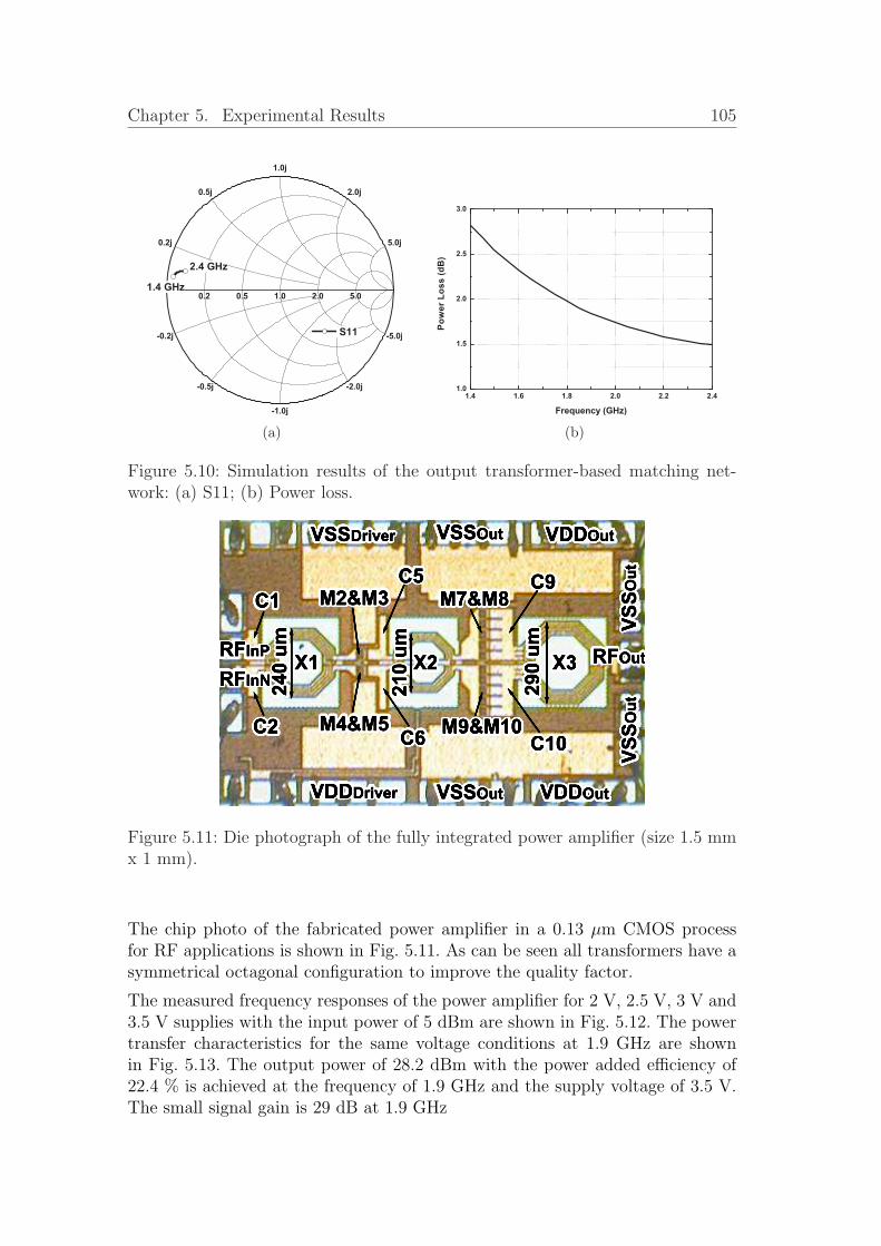
Chapter 5. Experimental Results 105
(a) (b)
Figure 5.10: Simulation results of the output transformer-based matching net-work: (a) S11; (b) Power loss.
Figure 5.11: Die photograph of the fully integrated power amplifier (size 1.5 mmx 1 mm).
The chip photo of the fabricated power amplifier in a 0.13 µm CMOS processfor RF applications is shown in Fig. 5.11. As can be seen all transformers have asymmetrical octagonal configuration to improve the quality factor.
The measured frequency responses of the power amplifier for 2 V, 2.5 V, 3 V and3.5 V supplies with the input power of 5 dBm are shown in Fig. 5.12. The powertransfer characteristics for the same voltage conditions at 1.9 GHz are shownin Fig. 5.13. The output power of 28.2 dBm with the power added efficiency of22.4 % is achieved at the frequency of 1.9 GHz and the supply voltage of 3.5 V.The small signal gain is 29 dB at 1.9 GHz

Chapter 5. Experimental Results 106
1.4 1.6 1.8 2.0 2.2 2.45
10
15
20
25
30
35
0
5
10
15
20
25
Input Power: 5 dBmSupply:
2 V 2.5 V 3 V 3.5 V
Out
put P
ower
(dB
m)
Frequency (GHz)
Pow
er A
dded
Eff
icie
ncy
(%)
Figure 5.12: Measured frequency response of the fully integrated power amplifier.
1.4 1.6 1.8 2.0 2.2 2.45
10
15
20
25
30
35
0
5
10
15
20
25
Input Power: 5 dBmSupply:
2 V 2.5 V 3 V 3.5 V
Out
put P
ower
(dB
m)
Frequency (GHz)
Pow
er A
dded
Eff
icie
ncy
(%)
Figure 5.13: Measured power transfer characteristics of the fully integrated poweramplifier.

Chapter 5. Experimental Results 107
5.2 5 GHz CMOS Transformer-Based Power Am-
plifier
The circuit diagram of the CMOS fully monolithically-integrated power amplifierfor the WLAN 802.11a is shown in Fig. 5.14. The power amplifier is implementedin a 0.13 µm RF CMOS technology.
VSSDriver
VDDDriverVBiasDriver
M2360 um/
0.12 um
40VSSOut
RFInP
RFInN
RFOutC12 pF
C22 pF
X1Lp=0.81 n
Ls=0.31 n
K=0.65
M3360 um/
0.12 um
40
M136 um/
0.12 um
4
C31.6 pF
C41.62 pF
X2Lp=0.31 n
Ls=0.8 n
K=0.65
M4100 um/
0.12 um
10
M51mm/
0.12 um
100
M61mm/
0.12um
100
VBiasOut
R150
R250
VSS
C70.8 pF
X3Lp=0.31 n
Ls=0.81 n
K=0.65
VDDOut
C51.3p
C61.3p
Figure 5.14: Simplified circuit diagram of the fully integrated power amplifier.
The S-parameter simulation results of the output transformer in the frequencyrange from 0.1 GHz to 12 GHz are shown in Fig. 5.15.
(a) (b)
Figure 5.15: Differential S-parameters of the output transformer: (a) S11, S22;(b) S12, S21.
The minimum power loss under the simultaneous match condition at 5.5 GHz is1.44 dB (see Fig.5.16(b)). The inverse of the real part of the source admittanceequals to 17.9 Ω and the inverse of of the real part of the load admittance equalsto 53.9 Ω (see Fig.5.16(a)).

Chapter 5. Experimental Results 108
(a) (b)
Figure 5.16: Simulation results of the output transformer: (a) Parallel sourceand load resistances required for the simultaneous conjugate match condition;(b) Minimum power loss.
The output matching network is shown in Fig. 5.17 and consists of the outputtransformer X3, tuning capacitor C7, pads parasitic elements Rp1, Cp1, Rp2,Cp2 and bond wires parasitic elements Lb1, Rb1, Lb2 and Rb2.
X3Lp=0.31 n
Ls=0.81 n
K=0.65+
Lb10.35 nH
C70.8 pF
Rb1123 m
Lb20.175 nH
Rb262 m
-
Cp20.56 pF
Rp2100 m
Cp10.56 pF
Rp1100 m
RLoad
50
6.86+j7.33
@ 5.5 GHz
Figure 5.17: Transformer-based output matching network.
The input impedance of the output matching network equals 6.86+j7.33 Ω at5.5 GHz (see Fig. 5.18(a)). The additional matching capacitors C5 and C6 inparallel with the parasitic capacitors of the transistors M5 and M6 are includedin the final circuit (see Fig. 5.14) to compensate the imaginary part of the in-put impedance of the output matching network. That gives the final differential

Chapter 5. Experimental Results 109
impedance of 14.7 Ω. The output matching networks has the power loss of 2.57 dB(see Fig. 5.18(b)). The later simulation has shown that the pad parasitics (C1 andR1) at the RF output cause about 1 dB of the power loss. The pad size reductionor a shielding of the pad from the lossy substrate can help to reduce the powerloss. Unfortunately it was not implemented for this design.
(a) (b)
Figure 5.18: Simulation results of the output matching network: (a) S11; (b) Powerloss.
Fig. 5.19 shows the chip photograph of the manufactured fully-integrated poweramplifier. The die size is 1 mm x 1 mm.
The measured frequency response of the power amplifier at the input power of10 dBm is shown in Fig. 5.20. The output stage is supplied by 1.5 V and thedriver stage by 0.75 V. The power amplifier delivers the saturated output powerof 21.7 dBm with the power added efficiency of 23.1 % at the frequency of 5.5 GHz(see Fig. 5.21).

Chapter 5. Experimental Results 110
Figure 5.19: Die photograph of the fully integrated power amplifier (size 1 mm x1 mm).

Chapter 5. Experimental Results 111
4.0 4.5 5.0 5.5 6.0 6.5 7.0 7.5 8.012
14
16
18
20
22
4
8
12
16
20
24
Input Power 10 dBmVDDOut 1.5 VVDDDrv 0.75 V
Out
put P
ower
(dB
m)
Frequency (GHz)
Pow
er A
dded
Effi
cien
cy (%
)
PAE
Pout
Figure 5.20: Measured frequency response of the fully integrated power amplifier.
-30 -25 -20 -15 -10 -5 0 5 10-10
-5
0
5
10
15
20
25
0
4
8
12
16
20
24
28
Frequency 5.5 GHzVDDOut 1.5 VVDDDrv 0.75 V
Out
put P
ower
(dB
m)
Input power (dBm)
Pow
er A
dded
Effi
cien
cy (%
)PAE
Pout
Figure 5.21: Measured power transfer characteristic of the fully integrated poweramplifier.
Additionally, the power amplifier was tested with a OFDM input signal (WLAN802.11a, 52 subcarriers, 16QAM, 36 Mbps). The EVM versus average outputpower is shown in Fig. 5.22. The transmit EVM for the data rate of 36 Mbpsshould not exceed 11.2 % in accordance with the WLAN 802.11a specification.The input signal with the average input power of 7 dBm that corresponds tothe average output power of 16.3 dBm at EVM of 9.2 % is used for the nextpower amplifier tests. The complementary cumulative distribution function of the

Chapter 5. Experimental Results 112
power amplifier is shown in Fig. 5.23. The corresponding constellation diagramand output spectrum are shown in Fig. 5.24 and Fig. 5.25.
Figure 5.22: Experimental results of the power amplifier with OFDM input signal(WLAN 802.11a, 52 subcarriers, 16QAM, 36 Mbps), showing the error vectormagnitude.
Figure 5.23: Complementary cumulative distribution function of the power am-plifier at the EVM of 9.2 %.

Chapter 5. Experimental Results 113
Figure 5.24: Constellation diagram of the power amplifier at the EVM of 9.2 %.
Figure 5.25: Output spectrum of the power amplifier with OFDM input signal(WLAN 802.11a, 52 subcarriers, 16QAM, 36 Mbps) at the EVM of 9.2 %.

Chapter 5. Experimental Results 114
5.3 17 GHz CMOS Transformer-Based Power
Amplifier
The 17 GHz CMOS transformer-based power amplifier is designed in a standard0.13 µm digital CMOS technology for the operation at the 1.5 V supply voltage[Vasylyev 06]. The simplified circuit diagram of it is shown in Fig. 5.26.
VSSDriver
VDDDriverVBiasDriver
M20.1mm/
120nm/
20
VSSOut
RFInP
RFInN
RFOutC10.9 pF
C20.9 pF
X1Lp=0.13 n
Ls=0.39 n
K=0.54
M30.1mm/
120nm/
20
M110 µm/
120 nm/
2
C30.1 pF
C40.1 pF
X2Lp=0.33 n
Ls=0.13 n
K=0.57
M450µm/
120nm/
10
M50.5mm/
120nm/
100
M60.5mm/
120nm/
100
VBiasOut
R150
R250
VSS
C50.25 pF
X3Lp=0.13 n
Ls=0.46 n
K=0.47
VDDOut
Figure 5.26: Simplified circuit diagram of the fully integrated power amplifier.
The power amplifier core consists of two push-pull amplification stages. The in-put, interstage and output matching networks are realised with parallel resonantcircuits based on the inductance of the monolithically integrated transformersX1, X2 and X3 correspondingly. The bias networks are simple current mirrorsproviding a high flexibility in the investigation of the circuit.
(a) (b)
Figure 5.27: Differential S-parameter of the output transformer: (a) S11, S22;(b) S12, S21.

Chapter 5. Experimental Results 115
The differential S-parameters of the output transformer are shown in Fig. 5.27.The minimum power loss under the simultaneous match condition is estimatedand is shown in Fig. 5.28(b). The inverse of the real part of the required admit-tances for the simultaneous match condition for the source is 40 Ω and for theload is 97.6 Ω.
(a) (b)
Figure 5.28: Output transformer: (a) Parallel source and load resistances requiredfor the simultaneous conjugate match condition; (b) Minimum power loss.
The circuit diagram of the transformer-based output matching network is shownin Fig. 5.29. The bond wires and output pads transform the 50 Ω load impedancein 67+j45 Ω at 17.2 GHz; then it is further transformed by the matching capacitorC5 and transformer X3 to the impedance required for the best performance ofthe power amplifier.
The frequency response of the input impedance as well as the power loss of theoutput matching network are shown in Fig. 5.30. The final output matchingnetwork has the power loss of 4.1 dB at 17.2 GHz and delivers the differentialimpedance of 5.9+j11.3 Ω to the output of the power transistors M5 and M6.
Fig. 5.31 shows the die photograph of the designed power amplifier which hasa size of 0.9 mm x 1 mm. All capacitors are parallel plate capacitors and haveone plate on the AC ground (except C1 and C2 their bottom plates are just con-nected together) that avoids a lossy parasitic capacitance in to the substrate andimproves their RF performance. The transformers have an octagonal symmetriclayout that has a higher quality factor in comparison with a square symmetricone. Two uppermost copper layers were used as main wires for the transformersimplementation.
The frequency response of the power amplifier is shown in Fig. 5.32. It delivers theoutput power of 16.8 dBm at 17.2 GHz that corresponds to the maximum PAE of9.7 % with 7 dBm input power. The power transfer characteristic at 17.2 GHz isshown in Fig. 5.33. The small signal gain is 14.5 dB. The amplifier has an output1 dB compression point of 15 dBm with the corresponding PAE of 7.8 %.

Chapter 5. Experimental Results 116
X3Lp=0.13 n
Ls=0.46 n
K=0.47+
Lb10.4 nH
C50.25 pF
Rb10.38 m
Lb20.2 nH
Rb20.19 m
-
Cp20.2 pF
Rp2100 m
Cp10.1 pF
Rp1100 m67+j45
@17.2 GHz
RLoad
50
5.9+j11.3
@17.2 GHz
Figure 5.29: Circuit diagram of the output matching network.
(a) (b)
Figure 5.30: Simulation results of the output matching network: (a) S11; (b) Powerloss.

Chapter 5. Experimental Results 117
Figure 5.31: Die photograph of the fully integrated power amplifier (size 0.9 mmx 1 mm).

Chapter 5. Experimental Results 118
Figure 5.32: Measured frequency response of the fully integrated power amplifier.
Figure 5.33: Measured power transfer characteristic of the fully integrated poweramplifier.

Chapter 5. Experimental Results 119
5.4 26 GHz CMOS Transformer-Based Power
Amplifier
The circuit diagram of the fully integrated 26 GHz CMOS power amplifier isshown in Fig. 5.34. It is a one-stage push-pull power amplifier which consistsof a monolithic input and output transformers, two bias current mirrors, andamplifying transistors. The transformer X1 at the input transforms a single endedsignal from a 50 Ω source to a differential signal which is driving the gates of thetransistors. At the output the transformer X2 converts the differential signal onthe drains (M4-M7) to a single ended signal which drives the 50 Ω load. In additionboth transformers (X1, X2) perform an impedance matching and a dc decoupling.The current mirror (R1, M1) is used to provide a Class-AB operating point forthe transistors (M5, M6) in common-source configuration. On the gates of thetransistors M5, M6 exist the AC signal, the bias voltage is applied through thesecondary center-tapped winding of the transformer X1. The current mirror (R2,M2, and M3) is used to provide an operating point for the cascode transistors(M4 and M7) in common-gate configuration. AC ground has to be on the gatesof the transistors M4 and M7. The supply voltage for the output transistors isapplied through the center tap of the transformer X2.
VSS
VDDVBias
M5250µm/
120nm/
50
RFIn
VSS
X1Lp=1.2n
Ls=0.36n
K=0.79
M6250µm/
120nm/
50
M15µm/
120nm/
1
X2Lp=0.36n
Ls=1.2n
K=0.79
R12 k M4
250µm/
120nm/
50
M7250µm/
120nm/
50
R22.5 k
M35µm/
120nm/
1
M25µm/
120nm/
1
VBiasC
RFOut
VSS
Figure 5.34: Simplified circuit diagram of the power amplifier.
The current mirrors transistors M1, M2, and M3 are one-finger transistors witha drawing width of 5 µm and a drawing length of 0.12 µm. The RF transistorsM4, M5, M6, and M7 are fifty-finger transistors with a drawing width of 250 µmand a drawing length of 0.12 µm. All passive elements such as transformers,pads, and interconnections were modelled by S-parameters which were extractedfrom the layout by a 2.5D electromagnetic simulator. The lumped elements of

Chapter 5. Experimental Results 120
the transformers such as the primary winding inductance (Lp), the secondarywinding inductance (Ls), and the coupling factor (K) were extracted from theS-parameters for the winding scheme of the transformers X1 and X2 which areidentical and are shown in Fig. 5.34.
The simulated S-parameters of the transformers are shown in Fig. 5.35 where S11corresponds to the primary winding of the transformer X2. The extracted parallelsource and load impedances required for the simultaneously match condition areshown in Fig. 5.36(a). Fig. 5.36(b) shows the minimum power loss of the designedtransformers which equals to 1.1 dB at the frequency of 25.7 GHz.
(a) (b)
Figure 5.35: Differential S-parameters of the transformers: (a) S11, S22; (b) S12,S21.
(a) (b)
Figure 5.36: Simulation results of the transformers: (a) Parallel source and loadresistances required for the simultaneous conjugate match condition; (b) Mini-mum power loss.
The simplified circuit diagram of the output matching network is shown in Fig. 5.37.

Chapter 5. Experimental Results 121
The output matching network transforms a 50 Ω single ended load to the differ-ential impedance of 11.6+j31.2 Ω at 25.7 GHz (see Fig. 5.38) which imaginarypart is compensated by the parasitic capacitances of the output transistors. Thepower loss of the output matching network is 2.1 dB at the frequency of 25.7 GHz.
X2Lp=0.36n
Ls=1.2n
K=0.79+
-
Cp10.1 pF
Rp1100 m
RLoad
50
11.6+j31.2
@ 25.7 GHz
Figure 5.37: Simplified circuit diagram of the output matching network.
(a) (b)
Figure 5.38: The simulation results of the output matching network: (a) S11;(b) Power loss.
The power amplifier chip photo is shown in Fig. 5.39. The chip size is 1 mm x1 mm. The input and output RF pads are configured for the G-S-G microwaveprobe with a pitch of 100 µm.
The measured and simulated frequency responses are shown in Fig. 5.40. Themeasured small-signal gain has a maximum at 25.7 GHz and equals to 8.4 dB. Thepower amplifier has a 3 dB bandwidth of 10.5 GHz that is between 20.5 GHz and31 GHz. The measured and simulated power transfer characteristics at 25.7 GHzare shown in Fig. 5.41. At this frequency the power amplifier has a maximum

Chapter 5. Experimental Results 122
PAE of 13 % with the corresponding output power of 13 dBm at a supply voltageof 1.5 V. The measured and simulated results show a good agreement.
Figure 5.39: Die photograph of the power amplifier (size 1 mm x 1 mm).

Chapter 5. Experimental Results 123
Figure 5.40: Frequency response of the power amplifier (measurement versus sim-ulation).
Figure 5.41: Transfer characteristics of the power amplifier (measurement versussimulation).

Chapter 5. Experimental Results 124
5.5 2 GHz Bipolar Power Amplifier Using the
Power Combining Transformer
The circuit diagram of the fully monolithically-integrated 2 GHz bipolar poweramplifier is shown in Fig. 5.42. It consists of four two-stage push-pull poweramplifiers that are combined at the input and output by the power combiningtransformers. The single-ended 50 Ω input is converted by the four input trans-formers to the four balanced inputs of the driver stages. The secondary windingof this transformer is center-tapped for the bias voltage of the driver stage.
T2162 µm
2
T1162 µm2
T101377 µm
2
T91377 µm2
C103.6 pF
C113.6 pF
C23.8 pF
C33.8 pF
T4162 µm
2
T3162 µm
2
T121377 µm
2
T111377 µm
2C123.6 pF
C133.6 pF
C43.8 pF
C53.8 pF
T6162 µm
2
T5162 µm
2
T141377 µm
2
T131377 µm
2C143.6 pF
C153.6 pF
C63.8 pF
C73.8 pF
T8162 µm2
T7162 µm
2
T161377 µm2
T151377 µm
2C163.6 pF
C173.6 pF
C83.8 pF
C93.8 pF
RFin RFout
VCCoutVBoutVBdrv VCCdrv
R150
R250
D5
81 µm2
X9Lp=1.7 n
Ls=2 n
K=0.6
C12.4 pF
C182.4 pF
X10Lp=1.7 n
Ls=2 n
K=0.6
X11Lp=1.7 n
Ls=2 n
K=0.6
X12Lp=1.7 n
Ls=2 n
K=0.6
X5Lp=1.65 n
Ls=1.3 n
K=0.54
X6Lp=1.65 n
Ls=1.3 n
K=0.54
X7Lp=1.65 n
Ls=1.3 n
K=0.54
X8Lp=1.65 n
Ls=1.3 n
K=0.54
X1Lp=1.9 n
Ls=1.5 n
K=0.6
X2Lp=1.9 n
Ls=1.5 n
K=0.6
X3Lp=1.9 n
Ls=1.5 n
K=0.6
X4Lp=1.9 n
Ls=1.5 n
K=0.6
D6
81 µm2
D7
81 µm2
D8
81 µm2
D1
81 µm2
D2
81 µm2
D3
81 µm2
D4
81 µm2
Figure 5.42: Circuit diagram of the power amplifier.
Each driving stage (four in total) is loaded by a pair of transformers with centertapping for driver supply voltage and bias for the final stage. In parallel to theprimary winding of the driving stage are connected capacitors forming a resonancetank.
The final stage has the same structure like the driving stage but with much bigger

Chapter 5. Experimental Results 125
transistors for 500 mA switching current. The secondary winding of the outputtransformers X9, X10 and X11, X12 are connected in series with VEE on top andon the bottom; the output is centered between X10 and X11.
Each stage of the power amplifier operates in class-AB to get as high as possiblepower added efficiency from the linear class of the operation.
X9Lp=1.7 n
Ls=2 n
K=0.6
+
-
X10Lp=1.7 n
Ls=2 n
K=0.6
X11Lp=1.7 n
Ls=2 n
K=0.6
+
X12Lp=1.7 n
Ls=2 n
K=0.6
-
2.7+j3.7
@ 2 GHz
14.2+j17.5
@ 2 GHz
Figure 5.43: Output power combining transformer connection for the S-parametersimulation.
Fig. 5.43 shows a connection scheme of the inputs and outputs of the power com-bining transformer for the differential S-parameter simulation. The simulated S-parameters for the frequency range from 0.1 GHz to 6 GHz are shown in Fig. 5.44.
The output transformer has a minimum power loss of 2.2 dB at the frequency of2 GHz (see Fig. 5.45(b)). The required input and output parallel impedances forthe simultaneously match condition versus frequency are shown in Fig. 5.45(a).
The output matching network (see Fig. 5.46) has a power loss of 2.35 dBm.The frequency dependency of the output matching network power loss is shownin Fig. 5.47(b). The impedance delivered to each power amplifier is a four times

Chapter 5. Experimental Results 126
(a) (b)
Figure 5.44: S-parameters of the output power combining transformer: (a) S11,S22; (b) S12, S21.
(a) (b)
Figure 5.45: Simulation results of the output power combining transformer:(a) Parallel source and load resistances required for the simultaneous conjugatematch condition; (b) Minimum power loss.
higher than the input impedance shown in Fig. 5.47(a) and equals to 13.3+j15.1 Ωat 2 GHz.
The chip photo of the implemented power amplifier in a 28 GHz-ft SiGe-bipolartechnology is shown in Fig. 5.48. One cell of the output transformer has a size of585 µm x 585 µm.
Output load-pull measurements were made for 1.95 GHz and 2.44 GHz to findan optimum impedance for highest power added efficiency. Fig. 5.49 shows theoutput power and the corresponding power added efficiency for 50 Ω (solid line)input- and output impedance. The amplifier shows a very flat frequency responseconcerning the output power at moderate efficiency. The efficiency can be in-

Chapter 5. Experimental Results 127
X9Lp=1.7 n
Ls=2 n
K=0.6
+
X10Lp=1.7 n
Ls=2 n
K=0.6
X11Lp=1.7 n
Ls=2 n
K=0.6
X12Lp=1.7 n
Ls=2 n
K=0.6
-
C182.4 pF
Lb10.35 nH
Rb180 m
RLoad
50
3.3+j3.8
@ 2 GHz
Figure 5.46: Circuit diagram for the power combining transformer-based outputmatching network simulation.
creased in a narrow band by simple output prematching at one frequency. Inthe present work the prematching at two frequencies (1.95 GHz and 2.44 GHz)were observed. In Fig. 5.49 we can see the measured frequency responses of theoutput power and the power added efficiency (PAE) for three different outputimpedances. The following maximum output power and PAE with different loadimpedances was achieved: 31.6 dBm and 24.6 % PAE at 1.79 GHz (solid line)for 50 Ω microstrip line; 31.1 dBm and 29.2 % PAE at 1.93 GHz (dotted line)for prematching to 21.5+j11.5 Ω at 1.95 GHz; 32.3 dBm and 30.6 % PAE at2.12 GHz (dashed line) for prematching to 17.2+j7.3 Ω at 2.44 GHz. The powertransfer characteristics for both prematching cases are shown in Fig. 5.50. Allmeasurements were made at 3.5 V supply voltage.

Chapter 5. Experimental Results 128
(a) (b)
Figure 5.47: Simulation results of the output matching network: (a) S11; (b) Powerloss.
Figure 5.48: Die photograph of the power amplifier (size 3.5 mm x 2.2 mm).

Chapter 5. Experimental Results 129
Figure 5.49: Measured frequency responses of the power amplifier.
Figure 5.50: Measured power transfer characteristics of the power amplifier.

Chapter 6
Conclusion and Outlook
Conclusion
The III-V and SiGe-bipolar technologies still dominate at the microwave poweramplifier market. Up to date, modern standard digital CMOS technologies (0.13 µm,0.18 µm) were not considered as the mass production technologies for the mobilemicrowave power amplifier development. But the reality is that just a power am-plifier implemented in a standard digital CMOS process can be integrated in achip with other components of the modern mobile communication system. Thisleads to the goal of this work which is to verify the feasibility and to determinethe performance limit of the fully monolithically-integrated Class-AB push-pulltransformer-based power amplifier architecture for the current and future mobileapplications in a standard digital 0.13 µm CMOS technology. Besides, severalsimilar power amplifiers were implemented in a modern 0.35 µm SiGe-Bipolartechnology.
The main results of this work are listed below:
• A 2.4 GHz power amplifier in 0.13 µm CMOS technology. An output powerof 28 dBm is achieved with a power added efficiency of 48 % at a supplyvoltage of 1.2 V [Vasylyev 04].
• Two 17 GHz power amplifiers in 0.13 µm CMOS technology (one fullyintegrated while the other with external matching network) with outputpower exceeding 50 mW. The former exhibits a power added efficiency of9.3 % while the latter a 15.6 % power added efficiency [Vasylyev 06].
• A fully integrated K and Ka bands power amplifier in 0.13 µm CMOStechnology. A 13 dBm output power along with power added efficiencyof 13 % is achieved at an operating frequency of 25.7 GHz with 1.2 Vsupply [Vasylyev 05,a].
• A fully integrated power amplifier based on a novel power combining trans-former structure in 28 GHz-fT SiGe-bipolar technology. A 32 dBm output
130

Chapter 6. Conclusion and Outlook 131
power along with power added efficiency of 30 % is achieved at an operatingfrequency of 2.12 GHz with 3.5 V supply [Vasylyev 05,b].
Outlook
The technology development is driven by the digital CMOS components likemicroprocessors, DSP’s and DRAM’s. They push the performance of the activedevice to a smaller size, higher transit and maximum oscillation frequencies. Butalong with it newer devices have a lower breakdown voltage, new physical effectcauses that devices behave more far from the desired or ”ideal” one, the metallayers becomes thinner and in a case of a high integration system (one chipsolution) the heat dissipation per area increases the operating temperature andas result degrades the active and passive device performances.
Hence, circuit design solutions like a cascode configuration, stack architectureetc. will spend all advantages of newer technologies to overcome their drawbacks.But still to create a competitive fully monolithically integrated power amplifiera low resistive (thick), high electromigration current density metallization layersare desired.

Appendix A
Power Amplifier State of the Art
In this Appendix the interested publications of the last decade are collected andsectioned in three parts: the power amplifiers in III - V technologies (see TableA.1), the power amplifier in CMOS technologies (see Table A.2) and the poweramplifiers in Si, SiGe - Bipolar technologies (see Table A.3).
Table A.1: Published (state of the art) power amplifiers in III-V technologies.
Reference f η GainS−s POut Supply Class Technology Integration[GHz] [%] [dB] [dBm] [V]
[Paidi 05] 172 5P AE 5 8.3 2.1 InP DHBT Unbalanced, FI176 3P AE 6.5 9 2.05 InP DHBT Unbalanced, FI84 13P AE 6.5 15.1 2.25 InP DHBT Unbalanced, FI92 10P AE 5 13.7 2.25 InP DHBT Unbalanced, FI
[Akkul 04] 1.8 76P AE 42 12 F 0.5µm Unbalanced,PHEMT OCM
[Bahl 04] 6.5 45P AE 15 33 8 AB MSAG Unbalanced, FIMESFET GaAs
[Behtash 04,b] 10 32P AE 10 34.2 25 AB HEMT Unbalanced, FIAlGaN/GaN
[Behtash 04,a] 10 36.7P AE 10 37.2 20 AB HEMT Unbalanced, FIAlGaN/GaN
[Chu 04] 10 33.7P AE2dB17.5 39.32dB 8 A PHEMT Unbalanced, FI
GaAs[Chung 04] 2.1 40P AE 12 50 28 AB MRF21030 Unbalanced,
LDMOS OCM[Dow 04] 2.44 100mA@ 29.4@ 20@ 3.3 InGaP/GaAs Unbalanced,
EVM=4.2 EVM=4.2 EVM=4.2 OCM5.2 201mA@ 16@ 23@ 4.5
EVM=4.2 EVM=4.2 EVM=4.25.5 170mA@ 24@ 19@ 3.3
EVM=3.9 EVM=3.9 EVM=4.2[Eccleston 04] 1.65 40P AE 7.3 24.7 5.5 B FLK012WF Unbalanced,
DFDA FET GaAs OCM[Ellis 04] 94.5 ¡5.3 8.5 14.4 4 A InP DHBT Unbalanced, FI
[Fujii 04] 18-28 18P AE1dB20 301dB 5 FET PHEMT Lange coupler, FI
26-32 16P AE1dB20 291dB 5 FET PHEMT Lange coupler, FI
37-42 14P AE1dB20 28.51dB 5 FET PHEMT Lange coupler, FI
[Fukuda 04] 0.9/ 46P AE/ 16/ 30.8/ 8 FET Unbalanced,1.9 62P AE 17.4 31 GaAS OCM, MEMS
[Gruendlingh 04] 5.25 80 30 5 F GaAs PHEMT Unbalanced,Chireix OCM
[Kunihiro 04] 2.4/ 40P AE/ 34/ 29/ 3.3 InGaP/GaAs Unbalanced,5.25 22P AE 25 27 HBT LTCC
[Noh 04] 2.4 42P AE1dB24.4 271dB 3.3 InGaP/GaAs Unbalanced,
5.2 31.2P AE1dB14.8 27.21dB HBT OCM
[Ooi 04] 0.9 71.4P AE 14 22 3 F PHEMT Unbalanced,OCM
[Samoska 04] 150 3P AE 13 13 2 InP HEMT Unbalanced FIcontinued on next page
132

Appendix A. Power Amplifier State of the Art 133
continued from previous pageReference f η GainS−s POut Supply Class Technology Integration
[GHz] [%] [dB] [dBm] [V]
[Upshur 04] 2.2 65P AE 18 27 7 E or F PHEMT8.4 47.2P AE 8 34.9 7 E or F PHEMT
[Ooi 04] 10 51P AE 10 20.3 4 E MESFT Unbalanced,GaAs OCM
[Yamamoto 04] 5 30P AE1dB23.2 23.21dB 3 AB HBT Unbalanced,
InGaP/GaAs RFC, OCM[Wang 04,b] 10 67 9.5 20.3 4 E GaAs Unbalanced,
MESFET OCM
Table A.2: Published (state of the art) power amplifiers in CMOS tecnologies.
Reference f η GainS−s POut Supply Class Technology Integration[GHz] [%] [dB] [dBm] [V]
[Vasylyev 06] 17.2 15.6P AE 11.5 17.8 1.5 AB 0.13µm Balanced,OCM
17.2 9.3P AE 14.5 17.1 1.5 AB CMOS Balanced,FI
[Vasylyev 05,a] 25.7 13.2P AE 8.4 13 1.5 AB 0.13µm Balanced,CMOS FI
[Ellinger 05] 10÷ 59 9.7± 1.6 12.5@ 2 A 0.09µm Unbalanced, FI,20GHz SOI CMOS Travelling-Wave
[Vasylyev 04] 2.4 48P AE 26 28 1.2 AB 0.13µm Balanced,CMOS OCM
[Ding 04] 5 44P AE 12 22 A‖B 0.18µm Balanced, FI,CMOS Balun is required
[Eo 04,a] 2.4 3.7 9.7 AB 0.18µm Unbalanced,5.2 15.3P AE1dB
24 19.5 AB CMOS RFC is required
[Eo 04,c] 5 17.5P AE1dB7.1 19.21dB 1.8 AB 0.18µm Unbalanced,
linearized CMOS RFC is required[Tu 04] 0.835 65 26.5 2.4 E CMOS
linearized[Chee 04] 1.92 38 25 6.8 1.5 AB 0.13µm Unbalanced,
CMOS OCM[Zhang 04] 0.9 30 26 1.8 AB 0.18µm Balanced
linearized CMOS[Grewing 04] 83dB 17 3.51dB 2 0.13µm Distributed,
CMOS FI[Wang 04,a] 1.75 23P AE 21 24 3.3 AB 0.5µm Unbalanced,
linearized CMOS RFC required.[Wang 04,c] 5.2 32P AE 27 19.5 1.8 AB 0.18µm Balanced,
CMOS FI[Eo 04,b] 5 20P AE 21 24.1 1.8 AB 0.18µm Balanced,
CMOS Balun&RFC required[Komijani 04] 24 11 7 14.5 2.8 AB 0.18µm Unbalanced,
CMOS FI[Toner 04] 5.5 9.3P AE1dB
6.7 −3.31dB 1.8 A 0.18µm Unbalanced,
linearized CMOS OCM[Sowlati 02] 2.4 42P AE 38 23 2.4 AB 0.18µm Unbalanced,[Sowlati 03] self biased CMOS OCM
[Ho 03] 2.45 35P AE 20 1.2 E 0.35µm Balanced, BW,CMOS Balun Required
[Thueringer 03] 17 11 51dB 1.5 A 0.13µm Balanced, FI,CMOS Balun Required
[Hamedi-Hagh 03] 8 38P AE 20 1 F 0.18µm Unbalanced,CMOS FI
[Yen 03] 2.4 28P AE 11.2 201dB 2.5 AB 0.25µm Unbalanced,linearized CMOS OCM
[Khannur 03] 2.45 161dB 12.5 3.51dB 1.8 AB 0.18µm Unbalanced, FICMOS After T/R switch
[Point 03] 2.4 29P AE1dB7.5 231dB 1.8 AB 0.25µm Balanced,
CMOS OCM[Hung 03] 1.2 62P AE 26 1.3 E 0.25µm Balanced,
CMOS BW2.65 38P AE 25.5 1.7 E 0.35µm Balanced,
CMOS Balun Required[Aoki 03] 1.9 50P AE 27 34.5 1.8 F 0.18µm Balanced, FI
CMOS[Mertens 02] 0.7 62P AE 30 2.3 E 0.35µm Balanced, BW,
CMOS Balun Required[Hella 02] 2 33P AE 16 3.3 AB 0.35µm Unbalanced,
CMOS BW[Ho 02] 2.4 35P AE 20 1.2 E 0.35µm Balanced, BW,
CMOS Balun is required[Fallesen 01,a] 1.73 45P AE 30.4 3 AB 0.35µm Unbalanced,
continued on next page

Appendix A. Power Amplifier State of the Art 134
continued from previous pageReference f η GainS−s POut Supply Class Technology Integration
[GHz] [%] [dB] [dBm] [V]CMOS BW
[Fallesen 01,b] 1.75 55P AE 30.4 3 AB 0.35µm Unbalanced,CMOS BW
[Yoo 01] 0.9 41P AE 29.54 1.8 E 0.25µm Balanced, BW,CMOS Balun is required
[Heo 01] 1.9 48P AE 17 26 3.3 AB 0.8µm Unbalanced,BiCMOS LTCC
[Fortes 01] 1.9 42P AE 10.5 22.8 3 F 0.6µm Unbalanced,CMOS BW
[Shirvani 02] 1.4 49P AE 24.8 1.5 Parallel 0.25µm Unbalanced,[Shirvani 01] F CMOS BW[Aoki 02,a] 2.4 41P AE 8.7 32.78 2 F 0.35µm Balanced, FI,[Aoki 02,b] BiCMOS Balun is required[Aoki 01] 2.4 31P AE 8.5 33.4 2 F Balanced, FI[Hella 01] 1.85 30P AE 16.5 3.3 AB 0.35µm Unbalanced,
CMOS OCM[Wang 01] 1.9 40P AE 7 20 3.3 AB 0.6µm Unbalanced, FI
CMOS[Baureis 01] 1.1 31P AE 10 21 4.5 AB 0.6µm Unbalanced, FI
CMOS[Chen 01] 2.4 31P AE 10 20 2.5 AB 0.24µm Unbalanced, FI,
CMOS MSI[Hsiao 01] 2.4 16P AE 13.9 17.5 5 A 0.35µm Unbalanced, FI
CMOS[Kim 01] 0.9 45P AE 20 2.8 D? 0.35µm Balanced,
CMOS OCM[Kuo 01] 0.9 43P AE 31.76 3 F 0.2 µm Balanced,
CMOS OCM[Gupta 01] 0.9 30P AE 19.3 3 C 0.6 µm Balanced, FI,
CMOS Balun is required[Yamamoto 01] 2.4 > 19P AE 20 > 9 1.8 AB 0.18 µm Unbalanced,
CMOS OCM[Suematsu 01] 5 37P AE 6.2 14 1.8 AB 0.18 µm Unbalanced, BW
CPP CMOS[Giry 00] 1.9 35P AE 15 23.5 2.5 AB 0.35 µm Unbalanced, RFC,
CMOS Off-chip capacitors[Yoo 00] 0.9 41.4P AE 30 1.9 E 0.25 µm Unbalanced, BW
CMOS Off-chip capacitors[Sutono 00] 1.9 40P AE 16 25 F 0.8 µm Unbalanced, LTCC
CMOS[Asbeck 00] 1.9 27.4P AE 20.7 29 3 B 0.25 µm Unbalanced,
CMOS Off-chip[Chen 00] 1.9 16P AE 20 3 0.8 µm Unbalanced, FI
1.9 32P AE 24 3 CMOS Unbalanced, LTCC2.4 44P AE 22 2.5 0.24 µm Unbalanced,
CMOS OCM[Tsai 99] 1.9 48P AE 30 2 E 0.35 µm Balanced, FI
CMOS Balun is required[Gupta 98] 0.9 50 20 C 0.5 µm Balanced, FI
CMOS Balun is required[Su 97] 0.835 42P AE 30 30 2.5 D 0.8 µm Unbalanced,
CMOS OCM[Rofougaran 94] 0.9 30P AE 30 17 3 C 1 µm Balanced,
CMOS OCM

Appendix A. Power Amplifier State of the Art 135
Table A.3: Published (state of the art) power amplifiers in Si, SiGE-Bipolar tec-nologies.
Reference f η GainS−s POut Supply Class Technology Integration[GHz] [%] [dB] [dBm] [V]
[Vasylyev 05,b] 2.12 30P AE 32 32.3 3.5 AB 28GHzfT Balanced,SiGeBipolar FI
[Scuderi 05] 1.8 46P AE 32 33.5 3.5 C-E 0.8µm Unbalanced,SiBiPMOS OCM
[Bakalski 04,b] 5.25 30P AE 27 25.9 3.3 40GHzfT Unbalanced,SiGeBipolar OCM
[Bakalski 04,a] 2.45 42.8P AE 31 29 3.3 42GHzfT Unbalanced,5.25 30P AE 26 25.9 3.3 SiGeBipolar OCM
[Scuderi 04,b] 5.2 26P AE 24 25 3 C-E 0.8µm Unbalanced,SiBipolar OCM
[Scuderi 04,c] 2.5 52P AE 30 261dB 3.3 C-E 0.8µm Unbalanced,SiBipolar OCM
[Scuderi 04,a] 1.8 50P AE 32 33.8 3.5 C-E 0.8µm Unbalanced,SiBiPMOS OCM
[Johnson 04] 0.9 55P AE 34.5 3.5 SiGe BiCMOS LTCC1.8 45P AE 31.5 3.5 SiGe BiCMOS LTCC
[Deng 04] 1.95 31P AE 13 25.91dB AB 0.25µm Unbalanced,[Deng 05] linearized SiGe BiCMOS OCM
[Kitlinski 04] 1.95 50P AE 32 29 3.3 AB 0.35µm Unbalanced,SiGe Bipolar OCM
[Pfeiffer 04] 77 2.5P AE 6.1 11.61dB 2.5 AB 0.12µm Balanced, FI,SiGe Bipolar Balun is required
[Bakalski 03,a] 5.9 36P AE 23 24.8 2.4 AB 40GHzfT Balanced,BiCMOS OCM,
LTCC[Bakalski 03,c] 5.8 14.2P AE 23 20.7 2 AB 38GHzfT Balanced,
BiCMOS FI[Bakalski 03,b] 5.3 24P AE 26 25 2.4 AB 0.25µm Balanced,[Bakalski 04,c] SiGeBipolar FI[Bakalski 03,d] 17.2 10.1P AE 15 17.5 2.4 AB 75GHzfT Balanced,
SiGe BiCMOS FI[Rippke 03] 1.95 30P AE 24 24 3.3 AB SiGe BiCMOS Unbalanced,
FI[OSullivan 03] 2.2 25P AE 13 9 1.3 F 0.8µm Unbalanced,
BiCMOS FI[Tanzi 03] 5 24P AE 20.6 31.5 0.35µm Balanced,
BiCMOS LTCC[Juurakko 03] 2 18.5P AE 22 26.7 2.7 0.35µm Balanced,
SiGe BiCMOS OCM[Juurakko 03] 2 18.5P AE 22 26.7 2.7 0.35µm Balanced,
SiGe BiCMOS OCM[Shinjo 03] 5.8 19.6 15.31dB Self SiGe HBT Unbalanced,
biased FI[Scuderi 03] 1.8 51P AE 33 33 3 C-E 0.8µm Unbalanced,
SiBiPolar OCM[Bakalski 02] 2.45 46P AE 35 29.1 3 AB 25GHzfT Balanced,
SiBipolar OCM,Balun is required
[Carrara 02,a] 1.8 57P AE 33 34 2.7 C-E 0.8µm Unbalanced,[Carrara 02,b] SiBipolar OCM[Raghavan 02] 2.4 47P AE 35 27.5 3.3 F-like SiGe HBT Unbalanced,
LTCC[Luo 01,a] 1.9 30P AE 21.5 28.2 3.6 Self 30GHzfT Unbalanced,[Luo 01,b] controlled BiCMOS OCM[Bischof 01] 0.9 58P AE 40 35 3.5 22GHzfT Unbalanced,
1.8 48P AE 30 33 3.5 SiGe HBT Off-chip[Heinz 00] 0.9 54P AE 38 35 2.8 AB 0.8µm Balanced,
0.9 57P AE 38 38.86 4.5 AB SiBipolar OCM,Balun is required
[Simbuerger 00] 1.9 55P AE 28 31.5 3 AB 0.5µm Balanced,SiBipolar OCM,
Balun[Zhang 00] 1.88 52P AE 20 33 3.4 8-inch Unbalanced,
SiGeBCMOS OCM[Tseng 00] 0.84 51P AE 21 31 3 SiGe HBT Unbalanced,
OCM[Chan 99] 0.9 11.7P AE 16 17 3 C 0.8µm Unbalanced,
BiCMOS FI, RFC is required[Simbuerger 99,b] 0.9 59P AE 35 35.5 3.6 AB 0.8µm Balanced,[Simbuerger 99,a] SiBipolar OCM,
Balun is required[Cartalade 98] 2 25P AE 22 20 3 AB 0.5µm Balanced,
continued on next page

Appendix A. Power Amplifier State of the Art 136
continued from previous pageReference f η GainS−s POut Supply Class Technology Integration
[GHz] [%] [dB] [dBm] [V]BiCMOS OCM,
Balun is required[Trost 97] 1.9 26.3P AE 40 32 6 AB 0.8µm Balanced,
1.9 31.5P AE 40 28 3.3 AB SiBipolar OCM,Balun is required
[Simbuerger 96] 1.9 33P AE 34 31.1 5 AB 0.8µm Balanced,2.4 23P AE 33 30 6 AB SiBipolar OCM,
Balun is required[Wong 96] 0.83 30P AE 30 30 5 AB 0.8µm Unbalanced,
BiCMOS OCM[Erben 95] 5.7 30P AE1dB
7.5 201dB 4 A SiGe HBT Transistor test

Appendix B
I-V characteristic in the BSIM4model
In this Appendix a background of the BSIM4 single equation I-V characteristicat the strong inversion region is given.
The drain current of the MOS transistor for the strong inversion region is usuallysplit into two regions (the triode and saturation) and is expressed as:
Id =
WL
µnC′ox
[(Vgs − Vth) Vds − 1
2(1 + δ)V 2
ds
]Vds ≤ Vdsat
12
WL
µnC ′ox
(Vgs−Vth)2
1+δVds > Vdsat
(B.1)
where
Vdsat =Vgs − Vth
1 + δ(B.2)
and δ is the bulk-charge factor.
Such modelling of the drain current leads to kinks and discontinuities in thedevice characteristics and their derivatives that gives a numerical difficulty duringa simulation.
To overcome the discontinuities and kinks, the smoothing functions (Vgsteff , Vdseff
etc.), which merge the multiple equation description of the MOS device into asingle ∞-differentiable equation, are applied in the BSIM4 model. The draincurrent without including the source/drain resistance and CLM, DIBL, SCBE,DITS effects in accordance with the BSIM4 model is expressed as:
Id =Weff · µeff · C ′
ox,IV
Leff [1 + (µeffVdseff )/(2V SAT · Leff )]· Vgsteff · Vdseff · (1− Vdseff/2Vb)
(B.3)
137

Appendix B. I-V characteristic in the BSIM4 model 138
where
Vb =Vgsteff + 2kT/q
Abulk
; (B.4)
Abulk is a factor to describe the bulk charge; C ′ox,IV is an effective oxide capacitance
for I-V calculation; Leff , Weff , µeff are an effective channel length, channel widthand mobility; and V SAT is a saturation velocity.
The effective drain-to-source voltage (Vdseff ) smoothes out the transition betweenthe triode and saturation regions, is expressed as:
Vdseff = Vdsat−1
2
(Vdsat − Vds −DELTA +
√(Vdsat − Vds −DELTA)2 + 4DELTA · Vdsat
)
(B.5)
Figure B.1: The effective drain-to-source voltage (Vdseff ).
Fig. B.1 shows if Vds < Vdsat then Vdseff approaches Vds and when Vds > Vdsat
then Vdseff approaches Vdsat. The BSIM4 model has a quite complex equationfor the saturation voltages (Vdsat) but for this analysis the simplification (B.2) isused instead.
The simplified equation for the effective Vgsteff smoothing function that smoothesout the transition between the subthreshold and strong inversion regions, is givenby:
Vgsteff =2nKt/q ln
[1 + exp
(Vgseff−Vth
2nKt/q
)]
1 + 2n exp(−Vgseff−Vth−2Voff
2nkT/q
) (B.6)
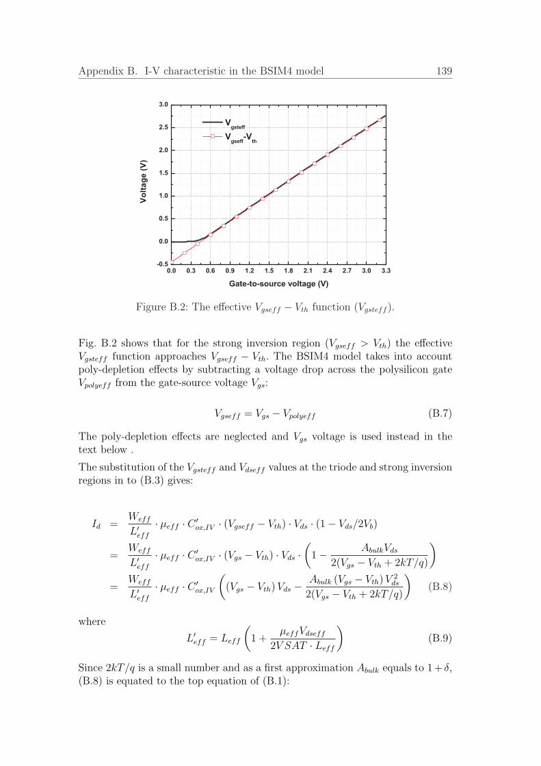
Appendix B. I-V characteristic in the BSIM4 model 139
Figure B.2: The effective Vgseff − Vth function (Vgsteff ).
Fig. B.2 shows that for the strong inversion region (Vgseff > Vth) the effectiveVgsteff function approaches Vgseff − Vth. The BSIM4 model takes into accountpoly-depletion effects by subtracting a voltage drop across the polysilicon gateVpolyeff from the gate-source voltage Vgs:
Vgseff = Vgs − Vpolyeff (B.7)
The poly-depletion effects are neglected and Vgs voltage is used instead in thetext below .
The substitution of the Vgsteff and Vdseff values at the triode and strong inversionregions in to (B.3) gives:
Id =Weff
L′eff
· µeff · C ′ox,IV · (Vgseff − Vth) · Vds · (1− Vds/2Vb)
=Weff
L′eff
· µeff · C ′ox,IV · (Vgs − Vth) · Vds ·
(1− AbulkVds
2(Vgs − Vth + 2kT/q)
)
=Weff
L′eff
· µeff · C ′ox,IV
((Vgs − Vth) Vds − Abulk (Vgs − Vth) V 2
ds
2(Vgs − Vth + 2kT/q)
)(B.8)
where
L′eff = Leff
(1 +
µeffVdseff
2V SAT · Leff
)(B.9)
Since 2kT/q is a small number and as a first approximation Abulk equals to 1+ δ,(B.8) is equated to the top equation of (B.1):

Appendix B. I-V characteristic in the BSIM4 model 140
Id =Weff
L′eff
· µeff · C ′ox,IV
[(Vgs − Vth) Vds − 1
2(1 + δ)V 2
ds
](B.10)
The substitution of the Vgsteff and Vdseff values at the saturation and stronginversion regions in to (B.3) gives:
Id =1
K
Weff
L′eff
· µeff · C ′ox,IV ·
(Vgs − Vth)2
1 + δ(B.11)
where
K =1
(1− Vdseff/2Vb)(B.12)
Figure B.3: K multiplier.
The multiplier K approaches the value of 2 for the long channel devices at thesaturation (see Fig. B.3) that finally transforms (B.11) to the bottom equationof (B.1).

Bibliography
[Agilent 00,a] Agilent, “AN 5968-6875E characterizing digitally modulatedsignals with CCDF curves”, http://www.agilent.com, Januar2000.
[Agilent 00,b] Agilent, “PN 89400-14, using error vector magnitude measure-ments to analyze and troubleshoot vector-modulated signals”,http://www.agilent.com, October 2000.
[Agilent 04] Agilent, “EVM WithRef”, help for ADS2004A, 2004.
[Akkul 04] Mustafa Akkul, Michael Roberts, Vanessa Walker, and Wolf-gang Bosch, “High efficiency power amplifier input/outputcircuit topologies for base station and WLAN applications”,in IEEE MTT-S International Microwave Symposium Digest,pp. 843–846, June 2004.
[Albulet 01] Mihai Albulet, RF power amplifiers, Noble Publishing, firstedition, 2001.
[Aoki 01] Ichiro Aoki, Scott D. Kee, David Rutledge, and Ali Hajimiri,“A 2.4 GHz, 2.2 W, 2 V Fully-integrated CMOS circular-geometry active-transformer power amplifier”, in IEEE Con-ference on Custom Integrated Circuits, pp. 57–60, May 2001.
[Aoki 02,a] Ichiro Aoki, Scott D. Kee, David B. Rutledge, and AliHajimiri, “Distributed active transformer - a new power-combining and impedance-transformation technique”, IEEETransactions on Microwave Theory and Techniques, vol. 50,no. 1, pp. 316–331, January 2002.
[Aoki 02,b] Ichiro Aoki, Scott D. Kee, David B. Rutledge, and Ali Ha-jimiri, “Fully integrated CMOS power amplifier design usingthe distributed active-transformer architecture”, IEEE Jour-nal of Solid-State Circuits, vol. 37, no. 3, pp. 371–383, March2002.
141

Bibliography 142
[Aoki 03] I. Aoki, S. Kee, D. Rutledge, and Ali Hajimiri, “A fully-integrate 1.8 V, 2.9 W, 1.9 GHz, CMOS power amplifier”,in IEEE Radio Frequency Integrated Circuits (RFIC) Sympo-sium, pp. 199–202, June 2003.
[Aparicio 02] R. Aparicio and A. Hajimiri, “Capacity limits and matchingproperties of integrated capacitors”, IEEE Journal of Solid-State Circuits, vol. 37, no. 3, pp. 383–393, March 2002.
[Asbeck 00] Per Asbeck and Carsten Fallesen, “A 29 dBm 1.9 GHz ClassB power amplifier in a digital CMOS process”, in Proceedingsof the 7th IEEE International Conference on Electronics, Cir-cuits and Systems, pp. 474–477, December 2000.
[Bahl 04] Inder J. Bahl, “Low loss matching (LLM) design techniquefor power amplifiers”, IEEE Microwave Magazine, pp. 66–71,December 2004.
[Bakalski 02] W. Bakalski, W. Simbuerger, D. Kehrer, H.D. Wohlmuth,M. Rest, and A.L. Scholtz, “A monolithic 2.45 GHz, 0.56 Wpower amplifier with 45 % PAE at 2.4 V in standard 25 GHzfT Si-Bipolar”, in IEEE International Symposium on Circuitsand Systems, pp. IV–803–IV–806, May 2002.
[Bakalski 03,a] W. Bakalski, N. Ilkov, 0. Demovsek, R. Matz, W. Simbuerger,P. Weger, and A.L. Scholtz, “5-6.5 GHz LTCC power amplifiermodule with 0.3 W at 2.4 V in Si-bipolar”, IEE ElectronicsLetters, vol. 39, no. 4, pp. 375–376, February 2003.
[Bakalski 03,b] W. Bakalski, W. Simbuerger, R. Thueringer, A. Vasylyev, andA. L. Scholtz, “A fully integrated 5.3 GHz, 2.4 V, 0.3 W SiGe-bipolar power amplifier with 50 Ω output”, in Proceedings ofthe 29th European Solid-State Circuits Conference, pp. 561–564, September 2003.
[Bakalski 03,c] Winfried Bakalski, Werner Simbuerger, Ronald Thueringer,Hans-Dieter Wohlmuth, and Arpad L. Scholtz, “A fully inte-grated 4.8-6 GHz power amplifier with on-chip output balunin 38 GHz fT Si-bipolar”, in Proceedings of the 29th EuropeanSolid-State Circuits Conference, pp. 695–698, June 2003.
[Bakalski 03,d] Winfried Bakalski, Andriy Vasylyev, Werner Simbuerger,Ronald Thueringer, Hans-Dieter Wohlmuth, Arpad L. Scholtz,and Peter Weger, “A fully integrated 7-18 GHz power ampli-fier with on-chip output balun in 75 GHz-fT SiGe-bipolar”, inProceedings of the Bipolar/BiCMOS Circuits and TechnologyMeeting, pp. 61–64, September 2003.

Bibliography 143
[Bakalski 04,a] Winfried Bakalski, Krzysztof Kitlinski, Guenter Donig,Boris Kapfelsperger, Christian Kuehn, Carsten Ahrens, Wil-fried Oesterreicher, Wolfgang Auchter, Robert Weigel, andArpad L. Scholtz, “Design of a dual-band wireless LAN SiGe-bipolar power amplifier”, High Frequency Electronics, pp. 18–29, September 2004.
[Bakalski 04,b] Winfried Bakalski, Krzysztof Kitlinski, Guenter Donig, BorisKapfelsperger, Wilfried Oesterreicher, Wolfgang Auchter,Robert Weigel, and Arpad L. Scholtz, “A 5.25 GHz SiGe bipo-lar power amplifier for IEEE 802.11a wireless LAN”, in IEEERadio Frequency Integrated Circuits Symposium, pp. 567–570,June 2004.
[Bakalski 04,c] Winfried Bakalski, Werner Simbuerger, Ronald Thueringer,Andriy Vasylyev, and Arpad L. Scholtz, “A fully integrated5.3 GHz 2.4 V 0.3 W SiGe bipolar power amplifier with 50 Ωoutput”, IEEE Journal of Solid-State Circuits, vol. 39, no. 7,pp. 1006–1014, July 2004.
[Baureis 01] Peter Baureis, Matthias Peter, Heiko Hein, and Frank Oehler,“Design procedure for fully integrated 900 MHz mediumpower amplifiers in 0.6 µm CMOS technology on latchup resis-tant EPI-substrate”, in Topical Meeting on Silicon MonolithicIntegrated Circuits in RF Systems, Digest of Papers, pp. 142–148, September 2001.
[Behtash 04,a] R. Behtash, H. Tobler, F.-J. Berlec, V. Ziegler, H. Leier,R.S. Balmer, T. Martin, M. Neuburger, and H. Schumacher,“Coplanar AlGaN/GaN HEMT power amplifier MMIC at X-band”, in IEEE MTT-S International Microwave SymposiumDigest, pp. 1657–1659, June 2004.
[Behtash 04,b] R. Behtash, H. Tobler, F.-J. Berlec, V. Ziegler, H. Leier,R.S. Balmer, T. Martin, M. Neuburger, and H. Schumacher,“MMIC power amplifier based on AlGaN/GaN HEMTs at10 GHz”, IEE Electronics Letters, vol. 40, no. 9, April 2004.
[Bischof 01] Werner Bischof, Martin Alles, Stephan Gerlach, Achim Kruck,Andreas Schuppen, Joachim Sinderhauf, and Hans-JoachimWassener, “SiGe-power amplifiers in flipchip and packagedtechnology”, in IEEE Radio Frequency Integrated Circuits(RFIC) Symposium, Digest of Papers, pp. 35–38, May 2001.
[Carrara 02,a] Francesco Carrara, Alessandro Castorina, Antonino Scuderi,and Giuseppe Palmisano, “High performance silicon bipolar

Bibliography 144
power amplifier for 1.8 GHz applications”, in IEEE MTT-SInternational Microwave Symposium Digest, pp. 1015–1018,June 2002.
[Carrara 02,b] Francesco Carrara, Antonino Scuderi, Tonio Biondi, andGiuseppe Palmisano, “A 1.8 GHz high-efficiency 34 dBmsilicon bipolar power amplifier”, IEEE Transactions on Mi-crowave Theory and Techniques, vol. 50, no. 12, pp. 2963–2970, December 2002.
[Cartalade 98] David Cartalade, Patrice Senn, Denis Pache, and ErnestoPerea, “An integrated 2 GHz 20 dBm 3 V wide band dif-ferential power amplifier with microstrip antenna interface”,in URSI International Symposium on Signals, Systems, andElectronics, pp. 456–459, October 1998.
[Chan 99] W.C. Chan, Philip K.T. Mok, Johnny K.O. Sin, and W.T.Ng, “Design of monolithic RF power amplifier using bulkBiCMOS process”, in 42nd Midwest Symposium on Circuitsand Systems, pp. 10–13, August 1999.
[Chee 04] Y. H. Chee, J. Rabaey, and A. M. Niknejad, “A Class A/B lowpower amplifier for wireless sensor networks”, in Proceedingsof the International Symposium on Circuits and Systems, pp.IV – 409–12, May 2004.
[Chen 00] Y.J.E. Chen, M. Hamai, D. Heo, A. Sutono, S. Yoo, andJ. Laskar, “RF power amplifier integration in CMOS technol-ogy”, in IEEE MTT-S International Microwave SymposiumDigest, pp. 545–548, June 2000.
[Chen 01] Y. Emery Chen, Yong Kyu. Yoon, Joy Laskar, and MarkAllen, “A 2.4 GHz integrated CMOS power amplifier withmicromachined inductors”, in IEEE MTT-S International Mi-crowave Symposium Digest, pp. 523–526, May 2001.
[Chu 04] C.K. Chu, H.K. Huang, H.Z. Liu, R.J. Chiu, C.H. Lin, C.C.Wang, Y.H. Wang, C.C. Hsu, W. Wu, C.L. Wu, and C.S.Chang, “A fully matched 8 W X-band PHEMT MMIC highpower amplifier”, in IEEE Compound Semiconductor Inte-grated Circuit Symposium, pp. 137–140, October 2004.
[Chung 04] Younkyu Chung, Yuanxun Wang, Dal Ahn, and Tatsuo Itoh,“Efficiency-enhancing technique: LDMOS power amplifier us-ing dual-mode operation design approach”, in IEEE MTT-S International Microwave Symposium Digest, pp. 859–862,June 2004.

Bibliography 145
[Deng 04] Junxiong Deng, Prasad Gudem, Lawrence E. Larson, and Pe-ter M. Asbeck, “A high-efficiency SiGe BiCMOS WCDMApower amplifier with dynamic current biasing for improvedaverage efficiency”, in IEEE Radio Frequency Integrated Cir-cuits Symposium, pp. 361–364, June 2004.
[Deng 05] Junxiong Deng, Prasad S. Gudem, Lawrence E. Larson, andPeter M. Asbeck, “A high average-efficiency SiGe HBT poweramplifier for WCDMA handset applications”, IEEE Transac-tions on Microwave Theory and Techniques, vol. 53, no. 2, pp.529–537, February 2005.
[Ding 04] Yongwang Ding and Ramesh Harjani, “A CMOS high effi-ciency +22 dBm linear power amplifier”, in Proceedings ofthe IEEE Custom Integrated Circuits Conference, pp. 557–560, October 2004.
[Dow 04] G. Samuel Dow, Richard Ho, Matthew Chin, and Mark Yu,“Low DC current 2.4-2.5 GHz and 4.9-6.0 GHz linear poweramplifier modules for IEEE 802.11a/b/g applications”, inIEEE Radio Frequency Integrated Circuits (RFIC) Sympo-sium, Digest of Papers, pp. 75–78, June 2004.
[Eccleston 04] K.W. Eccleston and O. Kyaw, “Analysis and design of class-B dual fed distributed power amplifiers”, IEE Proceedings ofMicrowaves, Antennas and Propagation, vol. 151, no. 2, pp.104–108, April 2004.
[Ellinger 05] Frank Ellinger, “60 GHz SOI travelling-wave amplifier withNF Below 3.8 dB from 0.1 to 40 GHz”, IEEE Journal of Solid-State Circuits, vol. 40, no. 2, pp. 553–558, February 2005.
[Ellis 04] Grant A. Ellis, Ara Kurdoghlian, Ross Bowen, Mike Wetzel,and Mike Delaney, “W-band InP DHBT MMIC power ampli-fiers”, in IEEE MTT-S International Microwave SymposiumDigest, pp. 231–234, June 2004.
[Eo 04,a] YunSeong Eo and KwangDu Lee, “A 2.4 GHz/5.2 GHz CMOSpower amplifier for dual-band applications”, in IEEE MTT-SInternational Microwave Symposium Digest, pp. 1539–1542,June 2004.
[Eo 04,b] YunSeong Eo and KwangDu Lee, “A fully integrated 24 dBmCMOS power amplifier for 802.11a WLAN applications”,IEEE Microwave and Wireless Components Letters, vol. 14,no. 11, pp. 504–506, November 2004.

Bibliography 146
[Eo 04,c] YunSeong Eo and KwangDu Lee, “High efficiency 5 GHzCMOS power amplifier with adaptive bias control circuit”,in IEEE Radio Frequency Integrated Circuits Symposium, pp.575–578, June 2004.
[Erben 95] U. Erben, M. Wahl, A. Schueppen, and H. Schumacher,“Class-A SiGe HBT power amplifiers at C-band frequencies”,IEEE Microwave and Guided Wave Letters, vol. 5, no. 12, pp.435–436, December 1995.
[Fallesen 01,a] Carsten Fallesen and Per Asbeck, “A 1 W 0.35 µm CMOSpower amplifier for GSM-1800 with 45 % PAE”, in IEEEInternational Solid-State Circuits Conference, Digest of Tech-nical Papers, pp. 158–159, February 2001.
[Fallesen 01,b] Carsten Fallesen and Per Asbeck, “A 1 W CMOS Power am-plifier for GSM-1800 with 55 % PAE”, in IEEE MTT-S In-ternational Microwave Symposium Digest, pp. 911–914, May2001.
[Fortes 01] Fernando Fortes and Maria Jo ao do Rosario, “A second har-monic Class-F power amplifier in standard CMOS technol-ogy”, IEEE Transactions on Microwave Theory and Tech-niques, vol. 49, no. 6, pp. 1216–1220, June 2001.
[Fujii 04] Kohei Fujii and Henrik Morkner, “1W power amplifier MMICsfor mm-wave applications”, in IEEE MTT-S InternationalMicrowave Symposium Digest, pp. 1665–1668, June 2004.
[Fukuda 04] Atsushi Fukuda, Hiroshi Okazaki, Tetsuo Hirota, and YasushiYamao, “Novel 900 MHz/1.9 GHz dual-mode power amplifieremploying MEMS switches for optimum matching”, IEEEMicrowave and Wireless Components Letters, vol. 14, no. 3,pp. 121–123, March 2004.
[Giry 00] A. Giry, J-M. Fournier, and M. Pons, “A 1.9 GHz low voltageCMOS power amplifier for medium power rf applications”,in IEEE Radio Frequency Integrated Circuits (RFIC) Sympo-sium, Digest of Papers, pp. 121–124, June 2000.
[Gonzalez 97] Guillermo Gonzalez, Microwave transistor amplifiers analysisand design, Prentice Hall, second edition, 1997.
[Gray 01] Gray, Hurst, Lewis, and Meyer, Analysis and design of analogintegrated circuits, John Wiley & Sons, fourth edition, 2001.

Bibliography 147
[Grewing 04] Christian Grewing, Kay Winterberg, Stefan van Waasen, Mar-tin Friedrich, Giuseppe Li Puma, Andreas Wiesbauer, andChristoph Sandner, “Fully integrated distributed power am-plifier in CMOS technology, optimized for UWB transmit-ters”, in Radio Frequency Integrated Circuits (RFIC) Sym-posium, Digest of Papers, pp. 87–90, June 2004.
[Grover 46] Frederick W. Grover, Inductance calculations working formu-las and tables, Instrument Society of America, first edition,1946.
[Gruendlingh 04] Johan Gruendlingh, Kevin Parker, and Gordon Rabjohn, “Ahigh efficiency Chireix out-phasing power amplifier for 5 GHzWLAN applications”, in IEEE MTT-S International Mi-crowave Symposium Digest, pp. 1535–1538, June 2004.
[Gupta 98] Ravi Gupta and David J. Allstot, “Parasitic-aware de-sign and optimization of CMOS RF integrated circuits”, inIEEE MTT-S International Microwave Symposium Digest,pp. 1867–1870, June 1998.
[Gupta 01] Ravi Gupta, Brian M. Ballweber, and David J. Allstot, “De-sign and optimization of CMOS RF power amplifiers”, IEEEJournal of Solid-State Circuits, vol. 36, no. 2, pp. 166–175,February 2001.
[Hamedi-Hagh 03] Sotoudeh Hamedi-Hagh and C. Andre T.Salama, “A 1 V,8 GHz CMOS integrated phase shifted transmitter for wide-band and varying envelope communication systems”, in IEEECustom Integrated Circuits Conference, pp. 447–450, October2003.
[Heinz 00] Alexander Heinz, Werner Simbuerger, Hans-DieterWohlmuth, Peter Weger, Wilhelm Wilhelm, ReinhardGabl, and Klaus Aufinger, “A monolithic 2.8 V, 3.2 W siliconbipolar power amplifier with 54 % PAE at 900 MHz”, in IEEERadio Frequency Integrated Circuits (RFIC) Symposium,Digest of Papers, pp. 117–120, June 2000.
[Hella 01] Mona M. Hella and Mohammed Ismail, “A digitally controlledCMOS RF power amplifier”, in Proceedings of the 44th IEEEMidwest Symposium on Circuits and Systems, pp. 833–835,August 2001.
[Hella 02] M.M. Hella and M. Ismail, “2 GHz controllable power ampli-fier in standard CMOS process for short-range wireless appli-cations”, IEE Proceedings of Circuits, Devices and Systems,vol. 149, no. 56, pp. 363–368, October 2002.

Bibliography 148
[Heo 01] D. Heo, A. Sutono, E. Chen, Y. Suh, and J. Laskar, “A1.9 GHz DECT CMOS power amplifier with fully integratedmultilayer LTCC passives”, IEEE Microwave and WirelessComponents Letters, vol. 11, no. 6, pp. 249–251, June 2001.
[Ho 02] K. W. Ho and H. C. Luong, “A 1 V CMOS power amplifierfor Bluetooth application”, in 45th Midwest Symposium onCircuits and Systems, pp. II–457 – II–460, August 2002.
[Ho 03] Ka-Wai Ho and Howard C. Luong, “A 1 V CMOS poweramplifier for bluetooth applications”, IEEE Transactions onCircuits and SystemsII: Analog and Digital Signal Processing,vol. 50, no. 8, pp. 445–449, August 2003.
[Hsiao 01] Chao-Chih Hsiao, Chin-Wei Kuo, and Yi-Jen Chan, “Inte-grated CMOS power amplifier and down-converter for 2.4 GHzBluetooth applications”, in Radio and Wireless Conference,pp. 29–32, August 2001.
[Hung 03] Tang Tat Hung and Mourad N. El-Gamal, “Class-E CMOSpower amplifiers for RF applications”, in Proceedings of theInternational Symposium on Circuits and Systems, pp. I–449–I–452, May 2003.
[Johnson 04] Jeffrey B. Johnson, Alvin J. Joseph, David C. Sheridan, Ra-mana M. Maladi, Per-Olof Brandt, Jonas Persson, Jesper An-dersson, Are Bjorneklett, Ulrika Persson, Fariborz Abasi, andLars Tilly, “Silicon-germanium BiCMOS HBT technology forwireless power amplifier applications”, IEEE Journal of Solid-State Circuits, vol. 39, no. 10, pp. 1605–1614, October 2004.
[Juurakko 03] Pasi Juurakko, Ville Saari, Jussi Ryynanen, and Kari Halo-nen, “Differential SiGe power amplifier for 3GPP WCDMA”,in IEEE Radio Frequency Integrated Circuits (RFIC) Sympo-sium, pp. 133–136, June 2003.
[Kenington 02] Peter B. Kenington, High-linearity RF amplifier design,Arthech House, first edition, 2002.
[Khannur 03] Pradeep B. Khannur, “A CMOS power amplifier with powercontrol and T/R switch for 2.45 GHz Bluetooth/ISM bandapplications”, in Radio Frequency Integrated Circuits (RFIC)Symposium, pp. 145–148, June 2003.
[Kim 01] Jonghae Kim, Bradford Palmel, and Ramesh Harjani, “Ahigh efficiency +20 dBm, 900 MHz power amplifier modulein 0.35 µm CMOS”, in IEEE Radio and Wireless Conference,pp. 149–152, August 2001.

Bibliography 149
[Kitlinski 04] Krzysztof Kitlinski, Guenter Donig, Boris Kapfelsperger, andRobert Weigel, “Si-Ge power amplifier for WCDMA hand-held applications”, in 15th International Conference on Mi-crowaves, Radar and Wireless Communications, pp. 203–206,September 2004.
[Komijani 04] Abbas Komijani and Ali Hajimiri, “A 24 GHz, +14.5 dBmfully-integrated power amplifier in 0.18 µm CMOS”, in Pro-ceedings of the IEEE Custom Integrated Circuits Conference,pp. 561–564, October 2004.
[Kunihiro 04] Kazuaki Kunihiro, Shingo Yamanouchi, Takashi Miyazaki,Yuuichi Aoki, Kazuhiro Ikuina, Takashi Ohtsuka, and HikaruHida, “A diplexer-matching dual-band power amplifier LTCCmodule for IEEE 802.11a/b/g wireless LANs”, in IEEE Ra-dio Frequency Integrated Circuits (RFIC) Symposium, Digestof Papers, pp. 303–306, June 2004.
[Kuo 01] Timothy C. Kuo and Bruce B. Lusignan, “A 1.5 W Class-FRF power amplifier in 0.2 µm CMOS technology”, in IEEEConference on Custom Integrated Circuits, pp. 154–155, May2001.
[Liu 01] William Liu, MOSFET models for SPICE simulation, includ-ing BSIM3v3 and BSIM4, John Wiley & Sons, first edition,2001.
[Luo 01,a] Sifen Luo and Tirdad Sowlati, “A monolithic SI PCS-CDMA power amplifier with an impedance-controllable bi-asing scheme”, in IEEE Radio Frequency Integrated Circuits(RFIC) Symposium, Digest of Papers, pp. 217–220, May 2001.
[Luo 01,b] Sifen Luo and Tirdad Sowlati, “A monolithic Si PCSCDMApower amplifier with 30 % PAE at 1.9 GHz using a novelbiasing scheme”, IEEE Transactions on Microwave Theoryand Techniques, vol. 49, no. 9, pp. 1552–1557, September 2001.
[March 91] Steven L. March, “Simple equations characterize bond wires”,Microwaves & RF, pp. 105–110, November 1991.
[Mertens 02] Koen L. R. Mertens and Michiel S. J. Steyaert, “A 700 MHz1 W fully differential CMOS Class-E power amplifier”, IEEEJournal of Solid-State Circuits, vol. 37, no. 2, pp. 137–141,February 2002.
[Noh 04] Youn S. Noh, Ji H. Kim, Jong H. Park, and C.S. Park,“A 3.3 V operation single HBT power amplifier MMIC For

Bibliography 150
2.4 GHz/5GHz dual-band WLAN applications”, in IEEE Ra-dio and Wireless Conference, pp. 483–486, September 2004.
[Ooi 04] Shirt Fun Ooi, Steven Gao, A. Sambell, D. Smith, and P. But-terworth, “High efficiency class-F power amplifier design”, inHigh Frequency Postgraduate Student Colloquium, pp. 113–118, September 2004.
[OSullivan 03] J.A. OSullivan, C. Delabie, K. G. McCarthy, A. Murphy, andP.J. Murphy, “A fully integrated high efficiency SiGe HBTClass F power amplifier at 2.2 GHz”, in High Frequency Post-graduate Student Colloquium, pp. 48–51, September 2003.
[Paidi 05] Vamsi K. Paidi, Zach Griffith, Yun Wei, Mattias Dahlstrom,Miguel Urteaga, Navin Parthasarathy, Munkyo Seo, LoreneSamoska, Andy Fung, and Mark J.W. Rodwell, “G-Band(140220 GHz) and W -Band (75110 GHz) InP DHBT MediumPower Amplifiers”, IEEE Transactions on Microwave Theoryand Techniques, vol. 53, no. 2, pp. 598–504, February 2005.
[Pfeiffer 04] Ullrich R. Pfeiffer, Scott K. Reynolds, and Brian A. Floyd, “A77 GHz SiGe power amplifier for potential applications in au-tomotive radar systems”, in IEEE Radio Frequency IntegratedCircuits Symposium, pp. 91–94, June 2004.
[Point 03] Robert Point, Zhenbiao Li, and etc., “An RF CMOS trans-mitter integrating a power amplifier and a transmit/receiveswitch for 802.11b wireless local area network applications”,in Radio Frequency Integrated Circuits (RFIC) Symposium,pp. 431–434, June 2003.
[Raab 77] Frederick H. Raab, “Idealized operation of the Class E tunedpower amplifier”, IEEE Transactions on Circuits and Sys-tems, vol. 24, no. 12, pp. 725–735, December 1977.
[Raab 01] Frederick H. Raab, “Maximum efficiency and output of Class-F power amplifiers”, IEEE Transactions on Microwave The-ory and Techniques, vol. 49, no. 6, pp. 1162–1166, June 2001.
[Raghavan 02] Arvind Raghavan, Deukhyoun Heo, Moonkyun Maengl, Al-bert Sutono, Kyutae Lim, and Joy Laskarl, “A 2.4 GHz highefficiency SiGe HBT power amplifier with high-Q LTCC har-monic suppression filter”, in IEEE MTT-S International Mi-crowave Symposium Digest, pp. 1019–1022, June 2002.
[Razavi 98] Behzad Razavi, RF microelectronics, Prentice Hall, first edi-tion, 1998.

Bibliography 151
[Rippke 03] Ian Rippke, Jon Duster, and Kevin Kornegay, “A fully inte-grated, single-chip handset power amplifier in SiGe BiCMOSfor W-CDMA applications”, in IEEE Radio Frequency Inte-grated Circuits (RFIC) Symposium, pp. 667–670, June 2003.
[Rofougaran 94] M. Rofougaran, A. Rofougaran, C. Olgaard, and A. A. Abidi,“A 900 MHz CMOS RF power amplifier with programmableoutput”, in Symposium on VLSI Circuits, Digest of TechnicalPapers, pp. 133–134, JUNE 1994.
[Samoska 04] Lorene Samoska, Alejandro Peralta, Ming Hu, Miro Micovic,and Adele Schmitz, “A 20 mW, 150 GHz InP HEMT MMICpower amplifier module”, IEEE Microwave and WirelessComponents Letters, vol. 14, no. 2, pp. 56–58, February 2004.
[Schroeter 05] Michael Schroeter and Anjan Chakravorty, “HICUM a geome-try scalable physics-based compact bipolar transistor model”,Documentation of model level 2 version 2.2, August 2005.
[Scuderi 03] Antonino Scuderi, Francesco Carrara, Alessandro Castorina,and Giuseppe Palmisano, “A high performance RF poweramplifier with protection against load mismatches”, in IEEEMTT-S International Microwave Symposium Digest, pp. 699–702, June 2003.
[Scuderi 04,a] Angelo Scuderi, Antonino Scuderi, Francesco Carrara, andGiuseppe Palmisano, “VSWR-protected silicon bipolar poweramplifier with smooth power control slope”, in IEEE Interna-tional Solid-State Circuits Conference, pp. 194–522, February2004.
[Scuderi 04,b] Antonino Scuderi, Francesco Carrara, and GiuseppePalmisano, “A 5.2 GHz silicon bipolar power amplifierfor IEEE 802.11a and HIPERLAN2 wireless LANs”, in Pro-ceedings of the 30th European Solid-State Circuits Conference,pp. 203–206, September 2004.
[Scuderi 04,c] Antonino Scuderi, Domenico Cristaudo, Francesco Carrara,and Giuseppe Palmisano, “A high performance siliconbipolar monolithic RF linear power amplifier for W-LANIEEE802.11g applications”, in IEEE Radio Frequency Inte-grated Circuits (RFIC) Symposium, pp. 79–82, June 2004.
[Scuderi 05] Angelo Scuderi, Luca La Paglia, Antonino Scuderi, FrancescoCarrara, and Giuseppe Palmisano, “A VSWR-protected sili-con bipolar rf power amplifier with soft-slope power control”,

Bibliography 152
IEEE Journal of Solid-State Circuits, vol. 40, no. 3, pp. 611–621, March 2005.
[Shinjo 03] Shintaro Shinjo, Hiro omi Ueda, Takayuki Sugano, andMasahiko Nakanishi, “High P1dB and low quiescent currentSiGe HBT power amplifier MMIC using self base bias con-trol circuit for 5.8 GHz ETC terminals”, in IEEE Radio Fre-quency Integrated Circuits (RFIC) Symposium, pp. 195–198,June 2003.
[Shirvani 01] Alireza Shirvani, David K. Su, and Bruce A. Wooley, “ACMOS RF power amplifier with parallel amplification for ef-ficient power control”, in IEEE International Solid-State Cir-cuits Conference, Digest of Technical Papers, pp. 156–157,442,February 2001.
[Shirvani 02] Alireza Shirvani, David K. Su, and Bruce A. Wooley, “ACMOS RF power amplifier with parallel amplification for ef-ficient power control”, IEEE Journal of Solid-State Circuits,vol. 37, no. 6, pp. 684–693, June 2002.
[Simbuerger 96] W. Simbuerger, H.P. Trost, H. D. Wohlmuth, H. Knapp, andP. Weger, “1.3 W 1.9 GHz and 1 W 2.4 GHz power amplifierMMIC in silicon”, IEE Electronics Letters, vol. 32, no. 19, pp.1827–1829, September 1996.
[Simbuerger 99,a] Wener Simbuerger, Hans-Dieter Wohlmuth, Peter Weger, andAlexander Heinz, “A monolithic transformer coupled 5 Wsilicon power amplifier with 59 % PAE at 0.9 GHz”, IEEEJournal of Solid-State Circuits, vol. 34, no. 12, pp. 1881–1892,December 1999.
[Simbuerger 99,b] Werner Simbuerger, Hans-Dieter Wohlmuth, and PeterWeger, “A monolithic 3.7 W silicon power amplifier with 59 %PAE at 0.9 GHz”, in IEEE International Solid-state CircuitsConference, pp. 230–231, February 1999.
[Simbuerger 00] Werner Simbuerger, Alexander Heinz, Hans-DieterWohlmuth, Josef Boeck, Klaus Aufinger, and MirjanaRest, “A monolithic 2.5 V, 1 W silicon bipolar poweramplifier with 55 % PAE at 1.9 GHz”, in IEEE MTT-SInternational Microwave Symposium Digest, pp. 853–856,June 2000.
[Sokal 75] Nathan O. Sokal and Alan D. Sokal, “Class E-A new classof high-efficiency tuned single-ended switching power ampli-fiers”, IEEE Journal of Solid-State Circuits, vol. 10, no. 3, pp.168–176, June 1975.

Bibliography 153
[Sowlati 02] Tirdad Sowlati and Domine Leenaerts, “A 2.4 GHz 0.18 µmCMOS self-biased cascode power amplifier with 23 dBm out-put power”, in IEEE International Solid-State Circuits Con-ference, Digest of Technical Papers, pp. 294 – 467, February2002.
[Sowlati 03] Tirdad Sowlati and Domine M. W. Leenaerts, “A 2.4 GHz0.18 µm CMOS self-biased cascode power amplifier”, IEEEJournal of Solid-State Circuits, vol. 38, no. 8, pp. 1318–1324,August 2003.
[Su 97] David Su and William McFarland, “A 2.5 V, 1 W monolithicCMOS RF power amplifier”, in Proceedings of the IEEE Cus-tom Integrated Circuits Conference, pp. 189–192, May 1997.
[Suematsu 01] Noriharu Suematsu and Shintaro Shinjo, “CMOS/BiCMOSpower amplifier technology trend in Japan”, in Gallium Ar-senide Integrated Circuit (GaAs IC) Symposium, 23rd AnnualTechnical Digest, pp. 107–110, October 2001.
[Sutono 00] A. Sutono, D. Heo, E. Chen, K. Lim, and J. Laskar, “Compactimplementation of component library in LTCC technology andits application to CMOS RF power amplifier design”, in Pro-ceedings of the IEEE Conference on Electrical Performance ofElectronic Packaging, pp. 288–291, October 2000.
[Tanzi 03] Nebil Tanzi, Jeff Dykstra, and Ken Hutchinson, “A 1-Wattdoubly balanced 5 GHz flip-chip SiGe power amplifier”, inIEEE Radio Frequency Integrated Circuits (RFIC) Sympo-sium, pp. 141–144, June 2003.
[Thueringer 03] Ronald Thueringer, Marc Tiebout, Werner Simbuerger,Christoph Kienmayer, and Arpad L. Scholtz, “A 17 GHzlinear 50 Ω output driver in 0.12 µm standard CMOS”, inRadio Frequency Integrated Circuits (RFIC) Symposium, pp.207–210, June 2003.
[Toner 04] B. Toner, R. Dharmalinggam, and V.F. Fusco, “5.5 GHz802.11a 0.18 µm CMOS pre-power amplifier core with on-chiplinearization”, IEE Proceedings of Microwaves Antennas andPropagation, vol. 151, no. 1, pp. 26–30, February 2004.
[Trost 97] H. P. Trost, W. Simbuerger, H. D. Wohlmuth, H. Knapp,P. Weger, and A. L. Scholtz, “1.6 Watt 1.9 GHz power ampli-fier MMIC in silicon”, in IEE Colloquium RF and MicrowaveCircuits for Commercial Wireless Applications, pp. 4–1–4–5,February 1997.

Bibliography 154
[Tsai 99] King-Chun Tsai and Paul R. Gray, “A 1.9 GHz, 1 W CMOSClass-E power amplifier for wireless communications”, IEEEJournal of Solid-State Circuits, vol. 34, no. 7, pp. 962–970,July 1999.
[Tseng 00] Pei-Der Tseng, Liyang Zhang, Guang-Bo Gao, Senior Mem-ber, and M. Frank Chang, “A 3 V monolithic SiGe HBT poweramplifier for dual-mode (CDMA/AMPS) cellular handset ap-plications”, IEEE Journal of Solid-State Circuits, vol. 35, no.9, pp. 1338–1344, September 2000.
[Tu 04] Steve Hung-Lung Tu, “Class E RF tuned power amplifiers inCMOS technologies: theory and circuit design considerations”,IEEE Communications Magazine, vol. 42, no. 9, pp. S6–S11,September 2004.
[Upshur 04] J.T. Upshur, C. White, M.E. Bayne, B. Davis, L. Walker,M.A. Reece, W.L. Thompson, S. Cheng, and R.E. Wal-lis, “Advanced non-linear model for accurate prediction ofharmonically terminated power amplifier performance”, inIEEE MTT-S International Microwave Symposium Digest,pp. 1075–1078, June 2004.
[Vasylyev 04] A. Vasylyev, P. Weger, W. Bakalski, R. Thueringer, andW. Simbuerger, “A monolithic 2.4 GHz, 0.13 µm CMOS poweramplifier with 28 dBm output power and 48 % PAE at 1.2 Vsupply”, in Proceedings of 14th International Crimean Con-ference, Microwave and Telecommunication Technology, pp.98–99, September 2004.
[Vasylyev 05,a] A. Vasylyev, Peter Weger, and Werner Simbuerger, “Ultra-broadband 20.5-31 GHz monolithically integrated CMOSpower amplifier”, IEE Electronics Letters, vol. 41, no. 23,pp. 1281–1282, November 2005.
[Vasylyev 05,b] Andriy Vasylyev, Peter Weger, Winfried Bakalski, and WernerSimbuerger, “Fully-integrated 32 dBm, 1.52.9 GHz SiGe-bipolar power amplifier using power-combining transformer”,IEE Electronics Letters, vol. 41, no. 16, pp. 908–909, August2005.
[Vasylyev 06] Andriy V. Vasylyev, Peter Weger, Winfried Bakalski, andWerner Simbuerger, “17 GHz 50-60 mW power amplifiersin 0.13 µm standard CMOS”, IEEE Microwave and WirelessComponents Letters, vol. 16, no. 1, pp. 37–39, January 2006.

Bibliography 155
[Wang 01] Chengzhou Wang, Lawrence E. Larson, and Peter M. Asbeck,“A nonlinear capacitance cancellation technique and its appli-cation to a CMOS Class AB power amplifier”, in IEEE RadioFrequency Integrated Circuits (RFIC) Symposium, Digest ofPapers, pp. 39–42, May 2001.
[Wang 04,a] Chengzhou Wang, Mani Vaidyanathan, and Lawrence E. Lar-son, “A capacitance-compensation technique for improved lin-earity in CMOS Class-AB power amplifiers”, IEEE Journal ofSolid-State Circuits, vol. 39, no. 11, pp. 1927–1937, November2004.
[Wang 04,b] Narisi Wang, Vahid Yousefzadeh, Dragan Maksimovic, SrdjanPajic, and Zoya B. Popovic, “60 % efficient 10-GHz poweramplifier with dynamic drain bias control”, IEEE Transac-tions on Microwave Theory and Techniques, vol. 52, no. 3, pp.1077–1081, March 2004.
[Wang 04,c] Wei Wang and Y. P. Zhang, “0.18 µm CMOS push-pull poweramplifier with antenna in IC package”, IEEE Microwave andWireless Components Letters, vol. 14, no. 1, pp. 13–15, Jan-uary 2004.
[Wei 00] C. J. Wei, P. DiCarlo, Y. A. Tkachenko, R. McMorrow, andD. Bartle, “Analysis and experimental waveform study on in-verse Class Class-F mode of microwave power FETs”, in IEEEMTT-S International Microwave Symposium Digest, pp. 525–528, June 2000.
[Wong 96] S. L. Wong, H. Bhimnathwala, S. Luo, B. Halali, and S. Navid,“A 1 W 830 MHz monolithic BiCMOS power amplifier”, inIEEE International Solid-State Circuits Conference, pp. 52–53,416, February 1996.
[Yamamoto 01] Kazuya Yamamoto, Tetsuya Heima, Akihiko Furukawa,Masayoshi Ono, Yasushi Hashizume, Hiroshi Komurasaki,Shigenobu Maeda Hisayasu Sato, and Naoyuki Kato, “A2.4 GHz-Band 1.8 V operation single-chip Si-CMOS T/R-MMIC front-end with a low insertion loss switch”, IEEEJournal of Solid-State Circuits, vol. 36, no. 8, pp. 1186–1197,August 2001.
[Yamamoto 04] K. Yamamoto, S. Suzuki, N. Ogawa, T. Shimra, and K. Maen-wra, “InGaP/GaAs HBT MMICs for 5-GHz-band wirelessapplications a high P1dB, 23/4-dB step-gain low-noise ampli-fier and a power amplifier”, in IEEE MTT-S InternationalMicrowave Symposium Digest, pp. 551–554, June 2004.

Bibliography 156
[Yen 03] Cheng-Chi Yen and Huey-Ru Chuang, “A 0.25 µm 20 dBm2.4 GHz CMOS power amplifier with an integrated diode lin-earizer”, IEEE Microwave and Wireless Components Letters,vol. 13, no. 2, pp. 45–47, February 2003.
[Yoo 00] Changsik Yoo and Qiuting Huang, “A common-gate switched,0.9 W Class-E Power amplifier with 41 % PAE in 0.25 µmCMOS”, in Symposium on VLSI Circuits, Digest of TechnicalPapers, pp. 56–57, June 2000.
[Yoo 01] Changsik Yoo and Qiuting Huang, “A common-gate switched0.9 W Class-E power amplifier with 41 % PAE in 0.25 µmCMOS”, IEEE Journal of Solid-State Circuits, vol. 36, no. 5,pp. 823–830, May 2001.
[Ytterdal 03] Trond Ytterdal, Yuhua Cheng, and Tor Fjeldly, Device mod-elling for analog and RF CMOS circuit design, John Wiley &Sons, first edition, 2003.
[Zhang 00] Xiangdong Zhang, Chone Saycocie, Scott Munro, and GregoryHenderson, “A SiGe HBT power amplifier with 40 % PAE forPCS CDMA applications”, in IEEE MTT-S InternationalMicrowave Symposium Digest, pp. 857–860, June 2000.
[Zhang 03] Xuejun Zhang, Design of linear RF outphasing power ampli-fiers, Artech House, first edition, 2003.
[Zhang 04] Ying Zhang and Payam Heydari, “A novel linearization tech-nique for linear/pseudo-linear RF CMOS power amplifiers”,in Digest of Papers of Radio Frequency Integrated Circuits(RFIC) Symposium, pp. 563–566, June 2004.