independent input and output common-mode controlsbosa51
TRANSCRIPT

THS4567 220 MHz, High Input Impedance, Fully Differential Amplifier withIndependent Input and Output Common-Mode Control
1 Features• Gain Bandwidth Product (GBWP): 220 MHz• Slew Rate: 500 V/µs• Bandwidth: 42 MHz (G = 10 V/V)• Voltage Noise: 4.2 nV/√ Hz• Supply Current (IQ): 2 mA• IQ : 28 µA (Shutdown)• Rail-to-Rail Output (RRO)• High Impedance CMOS Inputs• Independent Input and Output Common-Mode
Control• Disable Input Common-Mode Loop to Use as a
Standard Fully Differential Amplifier (FDA)• Single-Supply Range: 3.3 V to 5.5 V• Split-Supply Range: ±1.65 V to ±2.75 V• Operating Temperature Range: -40°C to 125°C
2 Applications• Absolute Optical Encoder• AC Drive Position Feedback• Linear Motor Position Sensor• Clinical Pulse Oximeter• Optical Coherence Tomography
3 DescriptionThe THS4567 device is a novel fully-differentialamplifier (FDA) that includes independent inputcommon-mode (VICM) and output-common mode(VOCM) control. Standard FDAs only possess outputcommon-mode control. The THS4567 is adecompensated amplifier with a minimum stable gainof 10 V/V.
The THS4567 operates as a fully differentialtransimpedance amplifier (TIA) and analog-to-digitalconverter (ADC) driver in a single integrated stage.
The VICM loop decouples the reverse bias across thephotodiode(PD) from the amplifiers input and outputswing compliance ranges thereby allowing thedesigner to maximize the PD reverse bias andminimize the PD capacitance. The VICM loop can bedisabled which then allows the THS4567 to operateas a standard FDA.
The VOCM loop sets the differential output common-mode voltage and is typically set at the subsequentADC stage common-mode reference voltage.
Device Information (1)
PART NUMBER PACKAGE BODY SIZE (NOM)THS4567 WQFN (10) 2.00 mm × 2.00 mm
(1) For all available packages, see the package optionaddendum at the end of the data sheet.
+
±
±
+
1 M
0.8 pF
1 M
0.8 pF
5 V
VOCM = 2.5 VVICM = 1.5 V
3.3
3.3
ADC1 nF
VBIAS
VBIAS
0.1 F 0.1 F
0.1 F
Single-Stage Differential-Input to Differential-Output, TIA and ADC Driver for Optical Encoders
Frequency (Hz)
Norm
aliz
ed G
ain
(dB
)
-12
-9
-6
-3
0
3
1M 10M 100M
D201
G = 7 V/VG = 10 V/VG = 40 V/VG = 100 V/V
Small-Signal Frequency Response vs Gain
www.ti.comTHS4567
SBOSA51 – DECEMBER 2020
Copyright © 2020 Texas Instruments Incorporated Submit Document Feedback 1
Product Folder Links: THS4567
THS4567SBOSA51 – DECEMBER 2020
An IMPORTANT NOTICE at the end of this data sheet addresses availability, warranty, changes, use in safety-critical applications,intellectual property matters and other important disclaimers. PRODUCTION DATA.
Table of Contents1 Features............................................................................12 Applications..................................................................... 13 Description.......................................................................14 Revision History.............................................................. 25 Pin Configuration and Functions...................................36 Specifications.................................................................. 4
6.1 Absolute Maximum Ratings ....................................... 46.2 ESD Ratings .............................................................. 46.3 Recommended Operating Conditions ........................46.4 Thermal Information ...................................................46.5 Electrical Characteristics: Differential TIA Mode,
ICM loop enabled ......................................................... 56.6 Electrical Characteristics: FDA operation, ICM
loop disabled ................................................................ 66.7 Typical Characteristics: (VS+) – (VS–) = 5 V................ 9
7 Detailed Description......................................................167.1 Overview................................................................... 167.2 Functional Block Diagram......................................... 167.3 Feature Description...................................................17
7.4 Device Functional Modes..........................................188 Application and Implementation.................................. 19
8.1 Application Information............................................. 198.2 Typical Application.................................................... 208.3 Differential TIA with 0-V Biased Photodiode............. 248.4 Differential AC Coupled TIA......................................25
9 Power Supply Recommendations................................2510 Layout...........................................................................26
10.1 Layout Guidelines................................................... 2610.2 Layout Example...................................................... 26
11 Device and Documentation Support..........................2711.1 Documentation Support.......................................... 2711.2 Receiving Notification of Documentation Updates.. 2711.3 Support Resources................................................. 2711.4 Trademarks............................................................. 2711.5 Electrostatic Discharge Caution.............................. 2711.6 Glossary.................................................................. 27
12 Mechanical, Packaging, and OrderableInformation.................................................................... 27
4 Revision HistoryNOTE: Page numbers for previous revisions may differ from page numbers in the current version.
DATE REVISION NOTESDecember 2020 * Initial Release
THS4567SBOSA51 – DECEMBER 2020 www.ti.com
2 Submit Document Feedback Copyright © 2020 Texas Instruments Incorporated
Product Folder Links: THS4567

5 Pin Configuration and Functions
1OUT±
8
OUT+
2 ICM_EN
7
VICM
3AMP_EN
6
VOCM
4IN+
5
IN-
Not to scale VS±
VS+
+
+
¯
¯
9
10
Figure 5-1. RUN Package10-Pin WQFN
Top View
Table 5-1. Pin FunctionsNAME PIN NO. I/O DESCRIPTION
AMP_EN 3 I Amplifier enable. HIGH (Default) = normal operation; LOW = power-off mode.
ICM_EN 2 I Input common-mode loop enable. HIGH (Default) = ICM loop enabled (TIA mode); ICM loopdisabled (FDA mode).
IN+ 4 I Noninverting (positive) amplifier input (VIN+ = voltage measured at pin 4).
IN– 6 I Inverting (negative) amplifier input (VIN– = voltage measured at pin 6).
OUT+ 9 O Noninverting (positive) amplifier output (VOUT+ = voltage measured at pin 9).
OUT– 1 O Inverting (negative) amplifier output (VOUT– = voltage measured at pin 1).
VICM 8 I Input common-mode voltage input (VICM = voltage applied at pin 8, VICM = voltagemeasured at pin 8).
VOCM 7 I Output common-mode voltage input (VOCM = voltage applied at pin 7, VOCM = averageoutput voltage).
VS+ 10 – Positive power-supply input (VS+ = voltage applied at pin 10).
VS– 5 – Negative power-supply input (VS– = voltage applied at pin 5).
www.ti.comTHS4567
SBOSA51 – DECEMBER 2020
Copyright © 2020 Texas Instruments Incorporated Submit Document Feedback 3
Product Folder Links: THS4567

6 Specifications6.1 Absolute Maximum Ratingsover operating free-air temperature range (unless otherwise noted)(1)
MIN MAX UNITVS Total supply voltage (VS+ – VS-) 5.75 V
Input, output, enable and common-mode pin voltage range (VS–) – 0.5 (VS+) + 0.5 V
Differential input pin voltage ±1 V
IIN Continuous input current ±10 mA
IOUT Continuous output current(2) ±20 mA
TJ Junction temperature 150 °C
TA Operating free-air temperature –40 125 °C
Tstg Storage temperature –65 150 °C
(1) Stresses beyond those listed under Absolute Maximum Rating may cause permanent damage to the device. These are stress ratingsonly, which do not imply functional operation of the device at these or any other conditions beyond those indicated underRecommended Operating Condition. Exposure to absolute-maximum-rated conditions for extended periods may affect devicereliability.
(2) Long-term continuous output current for electromigration limits.
6.2 ESD RatingsVALUE UNIT
V(ESD) Electrostatic discharge
Human body model (HBM), per ANSI/ESDA/JEDEC JS-001,all pins(1) ±3000
VCharged device model (CDM), per JEDEC specificationJESD22-C101, all pins(2) ±1000
(1) JEDEC document JEP155 states that 500-V HBM allows safe manufacturing with a standard ESD control process.(2) JEDEC document JEP157 states that 250-V CDM allows safe manufacturing with a standard ESD control process.
6.3 Recommended Operating Conditionsover operating free-air temperature range (unless otherwise noted).
MIN NOM MAX UNITVS Total supply voltage 3.3 5 5.5 V
TA Operating free-air temperature –40 125 °C
6.4 Thermal Information
THERMAL METRIC(1)
THS4567UNITRUN (WQFN)
10 PINSRθJA Junction-to-ambient thermal resistance 118 °C/W
RθJC(top) Junction-to-case (top) thermal resistance 70.6 °C/W
RθJB Junction-to-board thermal resistance 57.5 °C/W
ΨJT Junction-to-top characterization parameter 3.7 °C/W
ΨJB Junction-to-board characterization parameter 57.3 °C/W
RθJC(bot) Junction-to-case (bottom) thermal resistance N/A °C/W
(1) For more information about traditional and new thermal metrics, see the Semiconductor and IC Package Thermal Metrics applicationreport.
THS4567SBOSA51 – DECEMBER 2020 www.ti.com
4 Submit Document Feedback Copyright © 2020 Texas Instruments Incorporated
Product Folder Links: THS4567

6.5 Electrical Characteristics: Differential TIA Mode, ICM loop enabledVS+ = 2.5 V, VS– = –2.5 V, VOCM = Open, VICM = Open, RF = 1 MΩ, CF = 0.4 pF, CIN = 10 pF (on each input pin), AMP_EN= 2.5 V, ICM loop enabled (ICM_EN = 2.5 V) and TA = 25. (unless otherwise noted).
PARAMETER TEST CONDITIONS MIN TYP MAX UNITAC PERFORMANCE (ICM LOOP)
GBWP Differential-transimpedance gainbandwidth product VOUT = 100 mVPP 220 MHz
Input Common-Mode control loopsmall-signal bandwidth VOUT = 100 mVPP 5 MHz
iN Input differential current noise
f = 100 kHz, ICM loop disabled 0.02
pA/√Hz
f= 100 kHz, output current of ICM loop,ICM_CTL (3) < 750 nA 0.35
f= 100 kHz, Output current of ICMloop, ICM_CTL (3) < 2.8 µA 0.5
f= 100 kHz, Output current of ICMloop, ICM_CTL (3) < 5.5 µA 0.65
f= 100 kHz, Output current of ICMloop, ICM_CTL (3) < 17 µA 1.1
f= 100 kHz, Output current of ICMloop, ICM_CTL (3) < 55 µA 1.9
DC PERFORMANCE (ICM LOOP)
VICM(1) VICM pin default voltage above VS–VICM pin open (voltage measured atpin 8) 1.4 1.55 1.75 V
VICM (1) Default input common-mode voltageabove VS–
VICM pin open, VICM = (VIN+ + VIN–)/2 1.4 1.55 1.75 V
ΔVICM/ΔTA Input common-mode voltage drift TA = –40°C to +125°C, VICM pin open 160 µV/°C
ΔVICM/ΔICM_CTL
Input common-mode voltage vs.ICM_CTL current (2) (3) ICM_CTL variation = 5 µA to 20 µA 2 2.8 3.6 mV/µA
ΔVICM/ΔTA Input common-mode voltage offset drift TA = –40°C to +125°C, VICM pin drivento midsupply 22 µV/°C
VIN_OS Input common-mode offset error VICM pin driven to midsupply,ICM_CTL = 0(2), VIN_OS = (VICM – VICM) –25 ±2.5 25 mV
VICM pin DC input resistance VICM pin driven to midsupply 200 kΩ
VICM input high ≤ ±20-mV shift from midsupply offset,ICM_CTL ≤ 100 µA VS+ – 1.5 VS+ – 1.3 V
VICM input low ≤ ±20-mV shift from midsupply offset,ICM_CTL ≤ 100 µA VS– + 0.8 VS– + 1 V
ICM_OSInput common-mode control currentoffset mismatch between inputs
ICM_OS = ΔI(CM_CTL, IN+/IN–)/AverageICM_CTL, ICM_CTL = 10 µA 0.5%
(1) VICM refers to the common-mode or average voltage at the FDA inputs (IN+ and IN–). When the input common-mode (ICM) controlfunction is enabled (ICM_EN = HIGH), the device generates matched source/sink control currents to drive the input pins towards theVICM pin reference voltage. Therefore VICM represents the voltage at pin 8, while VICM represents the average input voltage.
(2) ICM_CTL refers to the magnitude of the matched source/sink control currents generated by the ICM loop at the device IIN+ and IIN– pins.(3) A positive ICM_CTL current is defined as a sinking (pull-down) current, generated by the ICM control loop to balance the total currents
(external common-mode + feedback) that flow into the FDA input pins.
www.ti.comTHS4567
SBOSA51 – DECEMBER 2020
Copyright © 2020 Texas Instruments Incorporated Submit Document Feedback 5
Product Folder Links: THS4567

6.6 Electrical Characteristics: FDA operation, ICM loop disabledVS+ = 2.5 V, VS– = –2.5 V, VOCM = Open, VICM = Open, RF = 5 kΩ, Gain = 10 V/V, ICM loop disabled (ICM_EN = –2.5 V),RL = 1 kΩ and TA = 25°C. (unless otherwise noted).
PARAMETER TEST CONDITIONS MIN TYP MAX UNITAC PERFORMANCESSBW Small-signal bandwidth VOUT (2) = 100 mVPP 43 MHz
LSBW Large-signal bandwidth VOUT (2) = 8 VPP 28 MHz
GBWP Gain bandwidth product 220 MHz
Slew rate VOUT = 8V Step, 20% ↔ 80% 500 V/µs
tR, tF Rise and fall time VOUT = 100 mVPP, 10% ↔ 90% 8 ns
0.1% settling timeVOUT = 8V Step
65ns
0.001% settling time 175
HD2 Second-order harmonic distortionf= 100 kHz, VOUT = 2 VPP –115
dBcf= 100 kHz, VOUT = 8 VPP –105
HD3 Third-order harmonic distortionf= 100 kHz, VOUT = 2 VPP –118
dBcf= 100 kHz, VOUT = 8 VPP –108
eN Input differential voltage noise
f = 100 kHz
4.2 nV/√Hz
iN Input current noise, each input 10 fA/√Hz
ZOUTClosed-loop differential outputimpedance 0.2 Ω
DC PERFORMANCEAOL Open-loop gain 104 117 dB
VOS Input-referred offset voltage VOS = (VIN+ – VIN–) –10 0.2 10 mV
ΔVOS/ΔTA Input-referred offset voltage drift TA = –40°C to +125°C 1 µV/°C
IBN, IBI Input bias current Noninverting and inverting inputs 20 pA
IOS Input offset current (IBN – IBI) ±20 pA
INPUTDifferential input resistance Effective shunt resistance between inputs 1
GΩCommon-mode input resistance Effective shunt resistance to AC GND at
each input 1
Differential input capacitance Effective shunt capacitance betweeninputs 0.6
pFCommon-mode input capacitance Effective shunt capacitance to AC GND at
each input 0.9
CMRR Common-mode rejection ratio CMRR = (ΔVCM/ΔVOS). Inputs shifted±500 mV around midsupply 70 80 dB
CMIR+ Common-mode input highTA = 25°C, AOL > 90 dB VS+ –
1.85 VS+ – 1.6V
TA = –40°C to +125°C, AOL > 90 dB VS+ –1.65
CMIR– Common-mode input lowTA = 25°C, AOL > 90 dB VS– + 0.2 VS– – 0.2
VTA = –40°C to +125°C, AOL > 90 dB VS– – 0.1
THS4567SBOSA51 – DECEMBER 2020 www.ti.com
6 Submit Document Feedback Copyright © 2020 Texas Instruments Incorporated
Product Folder Links: THS4567

6.6 Electrical Characteristics: FDA operation, ICM loop disabled (continued)VS+ = 2.5 V, VS– = –2.5 V, VOCM = Open, VICM = Open, RF = 5 kΩ, Gain = 10 V/V, ICM loop disabled (ICM_EN = –2.5 V),RL = 1 kΩ and TA = 25°C. (unless otherwise noted).
PARAMETER TEST CONDITIONS MIN TYP MAX UNITOUTPUT
Output voltage range to either supply RL= 20 kΩ, TA = 25°C, input drivento ±VS/Gain
VS –0.125
VS –0.075 V
Output voltage range to either supply RL= 20 kΩ, TA = 25°C,VOS shift < 150 µV from default offset
VS –0.175
VS –0.125 V
Output voltage range to either supply RL= 20 kΩ, TA = –40°C to +125°C,VOS shift < 150 µV from default offset
VS –0.175 V
Output voltage range to either supply RL= 1 kΩ, TA = 25°C,VOS shift < 150 µV from default offset VS – 0.25 VS – 0.2 V
Output voltage range to either supply RL= 1 kΩ, TA = –40°C to +125°C,VOS shift < 150 µV from default offset VS – 0.25 V
OUTPUT COMMON-MODE (VOCM) CONTROL
Output common-mode loop SSBW VOCM(3) pin driven ± 0.5 mV aroundmidsupply 5 MHz
Output common-mode loop LSBW VOCM pin driven ± 0.5 V aroundmidsupply 4.5 MHz
ΔVOUT/ΔVOCM
DC output balance (2) (3) VOCM = ±1 V 80 dB
ΔVOCM/ΔVOCM Output common-mode gain (3) VOCM pin driven ±1 V around midsupply 0.99 1 1.01 V/V
Input DC bias current of VOCM pin VOCM pin driven to midsupply 100 nA
Input impedance of VOCM pin VOCM pin driven ± 0.5 mV aroundmidsupply 200||1 kΩ || pF
VOCM input pin voltage offset frommid-supply (4) VOCM pin open –8 –2 4 mV
VOCM_OSOutput common-mode voltage offsetfrom midsupply VOCM pin open –30 ±2.5 30 mV
ΔVOCM_OS/TA
Output common-mode voltage offsetdrift TA = –40°C to +125°C, VOCM pin open –22 µV/°C
VOCM_OSOutput common-mode voltage offsetfrom midsupply VOCM pin driven to midsupply –25 ±1.5 25 mV
ΔVOCM_OS/TA
Output common-mode voltage offsetdrift
TA = –40°C to +125°C, VOCM pin drivento midsupply –18 µV/°C
VOCM input headroom to VS+ ≤ ±10 mV shift from VOCM_OS 0.9 1 V
VOCM input headroom to VS+TA = –40°C to +125°C, ≤ ±10 mV shiftfrom VOCM_OS
1 V
VOCM input headroom from VS– ≤ ±10 mV shift from VOCM_OS 0.9 1 V
VOCM input headroom from VS–TA = –40°C to +125°C, ≤ ±10 mV shiftfrom VOCM_OS
1 V
ΔVOCM_OS/ΔVS+
Positive power-supply rejection ratioVOCM = 0 V (driven)
76dB
ΔVOCM_OS/ΔVS–
Negative power-supply rejection ratio 80
www.ti.comTHS4567
SBOSA51 – DECEMBER 2020
Copyright © 2020 Texas Instruments Incorporated Submit Document Feedback 7
Product Folder Links: THS4567

6.6 Electrical Characteristics: FDA operation, ICM loop disabled (continued)VS+ = 2.5 V, VS– = –2.5 V, VOCM = Open, VICM = Open, RF = 5 kΩ, Gain = 10 V/V, ICM loop disabled (ICM_EN = –2.5 V),RL = 1 kΩ and TA = 25°C. (unless otherwise noted).
PARAMETER TEST CONDITIONS MIN TYP MAX UNITPOWER SUPPLYIQ Quiescent current TA = 25°C 1.4 1.9 2.5 mA
IQ Quiescent current VICM loop enabled 1.5 2 2.7 mA
IQ Disabled quiescent current AMP_EN = VS– 10 28 40 µA
+PSRR Power-supply rejection ratio to VS+ VOCM is driven 70 94 dB
–PSRR Power-supply rejection ratio to VS– VOCM is driven 90 110 dB
POWER DOWN
VIHEnable voltage (Amplifier ON abovethis voltage)
AMP_EN and ICM_ENVS+ – 0.7 VS+ – 0.5
VVIL
Disable voltage threshold (AmplifierOFF below this voltage) VS+ – 2 VS+ – 1.8
IIH Control pin HIGH Input bias current AMP_EN and ICM_EN driven to (VS+) –0.25 V 3.5 7 µA
External pull-down current required toswitch ON→OFF (1) 175 µA
IIL Control pin LOW Input bias current AMP_EN and ICM_EN driven to VS– –5 –1.1 µA
tAMP_ON Turn-ON time delay (Main amplifier) Time to VOUT stabilized within 1% of thefinal value 1.5 µs
tAMP_OFF Turn-OFF time delay (Main amplifier) Time to supply current ≤ 100 μA 0.9 µs
(1) Leaving the AMP_EN pin floating is not recommended. When using a pull-up resistor ensure that the necessary bias current can besupplied.
(2) VOUT is the differential output voltage, (VOUT– – VOUT+).(3) VOCM refers to the voltage measured at pin 7. VOCM = [(VOUT+ + VOUT–)/2] refers to the average output voltage.(4) The offset between the voltage measured at the VOCM pin and the midsupply voltage.
THS4567SBOSA51 – DECEMBER 2020 www.ti.com
8 Submit Document Feedback Copyright © 2020 Texas Instruments Incorporated
Product Folder Links: THS4567

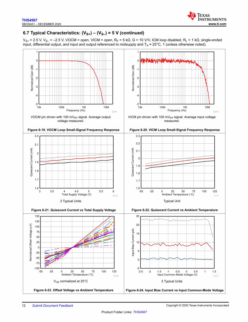
6.7 Typical Characteristics: (VS+) – (VS–) = 5 VVS+ = 2.5 V, VS– = –2.5 V, VOCM = open, VICM = open, RF = 5 kΩ, G = 10 V/V, ICM loop disabled, RL = 1 kΩ, single-endedinput, differential output, and input and output referenced to midsupply and TA ≈ 25°C, 1 (unless otherwise noted).
Frequency (Hz)
Norm
aliz
ed G
ain
(dB
)
-12
-9
-6
-3
0
3
1M 10M 100M
D201
G = 7 V/VG = 10 V/VG = 40 V/VG = 100 V/V
VOUT = 100 mVPP
Figure 6-1. Small-Signal Frequency Response vs Gain
Frequency (Hz)
Norm
aliz
ed G
ain
(dB
)
-12
-9
-6
-3
0
3
1M 10M 100M
D200
VOUT = 100 mVPP
VOUT = 1 VPP
VOUT = 5 VPP
VOUT = 8 VPP
Figure 6-2. Frequency Response vs VOUT
Frequency (Hz)
Norm
aliz
ed G
ain
(dB
)
-12
-9
-6
-3
0
3
1M 10M 100M
D205
CL = 10 pF, RISO = 0 :CL = 47 pF, RISO = 13 :CL = 100 pF, RISO = 13 :CL = 470 pF, RISO = 8 :CL = 1 nF, RISO = 5.6 :
Figure 6-3. Small-Signal Frequency Response vs CL
Frequency (Hz)
Norm
aliz
ed G
ain
(dB
)
-3
-2.5
-2
-1.5
-1
-0.5
0
0.5
1
1k 10k 100k 1M 10M
D206
VOUT = 8 VPP
Figure 6-4. Large-Signal Frequency Response Flatness
Frequency (Hz)
Voltage N
ois
e (
nV
/H
z)
1
10
100
1000
1k100 10k 100k 1M 10M100 1k 10k 100k 1M 10M
D207
Differential NoiseCommon-mode Noise
Figure 6-5. Input Referred Voltage Noise vs Frequency
Input Common-Mode Current (Each Input) (PA)
Cu
rre
nt
No
ise
(E
ach
In
pu
t) (
pA
/H
z)
0.1 1 10 1000.1
1
10
D220
f = 100 kHz, ICM loop enabled
Figure 6-6. Input Referred Current Noise vs ICM_CTL
www.ti.comTHS4567
SBOSA51 – DECEMBER 2020
Copyright © 2020 Texas Instruments Incorporated Submit Document Feedback 9
Product Folder Links: THS4567

6.7 Typical Characteristics: (VS+) – (VS–) = 5 V (continued)VS+ = 2.5 V, VS– = –2.5 V, VOCM = open, VICM = open, RF = 5 kΩ, G = 10 V/V, ICM loop disabled, RL = 1 kΩ, single-endedinput, differential output, and input and output referenced to midsupply and TA ≈ 25°C, 1 (unless otherwise noted).
Frequency (Hz)
Harm
onic
Dis
tort
ion (
dB
c)
-140
-130
-120
-110
-100
-90
-80
-70
-60
100 1k 10k 100k 1M
D208
HD2, VOUT = 2 VPP
HD3, VOUT = 2 VPP
HD2, VOUT = 8 VPP
HD3, VOUT = 8 VPP
Figure 6-7. Harmonic Distortion vs FrequencyOutput Voltage (VPP)
Harm
onic
Dis
tort
ion (
dB
c)
1 2 3 4 5 6 7 8 9-130
-120
-110
-100
-90
-80
-70
-60
-50
D209
HD2, 100 kHzHD3, 100 kHzHD2, 1 MHzHD3, 1 MHz
Figure 6-8. Harmonic Distortion vs VOUT
Load Resistance (:)
Ha
rmo
nic
Dis
tort
ion
(d
Bc)
-130
-120
-110
-100
-90
-80
-70
-60
-50
-40
-30
-20
100 1k 2k
D210
HD2, 100 kHz
HD3, 100 kHz
HD2, 1 MHz
HD3, 1 MHz
VOUT = 8 VPP
Figure 6-9. Harmonic Distortion vs RL
Output Common-Mode Voltage (V)
Ha
rmo
nic
Dis
tort
ion
(d
Bc)
-1.5 -1 -0.5 0 0.5 1 1.5-130
-120
-110
-100
-90
-80
-70
-60
-50
D211
HD2, 100 kHz
HD3, 100 kHzHD2, 1 MHz
HD3, 1 MHz
VOUT = 8 VPP
Figure 6-10. Harmonic Distortion vs VOCM
Frequency (Hz)
Harm
onic
Dis
tort
ion (
dB
c)
-120
-110
-100
-90
-80
-70
-60
-50
-40
-30
100k 1M 10M
D212
HD2, ICM_CTL = 5 PAHD3, ICM_CTL = 5 PAHD2, ICM_CTL = 25 PAHD3, ICM_CTL = 25 PAHD2, ICM_CTL = 100 PAHD3, ICM_CTL = 100 PA
VOUT = 8 VPP; Differential input to differential output; ICM LoopEnabled
Figure 6-11. Harmonic Distortion vs ICM_CTL
Center Frequency (MHz)
Dis
tort
ion (
dB
c)
1 10-90
-80
-70
-60
-50
-40
D224
IMD3IMD2
VOUT = 2 VPP (each tone), Tone separation from centerfrequency = 100 kHz
Figure 6-12. Intermodulation Distortion vs Frequency
THS4567SBOSA51 – DECEMBER 2020 www.ti.com
10 Submit Document Feedback Copyright © 2020 Texas Instruments Incorporated
Product Folder Links: THS4567

6.7 Typical Characteristics: (VS+) – (VS–) = 5 V (continued)VS+ = 2.5 V, VS– = –2.5 V, VOCM = open, VICM = open, RF = 5 kΩ, G = 10 V/V, ICM loop disabled, RL = 1 kΩ, single-endedinput, differential output, and input and output referenced to midsupply and TA ≈ 25°C, 1 (unless otherwise noted).
Time (100 ns/div.)
Voltage (
mV
)
-60
-40
-20
0
20
40
60
D213
InputOutput
tR/tF = 8 ns
Figure 6-13. Small-Signal Transient Response
Time (100 ns/div.)
Vo
lta
ge
(V
)
-5
-4
-3
-2
-1
0
1
2
3
4
5
D214
InputOutput
Slew rate (rising and falling) = 500 V/µs
Figure 6-14. Large-Signal Transient Response
Frequency (Hz)
Op
en
-Lo
op
Ga
in M
agn
itud
e (
dB
)
Op
en
-Lo
op
Ga
in P
ha
se
(q)
-40 -210
-20 -180
0 -150
20 -120
40 -90
60 -60
80 -30
100 0
120 30
1M 10M 100M100k10 10k100 1k
D223
AOL Magnitude (dB)AOL Phase (q)
Figure 6-15. Open-Loop Gain
Frequency (Hz)
Clo
sed-L
oop O
utp
ut Im
pedance (:
)
0.1
1
10
100
1M 10M100k10k
D215
G = 1 V/V, VOUT = 2 VPP, with VOCM adjusted
Figure 6-16. Closed-Loop Output Impedance vs Frequency
Frequency (Hz)
Pow
er
Supply
Reje
ction R
atio (
dB
)
40
50
60
70
80
90
100
110
120
1M 10M10 100k1 10k100 1k
D221
PSRR+PSRR-
Figure 6-17. Power-Supply Rejection Ratio vs Frequency
Frequency (Hz)
Com
mon-M
ode R
eje
ction R
atio (
dB
)
40
60
80
100
120
140
1M 10M 100M100k10k1k
D222
Figure 6-18. Common-Mode Rejection Ratio vs Frequency
www.ti.comTHS4567
SBOSA51 – DECEMBER 2020
Copyright © 2020 Texas Instruments Incorporated Submit Document Feedback 11
Product Folder Links: THS4567
6.7 Typical Characteristics: (VS+) – (VS–) = 5 V (continued)VS+ = 2.5 V, VS– = –2.5 V, VOCM = open, VICM = open, RF = 5 kΩ, G = 10 V/V, ICM loop disabled, RL = 1 kΩ, single-endedinput, differential output, and input and output referenced to midsupply and TA ≈ 25°C, 1 (unless otherwise noted).
Frequency (Hz)
No
rma
lize
d G
ain
(dB
)
-5
-4
-3
-2
-1
0
1
1M 10M100k10k
D218
VOCM pin driven with 100 mVPP signal. Average outputvoltage measured.
Figure 6-19. VOCM Loop Small-Signal Frequency Response
Frequency (Hz)
No
rma
lize
d G
ain
(dB
)
-5
-4
-3
-2
-1
0
1
1M 10M100k10k
D219
VICM pin driven with 100 mVPP signal. Average input voltagemeasured.
Figure 6-20. VICM Loop Small-Signal Frequency Response
Total Supply Voltage (V)
Quie
scent
Curr
ent
(mA
)
3 3.5 4 4.5 5 5.5 61.6
1.7
1.8
1.9
2
2.1
2.2
D170
3 Typical Units
Figure 6-21. Quiescent Current vs Total Supply Voltage
Ambient Temperature (qC)
Quie
scent
Curr
ent
(mA
)
-50 -25 0 25 50 75 100 1251.6
1.7
1.8
1.9
2
2.1
2.2
2.3
D171
Typical Unit
Figure 6-22. Quiescent Current vs Ambient Temperature
Ambient Temperature (qC)
Norm
aliz
ed O
ffset V
oltage (P
V)
-50 -25 0 25 50 75 100 125-100
-75
-50
-25
0
25
50
75
100
125
150
D102
VOS normalized at 25°C
Figure 6-23. Offset Voltage vs Ambient Temperature
Input Common-Mode Voltage (V)
Input
Bia
s C
urr
ent (p
A)
-2.5 -2 -1.5 -1 -0.5 0 0.5 1 1.5-5
0
5
10
15
20
25
D110
3 Typical Units
Figure 6-24. Input Bias Current vs Input Common-Mode Voltage
THS4567SBOSA51 – DECEMBER 2020 www.ti.com
12 Submit Document Feedback Copyright © 2020 Texas Instruments Incorporated
Product Folder Links: THS4567

6.7 Typical Characteristics: (VS+) – (VS–) = 5 V (continued)VS+ = 2.5 V, VS– = –2.5 V, VOCM = open, VICM = open, RF = 5 kΩ, G = 10 V/V, ICM loop disabled, RL = 1 kΩ, single-endedinput, differential output, and input and output referenced to midsupply and TA ≈ 25°C, 1 (unless otherwise noted).
Input Common-Mode Voltage (V)
Off
set V
oltage (
mV
)
-2.5 -2 -1.5 -1 -0.5 0 0.5 1 1.5-1.5
-1
-0.5
0
0.5
1
1.5
D103
3 Typical Units
Figure 6-25. Offset Voltage vs Input Common-Mode Voltage
Input Common-Mode Voltage (V)
Off
set V
oltage (
mV
)
-2.5 -2 -1.5 -1 -0.5 0 0.5 1 1.5-0.5
-0.25
0
0.25
0.5
D104
TA = 40qCTA = 25qCTA = 125qC
3 Typical Units
Figure 6-26. Offset Voltage vs Input Common-Mode Voltage vsAmbient Temperature
Differential Output Voltage (V)
Off
se
t V
olta
ge
(m
V)
-5 -4 -3 -2 -1 0 1 2 3 4 5-2
-1.5
-1
-0.5
0
0.5
1
1.5
2
D107
3 Typical Units, RL = 20 kΩ
Figure 6-27. Offset Voltage vs Differential Output Voltage
Differential Output Voltage (V)
Off
se
t V
olta
ge
(m
V)
-5 -4 -3 -2 -1 0 1 2 3 4 5-2
-1.5
-1
-0.5
0
0.5
1
1.5
2
D108
TA = -40qCTA = 25qCTA = 125qC
Typical Unit, RL = 20 kΩ
Figure 6-28. Offset Voltage vs Differential Output Voltage vsAmbient Temperature
Differential Output Voltage (V)
Off
se
t V
olta
ge
(m
V)
-5 -4 -3 -2 -1 0 1 2 3 4 5-2
-1.5
-1
-0.5
0
0.5
1
1.5
2
D111
3 Typical Units, RL = 1 kΩ
Figure 6-29. Offset Voltage vs Differential Output Voltage
Differential Output Voltage (V)
Off
se
t V
olta
ge
(m
V)
-5 -4 -3 -2 -1 0 1 2 3 4 5-2
-1.5
-1
-0.5
0
0.5
1
1.5
2
D112
TA = -40qCTA = 25qCTA = 125qC
Typical Unit, RL = 1 kΩ
Figure 6-30. Offset Voltage vs Differential Output Voltage vsAmbient Temperature
www.ti.comTHS4567
SBOSA51 – DECEMBER 2020
Copyright © 2020 Texas Instruments Incorporated Submit Document Feedback 13
Product Folder Links: THS4567

6.7 Typical Characteristics: (VS+) – (VS–) = 5 V (continued)VS+ = 2.5 V, VS– = –2.5 V, VOCM = open, VICM = open, RF = 5 kΩ, G = 10 V/V, ICM loop disabled, RL = 1 kΩ, single-endedinput, differential output, and input and output referenced to midsupply and TA ≈ 25°C, 1 (unless otherwise noted).
Differential Output Current (mA)
Diffe
rential O
utp
ut V
oltage (
V)
0 10 20 30 40 50
r5
r4.5
r4
r3.5
r3
r2.5
r2
r1.5
r1
r0.5
0
D120
3 Typical Units
Figure 6-31. Differential Output Voltage vs Load Current
Differential Output Current (mA)
Diffe
rential O
utp
ut V
oltage (
V)
0 10 20 30 40 50 60
r5
r4
r3
r2
r1
r4.5
r3.5
r2.5
r1.5
r0.5
0
D121
TA = 40qCTA = 25qCTA = 125qC
Typical Unit
Figure 6-32. Differential Output Voltage vs Load Current vsAmbient Temperature
Input Common-Mode Current, ICM_CTL (mA)
Avera
ge Input
Voltage, V
ICM
(V
)
-20 0 20 40 60 80 100-0.99
-0.96
-0.93
-0.9
-0.87
-0.84
-0.81
-0.78
-0.75
D125
VICM pin floating, 3 Typical Units
Figure 6-33. Average input Voltage vs Input Common-ModeCurrent
Input Common-Mode Current, ICM_CTL (mA)
Avera
ge Input
Voltage, V
ICM
(V
)
-20 0 20 40 60 80 100-0.96
-0.93
-0.9
-0.87
-0.84
-0.81
-0.78
-0.75
D126
TA = -40qCTA = 25qCTA = 125qC
VICM pin floating, Typical Unit
Figure 6-34. Average Input Voltage vs Input Common-ModeCurrent vs Ambient Temperature
VICM Set Voltage (V)
Avera
ge Input
Voltage, V
ICM
, (V
)
-2 -1.5 -1 -0.5 0 0.5 1 1.5-2
-1.5
-1
-0.5
0
0.5
1
1.5
2
D127
ICM_CTL = 5 PAICM_CTL = 20 PAICM_CTL = 50 PA
Typical Unit
Figure 6-35. Average Input Voltage vs VICM Set Voltage
VICM Set Voltage (V)
Avera
ge Input
Voltage, V
ICM
, (V
)
-2 -1.5 -1 -0.5 0 0.5 1 1.5-2
-1.5
-1
-0.5
0
0.5
1
1.5
2
D128
TA = -40qCTA = 25qCTA = 125qC
ICM_CTL = 20 µA, Typical Unit
Figure 6-36. Average Input Voltage vs VICM Set Voltage vsAmbient Temperature
THS4567SBOSA51 – DECEMBER 2020 www.ti.com
14 Submit Document Feedback Copyright © 2020 Texas Instruments Incorporated
Product Folder Links: THS4567

6.7 Typical Characteristics: (VS+) – (VS–) = 5 V (continued)VS+ = 2.5 V, VS– = –2.5 V, VOCM = open, VICM = open, RF = 5 kΩ, G = 10 V/V, ICM loop disabled, RL = 1 kΩ, single-endedinput, differential output, and input and output referenced to midsupply and TA ≈ 25°C, 1 (unless otherwise noted).
Output Common-Mode Voltage Set (V)
Ave
rag
e O
utp
ut
Vo
lta
ge
(m
V)
-2 -1.5 -1 -0.5 0 0.5 1 1.5 2-10
-8
-6
-4
-2
0
2
4
6
8
10
D115
VOCM offset = (VOCM - VOCM), 3 Typical Units
Figure 6-37. Output Common-Mode Offset Voltage vs OutputCommon-Mode Set Voltage
Ambient Temperature (qC)
Outp
ut
Com
mon-M
ode O
ffset
(V)
-50 -25 0 25 50 75 100 125-10
-8
-6
-4
-2
0
2
4
6
8
10
D116
VOCM = 0 V, 3 Typical Units
Figure 6-38. Output Common-Mode Offset Voltage vs AmbientTemperature
www.ti.comTHS4567
SBOSA51 – DECEMBER 2020
Copyright © 2020 Texas Instruments Incorporated Submit Document Feedback 15
Product Folder Links: THS4567

7 Detailed Description7.1 OverviewThe THS4567 device is a unique fully differential amplifier that features an input common-mode control loop inaddition to the output common-mode control loop typically found in all fully differential amplifiers. The THS4567device has a high impedance CMOS input stage with a very low input bias current. The independent input andoutput common-mode control along with the high impedance CMOS inputs make the THS4567 device an idealhigh-gain, low-noise, fully-differential transimpedance amplifier.
The input common-mode loop of the THS4567 device may be disabled by setting the ICM_EN pin below itsturnoff threshold voltage, turning it into a standard fully differential amplifier with output common-mode controlonly. The THS4567 device operates over a wide power supply voltage range from 3.3 V to 5.5 V, which makesthis device an excellent choice for driving differential ADCs and buffering DAC outputs.
This device features a low-power mode with a unique active pullup resistor that improves EMI reliability of theshutdown pin when left floating. The AMP_EN and ICM_EN pins draw very little bias current when the logicvoltage is outside the switching threshold region. Within the switching threshold region, the bias currentincreases, especially close to the transition region. The increased bias current prevents the logic frominadvertently switching in the presence of EMI.
7.2 Functional Block DiagramVS+
IN±
+
±
High-AOL
Differential I/OAmplifier
IN+
400 k
OUT+
OUT±
+
±
+
±
VOCMError
AmplifierVOCM
VS+
400 k
AMP_ENCMOS Buffer
VS±
VS±
Copyright © 2017, Texas Instruments Incorporated
6 k
+
±
VICMError
Amplifier
VICM
×1
×1
VS+
VS±
ICM_ENCMOS Buffer
6 k
181 k
8 A
THS4567SBOSA51 – DECEMBER 2020 www.ti.com
16 Submit Document Feedback Copyright © 2020 Texas Instruments Incorporated
Product Folder Links: THS4567

7.3 Feature DescriptionThe THS4567 architecture features three main building blocks:1. A high open loop gain differential I/O main amplifier.2. An output common-mode control error amplifier that sets the common-mode of the differential outputs of the
main amplifier.3. An input common-mode control error amplifier that sets the common-mode of the differential inputs of the
main amplifier, independent of the output common-mode.
7.3.1 Main Amplifier
The main differential I/O amplifier has a wide gain bandwidth product of 220 MHz and is stable in gainconfigurations > 10 V/V. Figure 6-15 shows the open-loop response of the main amplifier. The main amplifier hasa high-impedance CMOS input stage with very low input bias currents, which makes it ideal for use in high-gaintransimpedance systems or as a voltage amplifier with large feedback and gain resistors.
7.3.2 Output Common-Mode Control
The output common-mode loop works by sensing the average voltage between the two outputs of the mainamplifier through the two 6-kΩ resistors internal resistors in Section 7.2 and comparing it against the voltage atthe VOCM pin. The VOCM error amplifier then adjusts the internal bias of the main amplifier to minimize theerror voltage between its input pins. The voltage at the VOCM node defaults to midsupply through the two 400-kΩ internal bias string resistors between VS+ and VS–. When using the VOCM at its default voltage, connect anexternal capacitor to the VOCM pin to bypass the noise from the internal 400-kΩ resistors. When the amplifier isdisabled, the default midsupply bias string is disabled to save power. The THS4567 device output common-mode can also be set by driving the VOCM pin externally through a low output impedance source. Ensure thatthe source is capable of driving the input impedance of the VOCM pin.
7.3.3 Input Common-Mode Control
The THS4567 device features a unique input common-mode control error amplifier that sets the input common-mode voltage independent of the output common-mode voltage. The VICM error amplifier works by sensing theaverage voltage at the main amplifiers inputs and then sourcing or sinking an equal amount of current into boththe input nodes of the main amplifier to maintain the input common-mode voltage equal to voltage at the VICMpin. If the VICM pin is left floating, its input voltage defaults to 1.5-V above VS–. This voltage is set by thecombination of the 8-µA current source and the 181-kΩ resistor shown in Section 7.2. When using the VICM atits default voltage, connect an external capacitor to the VICM pin to bypass the noise from the internal 181-kΩresistor. The VICM voltage can be set to an arbitrary value by driving the VICM pin externally through a lowoutput impedance source. The input common-mode control loop can be disabled by setting ICM_EN pin low.With the input common-mode loop disabled the THS4567 device behaves like a standard fully-differentialamplifier (FDA).
www.ti.comTHS4567
SBOSA51 – DECEMBER 2020
Copyright © 2020 Texas Instruments Incorporated Submit Document Feedback 17
Product Folder Links: THS4567
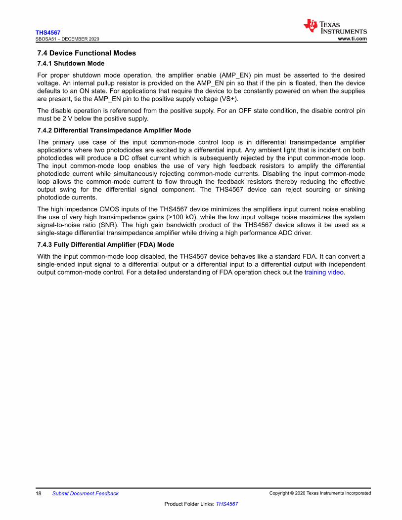
7.4 Device Functional Modes7.4.1 Shutdown Mode
For proper shutdown mode operation, the amplifier enable (AMP_EN) pin must be asserted to the desiredvoltage. An internal pullup resistor is provided on the AMP_EN pin so that if the pin is floated, then the devicedefaults to an ON state. For applications that require the device to be constantly powered on when the suppliesare present, tie the AMP_EN pin to the positive supply voltage (VS+).
The disable operation is referenced from the positive supply. For an OFF state condition, the disable control pinmust be 2 V below the positive supply.
7.4.2 Differential Transimpedance Amplifier Mode
The primary use case of the input common-mode control loop is in differential transimpedance amplifierapplications where two photodiodes are excited by a differential input. Any ambient light that is incident on bothphotodiodes will produce a DC offset current which is subsequently rejected by the input common-mode loop.The input common-mode loop enables the use of very high feedback resistors to amplify the differentialphotodiode current while simultaneously rejecting common-mode currents. Disabling the input common-modeloop allows the common-mode current to flow through the feedback resistors thereby reducing the effectiveoutput swing for the differential signal component. The THS4567 device can reject sourcing or sinkingphotodiode currents.
The high impedance CMOS inputs of the THS4567 device minimizes the amplifiers input current noise enablingthe use of very high transimpedance gains (>100 kΩ), while the low input voltage noise maximizes the systemsignal-to-noise ratio (SNR). The high gain bandwidth product of the THS4567 device allows it be used as asingle-stage differential transimpedance amplifier while driving a high performance ADC driver.
7.4.3 Fully Differential Amplifier (FDA) Mode
With the input common-mode loop disabled, the THS4567 device behaves like a standard FDA. It can convert asingle-ended input signal to a differential output or a differential input to a differential output with independentoutput common-mode control. For a detailed understanding of FDA operation check out the training video.
THS4567SBOSA51 – DECEMBER 2020 www.ti.com
18 Submit Document Feedback Copyright © 2020 Texas Instruments Incorporated
Product Folder Links: THS4567
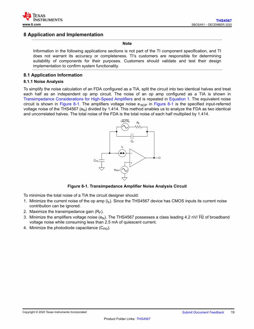
8 Application and ImplementationNote
Information in the following applications sections is not part of the TI component specification, and TIdoes not warrant its accuracy or completeness. TI’s customers are responsible for determiningsuitability of components for their purposes. Customers should validate and test their designimplementation to confirm system functionality.
8.1 Application Information8.1.1 Noise Analysis
To simplify the noise calculation of an FDA configured as a TIA, split the circuit into two identical halves and treateach half as an independent op amp circuit. The noise of an op amp configured as a TIA is shown inTransimpedance Considerations for High-Speed Amplifiers and is repeated in Equation 1. The equivalent noisecircuit is shown in Figure 8-1. The amplifiers voltage noise e NOP in Figure 8-1 is the specified input-referredvoltage noise of the THS4567 (eN) divided by 1.414. This method enables us to analyze the FDA as two identicaland uncorrelated halves. The total noise of the FDA is the total noise of each half multiplied by 1.414.
CPD
eNOP
ib
+
±
RF
CF
¥4kTRF
Figure 8-1. Transimpedance Amplifier Noise Analysis Circuit
To minimize the total noise of a TIA the circuit designer should:1. Minimize the current noise of the op amp (ib). Since the THS4567 device has CMOS inputs its current noise
contribution can be ignored.2. Maximize the transimpedance gain (RF).3. Minimize the amplifiers voltage noise (eN). The THS4567 possesses a class leading 4.2 nV/ Hz of broadband
voltage noise while consuming less than 2.5 mA of quiescent current.4. Minimize the photodiode capacitance (CPD).
www.ti.comTHS4567
SBOSA51 – DECEMBER 2020
Copyright © 2020 Texas Instruments Incorporated Submit Document Feedback 19
Product Folder Links: THS4567

The capacitance of a photodiode can be minimized by increasing its reverse bias. The THS4567 input andoutput common-mode can be independently controlled. The independent control feature allows the circuitdesigner to set photodiode's anode close to the negative supply voltage while tying its cathode close to thepositive supply voltage to maximize the reverse bias across the photodiode. The output common-mode is thenset to match the next stage ADCs input common-mode range. In a standard op amp TIA, the input common-mode is biased close to the positive supply to maximize the output swing of the amplifier. This bias configurationlimits the reverse bias across the photodiode thereby increasing its input capacitance. The THS4567 device isoptimized to reduce total system noise by optimizing the noise source from each contributing source in Equation1.
2/
3
242
2
2
»»¼
º
««¬
ª ¸
¹
ᬩ
§ sn
F
n
F
bEQ
CFe
R
e
R
kTii
S
(1)
where
• ib = current noise of the THS4567 device• 4kT = 16 × 10–21J at 290 degrees Kelvin• RF = feedback resistor• eN = voltage noise of the THS4567 device• CS = total input capacitance from the THS4567, photodiode and any PCB parasitics• F = noise integration frequency limit
8.2 Typical ApplicationThe primary use case for the THS4567 input common-mode loop is in differential transimpedance applicationsthat have a large common-mode offset due to ambient light. In this section we compare the performance of theTHS4567 device with the input common-mode loop enabled (TIA mode) as shown in Figure 8-2 versus adifferential TIA implementation built using two discrete op amp channels (OPA mode) as shown in Figure 8-3.
VBIAS
IPD+
IPD–
VICM = 1 V
+
–
+
–
5.25 V
–0.25 V
RFILT
RFILT’
10-VPP Differential SAR
ADC InputCFILTVOCM = 2.5 V
VBIAS
RF'
CF'
RF
CF
Figure 8-2. THS4567 with Integrated Differential TIA + ADC Driver
THS4567SBOSA51 – DECEMBER 2020 www.ti.com
20 Submit Document Feedback Copyright © 2020 Texas Instruments Incorporated
Product Folder Links: THS4567

VOCM = 2.5 V
RFILT
RFILT’
10-VPP Differential SAR
ADC InputCFILT
+
–
+
–
5.25 V
–0.25 V
–0.25 V
5.25 V
RF
CF
VBIAS
IPD+
5 V
RF'
CF'
IPD–
+
–
+
–THS4561
5.25 V
–0.25 V
R1
R1'
R2
R2'VBIAS
Figure 8-3. Discrete Differential Op Amp TIA + 2nd Stage ADC Driver
8.2.1 Design Requirements
The requirements for this application are:
• Supply voltage: 5.5 V• ADC full-scale range: 10 VPP differential• ADC input common-mode voltage: 2.5 V• Ambient light current offset (DC): 10 µA• Single-sided signal current: 5 µAPP (each photodiode). Differential signal current = 10 µAPP• Input signal frequency: 100 kHz
www.ti.comTHS4567
SBOSA51 – DECEMBER 2020
Copyright © 2020 Texas Instruments Incorporated Submit Document Feedback 21
Product Folder Links: THS4567

8.2.2 Detailed Design Procedure (THS4567 in TIA Mode)
The output current from each photodiode is shown in Figure 8-4. A detailed procedure on how to set the variousbias voltages and select the optimal value of transimpedance gain follows.
• Set VS+ = 5.25 V and VS– = –0.25 V to allow the THS4567 to swing 10 VPP (differential) without introducingdistortion due to limited headroom.
• Set ICM_EN = logic high to enable the THS4567 TIA mode of operation.• Set VOCM to 2.5 V to match the ADC input common-mode range.• With the photodiodes (PDs) configured with a cathode bias as shown in Figure 8-2 both PDs will source
current when light is incident on them. To maximize the reverse bias across the PD, VBIAS is typically set tothe amplifiers positive supply voltage or the highest available positive supply voltage.
• The maximum output current from the PD is the sum of the ambient light current and the maximum signalcurrent.
ITOTAL = IAMBIENT + ISIGNAL = 10 µA + 5 µA = 15 µA (2)
• In the TIA mode, VICM is set to its minimum input common-mode compliance limit (1.25 V) to maximize thereverse bias across the PDs thereby reducing the PD capacitance.
Reverse bias across the photodiodes = (5.25 V - 1.25 V) = 4 V (3)
• In the TIA mode, the ICM loop cancels the common-mode input current due to ambient light (10 µA) at theamplifier's input pin and only the differential signal current flows through the feedback resistors RF and RF'.The maximum TIA gain is therefore the ratio of the maximum differential output swing and the maximumdifferential signal current as shown in Equation 4.
Maximum TIA gain = (10 VPP/ 10 µA) = 1 MΩ (4)
• Once the feedback resistor value is set, select the value of feedback capacitance as described inTransimpedance Considerations for High-Speed Amplifiers.
Time (Ps)
Photo
dio
de o
utp
ut curr
ent (P
A)
0 2.5 5 7.5 10 12.5 15 17.5 200
2.5
5
7.5
10
12.5
15
17.5
20IPD+
IPD-
Signal
Current
Ambient
Light
Figure 8-4. Photodiode Differential Output Current
THS4567SBOSA51 – DECEMBER 2020 www.ti.com
22 Submit Document Feedback Copyright © 2020 Texas Instruments Incorporated
Product Folder Links: THS4567

8.2.2.1 OPA Mode Configuration
The OPA mode configuration is shown in Figure 8-3. This configuration results in a reverse bias of (5.25 V - 5 V= 0.25 V) across the PD thereby greatly increasing the PD capacitance compared to the TIA mode.
In the OPA mode there is no input common-mode current cancellation so the maximum value of feedbackresistance (RF, RF') is the ratio of the maximum single-ended output swing and the maximum single-ended inputcurrent as shown in Equation 5.
Maximum TIA gain = (5 V/15 µA) = 333.33 kΩ (5)
The total differential swing is 333.33 kΩ × 10 µAPP = 3.33 V. To maximize the ADC gain range a subsequentamplifier gain stage is needed. The second gain stage which is typically implemented with a standard FDA likethe THS4561 will also adjust the output common-mode to match the ADCs input common-mode compliancerange.
As the level of ambient light increases relative to the differential signal from the PD, the maximum gainconfiguration in the OPA mode will decrease while it stays constant for the THS4567 TIA mode.
8.2.3 Application Curves
Figure 8-5 shows the output of the THS4567 device in TIA mode. The output common-mode is centered onVOCM = 2.5 V and the differential output of 10 V PP maximizes the subsequent ADCs entire common-moderange.
Figure 8-6 shows the output of the first stage transimpedance amplifier setup shown in Figure 8-3. The outputcommon-mode is centered on 0.83 V. The offset in the common-mode is caused by the offset due to the ambientlight. More importantly the differential output swing is only 3.33 V. To maximize the ADC dynamic range thesubsequent THS4561 differential amplifier stage is configured in a signal gain of 3 V/V. The THS4561 device willalso perform a level shift to center the output common-mode to 2.5 V.
Time (Ps)
Outp
ut V
oltage (
V)
0 2.5 5 7.5 10 12.5 15 17.5 20-2.5
0
2.5
5
7.5
D500
VOUT-
VOUT+
Figure 8-5. Output of THS4567 (TIA Mode)Time (Ps)
Opam
p S
tage O
utp
ut V
oltage
(V
)
0 2.5 5 7.5 10 12.5 15 17.5 20-1.5
0
1.5
3
4.5VOUT-
VOUT+
Figure 8-6. Output of the 1st Stage Discrete OpAmp Transimpedance Amplifier (OPA Mode)
The noise performance of the THS4567 device (half-circuit) is then compared against the noise of the OPA607and the OPA365 in OPA mode. Using Equation 1 we can estimate the total input referred spot noise for theTHS4567 device. Transimpedance Considerations for High-Speed Amplifiers is used to estimate the noise of theOPA607 and OPA365 transimpedance amplifier stage in OPA mode.
www.ti.comTHS4567
SBOSA51 – DECEMBER 2020
Copyright © 2020 Texas Instruments Incorporated Submit Document Feedback 23
Product Folder Links: THS4567

A PD capacitance of 5 pF is assumed. In a real world system the PD capacitance will be higher in OPA modebecause of the lower reverse bias across the PD. The calculated noise results are shown in Table 8-1 where thebenefit of the THS4567 device can clearly be seen. The spot noise has been normalized to the closed loopbandwidth. The OPA mode architecture would require a second gain stage to maximize the ADCs input full scalerange. The second stage would increase the power consumption and degrade the noise.
Table 8-1. Noise ComparisonAmplifier Specification THS4567 OPA607 OPA365
Photodiode Capacitance (pF) 5 5 5
Amplifier Input Capacitance (pF) 1 17 8
Amplifier Voltage Noise (nV/√ Hz) 4.2 3.8 4.5
TIA Gain (kΩ) 1000 333.33 333.33
Closed Loop Bandwidth (MHz) 2.4 1 1.4
Input-Referred Spot Noise (pA/√ Hz) 0.2 0.39 0.36
8.3 Differential TIA with 0-V Biased PhotodiodeThe circuit in Figure 8-7 can be used for a differential TIA with 0-V reverse bias across the photodiode. TheVICM loop should be disabled in this configuration since the loop can only source or sink DC current. Any DCcurrent generated by the photodiode in the configuration shown will be differential in nature.
IPD+
IPD–
VICM
(disabled)
+
–
+
–
VS+
VS–
VOCM = 2.5 V
RF'
CF'
RF
CF
Figure 8-7. Differential TIA with 0-V Biased Photodiode
THS4567SBOSA51 – DECEMBER 2020 www.ti.com
24 Submit Document Feedback Copyright © 2020 Texas Instruments Incorporated
Product Folder Links: THS4567

8.4 Differential AC Coupled TIAThe circuit in Figure 8-8 can be used as a differential AC-coupled TIA with variable reverse bias across thephotodiode. Since no DC current flows in the feedback network due to the AC coupling the VICM loop can bedisabled.
IPD+
IPD–
VICM
(disabled)
+
–
+
–
VS+
VS–
VOCM = 2.5 V
RF'
CF'
RF
CF
+VBIAS
–VBIAS
Figure 8-8. Differential AC Coupled TIA
9 Power Supply RecommendationsThe THS4567 device is principally intended to operate with a nominal single-supply voltage of 3.3 V to 5.5 V.Split (or bipolar) supplies can be used with the THS4567 device, as long as the total value across the deviceremains less than 5.5 V. A low power-supply source impedance must be maintained across frequency so usemultiple bypass capacitors in parallel. Place the bypass capacitors as close to the supply pins as possible. Placethe smallest capacitor (< 10 nF) on the same side of the PCB as the THS4567 device. Larger capacitors (> 1 µF)can be placed further away and shared among different devices in the system.
www.ti.comTHS4567
SBOSA51 – DECEMBER 2020
Copyright © 2020 Texas Instruments Incorporated Submit Document Feedback 25
Product Folder Links: THS4567

10 Layout10.1 Layout Guidelines10.1.1 Board Layout Recommendations
Similar to all high-speed devices, best system performance is achieved with close attention to board layout.General high-speed signal path layout suggestions include:
• Continuous ground planes are preferred for signal routing with matched impedance traces for longer runs;however, both ground and power planes must be opened up around the capacitive sensitive input and outputdevice pins. When the signal goes to a resistor, parasitic capacitance becomes more of a band-limiting issueand less of a stability issue.
• Good high-frequency decoupling capacitors (0.01 µF) are required to a ground plane at the device powerpins. Additional higher-value capacitors (2.2 µF) are also required but can be placed further from the devicepower pins and shared among devices. For best high-frequency decoupling, consider X2Y supply decouplingcapacitors that offer a much higher self-resonance frequency over standard capacitors.
• Differential signal routing over any appreciable distance must use microstrip layout techniques with matchedimpedance traces.
• The THS4567 outputs are sensitive to capacitive loading. Isolate the output of the THS4567 from anycapacitive load by placing series isolation resistors close to the amplifiers output pins.
10.2 Layout Example
OUT–
ICM_EN VICM
AMP_EN VOCM
IN+ IN-
VS–
VS+
+
+
¯
¯
GND
GND
VS+
OUT+
VS+
Place bypass capacitors close to VDD
and GND pins on the same side as
DUT. Use multiple vias to connect to
power and GND planes
Place feedback elements
close to DUT
Series isolation resistors on each
differential output to isolate device
outputs from PCB capacitance
Place photodiodes close to device inputs
to minimize parasitic capacitance
Optional noise bypass capacitors on
VICM and VOCM inputs. Capacitors
placed on bottom of PCB through vias
Figure 10-1. Example Layout
THS4567SBOSA51 – DECEMBER 2020 www.ti.com
26 Submit Document Feedback Copyright © 2020 Texas Instruments Incorporated
Product Folder Links: THS4567
11 Device and Documentation Support11.1 Documentation Support11.1.1 Related Documentation
For related documentation see the following:• Texas Instruments,RUN_FDA_4567 EVM user's guide• Texas Instruments, Fully-Differential Amplifiers application note• Texas Instruments, Fully Differential Amplifiers TI Precision Labs
11.2 Receiving Notification of Documentation UpdatesTo receive notification of documentation updates, navigate to the device product folder on ti.com. In the upperright corner, click on Alert me to register and receive a weekly digest of any product information that haschanged. For change details, review the revision history included in any revised document.
11.3 Support ResourcesTI E2E™ support forums are an engineer's go-to source for fast, verified answers and design help — straightfrom the experts. Search existing answers or ask your own question to get the quick design help you need.
Linked content is provided "AS IS" by the respective contributors. They do not constitute TI specifications and donot necessarily reflect TI's views; see TI's Terms of Use.
11.4 TrademarksTI E2E™ is a trademark of Texas Instruments.All trademarks are the property of their respective owners.11.5 Electrostatic Discharge Caution
This integrated circuit can be damaged by ESD. Texas Instruments recommends that all integrated circuits be handledwith appropriate precautions. Failure to observe proper handling and installation procedures can cause damage.ESD damage can range from subtle performance degradation to complete device failure. Precision integrated circuits maybe more susceptible to damage because very small parametric changes could cause the device not to meet its publishedspecifications.
11.6 GlossaryTI Glossary This glossary lists and explains terms, acronyms, and definitions.
12 Mechanical, Packaging, and Orderable InformationThe following pages include mechanical, packaging, and orderable information. This information is the mostcurrent data available for the designated devices. This data is subject to change without notice and revision ofthis document. For browser-based versions of this data sheet, refer to the left-hand navigation.
www.ti.comTHS4567
SBOSA51 – DECEMBER 2020
Copyright © 2020 Texas Instruments Incorporated Submit Document Feedback 27
Product Folder Links: THS4567

PACKAGE OPTION ADDENDUM
www.ti.com 23-Feb-2021
Addendum-Page 1
PACKAGING INFORMATION
Orderable Device Status(1)
Package Type PackageDrawing
Pins PackageQty
Eco Plan(2)
Lead finish/Ball material
(6)
MSL Peak Temp(3)
Op Temp (°C) Device Marking(4/5)
Samples
THS4567IRUNR ACTIVE QFN RUN 10 3000 RoHS & Green NIPDAU Level-2-260C-1 YEAR -40 to 125 SN67
(1) The marketing status values are defined as follows:ACTIVE: Product device recommended for new designs.LIFEBUY: TI has announced that the device will be discontinued, and a lifetime-buy period is in effect.NRND: Not recommended for new designs. Device is in production to support existing customers, but TI does not recommend using this part in a new design.PREVIEW: Device has been announced but is not in production. Samples may or may not be available.OBSOLETE: TI has discontinued the production of the device.
(2) RoHS: TI defines "RoHS" to mean semiconductor products that are compliant with the current EU RoHS requirements for all 10 RoHS substances, including the requirement that RoHS substancedo not exceed 0.1% by weight in homogeneous materials. Where designed to be soldered at high temperatures, "RoHS" products are suitable for use in specified lead-free processes. TI mayreference these types of products as "Pb-Free".RoHS Exempt: TI defines "RoHS Exempt" to mean products that contain lead but are compliant with EU RoHS pursuant to a specific EU RoHS exemption.Green: TI defines "Green" to mean the content of Chlorine (Cl) and Bromine (Br) based flame retardants meet JS709B low halogen requirements of <=1000ppm threshold. Antimony trioxide basedflame retardants must also meet the <=1000ppm threshold requirement.
(3) MSL, Peak Temp. - The Moisture Sensitivity Level rating according to the JEDEC industry standard classifications, and peak solder temperature.
(4) There may be additional marking, which relates to the logo, the lot trace code information, or the environmental category on the device.
(5) Multiple Device Markings will be inside parentheses. Only one Device Marking contained in parentheses and separated by a "~" will appear on a device. If a line is indented then it is a continuationof the previous line and the two combined represent the entire Device Marking for that device.
(6) Lead finish/Ball material - Orderable Devices may have multiple material finish options. Finish options are separated by a vertical ruled line. Lead finish/Ball material values may wrap to twolines if the finish value exceeds the maximum column width.
Important Information and Disclaimer:The information provided on this page represents TI's knowledge and belief as of the date that it is provided. TI bases its knowledge and belief on informationprovided by third parties, and makes no representation or warranty as to the accuracy of such information. Efforts are underway to better integrate information from third parties. TI has taken andcontinues to take reasonable steps to provide representative and accurate information but may not have conducted destructive testing or chemical analysis on incoming materials and chemicals.TI and TI suppliers consider certain information to be proprietary, and thus CAS numbers and other limited information may not be available for release.
In no event shall TI's liability arising out of such information exceed the total purchase price of the TI part(s) at issue in this document sold by TI to Customer on an annual basis.

www.ti.com
PACKAGE OUTLINE
2.11.9
2.11.9
0.80.7
0.050.00
2X 1.5
6X 0.5
10X 0.60.4
10X 0.30.2
(0.2) TYP
WQFN - 0.8 mm max heightRUN0010APLASTIC QUAD FLATPACK - NO LEAD
4220470/A 05/2020
0.08 C
0.1 C A B0.05
NOTES: 1. All linear dimensions are in millimeters. Any dimensions in parenthesis are for reference only. Dimensioning and tolerancing per ASME Y14.5M. 2. This drawing is subject to change without notice.
PIN 1 INDEX AREA
SEATING PLANE
PIN 1 ID
SYMM
SYMM
1
45
6
9
10
SCALE 5.000
AB
C

www.ti.com
EXAMPLE BOARD LAYOUT
6X (0.5)
(R0.05) TYP
0.07 MAXALL AROUND
0.07 MINALL AROUND
10X (0.7)
10X (0.25)
(1.7)
(1.7)
WQFN - 0.8 mm max heightRUN0010APLASTIC QUAD FLATPACK - NO LEAD
4220470/A 05/2020
NOTES: (continued) 3. This package is designed to be soldered to a thermal pad on the board. For more information, see Texas Instruments literature number SLUA271 (www.ti.com/lit/slua271).
SYMM
SYMM
LAND PATTERN EXAMPLEEXPOSED METAL SHOWN
SCALE: 20X
SEE SOLDER MASKDETAIL
1
4
5
6
9
10
METAL EDGE
SOLDER MASKOPENING
EXPOSED METAL
METAL UNDERSOLDER MASK
SOLDER MASKOPENING
EXPOSEDMETAL
NON SOLDER MASKDEFINED
(PREFERRED)SOLDER MASK DEFINED
SOLDER MASK DETAILS

www.ti.com
EXAMPLE STENCIL DESIGN
10X (0.7)
10X (0.25)
6X (0.5)
(1.7)
(1.7)
(R0.05) TYP
WQFN - 0.8 mm max heightRUN0010APLASTIC QUAD FLATPACK - NO LEAD
4220470/A 05/2020
NOTES: (continued) 4. Laser cutting apertures with trapezoidal walls and rounded corners may offer better paste release. IPC-7525 may have alternate design recommendations.
SOLDER PASTE EXAMPLEBASED ON 0.125 MM THICK STENCIL
SCALE: 20X
SYMM
SYMM
1
4
5
6
9
10

IMPORTANT NOTICE AND DISCLAIMERTI PROVIDES TECHNICAL AND RELIABILITY DATA (INCLUDING DATASHEETS), DESIGN RESOURCES (INCLUDING REFERENCEDESIGNS), APPLICATION OR OTHER DESIGN ADVICE, WEB TOOLS, SAFETY INFORMATION, AND OTHER RESOURCES “AS IS”AND WITH ALL FAULTS, AND DISCLAIMS ALL WARRANTIES, EXPRESS AND IMPLIED, INCLUDING WITHOUT LIMITATION ANYIMPLIED WARRANTIES OF MERCHANTABILITY, FITNESS FOR A PARTICULAR PURPOSE OR NON-INFRINGEMENT OF THIRDPARTY INTELLECTUAL PROPERTY RIGHTS.These resources are intended for skilled developers designing with TI products. You are solely responsible for (1) selecting the appropriateTI products for your application, (2) designing, validating and testing your application, and (3) ensuring your application meets applicablestandards, and any other safety, security, or other requirements. These resources are subject to change without notice. TI grants youpermission to use these resources only for development of an application that uses the TI products described in the resource. Otherreproduction and display of these resources is prohibited. No license is granted to any other TI intellectual property right or to any third partyintellectual property right. TI disclaims responsibility for, and you will fully indemnify TI and its representatives against, any claims, damages,costs, losses, and liabilities arising out of your use of these resources.TI’s products are provided subject to TI’s Terms of Sale (https:www.ti.com/legal/termsofsale.html) or other applicable terms available eitheron ti.com or provided in conjunction with such TI products. TI’s provision of these resources does not expand or otherwise alter TI’sapplicable warranties or warranty disclaimers for TI products.IMPORTANT NOTICE
Mailing Address: Texas Instruments, Post Office Box 655303, Dallas, Texas 75265Copyright © 2021, Texas Instruments Incorporated