i.mx 6 series ddr calibration - nxp...
TRANSCRIPT
Freescale SemiconductorApplication Note
© 2015 Freescale Semiconductor, Inc. All rights reserved.
1 IntroductionThe purpose of this document is to describe how to perform various calibration processes on the i.MX 6 Series Multi Mode DDR Controller (MMDC) for use with DDR3 and LPDDR2 memories. These calibration processes are needed to fine tune various delay-line parameters in MMDC for optimal performance and functionality at the target frequency selected by the user.
NOTEUnless otherwise noted, content provided in this document applies to all i.MX 6 Series products: Quad, Dual, DualLite, Solo, SoloLite, and SoloX.
Contents1. Introduction . . . . . . . . . . . . . . . . . . . . . . . . . . . . . . . . . 12. DDR Calibration Modes . . . . . . . . . . . . . . . . . . . . . . . 23. Using Calibration for Different DDR Standards . . . . 34. Calibration over Frequency Range . . . . . . . . . . . . . . . 55. Calibration and Chip Selects . . . . . . . . . . . . . . . . . . . . 66. Source of Calibration Delay Values . . . . . . . . . . . . . . 67. Using DDR Calibration Modes . . . . . . . . . . . . . . . . . . 68. Delay Unit Hardware Overview . . . . . . . . . . . . . . . . . 99. Address and Data Content Used for
Timing Calibration . . . . . . . . . . . . . . . . . . . . . . . . . . 1010. ZQ Calibration . . . . . . . . . . . . . . . . . . . . . . . . . . . . . 1111. Write Leveling . . . . . . . . . . . . . . . . . . . . . . . . . . . . . 1612. DQS Gating . . . . . . . . . . . . . . . . . . . . . . . . . . . . . . . . 2113. Read DQS Delay Calibration . . . . . . . . . . . . . . . . . . 2614. Write DQS Delay Calibration . . . . . . . . . . . . . . . . . . 2915. Read Data Bit Delay Calibration . . . . . . . . . . . . . . . 3116. Write Data Bit Delay Calibration . . . . . . . . . . . . . . . 3217. Clock Delay Calibration . . . . . . . . . . . . . . . . . . . . . . 3218. CA-Bus Bit Delay Calibration . . . . . . . . . . . . . . . . . 3219. DDR Calibration Code Examples . . . . . . . . . . . . . . . 3320. Reference Documents . . . . . . . . . . . . . . . . . . . . . . . . 4821. Revision History . . . . . . . . . . . . . . . . . . . . . . . . . . . . 49
i.MX 6 Series DDR Calibrationby Freescale Semiconductor, Inc.
Document Number: AN4467Rev. 2, 03/2015
i.MX 6 Series DDR Calibration, Rev. 2
2 Freescale Semiconductor
DDR Calibration Modes
2 DDR Calibration ModesThe i.MX 6 Series DDR interface supports following nine calibration parameter settings:
• ZQ calibration: Changes the values of the on-chip pull-up and pull-down resistors connected to the VCC/2 pins. Unlike all other types of calibration that take place only at the i.MX 6 Series DDR port, ZQ calibration takes place in the DDR device side as well.
• Write leveling calibration: In DDR3 mode, set DQS, DQ, and DM signals of each data byte to their common timing delay relative to DDR CLK, ADDR, and Controls. This calibration is associated with the DDR3 “fly-by” board topology, as described by the JESD79-3E standard. These settings are not used in LPDDR2 mode.
• DQS gating calibration: Optimize the timing of MMDC mask of the incoming DQS signal during read access.
• Read data DQS calibration: Set DQS input of each data byte to its delay relative to the byte DQ inputs.
• Write data DQS calibration: Set DQS output of each data byte to its delay relative to the byte DQ and DM outputs.
• Read data bit delay calibration: Additional delay for each input data bit.
• Write data bit delay calibration: Additional delay for each output data bit.
• Clock signal delay calibration: Additional delay for the SDCLK and SDCLK_B signals.
• CA-bus bit delay calibration: In LPDDR2 mode, additional delay is available for each bit of the command/address CA-bus.
i.MX 6 Series DDR Calibration, Rev. 2
Freescale Semiconductor 3
Using Calibration for Different DDR Standards
3 Using Calibration for Different DDR Standards
3.1 DDR3All the above calibration processes except CA-bus bit delay calibration can be used for DDR3 calibration. The i.MX 6Dual/6Quad and i.MX 6Solo/6DualLite support two DDR3 modes: single channel 32-bits and single channel 64-bits. The i.MX 6SoloLite and i.MX 6SoloX only support single channel 32-bits DDR3 mode. The i.MX 6SoloX only supports single channel 32-bits DDR3 mode.
For 32-bits operation, only MMDC0 registers are used for calibration and delay lines setup, as shown in Figure 1.
Figure 1. DDR3 32-Bit Calibration Registers
MMDC0
DDR Logic 0
DDR Control Regs
MMDC1
DDR Logic 1
DDR ControlRegs
channel #1, 32-bits
DDR PHY 0
CalibrationControl
DDR PHY 1
CalibrationStatus
Delay Regs
CalibrationControl
CalibrationStatus
Delay Regs
frc_msr
frc_msr
i.MX 6 Series DDR Calibration, Rev. 2
4 Freescale Semiconductor
Using Calibration for Different DDR Standards
For 64-bits operation, DDR control registers are active for MMDC0 only. Calibration control bits (calibration enable and other calibration configurations) are also active for DDR PHY0 only. Delay value, status (error bits, abs delay units) registers and frc_msr bit, on the other hand, are active for both MMDC0 and MMDC1, as shown in Figure 2. In 64-bits mode, DDR and calibration logic of MMDC0 is designed to take over the DDR PHY of MMDC1, and perform the calibration sequence for the entire 64-bits. DDR_PHY0 delay and status registers are used for calibration of DQ[31:0] and associated DQS, DQM signals (as well as DDR clock). DDR_PHY1 delay and status registers are used for calibration of DQ[63:32] and associated DQS, DQM signals.
Figure 2. DDR3 64-Bit Calibration Registers
MMDC0
DDR Logic 0 DDR PHY 0
CalibrationControl
DDR Control Regs
MMDC1
DDR Logic 1 DDR PHY 1
DDR Control Regs
channel #1, 64-bits
CalibrationStatus
Delay Regs
CalibrationControl
CalibrationStatus
Delay Regs
frc_msr
frc_msr
i.MX 6 Series DDR Calibration, Rev. 2
Freescale Semiconductor 5
Calibration over Frequency Range
3.2 LPDDR2All the above calibration processes except DQS gating calibration and write leveling calibration can be used for LPDDR2 calibration.
The i.MX 6Dual/6Quad and i.MX 6Solo/6DualLite support both single and dual 32-bits LPDDR2 modes. The i.MX 6SoloLite and i.MX 6SoloX only support single channel 32-bits LPDDR2 mode.
For single channel, only MMDC0 registers are used for calibration and delay lines setup. It uses a setup similar to the DDR3 setup shown in Figure 1.
For dual channel operation, calibration and delay setup are done separately, for channel #1 by MMDC0 and for channel #2 by MMDC1, as shown in Figure 3.
Figure 3. LPDDR2 Dual Channel Calibration Registers
4 Calibration over Frequency RangeCalibration, as any other aspect of the DDR setup, is frequency dependant. Changing DDR clock frequency requires running the various calibration sequences and obtaining new set of delay values.
The empirical rule is that a DDR setup for a target frequency, including a measured set of delay values at that frequency, is expected to be stable at frequency range of ±10% around this point.
MMDC0
DDR Logic 0
DDR Control Regs
MMDC1
DDR Logic 1
DDR Control Regs
channel #1, 32-bits
channel #2, 32-bits
DDR PHY 0
CalibrationControl
CalibrationStatus
Delay Regs frc_msr
DDR PHY 1
CalibrationControl
CalibrationStatus
Delay Regs frc_msr
i.MX 6 Series DDR Calibration, Rev. 2
6 Freescale Semiconductor
Calibration and Chip Selects
5 Calibration and Chip Selects The user has the option of populating DDR memory devices on chip select 0 (CSD0), chip select 1 (CSD1), or both chip selects. The control mechanism to decide which chip select the associated calibration is targeted to is found in MDMISC[CALIB_PER_CS] bit. If the DDR memory devices are populated on CSD0, then this bit would be cleared. If these devices are populated only on CSD1, then this bit would be set. Should both chip selects be populated, it is an absolute must that the memories populated on CSD1 are “mirrored” with the memories populated on CSD0, as both CSD share the same delay line register set during normal DDR operation. Given the similarities in memory device layout, either setting can be used for MDMISC[CALIB_PER_CS] bit. However, the examples in this document clear this bit, hence targeting calibration toward CSD0.
NOTEThe i.MX 6Dual/Quad and the i.MX 6Solo/DualLite have two different SDCLK signals. It is important to note that the term "mirrored" also means that the same SDCLK[0 or 1] trace be routed to both CSD0 and CSD1 chips of the same byte lane. If different SDCLK traces are proved to CSD0 and CSD1 devices, differences between the two clock traces may result in slight timing errors.
6 Source of Calibration Delay ValuesEach of the calibration processes of Section 2, “DDR Calibration Modes” is supported by register(s) in MMDC that hold its delay values. Source of delay values might be:
• Analysis of board features and layout
• Trial and error run of different delay values, using a selected DDR test pattern
• Iterative calibration sequence to select best delay values, based on MMDC logic
While first two methods are supported for all calibration processes, the iterative calibration sequence is only provided for:
• ZQ calibration
• Write leveling calibration
• DQS gating calibration
• Read data DQS calibration
• Write data DQS calibration
7 Using DDR Calibration Modes
7.1 Calibration Usage General NotesCalibration sequence should be executed after the DDR memory has been initialized.
Calibration sequence should be executed by code mounted on the internal RAM of the i.MX 6 Series and not on the external DDR device, as calibration sequence activity might interfere with program fetch.
i.MX 6 Series DDR Calibration, Rev. 2
Freescale Semiconductor 7
Using DDR Calibration Modes
7.2 ZQ Calibration UsageVariations of the ZQ resistors values are mainly due to IC process and environmental (temperature and voltage) variations. ZQ calibration must be performed on the i.MX 6 Series DDR PHY prior to initializing the MMDC using the force measure method. ZQ calibration must be performed on the DDR devices just after programming the mode registers using the force measure method. Once the MMDC and DDR device have been initialized, ZQ calibration should be placed in automatic mode to ensure proper operation. If ZQ calibration mode is not placed in automatic mode, silicon temperature changes, such as the initial rise in temperature due to start up, may degrade DDR electrical signals and cause memory errors. Perform ZQ calibrations as described in the following sections. ZQ calibration must be performed on the i.MX 6 Series DDR PHY prior to initializing the MMDC using the force measure method. ZQ calibration must be performed on the DDR devices just after programming the mode registers using the force measure method. Once the MMDC and DDR device have been initialized, ZQ calibration should be placed in automatic mode to ensure proper operation. If ZQ calibration mode is not placed in automatic mode, silicon temperature changes, such as the initial rise in temperature due to start up, may degrade DDR electrical signals and cause memory errors. Perform ZQ calibrations as described in the following sections.
7.2.1 Calibrating Local ZQ Versus DDR Device ZQZQ calibration is done in both i.MX 6 Series DDR PHY and the DDR device. Control bits ZQ_MODE[1:0] should be set in order to determine the activation events of the local and distant ZQ resistors.
7.2.2 One Time Forced Hardware ZQ CalibrationBoth local i.MX 6 Series DDR PHY and the DDR device ZQ calibrations can be performed as a one-time event, by setting a bit in MMDC register. While automatic ZQ calibrations are performed on the i.MX 6 Series DDR PHY and the DDR device at the same time, one time forced hardware ZQ calibrations are performed independently, and immediately when the associated register bit is set.
One-time hardware ZQ calibration mode is required as part of the DDR setup before initiating any other DDR activity. When forcing a one-time ZQ calibration, it is a requirement to wait for the ZQ calibration step to complete before beginning any other calibration process described in this document.
7.2.3 Auto Initialized ZQ Hardware CalibrationThe local i.MX 6 Series DDR PHY and the DDR device ZQ hardware controlled calibrations can be set to automatically initiate by the MMDC, upon the following events:
• i.MX 6 Series power up
• Exiting DDR self refresh mode
• Exiting slow precharge power down
• Periodic ZQ calibration sequence, with period time configured to MMDC register
ZQ calibration auto initialization mode is strongly recommended for keeping the ZQ registers calibrated during i.MX 6 Series operating modes and ambient temperature changes.
i.MX 6 Series DDR Calibration, Rev. 2
8 Freescale Semiconductor
Using DDR Calibration Modes
7.2.4 DDR Device ZQ Hardware Calibration TypeWhile i.MX 6 Series DDR PHY auto initiated hardware calibration sequence is the same in all the above cases, the DDR device sequence differs between long and short procedures, as described in Section 10, “ZQ Calibration.”
7.2.5 One Time Software ZQ CalibrationLocal i.MX 6 Series DDR PHY calibration can be also performed as a one-time event, by writing a selected ZQ values to MMDC register, reading ZQ comparator result, changing ZQ values and repeating the process until comparator toggling point is detected.
One time software ZQ calibration only applies to local i.MX 6 Series DDR PHY and does not apply to the DDR device.
One-time software ZQ calibration mode is mainly used for MMDC debugging. Keeping ZQ calibration in functional mode should be done be the other ZQ calibration modes.
7.3 Timing Calibrations UsageThe user can force the use of DDR timing calibrations (DQS gating, Write leveling and Write/Read DQS delay calibrations) as part of a routine boot sequence using the DDR controller iterative calibration sequence features. Alternately, the user can determine a set of timing delay values during initial board development and write the predetermined values to the MMDC registers as part of the boot MMDC initialization process, and forego the need to perform calibrations during the boot sequence. Without using either of these two methods, the DDR controller is interfacing with the DDR device with its default (mid-range) delay values, and is not recommended.
DDR timing variations are mainly associated with board design and the selected DDR device type.
To some extent, DDR timing is influenced by silicon process deviations between manufactured i.MX 6 Series ICs, DDR devices, and boards.
Changing ambient temperature and product age can also have a minor effect on DDR timing.
In considering these factors, the user can opt to use one of the following calibration policies:
• Run the timing calibration sequence once for a certain board design. Reuse calibration values result as fixed delay values for all the population of this board type and the ICs assembled.
• Run the timing calibration sequence on each and any manufactured board + ICs, as an additional assembly line procedure. The resulted delay values can be then flashed to the product and be used as delay preset values in DDR setup throughout lifetime.
• Run the DDR calibration timing processes as part of the boot sequence each time a device is powered on.
There is no need to perform DDR calibration timing parameters during system operations. These timing parameters do not significantly vary while a system is in operation.
i.MX 6 Series DDR Calibration, Rev. 2
Freescale Semiconductor 9
Delay Unit Hardware Overview
7.4 Order of Calibration Sequence RunningWhen running timing calibration sequence, the following order should be kept:
1. One-time, forced ZQ Calibration
2. Write Leveling Calibration
3. DQS Gating
4. Read data DQS calibrations
5. Write data DQS calibrations
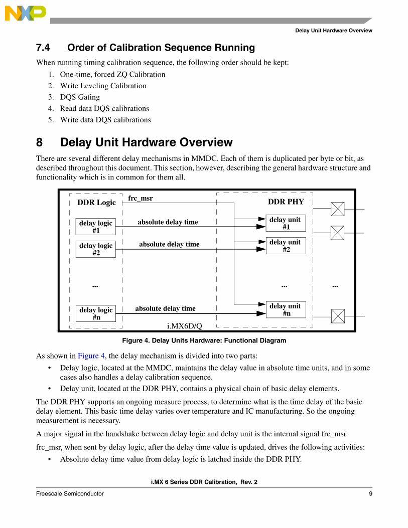
8 Delay Unit Hardware OverviewThere are several different delay mechanisms in MMDC. Each of them is duplicated per byte or bit, as described throughout this document. This section, however, describing the general hardware structure and functionality which is in common for them all.
Figure 4. Delay Units Hardware: Functional Diagram
As shown in Figure 4, the delay mechanism is divided into two parts:
• Delay logic, located at the MMDC, maintains the delay value in absolute time units, and in some cases also handles a delay calibration sequence.
• Delay unit, located at the DDR PHY, contains a physical chain of basic delay elements.
The DDR PHY supports an ongoing measure process, to determine what is the time delay of the basic delay element. This basic time delay varies over temperature and IC manufacturing. So the ongoing measurement is necessary.
A major signal in the handshake between delay logic and delay unit is the internal signal frc_msr.
frc_msr, when sent by delay logic, after the delay time value is updated, drives the following activities:
• Absolute delay time value from delay logic is latched inside the DDR PHY.
i.MX6D/Q
DDR PHYDDR Logic
...
delay logic#1
delay unit#1
delay logic#2
delay unit#2
delay logic#n
delay unit#n
......
absolute delay time
absolute delay time
absolute delay time
frc_msr
i.MX 6 Series DDR Calibration, Rev. 2
10 Freescale Semiconductor
Address and Data Content Used for Timing Calibration
• DDR PHY uses latest measure process to determine how many delay elements should by activated to achieve the required absolute delay time value, and set the delay unit accordingly.
“frc_msr” assertion is thus a must as the terminating stage of a delay calibration. In the auto-initiate and hardware calibration sequence cases, hardware is asserting this signal.
In software handled and forced delay value calibration cases, it is the responsibility of the user to assert this signal, by setting the FRC_MSR bit of the MMDC_MPMUR register, at the end of the calibration sequence.
NOTEIn previous i.MX products, there was a dual delay calibration mechanism, allowing the user to update the delay by programming the absolute time delay value, or by number of delay elements.
In i.MX 6 Series, the latter is no longer available. Only absolute time delay value programming is possible for the user. However, there are read only status registers that allow the user to read the calculated number of delay elements from the DDR PHY:
• MPWLDLST register for Write leveling
• MPDGDLST register for DQS gating
Reading the delay unit numbers is mainly used for IC validation and factory tests. For the MMDC user, this is not a valuable source of information.
9 Address and Data Content Used for Timing CalibrationRead DQS delay, Write DQS delay and DQS gating calibration sequences are all using the same address, data content and compare registers when checking different delay values.
9.1 Address Used in Timing Delay Calibration SequenceThe base address used during read and write operations is hard coded to be (Bank0, Row0, Col0).
In i.MX 6 Series, this is mapped to the DDR device absolute address 0x00000000. This address, however, cannot be accessed externally, as internal i.MX modules are mapped instead. Calibration is thus using the “dummy write and read” mechanism.
By setting the MPSWDAR0[SW_DUMMY_WR] bit, the MMDC accesses this address with no system read or write, and sets the data content as required for the calibration compare.
Before any of the above calibration sequences take place, the user should fill this target address with content matching MMDC_MPPDCMPR1 (i= 0 to 3):
• PDV1[7:0] to [0x00000000 + i * 16]
• PDV1[15:8] to [0x00000004 + i * 16]
• PDV2[7:0] to [0x00000008 + i * 16]
• PDV2[15:8] to [0x0000000c + i * 16]
i.MX 6 Series DDR Calibration, Rev. 2
Freescale Semiconductor 11
ZQ Calibration
NOTEIn i.MX 6 Series, the 0x00000000 address can not be explicitly accessed. Calibration is thus using the “dummy write and read” mechanism. By setting the MPSWDAR0[SW_DUMMY_WR] bit, the MMDC is accessing this address with no system read or write, and set the data content as required for the calibration compare.
9.2 Optimal Data Content for DQS Delay Calibration Sequence• PDV2[15:8] is compared with all 8 data bytes of the 4th and 8th DQS (rising) edges of the
calibrating burst
• PDV2[7:0] is compared with all 8 data bytes of the 3rd and 7th DQS (falling) edges of the calibrating burst
• PDV1[15:8] is compared with all 8 data bytes of the 2nd and 6th DQS (rising) edges of the calibrating burst
• PDV1[7:0] is compared with all 8 data bytes of the 1st and 5th DQS (falling) edges of the calibrating burst
Users are free to program any value to MMDC_MPPDCMPR1. There are, however, two rules for select-ing an effective value:
1. Data must be toggled from rising edge to rising edge, and from falling edge to falling edge (data is separated at IO to 2 stream according to edge).
2. All bits must be toggled in the same direction.
Following these rules, MMDC_MPPDCMPR1 was set to 0x00ffff00, with some systems, this was empirically found to give the best calibration results.
10 ZQ Calibration ZQ calibration is a process that tunes the DRAM and MMDC I/O Pad output drivers (drive strength) and ODT values across changes in process, voltage, and temperature. There are two instances where ZQ calibration is performed: on the i.MX 6 Series (DDR pads) and on the DDR device. ZQ calibration sequence can be initiated as a one-time event, or a periodic sequence.
One-time ZQ calibration can be done in one of the following two ways:
• One-time forced hardware ZQ calibration iterative sequence, as described in detail at Section 10.1, “One-Time Forced Hardware ZQ Calibration Sequence.”
• One-time software handled calibration iterative sequence ZQ calibration, as described in detail at Section 10.2, “One-Time Software ZQ Calibration Sequence.”
Once periodic ZQ calibration (described in detail in Section 10.3, “Auto Initiated Hardware ZQ Calibration Sequence”) is programmed, the MMDC will automatically issue and perform the ZQ calibration without further user interaction. While i.MX 6 Series side periodic calibration is the same at all times, there are two different types of ZQ calibration commands (long and short) that are sent to the DDR device and are described as follows.
i.MX 6 Series DDR Calibration, Rev. 2
12 Freescale Semiconductor
ZQ Calibration
Long DDR device ZQ calibration is initiated upon:
• One time forced ZQ calibration
• i.MX 6 Series power up
• Exiting DDR self refresh mode
• Exiting slow precharge power down
Short DDR device ZQ calibration is initiated when a periodic ZQ is issued.
10.1 One-Time Forced Hardware ZQ Calibration SequenceOne-time ZQ calibration using hardware loop logic is performed by the following sequence:
• Make sure all accesses to DDR are finished.
• Set MMDC register fields according to Table 1.
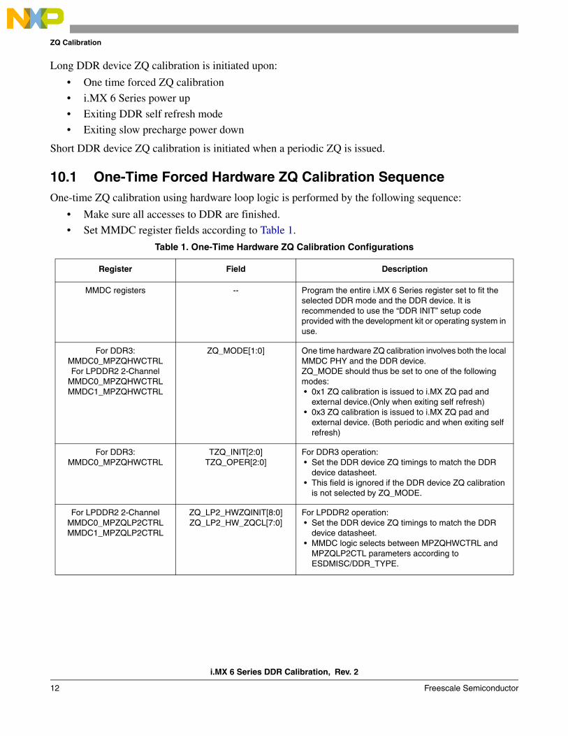
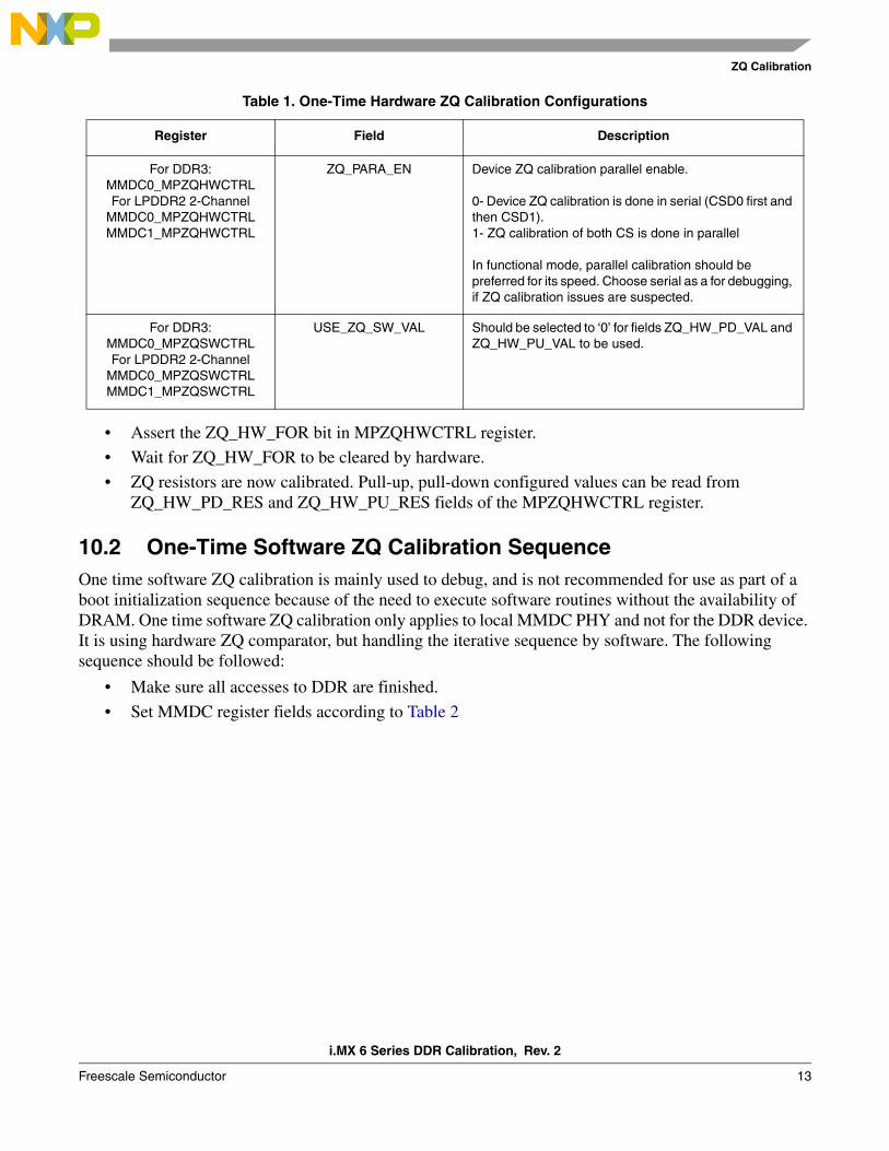
Table 1. One-Time Hardware ZQ Calibration Configurations
Register Field Description
MMDC registers -- Program the entire i.MX 6 Series register set to fit the selected DDR mode and the DDR device. It is recommended to use the “DDR INIT” setup code provided with the development kit or operating system in use.
For DDR3:MMDC0_MPZQHWCTRLFor LPDDR2 2-Channel
MMDC0_MPZQHWCTRLMMDC1_MPZQHWCTRL
ZQ_MODE[1:0] One time hardware ZQ calibration involves both the local MMDC PHY and the DDR device.ZQ_MODE should thus be set to one of the following modes: • 0x1 ZQ calibration is issued to i.MX ZQ pad and
external device.(Only when exiting self refresh) • 0x3 ZQ calibration is issued to i.MX ZQ pad and
external device. (Both periodic and when exiting self refresh)
For DDR3:MMDC0_MPZQHWCTRL
TZQ_INIT[2:0]TZQ_OPER[2:0]
For DDR3 operation: • Set the DDR device ZQ timings to match the DDR
device datasheet. • This field is ignored if the DDR device ZQ calibration
is not selected by ZQ_MODE.
For LPDDR2 2-ChannelMMDC0_MPZQLP2CTRLMMDC1_MPZQLP2CTRL
ZQ_LP2_HWZQINIT[8:0]ZQ_LP2_HW_ZQCL[7:0]
For LPDDR2 operation: • Set the DDR device ZQ timings to match the DDR
device datasheet. • MMDC logic selects between MPZQHWCTRL and
MPZQLP2CTL parameters according to ESDMISC/DDR_TYPE.
i.MX 6 Series DDR Calibration, Rev. 2
Freescale Semiconductor 13
ZQ Calibration
• Assert the ZQ_HW_FOR bit in MPZQHWCTRL register.
• Wait for ZQ_HW_FOR to be cleared by hardware.
• ZQ resistors are now calibrated. Pull-up, pull-down configured values can be read from ZQ_HW_PD_RES and ZQ_HW_PU_RES fields of the MPZQHWCTRL register.
10.2 One-Time Software ZQ Calibration SequenceOne time software ZQ calibration is mainly used to debug, and is not recommended for use as part of a boot initialization sequence because of the need to execute software routines without the availability of DRAM. One time software ZQ calibration only applies to local MMDC PHY and not for the DDR device. It is using hardware ZQ comparator, but handling the iterative sequence by software. The following sequence should be followed:
• Make sure all accesses to DDR are finished.
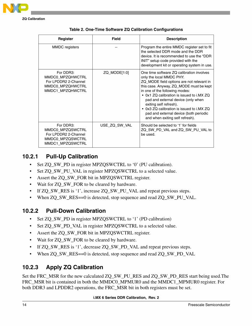
• Set MMDC register fields according to Table 2
For DDR3:MMDC0_MPZQHWCTRLFor LPDDR2 2-Channel
MMDC0_MPZQHWCTRLMMDC1_MPZQHWCTRL
ZQ_PARA_EN Device ZQ calibration parallel enable.
0- Device ZQ calibration is done in serial (CSD0 first and then CSD1).1- ZQ calibration of both CS is done in parallel
In functional mode, parallel calibration should be preferred for its speed. Choose serial as a for debugging, if ZQ calibration issues are suspected.
For DDR3:MMDC0_MPZQSWCTRLFor LPDDR2 2-Channel
MMDC0_MPZQSWCTRLMMDC1_MPZQSWCTRL
USE_ZQ_SW_VAL Should be selected to ‘0’ for fields ZQ_HW_PD_VAL and ZQ_HW_PU_VAL to be used.
Table 1. One-Time Hardware ZQ Calibration Configurations
Register Field Description
i.MX 6 Series DDR Calibration, Rev. 2
14 Freescale Semiconductor
ZQ Calibration
10.2.1 Pull-Up Calibration• Set ZQ_SW_PD in register MPZQSWCTRL to ‘0’ (PU calibration).• Set ZQ_SW_PU_VAL in register MPZQSWCTRL to a selected value.• Assert the ZQ_SW_FOR bit in MPZQSWCTRL register.• Wait for ZQ_SW_FOR to be cleared by hardware.• If ZQ_SW_RES is ‘1’, increase ZQ_SW_PU_VAL and repeat previous steps.• When ZQ_SW_RES==0 is detected, stop sequence and read ZQ_SW_PU_VAL.
10.2.2 Pull-Down Calibration• Set ZQ_SW_PD in register MPZQSWCTRL to ‘1’ (PD calibration)
• Set ZQ_SW_PD_VAL in register MPZQSWCTRL to a selected value.
• Assert the ZQ_SW_FOR bit in MPZQSWCTRL register.
• Wait for ZQ_SW_FOR to be cleared by hardware.
• If ZQ_SW_RES is ‘1’, decrease ZQ_SW_PD_VAL and repeat previous steps.
• When ZQ_SW_RES==0 is detected, stop sequence and read ZQ_SW_PD_VAL
10.2.3 Apply ZQ CalibrationSet the FRC_MSR for the new calculated ZQ_SW_PU_RES and ZQ_SW_PD_RES start being used.The FRC_MSR bit is contained in both the MMDC0_MPMUR0 and the MMDC1_MPMUR0 register. For both DDR3 and LPDDR2 operations, the FRC_MSR bit in both registers must be set.
Table 2. One-Time Software ZQ Calibration Configurations
Register Field Description
MMDC registers -- Program the entire MMDC register set to fit the selected DDR mode and the DDR device. It is recommended to use the “DDR INIT” setup code provided with the development kit or operating system in use.
For DDR3:MMDC0_MPZQHWCTRLFor LPDDR2 2-Channel
MMDC0_MPZQHWCTRLMMDC1_MPZQHWCTRL
ZQ_MODE[1:0] One time software ZQ calibration involves only the local MMDC PHY.ZQ_MODE field options are not relevant in this case. Anyway, ZQ_MODE must be kept in one of the following modes: • 0x1 ZQ calibration is issued to i.MX ZQ
pad and external device (only when exiting self refresh).
• 0x3 ZQ calibration is issued to i.MX ZQ pad and external device (both periodic and when exiting self refresh).
For DDR3:MMDC0_MPZQSWCTRLFor LPDDR2 2-Channel
MMDC0_MPZQSWCTRLMMDC1_MPZQSWCTRL
USE_ZQ_SW_VAL Should be selected to ‘1’ for fields ZQ_SW_PD_VAL and ZQ_SW_PU_VAL to be used.
i.MX 6 Series DDR Calibration, Rev. 2
Freescale Semiconductor 15
ZQ Calibration
10.3 Auto Initiated Hardware ZQ Calibration SequenceAuto initiated ZQ calibration using hardware loop logic is performed by the following sequence:
1. Make sure all accesses to DDR are finished.
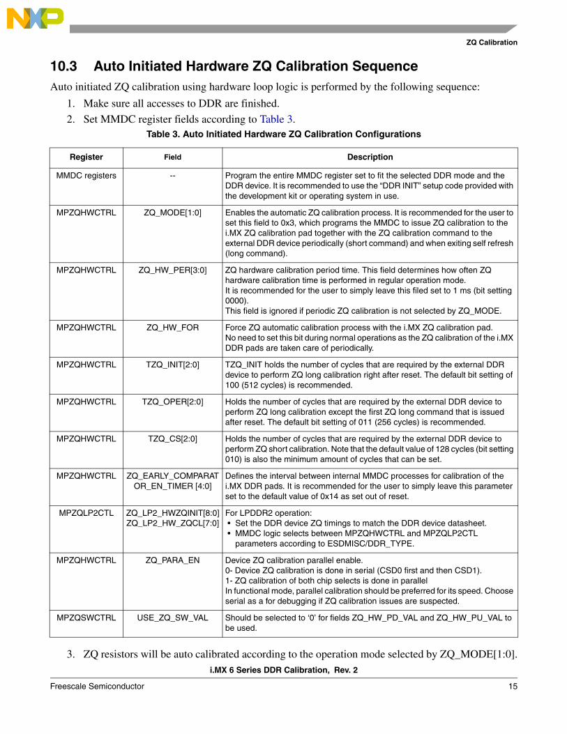
2. Set MMDC register fields according to Table 3.Table 3. Auto Initiated Hardware ZQ Calibration Configurations
3. ZQ resistors will be auto calibrated according to the operation mode selected by ZQ_MODE[1:0].
Register Field Description
MMDC registers -- Program the entire MMDC register set to fit the selected DDR mode and the DDR device. It is recommended to use the “DDR INIT” setup code provided with the development kit or operating system in use.
MPZQHWCTRL ZQ_MODE[1:0] Enables the automatic ZQ calibration process. It is recommended for the user to set this field to 0x3, which programs the MMDC to issue ZQ calibration to the i.MX ZQ calibration pad together with the ZQ calibration command to the external DDR device periodically (short command) and when exiting self refresh (long command).
MPZQHWCTRL ZQ_HW_PER[3:0] ZQ hardware calibration period time. This field determines how often ZQ hardware calibration time is performed in regular operation mode.It is recommended for the user to simply leave this filed set to 1 ms (bit setting 0000). This field is ignored if periodic ZQ calibration is not selected by ZQ_MODE.
MPZQHWCTRL ZQ_HW_FOR Force ZQ automatic calibration process with the i.MX ZQ calibration pad. No need to set this bit during normal operations as the ZQ calibration of the i.MX DDR pads are taken care of periodically.
MPZQHWCTRL TZQ_INIT[2:0] TZQ_INIT holds the number of cycles that are required by the external DDR device to perform ZQ long calibration right after reset. The default bit setting of 100 (512 cycles) is recommended.
MPZQHWCTRL TZQ_OPER[2:0] Holds the number of cycles that are required by the external DDR device to perform ZQ long calibration except the first ZQ long command that is issued after reset. The default bit setting of 011 (256 cycles) is recommended.
MPZQHWCTRL TZQ_CS[2:0] Holds the number of cycles that are required by the external DDR device to perform ZQ short calibration. Note that the default value of 128 cycles (bit setting 010) is also the minimum amount of cycles that can be set.
MPZQHWCTRL ZQ_EARLY_COMPARATOR_EN_TIMER [4:0]
Defines the interval between internal MMDC processes for calibration of the i.MX DDR pads. It is recommended for the user to simply leave this parameter set to the default value of 0x14 as set out of reset.
MPZQLP2CTL ZQ_LP2_HWZQINIT[8:0]ZQ_LP2_HW_ZQCL[7:0]
For LPDDR2 operation: • Set the DDR device ZQ timings to match the DDR device datasheet. • MMDC logic selects between MPZQHWCTRL and MPZQLP2CTL
parameters according to ESDMISC/DDR_TYPE.
MPZQHWCTRL ZQ_PARA_EN Device ZQ calibration parallel enable. 0- Device ZQ calibration is done in serial (CSD0 first and then CSD1).1- ZQ calibration of both chip selects is done in parallelIn functional mode, parallel calibration should be preferred for its speed. Choose serial as a for debugging if ZQ calibration issues are suspected.
MPZQSWCTRL USE_ZQ_SW_VAL Should be selected to ‘0’ for fields ZQ_HW_PD_VAL and ZQ_HW_PU_VAL to be used.
i.MX 6 Series DDR Calibration, Rev. 2
16 Freescale Semiconductor
Write Leveling
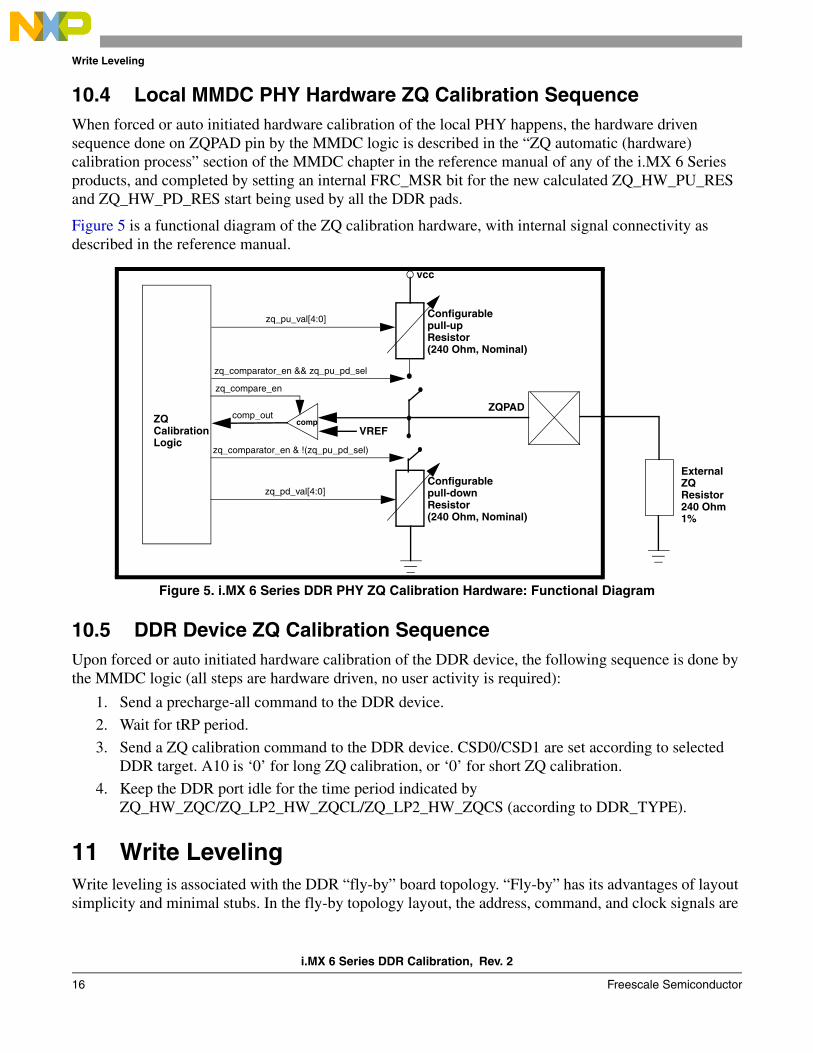
10.4 Local MMDC PHY Hardware ZQ Calibration SequenceWhen forced or auto initiated hardware calibration of the local PHY happens, the hardware driven sequence done on ZQPAD pin by the MMDC logic is described in the “ZQ automatic (hardware) calibration process” section of the MMDC chapter in the reference manual of any of the i.MX 6 Series products, and completed by setting an internal FRC_MSR bit for the new calculated ZQ_HW_PU_RES and ZQ_HW_PD_RES start being used by all the DDR pads.
Figure 5 is a functional diagram of the ZQ calibration hardware, with internal signal connectivity as described in the reference manual.
Figure 5. i.MX 6 Series DDR PHY ZQ Calibration Hardware: Functional Diagram
10.5 DDR Device ZQ Calibration SequenceUpon forced or auto initiated hardware calibration of the DDR device, the following sequence is done by the MMDC logic (all steps are hardware driven, no user activity is required):
1. Send a precharge-all command to the DDR device.
2. Wait for tRP period.
3. Send a ZQ calibration command to the DDR device. CSD0/CSD1 are set according to selected DDR target. A10 is ‘0’ for long ZQ calibration, or ‘0’ for short ZQ calibration.
4. Keep the DDR port idle for the time period indicated by ZQ_HW_ZQC/ZQ_LP2_HW_ZQCL/ZQ_LP2_HW_ZQCS (according to DDR_TYPE).
11 Write LevelingWrite leveling is associated with the DDR “fly-by” board topology. “Fly-by” has its advantages of layout simplicity and minimal stubs. In the fly-by topology layout, the address, command, and clock signals are
ExternalZQResistor240 Ohm
Configurablepull-downResistor(240 Ohm, Nominal)
Configurablepull-upResistor(240 Ohm, Nominal)
vcc
ZQ VREF
comp
zq_pu_val[4:0]
zq_pd_val[4:0]
comp_out
LogicCalibration
zq_comparator_en && zq_pu_pd_sel
zq_comparator_en & !(zq_pu_pd_sel)
1%
zq_compare_en
ZQPAD
i.MX 6 Series DDR Calibration, Rev. 2
Freescale Semiconductor 17
Write Leveling
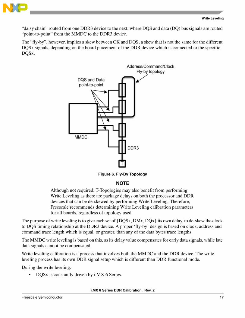
“daisy chain” routed from one DDR3 device to the next, where DQS and data (DQ) bus signals are routed “point-to-point” from the MMDC to the DDR3 device.
The “fly-by”, however, implies a skew between CK and DQS, a skew that is not the same for the different DQSx signals, depending on the board placement of the DDR device which is connected to the specific DQSx.
Figure 6. Fly-By Topology
NOTEAlthough not required, T-Topologies may also benefit from performing Write Leveling as there are package delays on both the processor and DDR devices that can be de-skewed by performing Write Leveling. Therefore, Freescale recommends determining Write Leveling calibration parameters for all boards, regardless of topology used.
The purpose of write leveling is to give each set of {DQSx, DMx, DQx} its own delay, to de-skew the clock to DQS timing relationship at the DDR3 device. A proper ‘fly-by’ design is based on clock, address and command trace length which is equal, or greater, than any of the data bytes trace lengths.
The MMDC write leveling is based on this, as its delay value compensates for early data signals, while late data signals cannot be compensated.
Write leveling calibration is a process that involves both the MMDC and the DDR device. The write leveling process has its own DDR signal setup which is different than DDR functional mode.
During the write leveling:
• DQSx is constantly driven by i.MX 6 Series.
i.MX 6 Series DDR Calibration, Rev. 2
18 Freescale Semiconductor
Write Leveling
• DQx is constantly driven by the DDR device.
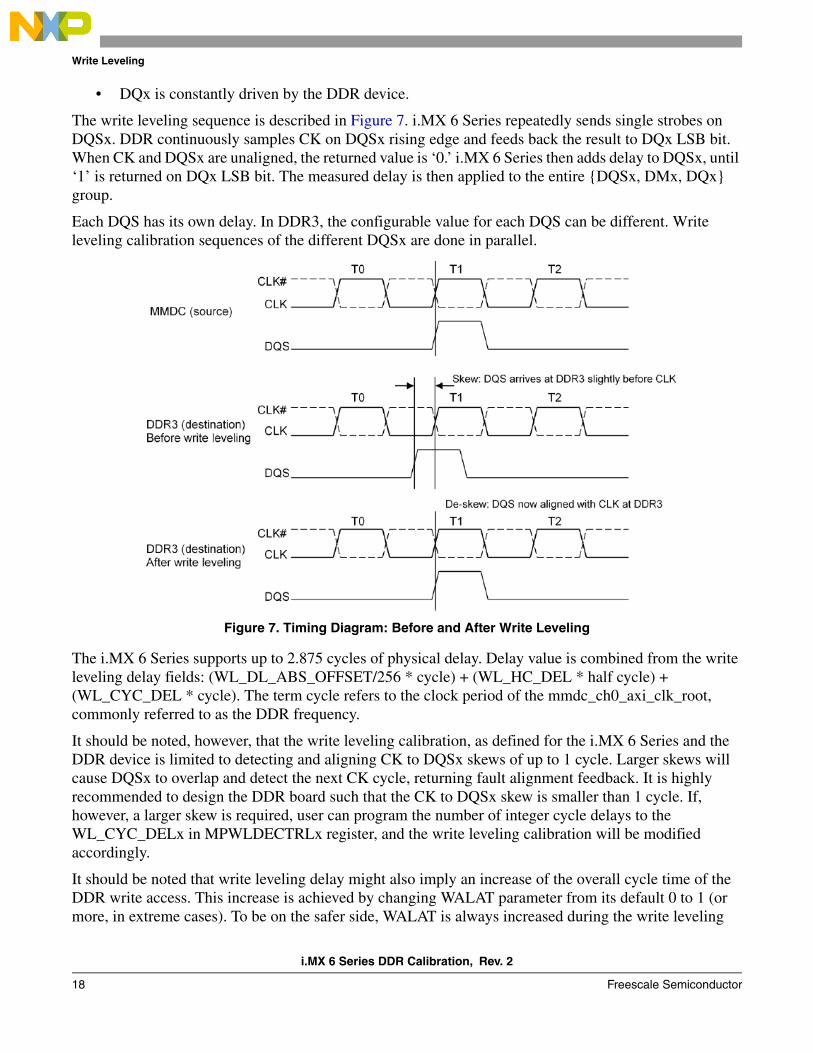
The write leveling sequence is described in Figure 7. i.MX 6 Series repeatedly sends single strobes on DQSx. DDR continuously samples CK on DQSx rising edge and feeds back the result to DQx LSB bit. When CK and DQSx are unaligned, the returned value is ‘0.’ i.MX 6 Series then adds delay to DQSx, until ‘1’ is returned on DQx LSB bit. The measured delay is then applied to the entire {DQSx, DMx, DQx} group.
Each DQS has its own delay. In DDR3, the configurable value for each DQS can be different. Write leveling calibration sequences of the different DQSx are done in parallel.
Figure 7. Timing Diagram: Before and After Write Leveling
The i.MX 6 Series supports up to 2.875 cycles of physical delay. Delay value is combined from the write leveling delay fields: (WL_DL_ABS_OFFSET/256 * cycle) + (WL_HC_DEL * half cycle) + (WL_CYC_DEL * cycle). The term cycle refers to the clock period of the mmdc_ch0_axi_clk_root, commonly referred to as the DDR frequency.
It should be noted, however, that the write leveling calibration, as defined for the i.MX 6 Series and the DDR device is limited to detecting and aligning CK to DQSx skews of up to 1 cycle. Larger skews will cause DQSx to overlap and detect the next CK cycle, returning fault alignment feedback. It is highly recommended to design the DDR board such that the CK to DQSx skew is smaller than 1 cycle. If, however, a larger skew is required, user can program the number of integer cycle delays to the WL_CYC_DELx in MPWLDECTRLx register, and the write leveling calibration will be modified accordingly.
It should be noted that write leveling delay might also imply an increase of the overall cycle time of the DDR write access. This increase is achieved by changing WALAT parameter from its default 0 to 1 (or more, in extreme cases). To be on the safer side, WALAT is always increased during the write leveling
i.MX 6 Series DDR Calibration, Rev. 2
Freescale Semiconductor 19
Write Leveling
calibration process (see Section 11.2, “Hardware Write Leveling Calibration Sequence”). If resulted write leveling delays are small (less than 10% of a clock period), WALAT can be written back to 0, for the DDR normal operation. If, on the other hand, write leveling delays are significant (greater than 10% of a clock cycle per JEDEC standards), increased WALAT should be kept as part of the new DDR setup that include the newly calculated write leveling delays. Increased WALAT implies a small degradation in DDR port performance.
NOTEThe WALAT value set in register MDMISC has no effect on the value determined by the write leveling calibration sequence since WALAT only applies full clock cycles and the write level calibration sequence can only align the strobe sequence to a fraction of a clock cycle (< one full cycle).
Write leveling calibration is done using devices connected to CSD0 or to CDS1. Selecting between the two is done by proper setting of MDMISC[CALIB_PER_CS] and MDSCR[CMD_CS] bits. Applying calibration results to a board populated with DDR devices on both CSD0 and CSD1, is conditioned by keeping board layout rules, as described in Section 5, “Calibration and Chip Selects.”
i.MX 6 Series write leveling calibration senses the LSB of each DQx byte for the write leveling feedback. That means, bits 0, 8, 16, and 24 (as well as 32, 40, 48, and 56, when 64-bits DDR3) of the DQ bus are being used. These bits are known as the prime data bits of a byte lane. This fact should be considered during board design. Regularly, board design is allowed to swap bit connections within the DDR byte, wherever it helps DDR route optimization. Swapping prime data bits, as above, will disable operation of the write leveling calibration. Swapping the prime data bits should be avoided, unless using a DDR device that reflects write leveling feedback to all bits of the DQx byte.
11.1 Calibrating Write Leveling with a Preset Delay ValueThe write leveling delay parameters can be set without running the calibration sequence, by programming a preset value of absolute delay.
The source of the preset value can be a write leveling calibration sequence done in the past. Alternately, the delay values can be a manual estimation of data delays based on DDR board route lengths.
The following empirical rule, based on simulations and board experience, can be used:
Each ([SDCLK_LENGTH] -[DQS_LENGTH])/6, measured in inches, implies 1 ns of delay.
The time delay received by this rule should be converted to ddr_cycle/256 units, converted to hexadecimal, and applied to a delay register.
Calibrating with a preset value is done by the following:
• Write the write leveling preset value to MMDC0_MPWLDECTRL0, MMDC0_MPWLDECTRL1, MMDC1_MPWLDECTRL0, and MMDC1_MPWLDECTRL1 registers.
• Set MMDC0_MPMUR[FRC_MSR], and MMDC1_MPMUR[FRC_MSR] bits.
i.MX 6 Series DDR Calibration, Rev. 2
20 Freescale Semiconductor
Write Leveling
11.2 Hardware Write Leveling Calibration Sequence The Hardware Write Leveling Calibration Sequence can be executed during prototype development, on the factory floor as part of a Factory Acceptance Test (FAT), or during a system boot sequence. To perform this sequence, the following steps should be executed by user code:
1. Store the contents originally programming in the DDR3 MR1 register. This register will be overwritten in step 3 to enter write leveling mode (DDR3 device does not allow read of the mode registers, so MR1 content cannot be retrieved by read). Refer to the DDR3 device datasheet for details on the MR1 register.
2. Disable Auto initiated ZQ calibration and DDR auto refresh, so these processes would not interfere with the write leveling calibration.
3. Increase WALAT and RALAT parameters to maximum.
4. Configure the external DDR device to enter write leveling mode through MRS command.
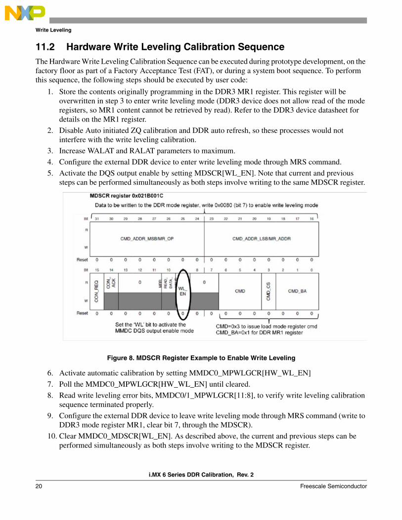
5. Activate the DQS output enable by setting MDSCR[WL_EN]. Note that current and previous steps can be performed simultaneously as both steps involve writing to the same MDSCR register.
Figure 8. MDSCR Register Example to Enable Write Leveling
6. Activate automatic calibration by setting MMDC0_MPWLGCR[HW_WL_EN]
7. Poll the MMDC0_MPWLGCR[HW_WL_EN] until cleared.
8. Read write leveling error bits, MMDC0/1_MPWLGCR[11:8], to verify write leveling calibration sequence terminated properly.
9. Configure the external DDR device to leave write leveling mode through MRS command (write to DDR3 mode register MR1, clear bit 7, through the MDSCR).
10. Clear MMDC0_MDSCR[WL_EN]. As described above, the current and previous steps can be performed simultaneously as both steps involve writing to the MDSCR register.
i.MX 6 Series DDR Calibration, Rev. 2
Freescale Semiconductor 21
DQS Gating
11. Configure MMDC to functional mode DDR parameters: RALAT, WALAT, auto ZQ calibration and auto refresh.
12. Once this process is done, the MMDC0/1_MPWLDECTRL0 and MMDC0/1_MPWLDECTRL1 registers are updated with the proper write leveling delays. These values can be kept and reused in future, as described in Section 11.1, “Calibrating Write Leveling with a Preset Delay Value.”
After MMDC0_MPWLGCR[HW_WL_EN] bit is activated (step 6), the steps executed automatically by the MMDC are described in the “Hardware write leveling calibration” section of the MMDC chapter in the reference manual of any of the i.MX 6 Series products.
11.3 Write Leveling Software Calibration SequenceThe Write Leveling software calibration is accomplished by user code as described in the “Software Write Leveling calibration” section of the MMDC chapter in the reference manual of any of the i.MX 6 series products. The software sequence can be performed during the prototype testing phase of the board, and can provide more accurate values than the hardware method, but it takes considerably longer to perform a software sequence. Using the software method as part of FAT testing would add extra time to the final manufacturing test, and using the software method at boot is not recommended. (The note in the Reference Manual refers to using software calibration during boot only.)
12 DQS GatingThe read DQS gating calibration is not mandatory by DDR3 JEDEC standard, but it is a required mechanism to determine the valid time period with which to begin sampling the incoming “read” DQS signal. The intent is to avoid inadvertently sampling an invalid DQS state, such as misinterpreting the initial High-Z to logic low transition as a valid read DQS edge.
DQS gating is thus an over-time masking operation of the input DQS driven by the DDR device. DQS gating assertion is done according to the DQS gating delay, as configured to the MMDC registers. DQS gating negation has a fixed timing after the negedge of last DQS strobe (if there is no back to back access).
i.MX 6 Series DDR Calibration, Rev. 2
22 Freescale Semiconductor
DQS Gating
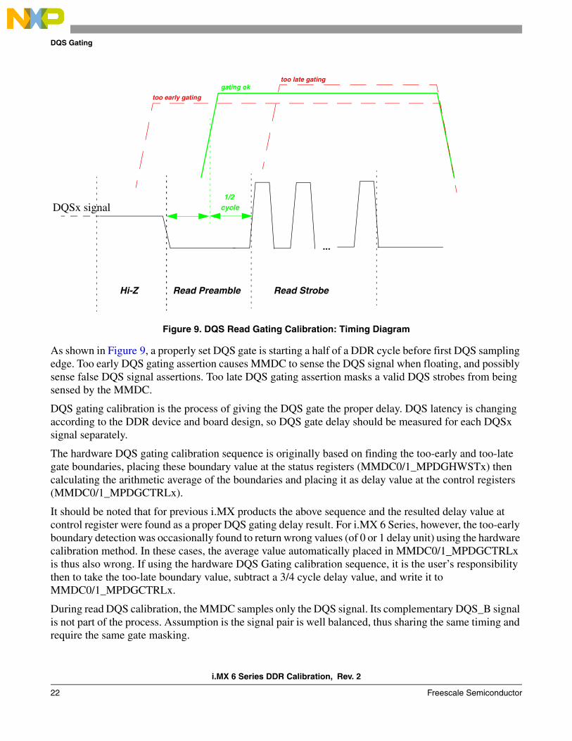
Figure 9. DQS Read Gating Calibration: Timing Diagram
As shown in Figure 9, a properly set DQS gate is starting a half of a DDR cycle before first DQS sampling edge. Too early DQS gating assertion causes MMDC to sense the DQS signal when floating, and possibly sense false DQS signal assertions. Too late DQS gating assertion masks a valid DQS strobes from being sensed by the MMDC.
DQS gating calibration is the process of giving the DQS gate the proper delay. DQS latency is changing according to the DDR device and board design, so DQS gate delay should be measured for each DQSx signal separately.
The hardware DQS gating calibration sequence is originally based on finding the too-early and too-late gate boundaries, placing these boundary value at the status registers (MMDC0/1_MPDGHWSTx) then calculating the arithmetic average of the boundaries and placing it as delay value at the control registers (MMDC0/1_MPDGCTRLx).
It should be noted that for previous i.MX products the above sequence and the resulted delay value at control register were found as a proper DQS gating delay result. For i.MX 6 Series, however, the too-early boundary detection was occasionally found to return wrong values (of 0 or 1 delay unit) using the hardware calibration method. In these cases, the average value automatically placed in MMDC0/1_MPDGCTRLx is thus also wrong. If using the hardware DQS Gating calibration sequence, it is the user’s responsibility then to take the too-late boundary value, subtract a 3/4 cycle delay value, and write it to MMDC0/1_MPDGCTRLx.
During read DQS calibration, the MMDC samples only the DQS signal. Its complementary DQS_B signal is not part of the process. Assumption is the signal pair is well balanced, thus sharing the same timing and require the same gate masking.
...
DQSx signal
Hi-Z Read Preamble Read Strobe
too early gating
too late gatinggating ok
1/2 cycle
i.MX 6 Series DDR Calibration, Rev. 2
Freescale Semiconductor 23
DQS Gating
Each of the eight DQS signals has a it own gating delay and gating calibration. The DQS gating calibration sequence, however, can be done for all DQSx signals in parallel.
The DQS gating includes a delay of up to seven cycles. Delay value is combined from the DQS gating delay fields: (DG_DL_ABS_OFFSET/256 * cycle) + (DG_HC_DEL * half cycle). The term cycle refers to the clock period of the mmdc_ch0_axi_clk_root, commonly referred to as the DDR frequency.
It should be noted that in order to mask out fault incoming DQS strobes, there is an alternative to DQS gating, by simply applying pull-downs to DQS signals. Pull-downs, however, have their disadvantages, which are excessive power consumption and interference with ODT resistors. DQS gating is free from these, and hence considered as a better choice.
12.1 Calibrating DQS Gating with a Preset Delay ValueDQS gating timing parameters can be set without running the calibration sequence, by programming a preset value of absolute delay.
Preset value source can be a DQS gating calibration sequence done in the past, or any other value estimated by user to optimize DQS gating location.
Calibrating with a preset value is done by the following:
1. Write the DQS gating preset value to MMDC0/1_MPDGCTRL0, MMDC0/1_MPDGCTRL1 registers.
2. Set MMDC0/1_MPMUR[FRC_MSR] bits.
12.2 Hardware DQS Gating Calibration SequenceDQS gating calibration can be done using devices connected to CSD0 or to CDS1. Selecting between the two is done by proper setting of MDMISC[CALIB_PER_CS] and MDSCR[CMD_CS] bits. Applying calibration results to a board populated with DDR devices on both CSD0 and CSD1, is conditioned by keeping board layout rules, as described in Section 5, “Calibration and Chip Selects.”
To perform a hardware DQS calibration sequence, the following steps should be executed:
1. Precharge all active banks (Can be done through MDSCR) as required by the standard.
2. Enter the DDR device into the MPR mode through MRS commands.
3. Configure the MMDC to work with MPR mode by asserting MPPDCMPR2[MPR_CMP].
4. Make sure that the initial value that is configured in the read delay line absolute offset of each byte (i.e. MPRDDLCTL[RD_DL_ABS_OFFSET#]) will place the read DQS somewhere inside the read DQ window.
5. Start the calibration process by asserting MPDGCTRL0[HW_DG_EN].
i.MX 6 Series DDR Calibration, Rev. 2
24 Freescale Semiconductor
DQS Gating
12.3 MMDC Registers Setup for DQS Gating Calibration Sequence
12.3.1 Register Setup Prior to DQS Gating Calibration SequenceSet MMDC register fields according to Table 4:
Table 4. Hardware DQS Gating Calibration Configurations
12.3.2 Calibration Sequence Setup with Predefined Data ContentWhen the predefined mode is used, (MPPDCMPR2[MPR_CMP]) is cleared, then the following steps should be executed:
1. Issue two resets to the read data FIFO through the MPDGCTRL0 register by writing to the RST_RD_FIFO bit (MPDGCTRL0[RST_RD_FIFO]=1) polling this bit to clear for completion of reset, and then repeat this sequence one more time. This sequence must be performed twice in order to properly reset the read data FIFO.
2. Precharge all active banks (Can be done through MMDC0/1_MDSCR) as required by the standard.
— To issue a Precharge-All to CS0, write 0x04000050 to MDSCR.
— To issue a Precharge-All to CS1, write 0x04000058 to MDSCR.
3. Configure the predefined value (specified above as 0x00FFFF00), which reflects the value that will be written and compared through the read calibration, to MPPDCMPR1[PDV1, PDV2].
Register Field Description
i.MX 6 Series registers
-- Program the entire i.MX 6 Series register set to fit the selected DDR mode and the DDR device. It is recommended to use the “DDR INIT” setup code provided with the development kit or operating system in use.
IOMUXC/SW_PAD_CTL_DQSx
pke,pue,pus
Set to Active pull-up.
MPDGCTRL0 DG_EXT_UP DG extend upper boundary. ‘0’ - Upper boundary of DQS gating hardware calibration is set according to first fail
after at least one pass. ‘1’ - Upper boundary is set according to the last pass.
There is no significant difference observed in calibration results due to this bit setup. It is typically remains clear.
MPDGCTRL0 DG_DIS Keep DG_DIS cleared for the DQS gating to take place. Contrary to some early versions of the reference manual, DG_DIS is a writable bit.
MPDGCTRL0 DG_CMP_CYC ‘0’ PHY compares the received data 16 cycles after sending the read command‘1’ PHY compares the received data 32 cycles after sending the read commandFor the final DQS gating sequence procedure, use the faster 16 cycle delay.Use the 32 cycle delay for initial operation and debugging of the DQS gating sequence. Contrary to some early versions of the reference manual, DG_CMP_CYC is a writable bit.
MDMISC WALAT,RALAT
Increase WALAT and RALAT parameters to maximum.
i.MX 6 Series DDR Calibration, Rev. 2
Freescale Semiconductor 25
DQS Gating
4. Issue a write access to the external DDR device by setting the bit SW_DUMMY_WR (bit 0) in the MPSWDAR0. This will cause the MMDC to generate a write access with the data programmed in the MPPDCMPR1 register towards the chip select that is defined in MDMISC[CALIB_PER_CS].
5. Poll the SW_DUMMY_WR bit until it clears to indicate completion of the write access.
6. Make sure that the initial value that is configured in the read delay line absolute offset of each byte (MPRDDLCTL[RD_DL_ABS_OFFSET#]) will place the read DQS somewhere inside the read DQ window. Note that the default value of 0x40 should be sufficient so no action is necessary by the user, unless the user has changed these values prior to the calibration process.
7. Start the calibration process by asserting MPDGCTRL0[HW_DG_EN]. The MMDC will then perform the hardware sequence as described in the “Hardware DQS calibration with predefined value” section of the MMDC chapter in the reference manual of any of the i.MX 6 Series products.
8. Poll the MPDGCTRL0[HW_DG_EN] until it is cleared to indicate the completion of the hardware calibration. Also, check MMDC0/1_MPDGCTRL0[HW_DG_ERR] in both PHYs to see if any errors occurred during calibration.
9. For each of the DQSx:
— Read the HW_DG_UPx value from the MMDC0/1_MPDGHWSTx, subtract the value of 0xc0 (3/4 cycle).
— Write 7 LSBs of the result to MMDC0/1_MPDGCTRLx[DG_DL_ABS_OFFSETx]
— Write 4 MSBs of the result to MMDC0/1_MPDGCTRLx[DG_HC_DELx]
10. Result DQS gating delay values are now valid on the MMDC0/1_MPDGCTRL0 and MPDGCTRL1 registers. Their contents can be read and saved for future delay setup.
11. Configure DDR setup to functional mode. This includes MDMISC[RALAT, WALAT] and disabling DQS pull-ups.
12.4 DQS Gating Software Calibration SequenceDQS gating software calibration is accomplished by user code as described in the “Software read DQS gating calibration” section of the MMDC chapter in the reference manual of any of the i.MX 6 Series products. The software sequence can be performed during the prototype testing phase of the board, and can provide more accurate values than the hardware method, but it takes considerably longer to perform a software sequence. Because the software method can be more accurate than the hardware method, it may only be necessary to subtract a 1/2-cycle delay from the maximum determined value. Using the software method as part of FAT testing would add extra time to the final manufacturing test, and using the software method at boot is not recommended. (The note in the Reference Manual refers to using software calibration during boot only.)
i.MX 6 Series DDR Calibration, Rev. 2
26 Freescale Semiconductor
Read DQS Delay Calibration
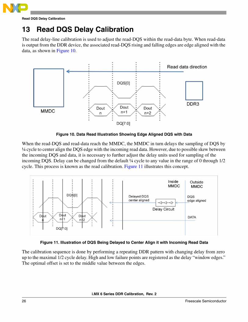
13 Read DQS Delay CalibrationThe read delay-line calibration is used to adjust the read-DQS within the read-data byte. When read-data is output from the DDR device, the associated read-DQS rising and falling edges are edge aligned with the data, as shown in Figure 10.
Figure 10. Data Read Illustration Showing Edge Aligned DQS with Data
When the read-DQS and read-data reach the MMDC, the MMDC in turn delays the sampling of DQS by ¼ cycle to center align the DQS edge with the incoming read data. However, due to possible skew between the incoming DQS and data, it is necessary to further adjust the delay units used for sampling of the incoming DQS. Delay can be changed from the default ¼ cycle to any value in the range of 0 through 1/2 cycle. This process is known as the read calibration. Figure 11 illustrates this concept.
Figure 11. Illustration of DQS Being Delayed to Center Align it with Incoming Read Data
The calibration sequence is done by performing a repeating DDR pattern with changing delay from zero up to the maximal 1/2 cycle delay. High and low failure points are registered as the delay “window edges.” The optimal offset is set to the middle value between the edges.
i.MX 6 Series DDR Calibration, Rev. 2
Freescale Semiconductor 27
Read DQS Delay Calibration
There are a total of eight (8) or four (4) read delay circuits, one per DQS signal, according to the number of data bytes in operating mode. Upon completion of the read calibration, MMDC0/1_MPRDDLCTLx registers hold the absolute read delay for each DQS.
NOTEWhen calibrating the read delay line, the starting configuration value must be a valid middle value (so data can be written and read in this case) though it might not be the optimal value. The delay line calibration should be done after DQS gating and write level (for a ‘fly-by’ DDR3 board topology) calibrations.
13.1 Calibrating Read DQS with a Preset Delay ValueThe read DQS delay parameters can be set without running the calibration sequence, by programming a preset value of absolute delay value.
The source of the preset value can be a read DQS calibration done in the past, or any other value estimated by user to optimize read DQS signal location.
Calibrating with a preset value is done by the following:
1. Write the read DQS preset value to MMDC0/1_MPRDDLCTL registers
2. Set MMDC0/1_MPMUR[FRC_MSR] bit
13.2 Read DQS Delay Line Calibration SequenceRead DQS delay calibration can be done using devices connected to CSD0 or to CDS1. Selecting between the two is done by proper setting of MDMISC[CALIB_PER_CS] and MDSCR[CMD_CS] bits. Applying calibration results to a board populated with DDR devices on both CSD0 and CSD1, is conditioned by keeping board layout rules, as described in Section 5, “Calibration and Chip Selects.”
To perform a read DQS calibration sequence, the following steps should be executed:
1. Precharge all active banks (Can be done through MDSCR) as required by the standard.
2. Enter the DDR device into the MPR/DQ mode through MRS/MRW commands.
3. Configure the MMDC to work with MPR/DQ mode by asserting MPPDCMPR2[MPR_CMP].
4. Make sure that the initial value that is configured in the read delay line absolute offset of each byte (i.e. MPRDDLCTL[RD_DL_ABS_OFFSET#]) will place the read DQS somewhere inside the read DQ window.
5. Start the calibration process by asserting MPRDDLHWCTL[HW_RD_DL_EN].
i.MX 6 Series DDR Calibration, Rev. 2
28 Freescale Semiconductor
Read DQS Delay Calibration
13.2.1 Calibration Sequence Setup with Predefined Data ContentWhen the predefined mode is used, (MPPDCMPR2[MPR_CMP]) is cleared, then the following steps should be executed:
1. Increase MDMISC[WALAT, RALAT] to maximum.
2. Configure SW_PAD_CTL_DRAM_SDQSx registers to active pull-ups on DQS signals.
3. Issue two resets to the read data FIFO through the MPDGCTRL0 register by writing to the RST_RD_FIFO bit (MPDGCTRL0[RST_RD_FIFO]=1) polling this bit to clear for completion of reset, and then repeat this sequence one more time. This sequence must be performed twice in order to properly reset the read data FIFO.
4. Precharge all active banks (through MDSCR) as required by the standard:
— To issue a Precharge-All to CS0, write 0x04000050 to MDSCR.
— To issue a Precharge-All to CS1, write 0x04000058 to MDSCR.
5. Configure the predefined value (specified above as 0x00FFFF00), which reflects the value that will be written and compared through the read calibration, to MPPDCMPR1[PDV1, PDV2]
6. Issue a write access to the external DDR device by setting the bit SW_DUMMY_WR (bit 0) in the MPSWDAR0. This will cause the MMDC to generate a write access with the data programmed in the MPPDCMPR1 register towards the chip select that is defined in MDMISC[CALIB_PER_CS].
7. Poll the SW_DUMMY_WR bit until it clears to indicate completion of the write access.
8. Make sure that the initial value that is configured in the read delay line absolute offset of each byte (MPRDDLCTL[RD_DL_ABS_OFFSET#]) will place the read DQS somewhere inside the read DQ window. Note that the default value of 0x40 should be sufficient, so no action is necessary by the user, unless the user has changed these values prior to the calibration process.
9. Start the calibration process by asserting MMDC0/1_MPRDDLHWCTL[HW_RD_DL_EN]. The MMDC will then perform the hardware sequence as described in the “Hardware (automatic) calibration with predefined value” section of the MMDC chapter in the reference manual of any of the i.MX 6 Series products.
10. Poll MMDC0/1_MPRDDLHWCTL[HW_RD_DL_EN] until this bit clears to indicate completion. Also, check MMDC0_MPRDDLHWCTL[HW_RD_DL_ERR3, HW_RD_DL_ERR2, HW_RD_ DL_ERR1, and HW_RD_ DL_ERR0] in both PHYs to see if any errors occurred during calibration.
11. After hardware calibration, result DQS read delay values are valid in the MMDC0/1_MPRDDLCTL registers. The contents can be read and saved for future delay setup. For debug purpose, the Read DQS window high and low edges are also valid in the MMDC0/1_MPRDDLHWSTx registers.
12. Configure DDR setup to functional mode. This includes MDMISC[RALAT, WALAT] and disables DQS pull-ups.
13.2.2 DQS Read Calibration Software SequenceRead DQS software calibration is accomplished by user code as described in the “Software read calibration” section of the MMDC chapter in the reference manual of any of the i.MX 6 Series products.
i.MX 6 Series DDR Calibration, Rev. 2
Freescale Semiconductor 29
Write DQS Delay Calibration
The software sequence can be performed during the prototype testing phase of the board, and can provide more accurate values than the hardware method, but it takes considerably longer to perform a software sequence. Using the software method as part of FAT testing would add extra time to the final manufacturing test, and using the software method at boot is not recommended. (The note in the Reference Manual refers to using software calibration during boot only.)
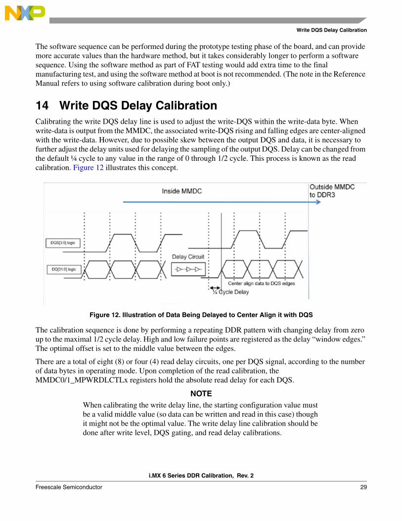
14 Write DQS Delay CalibrationCalibrating the write DQS delay line is used to adjust the write-DQS within the write-data byte. When write-data is output from the MMDC, the associated write-DQS rising and falling edges are center-aligned with the write-data. However, due to possible skew between the output DQS and data, it is necessary to further adjust the delay units used for delaying the sampling of the output DQS. Delay can be changed from the default ¼ cycle to any value in the range of 0 through 1/2 cycle. This process is known as the read calibration. Figure 12 illustrates this concept.
Figure 12. Illustration of Data Being Delayed to Center Align it with DQS
The calibration sequence is done by performing a repeating DDR pattern with changing delay from zero up to the maximal 1/2 cycle delay. High and low failure points are registered as the delay “window edges.” The optimal offset is set to the middle value between the edges.
There are a total of eight (8) or four (4) read delay circuits, one per DQS signal, according to the number of data bytes in operating mode. Upon completion of the read calibration, the MMDC0/1_MPWRDLCTLx registers hold the absolute read delay for each DQS.
NOTEWhen calibrating the write delay line, the starting configuration value must be a valid middle value (so data can be written and read in this case) though it might not be the optimal value. The write delay line calibration should be done after write level, DQS gating, and read delay calibrations.
i.MX 6 Series DDR Calibration, Rev. 2
30 Freescale Semiconductor
Write DQS Delay Calibration
14.1 Calibrating Write DQS with a Preset Delay ValueThe write DQS delay parameters can be set without running the calibration sequence, by programming a preset value of absolute delay.
The source of the preset value can be a write DQS calibration done in the past, or any other value estimated by user to optimize write DQS signal location.
Calibrating with a preset value is done by the following:
1. Write the write DQS preset value to MPWRDLCTL register.
2. Set MPMUR[FRC_MSR] bit.
14.2 Hardware Write DQS Delay Line Calibration SequenceWrite DQS delay calibration can be done using devices connected to CSD0 or to CDS1. Selecting between the two is done by proper setting of MDMISC[CALIB_PER_CS] and MDSCR[CMD_CS] bits. Applying calibration results to a board populated with DDR devices on both CSD0 and CSD1, is conditioned by keeping board layout rules, as described in Section 5, “Calibration and Chip Selects.”
To perform a write DQS calibration sequence, the following steps should be executed:
1. Make sure that the initial value that is configured in the write delay line absolute offset of each byte (i.e. MPWRDLCTL[WR_DL_ABS_OFFSET#]) will place the write DQS somewhere inside the write DQ window.
2. Configure the pre-defined value, which reflects the value that will be written and compared through the write calibration, to MPPDCMPR1[PDV1,PDV2].
3. Start the calibration process by asserting MPWRDLHWCTL0[HW_WR_DL_EN].
14.2.1 Calibration Setup with Predefined Data ContentWhen the predefined mode is used, (MPPDCMPR2[MPR_CMP]) is cleared, then the following steps should be executed:
1. Increase MDMISC[WALAT, RALAT] to maximum.
2. Configure SW_PAD_CTL_DRAM_SDQSx registers to active pull-ups on DQS signals.
3. Issue two resets to the read data FIFO through the MPDGCTRL0 register by writing to the RST_RD_FIFO bit (MPDGCTRL0[RST_RD_FIFO]=1) polling this bit to clear for completion of reset, and then repeat this sequence one more time. This sequence must be performed twice in order to properly reset the read data FIFO.
4. Precharge all active banks (through MDSCR) as required by the standard:
— To issue a Precharge-All to CS0, write 0x04000050 to MDSCR.
— To issue a Precharge-All to CS1, write 0x04000058 to MDSCR.
5. Configure the predefined value (specified above as 0x00FFFF00), which reflects the value that will be written and compared through the read calibration, to MPPDCMPR1[PDV1, PDV2]
i.MX 6 Series DDR Calibration, Rev. 2
Freescale Semiconductor 31
Read Data Bit Delay Calibration
6. Issue a write access to the external DDR device by setting the bit SW_DUMMY_WR (bit 0) in the MPSWDAR0. This will cause the MMDC to generate a write access with the data programmed in the MPPDCMPR1 register towards the chip select that is defined in MDMISC[CALIB_PER_CS].
7. Poll the SW_DUMMY_WR bit until it clears to indicate completion of the write access.
8. Make sure that the initial value that is configured in the write delay line absolute offset of each byte (MPWRDLCTL[WR_DL_ABS_OFFSET#]) will place the write DQS somewhere inside the write DQ window. Note that the default value of 0x40 should be sufficient so no action is necessary by the user, unless the user has changed these values prior to the calibration process.
9. Start the calibration process by asserting HW_WR_DL_EN. The MMDC will then perform the hardware sequence as described in the “Hardware (automatic) write calibration” section of the MMDC chapter in the reference manual of any of the i.MX 6 Series products.
10. Poll MMDC0/1_MPWRDLHWCTL[HW_WR_DL_EN] until this bit clears to indicate completion. Also, check MMDC0/1_MPWRDLHWCTL[HW_WR_DL_ERR3, HW_WR_DL_ERR2, HW_WR_ DL_ERR1, HW_WR_ DL_ERR0] in both PHYs to see if any errors occurred during calibration.
11. Result DQS write delay values are now valid in the MPWRDLCTL register. The contents can be read and saved for future delay setup. In addition, for debug information, the upper and lower boundaries for each byte found during the calibration process can be found in the MMDC0/1_MPWRDLHWSTx registers.
12. Configure DDR setup to functional mode. This includes MDMISC[RALAT, WALAT] and disables DQS pull-ups.
14.2.2 Write DQS Software Delay Line Calibration SequenceWrite DQS software calibration is accomplished by user code as described in the “Software write calibration” section of the MMDC chapter in the reference manual of any of the i.MX 6 Series products. The software sequence can be performed during the prototype testing phase of the board, and can provide more accurate values than the hardware method, but it takes considerably longer to perform a software sequence. Using the software method as part of FAT testing would add extra time to the final manufacturing test, and using the software method at boot is not recommended. (The note in the Reference Manual refers to using software calibration during boot only.)
15 Read Data Bit Delay CalibrationRead fine tuning is an additional circuit that enables the option to fine tune the timing of the DQ/DM bits (relative to DQS).
The i.MX 6 Series design is optimized of the setup value of ‘3’ for all the read data bit delay fields, and this is the recommended DDR setup for all i.MX 6 Series boards.
If, however, a trace length and skew issue is detected on a specific board design, it is possible to mitigate this by changing the bit delay accordingly. One unit delay makes a change of approximately 15 ps in signal timing. It is thus possible to set a delay of up to 105 ps, using the full range of 0 to 7 in the bit delay field.
i.MX 6 Series DDR Calibration, Rev. 2
32 Freescale Semiconductor
Write Data Bit Delay Calibration
There is no hardware calibration sequence to determine the optimal bit delay values. The user should test for best DDR performance, trying different values of bit delay.
16 Write Data Bit Delay CalibrationWrite fine tuning is an additional circuit that enables the option to fine tune the timing of the DQ/DM bits (relative to DQS).
The i.MX 6 Series design is optimized of the setup value of ‘0’ for all the write data bit delay fields, and this is the recommended DDR setup for all i.MX 6 Series boards.
If, however, a trace length and skew issue is detected on a specific board design, it is possible to mitigate this by changing the bit delay accordingly. One unit delay makes a change of approximately 15 ps in signal timing. It is thus possible to set a delay of up to 45 ps, using the full range of 0 to 3 in the bit delay field.
There is no hardware calibration sequence to determine the optimal bit delay values. The user should test for best DDR performance, trying different values of bit delay.
17 Clock Delay CalibrationSDCLK signal can be added 0 to 3 delay units relative to all other DDR signals. Delay units are added at the trace pads and are fixed values (i.e, not dependent on MMDC clock frequency). Each delay unit has a nominal value of 15 picoseconds.
For project designs experiencing a large amount of jitter on the SDCLK traces, it may be necessary to delay the traces 1- 3 units so that the SDCLK traces are not transitioning at the same time as the address and command traces.
In other cases, where skews are detected in actual DDR interface, clock delay can serve as a software solution to mitigate that.
• To add delay to SDCLK0, SDCLK0_B, configure SDCTRL[SDCLK0_DEL].
• To add delay to SDCLK1, SDCLK1_B, configure SDCTRL[SDCLK1_DEL].
18 CA-Bus Bit Delay CalibrationCA-bus fine tuning is an additional circuit that enables the option to fine tune the timing of the CA-Bus bits (relative to SDCLK).
The i.MX 6 Series design is optimized of the setup value of ‘0’ for all the CA-Bus bit delay fields, and this is the recommended DDR setup for all i.MX 6 Series boards.
If, however, a trace length and skew issue is detected on a specific board design, it is possible to mitigate this by changing the bit delay accordingly. One unit delay makes a change of approximately 15 ps in signal timing. It is thus possible to set a delay of up to 45 ps, using the full range of 0 to 3 in the bit delay field.
To add CA-Bus delay, configure WRCADL[WR_CAx_DEL] register field with a proper value.
There is no hardware calibration sequence to determine the optimal bit delay values. The user should test for best DDR performance, trying different values of bit delay.
i.MX 6 Series DDR Calibration, Rev. 2
Freescale Semiconductor 33
DDR Calibration Code Examples
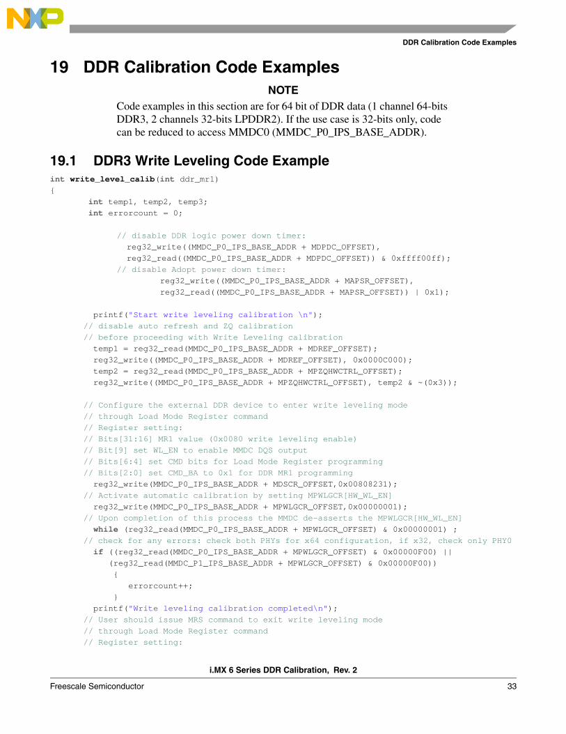
19 DDR Calibration Code ExamplesNOTE
Code examples in this section are for 64 bit of DDR data (1 channel 64-bits DDR3, 2 channels 32-bits LPDDR2). If the use case is 32-bits only, code can be reduced to access MMDC0 (MMDC_P0_IPS_BASE_ADDR).
19.1 DDR3 Write Leveling Code Exampleint write_level_calib(int ddr_mr1) {
int temp1, temp2, temp3; int errorcount = 0;
// disable DDR logic power down timer: reg32_write((MMDC_P0_IPS_BASE_ADDR + MDPDC_OFFSET), reg32_read((MMDC_P0_IPS_BASE_ADDR + MDPDC_OFFSET)) & 0xffff00ff);// disable Adopt power down timer:
reg32_write((MMDC_P0_IPS_BASE_ADDR + MAPSR_OFFSET), reg32_read((MMDC_P0_IPS_BASE_ADDR + MAPSR_OFFSET)) | 0x1);
printf("Start write leveling calibration \n"); // disable auto refresh and ZQ calibration // before proceeding with Write Leveling calibration temp1 = reg32_read(MMDC_P0_IPS_BASE_ADDR + MDREF_OFFSET); reg32_write((MMDC_P0_IPS_BASE_ADDR + MDREF_OFFSET), 0x0000C000); temp2 = reg32_read(MMDC_P0_IPS_BASE_ADDR + MPZQHWCTRL_OFFSET); reg32_write((MMDC_P0_IPS_BASE_ADDR + MPZQHWCTRL_OFFSET), temp2 & ~(0x3));
// Configure the external DDR device to enter write leveling mode // through Load Mode Register command // Register setting: // Bits[31:16] MR1 value (0x0080 write leveling enable) // Bit[9] set WL_EN to enable MMDC DQS output // Bits[6:4] set CMD bits for Load Mode Register programming // Bits[2:0] set CMD_BA to 0x1 for DDR MR1 programming reg32_write(MMDC_P0_IPS_BASE_ADDR + MDSCR_OFFSET,0x00808231); // Activate automatic calibration by setting MPWLGCR[HW_WL_EN] reg32_write(MMDC_P0_IPS_BASE_ADDR + MPWLGCR_OFFSET,0x00000001); // Upon completion of this process the MMDC de-asserts the MPWLGCR[HW_WL_EN] while (reg32_read(MMDC_P0_IPS_BASE_ADDR + MPWLGCR_OFFSET) & 0x00000001) ; // check for any errors: check both PHYs for x64 configuration, if x32, check only PHY0 if ((reg32_read(MMDC_P0_IPS_BASE_ADDR + MPWLGCR_OFFSET) & 0x00000F00) || (reg32_read(MMDC_P1_IPS_BASE_ADDR + MPWLGCR_OFFSET) & 0x00000F00)) { errorcount++; } printf("Write leveling calibration completed\n"); // User should issue MRS command to exit write leveling mode // through Load Mode Register command // Register setting:
i.MX 6 Series DDR Calibration, Rev. 2
34 Freescale Semiconductor
DDR Calibration Code Examples
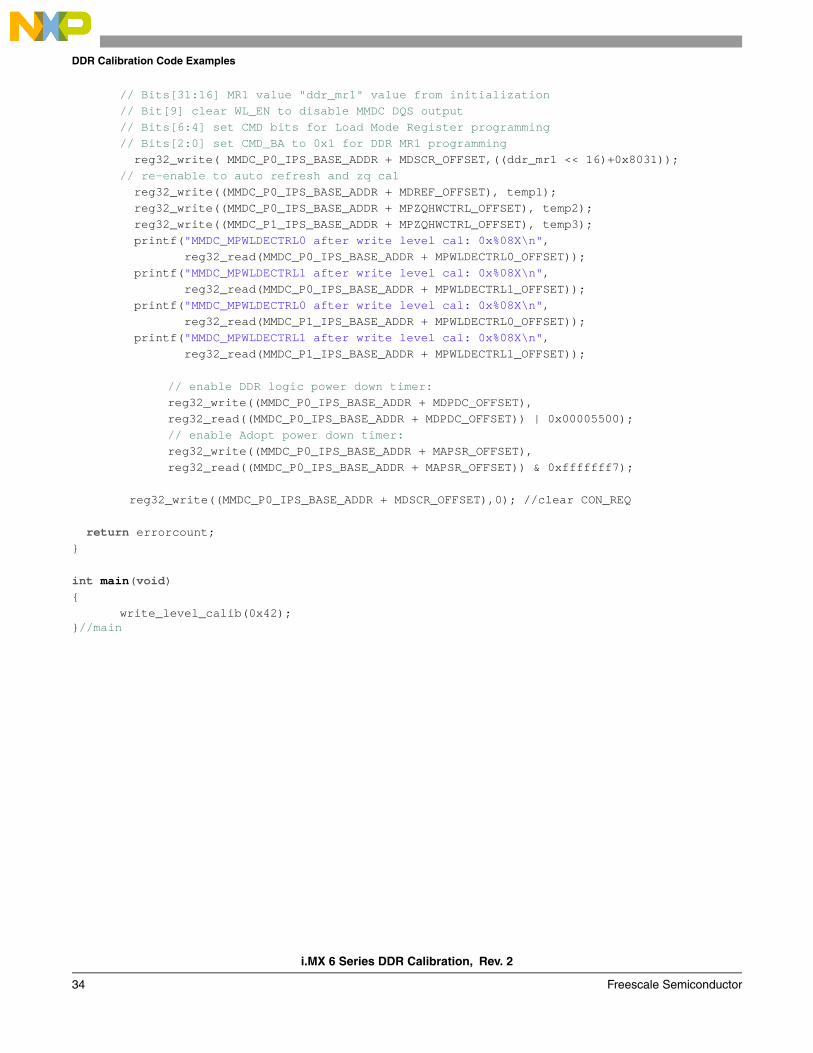
// Bits[31:16] MR1 value "ddr_mr1" value from initialization // Bit[9] clear WL_EN to disable MMDC DQS output // Bits[6:4] set CMD bits for Load Mode Register programming // Bits[2:0] set CMD_BA to 0x1 for DDR MR1 programming reg32_write( MMDC_P0_IPS_BASE_ADDR + MDSCR_OFFSET,((ddr_mr1 << 16)+0x8031)); // re-enable to auto refresh and zq cal reg32_write((MMDC_P0_IPS_BASE_ADDR + MDREF_OFFSET), temp1); reg32_write((MMDC_P0_IPS_BASE_ADDR + MPZQHWCTRL_OFFSET), temp2); reg32_write((MMDC_P1_IPS_BASE_ADDR + MPZQHWCTRL_OFFSET), temp3); printf("MMDC_MPWLDECTRL0 after write level cal: 0x%08X\n", reg32_read(MMDC_P0_IPS_BASE_ADDR + MPWLDECTRL0_OFFSET)); printf("MMDC_MPWLDECTRL1 after write level cal: 0x%08X\n", reg32_read(MMDC_P0_IPS_BASE_ADDR + MPWLDECTRL1_OFFSET)); printf("MMDC_MPWLDECTRL0 after write level cal: 0x%08X\n", reg32_read(MMDC_P1_IPS_BASE_ADDR + MPWLDECTRL0_OFFSET)); printf("MMDC_MPWLDECTRL1 after write level cal: 0x%08X\n", reg32_read(MMDC_P1_IPS_BASE_ADDR + MPWLDECTRL1_OFFSET));
// enable DDR logic power down timer:reg32_write((MMDC_P0_IPS_BASE_ADDR + MDPDC_OFFSET), reg32_read((MMDC_P0_IPS_BASE_ADDR + MDPDC_OFFSET)) | 0x00005500);// enable Adopt power down timer:reg32_write((MMDC_P0_IPS_BASE_ADDR + MAPSR_OFFSET), reg32_read((MMDC_P0_IPS_BASE_ADDR + MAPSR_OFFSET)) & 0xfffffff7);
reg32_write((MMDC_P0_IPS_BASE_ADDR + MDSCR_OFFSET),0); //clear CON_REQ
return errorcount; }
int main(void){
write_level_calib(0x42);}//main
i.MX 6 Series DDR Calibration, Rev. 2
Freescale Semiconductor 35
DDR Calibration Code Examples
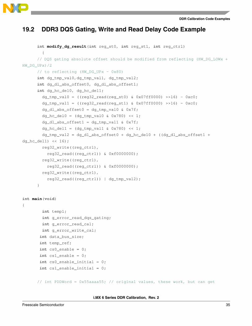
19.2 DDR3 DQS Gating, Write and Read Delay Code Example
int modify_dg_result(int reg_st0, int reg_st1, int reg_ctrl)
{
// DQS gating absolute offset should be modified from reflecting (HW_DG_LOWx +
HW_DG_UPx)/2
// to reflecting (HW_DG_UPx - 0x80)
int dg_tmp_val0,dg_tmp_val1, dg_tmp_val2;
int dg_dl_abs_offset0, dg_dl_abs_offset1;
int dg_hc_del0, dg_hc_del1;
dg_tmp_val0 = ((reg32_read(reg_st0) & 0x07ff0000) >>16) - 0xc0;
dg_tmp_val1 = ((reg32_read(reg_st1) & 0x07ff0000) >>16) - 0xc0;
dg_dl_abs_offset0 = dg_tmp_val0 & 0x7f;
dg_hc_del0 = (dg_tmp_val0 & 0x780) << 1;
dg_dl_abs_offset1 = dg_tmp_val1 & 0x7f;
dg_hc_del1 = (dg_tmp_val1 & 0x780) << 1;
dg_tmp_val2 = dg_dl_abs_offset0 + dg_hc_del0 + ((dg_dl_abs_offset1 +
dg_hc_del1) << 16);
reg32_write((reg_ctrl),
reg32_read((reg_ctrl)) & 0xf0000000);
reg32_write((reg_ctrl),
reg32_read((reg_ctrl)) & 0xf0000000);
reg32_write((reg_ctrl),
reg32_read((reg_ctrl)) | dg_tmp_val2);
}
int main(void)
{
int temp1;
int g_error_read_dqs_gating;
int g_error_read_cal;
int g_error_write_cal;
int data_bus_size;
int temp_ref;
int cs0_enable = 0;
int cs1_enable = 0;
int cs0_enable_initial = 0;
int cs1_enable_initial = 0;
// int PDDWord = 0x55aaaa55; // original values, these work, but can get
i.MX 6 Series DDR Calibration, Rev. 2
36 Freescale Semiconductor
DDR Calibration Code Examples
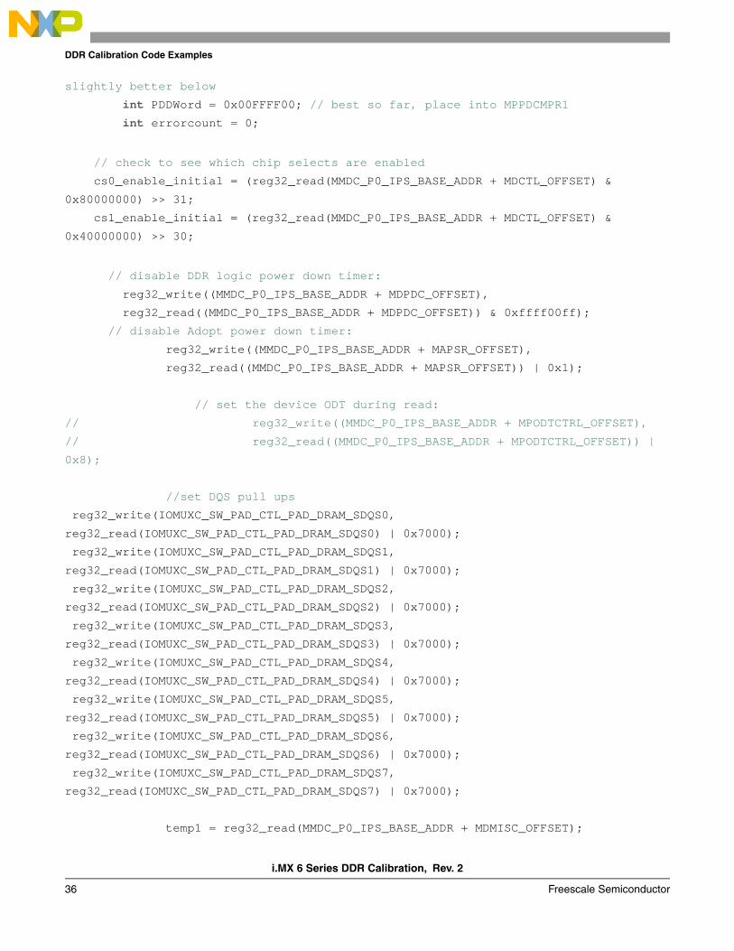
slightly better below
int PDDWord = 0x00FFFF00; // best so far, place into MPPDCMPR1
int errorcount = 0;
// check to see which chip selects are enabled
cs0_enable_initial = (reg32_read(MMDC_P0_IPS_BASE_ADDR + MDCTL_OFFSET) &
0x80000000) >> 31;
cs1_enable_initial = (reg32_read(MMDC_P0_IPS_BASE_ADDR + MDCTL_OFFSET) &
0x40000000) >> 30;
// disable DDR logic power down timer:
reg32_write((MMDC_P0_IPS_BASE_ADDR + MDPDC_OFFSET),
reg32_read((MMDC_P0_IPS_BASE_ADDR + MDPDC_OFFSET)) & 0xffff00ff);
// disable Adopt power down timer:
reg32_write((MMDC_P0_IPS_BASE_ADDR + MAPSR_OFFSET),
reg32_read((MMDC_P0_IPS_BASE_ADDR + MAPSR_OFFSET)) | 0x1);
// set the device ODT during read:
// reg32_write((MMDC_P0_IPS_BASE_ADDR + MPODTCTRL_OFFSET),
// reg32_read((MMDC_P0_IPS_BASE_ADDR + MPODTCTRL_OFFSET)) |
0x8);
//set DQS pull ups
reg32_write(IOMUXC_SW_PAD_CTL_PAD_DRAM_SDQS0,
reg32_read(IOMUXC_SW_PAD_CTL_PAD_DRAM_SDQS0) | 0x7000);
reg32_write(IOMUXC_SW_PAD_CTL_PAD_DRAM_SDQS1,
reg32_read(IOMUXC_SW_PAD_CTL_PAD_DRAM_SDQS1) | 0x7000);
reg32_write(IOMUXC_SW_PAD_CTL_PAD_DRAM_SDQS2,
reg32_read(IOMUXC_SW_PAD_CTL_PAD_DRAM_SDQS2) | 0x7000);
reg32_write(IOMUXC_SW_PAD_CTL_PAD_DRAM_SDQS3,
reg32_read(IOMUXC_SW_PAD_CTL_PAD_DRAM_SDQS3) | 0x7000);
reg32_write(IOMUXC_SW_PAD_CTL_PAD_DRAM_SDQS4,
reg32_read(IOMUXC_SW_PAD_CTL_PAD_DRAM_SDQS4) | 0x7000);
reg32_write(IOMUXC_SW_PAD_CTL_PAD_DRAM_SDQS5,
reg32_read(IOMUXC_SW_PAD_CTL_PAD_DRAM_SDQS5) | 0x7000);
reg32_write(IOMUXC_SW_PAD_CTL_PAD_DRAM_SDQS6,
reg32_read(IOMUXC_SW_PAD_CTL_PAD_DRAM_SDQS6) | 0x7000);
reg32_write(IOMUXC_SW_PAD_CTL_PAD_DRAM_SDQS7,
reg32_read(IOMUXC_SW_PAD_CTL_PAD_DRAM_SDQS7) | 0x7000);
temp1 = reg32_read(MMDC_P0_IPS_BASE_ADDR + MDMISC_OFFSET);
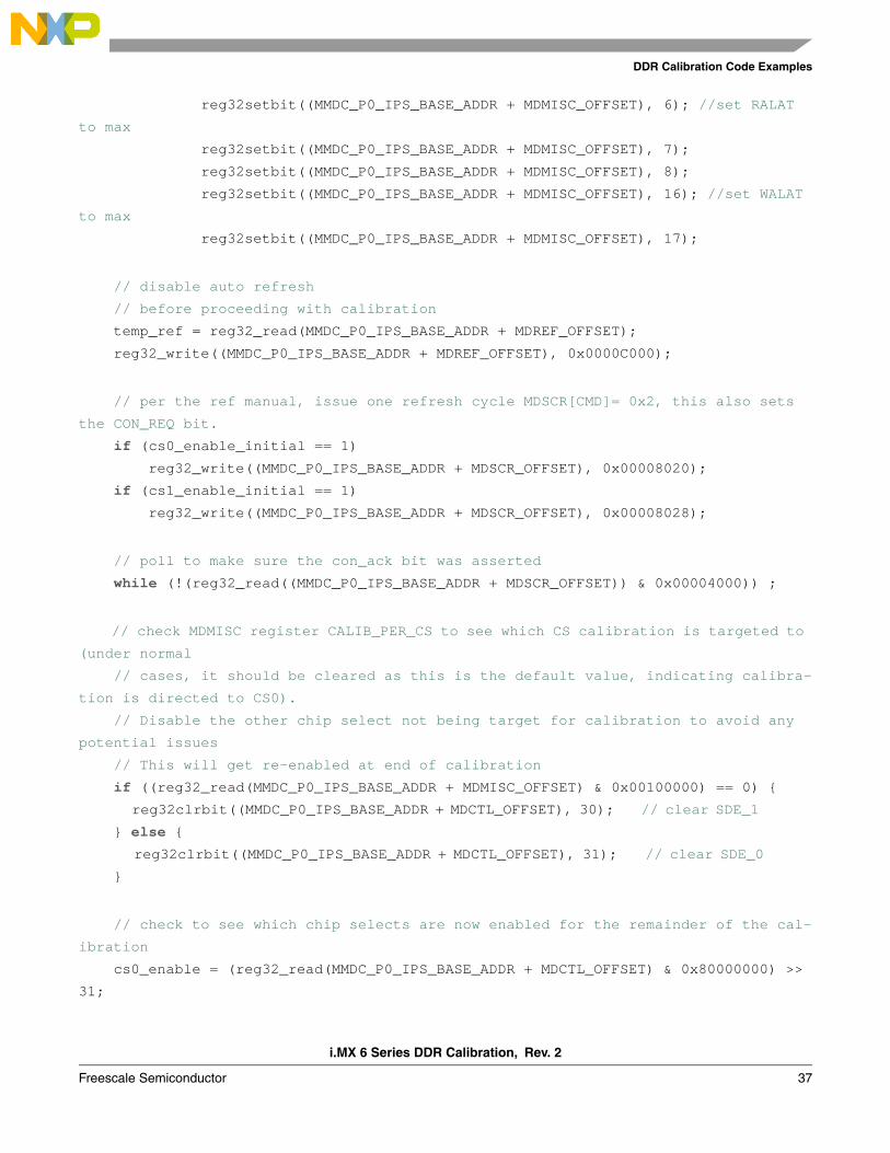
i.MX 6 Series DDR Calibration, Rev. 2
Freescale Semiconductor 37
DDR Calibration Code Examples
reg32setbit((MMDC_P0_IPS_BASE_ADDR + MDMISC_OFFSET), 6); //set RALAT
to max
reg32setbit((MMDC_P0_IPS_BASE_ADDR + MDMISC_OFFSET), 7);
reg32setbit((MMDC_P0_IPS_BASE_ADDR + MDMISC_OFFSET), 8);
reg32setbit((MMDC_P0_IPS_BASE_ADDR + MDMISC_OFFSET), 16); //set WALAT
to max
reg32setbit((MMDC_P0_IPS_BASE_ADDR + MDMISC_OFFSET), 17);
// disable auto refresh
// before proceeding with calibration
temp_ref = reg32_read(MMDC_P0_IPS_BASE_ADDR + MDREF_OFFSET);
reg32_write((MMDC_P0_IPS_BASE_ADDR + MDREF_OFFSET), 0x0000C000);
// per the ref manual, issue one refresh cycle MDSCR[CMD]= 0x2, this also sets
the CON_REQ bit.
if (cs0_enable_initial == 1)
reg32_write((MMDC_P0_IPS_BASE_ADDR + MDSCR_OFFSET), 0x00008020);
if (cs1_enable_initial == 1)
reg32_write((MMDC_P0_IPS_BASE_ADDR + MDSCR_OFFSET), 0x00008028);
// poll to make sure the con_ack bit was asserted
while (!(reg32_read((MMDC_P0_IPS_BASE_ADDR + MDSCR_OFFSET)) & 0x00004000)) ;
// check MDMISC register CALIB_PER_CS to see which CS calibration is targeted to
(under normal
// cases, it should be cleared as this is the default value, indicating calibra-
tion is directed to CS0).
// Disable the other chip select not being target for calibration to avoid any
potential issues
// This will get re-enabled at end of calibration
if ((reg32_read(MMDC_P0_IPS_BASE_ADDR + MDMISC_OFFSET) & 0x00100000) == 0) {
reg32clrbit((MMDC_P0_IPS_BASE_ADDR + MDCTL_OFFSET), 30); // clear SDE_1
} else {
reg32clrbit((MMDC_P0_IPS_BASE_ADDR + MDCTL_OFFSET), 31); // clear SDE_0
}
// check to see which chip selects are now enabled for the remainder of the cal-
ibration
cs0_enable = (reg32_read(MMDC_P0_IPS_BASE_ADDR + MDCTL_OFFSET) & 0x80000000) >>
31;
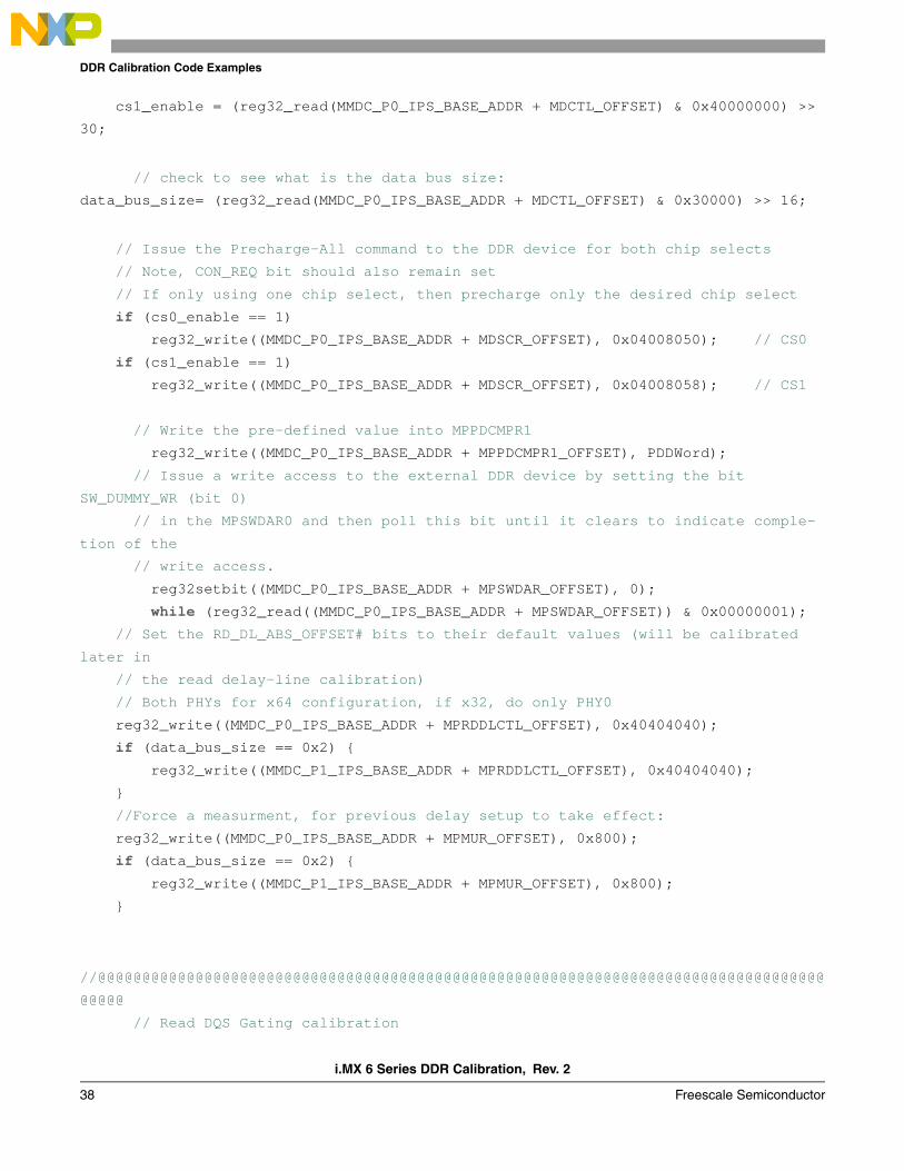
i.MX 6 Series DDR Calibration, Rev. 2
38 Freescale Semiconductor
DDR Calibration Code Examples
cs1_enable = (reg32_read(MMDC_P0_IPS_BASE_ADDR + MDCTL_OFFSET) & 0x40000000) >>
30;
// check to see what is the data bus size:
data_bus_size= (reg32_read(MMDC_P0_IPS_BASE_ADDR + MDCTL_OFFSET) & 0x30000) >> 16;
// Issue the Precharge-All command to the DDR device for both chip selects
// Note, CON_REQ bit should also remain set
// If only using one chip select, then precharge only the desired chip select
if (cs0_enable == 1)
reg32_write((MMDC_P0_IPS_BASE_ADDR + MDSCR_OFFSET), 0x04008050); // CS0
if (cs1_enable == 1)
reg32_write((MMDC_P0_IPS_BASE_ADDR + MDSCR_OFFSET), 0x04008058); // CS1
// Write the pre-defined value into MPPDCMPR1
reg32_write((MMDC_P0_IPS_BASE_ADDR + MPPDCMPR1_OFFSET), PDDWord);
// Issue a write access to the external DDR device by setting the bit
SW_DUMMY_WR (bit 0)
// in the MPSWDAR0 and then poll this bit until it clears to indicate comple-
tion of the
// write access.
reg32setbit((MMDC_P0_IPS_BASE_ADDR + MPSWDAR_OFFSET), 0);
while (reg32_read((MMDC_P0_IPS_BASE_ADDR + MPSWDAR_OFFSET)) & 0x00000001);
// Set the RD_DL_ABS_OFFSET# bits to their default values (will be calibrated
later in
// the read delay-line calibration)
// Both PHYs for x64 configuration, if x32, do only PHY0
reg32_write((MMDC_P0_IPS_BASE_ADDR + MPRDDLCTL_OFFSET), 0x40404040);
if (data_bus_size == 0x2) {
reg32_write((MMDC_P1_IPS_BASE_ADDR + MPRDDLCTL_OFFSET), 0x40404040);
}
//Force a measurment, for previous delay setup to take effect:
reg32_write((MMDC_P0_IPS_BASE_ADDR + MPMUR_OFFSET), 0x800);
if (data_bus_size == 0x2) {
reg32_write((MMDC_P1_IPS_BASE_ADDR + MPMUR_OFFSET), 0x800);
}
//@@@@@@@@@@@@@@@@@@@@@@@@@@@@@@@@@@@@@@@@@@@@@@@@@@@@@@@@@@@@@@@@@@@@@@@@@@@@@@@@@@
@@@@@
// Read DQS Gating calibration
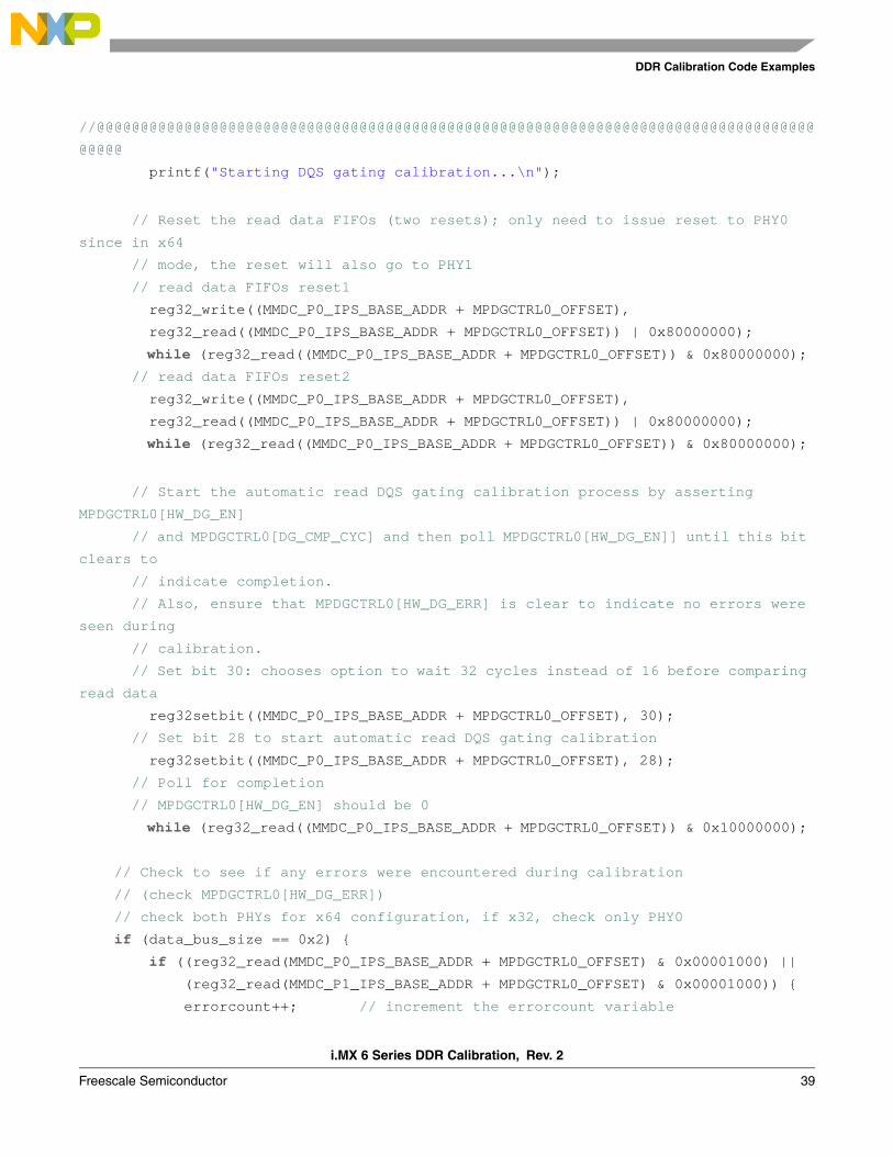
i.MX 6 Series DDR Calibration, Rev. 2
Freescale Semiconductor 39
DDR Calibration Code Examples
//@@@@@@@@@@@@@@@@@@@@@@@@@@@@@@@@@@@@@@@@@@@@@@@@@@@@@@@@@@@@@@@@@@@@@@@@@@@@@@@@@@
@@@@@
printf("Starting DQS gating calibration...\n");
// Reset the read data FIFOs (two resets); only need to issue reset to PHY0
since in x64
// mode, the reset will also go to PHY1
// read data FIFOs reset1
reg32_write((MMDC_P0_IPS_BASE_ADDR + MPDGCTRL0_OFFSET),
reg32_read((MMDC_P0_IPS_BASE_ADDR + MPDGCTRL0_OFFSET)) | 0x80000000);
while (reg32_read((MMDC_P0_IPS_BASE_ADDR + MPDGCTRL0_OFFSET)) & 0x80000000);
// read data FIFOs reset2
reg32_write((MMDC_P0_IPS_BASE_ADDR + MPDGCTRL0_OFFSET),
reg32_read((MMDC_P0_IPS_BASE_ADDR + MPDGCTRL0_OFFSET)) | 0x80000000);
while (reg32_read((MMDC_P0_IPS_BASE_ADDR + MPDGCTRL0_OFFSET)) & 0x80000000);
// Start the automatic read DQS gating calibration process by asserting
MPDGCTRL0[HW_DG_EN]
// and MPDGCTRL0[DG_CMP_CYC] and then poll MPDGCTRL0[HW_DG_EN]] until this bit
clears to
// indicate completion.
// Also, ensure that MPDGCTRL0[HW_DG_ERR] is clear to indicate no errors were
seen during
// calibration.
// Set bit 30: chooses option to wait 32 cycles instead of 16 before comparing
read data
reg32setbit((MMDC_P0_IPS_BASE_ADDR + MPDGCTRL0_OFFSET), 30);
// Set bit 28 to start automatic read DQS gating calibration
reg32setbit((MMDC_P0_IPS_BASE_ADDR + MPDGCTRL0_OFFSET), 28);
// Poll for completion
// MPDGCTRL0[HW_DG_EN] should be 0
while (reg32_read((MMDC_P0_IPS_BASE_ADDR + MPDGCTRL0_OFFSET)) & 0x10000000);
// Check to see if any errors were encountered during calibration
// (check MPDGCTRL0[HW_DG_ERR])
// check both PHYs for x64 configuration, if x32, check only PHY0
if (data_bus_size == 0x2) {
if ((reg32_read(MMDC_P0_IPS_BASE_ADDR + MPDGCTRL0_OFFSET) & 0x00001000) ||
(reg32_read(MMDC_P1_IPS_BASE_ADDR + MPDGCTRL0_OFFSET) & 0x00001000)) {
errorcount++; // increment the errorcount variable
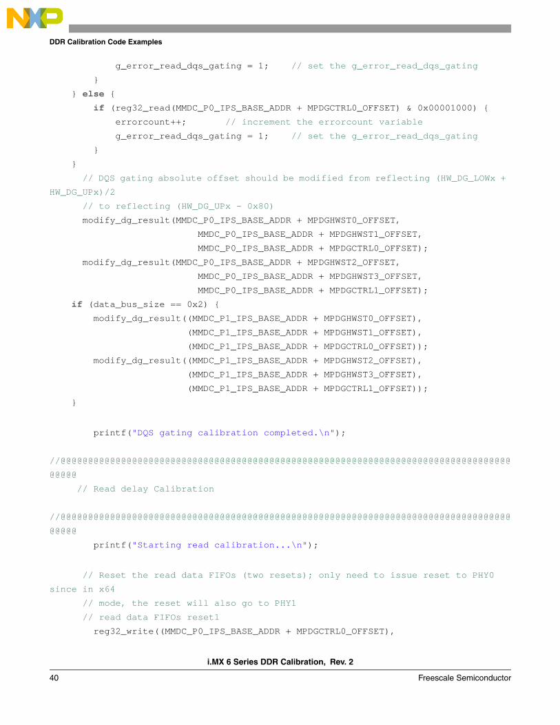
i.MX 6 Series DDR Calibration, Rev. 2
40 Freescale Semiconductor
DDR Calibration Code Examples
g_error_read_dqs_gating = 1; // set the g_error_read_dqs_gating
}
} else {
if (reg32_read(MMDC_P0_IPS_BASE_ADDR + MPDGCTRL0_OFFSET) & 0x00001000) {
errorcount++; // increment the errorcount variable
g_error_read_dqs_gating = 1; // set the g_error_read_dqs_gating
}
}
// DQS gating absolute offset should be modified from reflecting (HW_DG_LOWx +
HW_DG_UPx)/2
// to reflecting (HW_DG_UPx - 0x80)
modify_dg_result(MMDC_P0_IPS_BASE_ADDR + MPDGHWST0_OFFSET,
MMDC_P0_IPS_BASE_ADDR + MPDGHWST1_OFFSET,
MMDC_P0_IPS_BASE_ADDR + MPDGCTRL0_OFFSET);
modify_dg_result(MMDC_P0_IPS_BASE_ADDR + MPDGHWST2_OFFSET,
MMDC_P0_IPS_BASE_ADDR + MPDGHWST3_OFFSET,
MMDC_P0_IPS_BASE_ADDR + MPDGCTRL1_OFFSET);
if (data_bus_size == 0x2) {
modify_dg_result((MMDC_P1_IPS_BASE_ADDR + MPDGHWST0_OFFSET),
(MMDC_P1_IPS_BASE_ADDR + MPDGHWST1_OFFSET),
(MMDC_P1_IPS_BASE_ADDR + MPDGCTRL0_OFFSET));
modify_dg_result((MMDC_P1_IPS_BASE_ADDR + MPDGHWST2_OFFSET),
(MMDC_P1_IPS_BASE_ADDR + MPDGHWST3_OFFSET),
(MMDC_P1_IPS_BASE_ADDR + MPDGCTRL1_OFFSET));
}
printf("DQS gating calibration completed.\n");
//@@@@@@@@@@@@@@@@@@@@@@@@@@@@@@@@@@@@@@@@@@@@@@@@@@@@@@@@@@@@@@@@@@@@@@@@@@@@@@@@@@
@@@@@
// Read delay Calibration
//@@@@@@@@@@@@@@@@@@@@@@@@@@@@@@@@@@@@@@@@@@@@@@@@@@@@@@@@@@@@@@@@@@@@@@@@@@@@@@@@@@
@@@@@
printf("Starting read calibration...\n");
// Reset the read data FIFOs (two resets); only need to issue reset to PHY0
since in x64
// mode, the reset will also go to PHY1
// read data FIFOs reset1
reg32_write((MMDC_P0_IPS_BASE_ADDR + MPDGCTRL0_OFFSET),
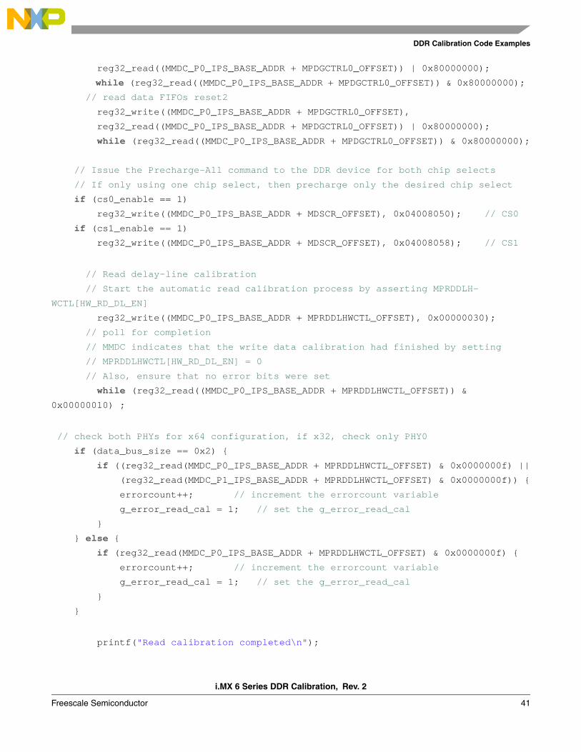
i.MX 6 Series DDR Calibration, Rev. 2
Freescale Semiconductor 41
DDR Calibration Code Examples
reg32_read((MMDC_P0_IPS_BASE_ADDR + MPDGCTRL0_OFFSET)) | 0x80000000);
while (reg32_read((MMDC_P0_IPS_BASE_ADDR + MPDGCTRL0_OFFSET)) & 0x80000000);
// read data FIFOs reset2
reg32_write((MMDC_P0_IPS_BASE_ADDR + MPDGCTRL0_OFFSET),
reg32_read((MMDC_P0_IPS_BASE_ADDR + MPDGCTRL0_OFFSET)) | 0x80000000);
while (reg32_read((MMDC_P0_IPS_BASE_ADDR + MPDGCTRL0_OFFSET)) & 0x80000000);
// Issue the Precharge-All command to the DDR device for both chip selects
// If only using one chip select, then precharge only the desired chip select
if (cs0_enable == 1)
reg32_write((MMDC_P0_IPS_BASE_ADDR + MDSCR_OFFSET), 0x04008050); // CS0
if (cs1_enable == 1)
reg32_write((MMDC_P0_IPS_BASE_ADDR + MDSCR_OFFSET), 0x04008058); // CS1
// Read delay-line calibration
// Start the automatic read calibration process by asserting MPRDDLH-
WCTL[HW_RD_DL_EN]
reg32_write((MMDC_P0_IPS_BASE_ADDR + MPRDDLHWCTL_OFFSET), 0x00000030);
// poll for completion
// MMDC indicates that the write data calibration had finished by setting
// MPRDDLHWCTL[HW_RD_DL_EN] = 0
// Also, ensure that no error bits were set
while (reg32_read((MMDC_P0_IPS_BASE_ADDR + MPRDDLHWCTL_OFFSET)) &
0x00000010) ;
// check both PHYs for x64 configuration, if x32, check only PHY0
if (data_bus_size == 0x2) {
if ((reg32_read(MMDC_P0_IPS_BASE_ADDR + MPRDDLHWCTL_OFFSET) & 0x0000000f) ||
(reg32_read(MMDC_P1_IPS_BASE_ADDR + MPRDDLHWCTL_OFFSET) & 0x0000000f)) {
errorcount++; // increment the errorcount variable
g_error_read_cal = 1; // set the g_error_read_cal
}
} else {
if (reg32_read(MMDC_P0_IPS_BASE_ADDR + MPRDDLHWCTL_OFFSET) & 0x0000000f) {
errorcount++; // increment the errorcount variable
g_error_read_cal = 1; // set the g_error_read_cal
}
}
printf("Read calibration completed\n");
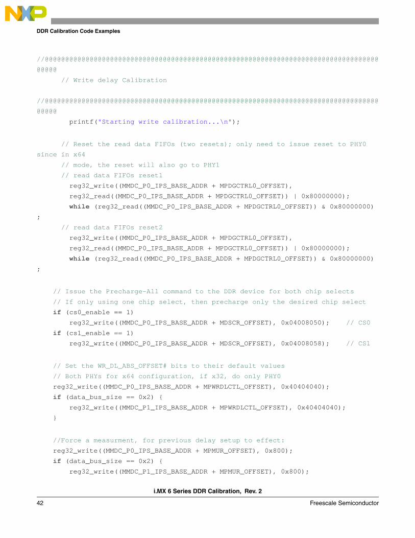
i.MX 6 Series DDR Calibration, Rev. 2
42 Freescale Semiconductor
DDR Calibration Code Examples
//@@@@@@@@@@@@@@@@@@@@@@@@@@@@@@@@@@@@@@@@@@@@@@@@@@@@@@@@@@@@@@@@@@@@@@@@@@@@@@@@@@
@@@@@
// Write delay Calibration
//@@@@@@@@@@@@@@@@@@@@@@@@@@@@@@@@@@@@@@@@@@@@@@@@@@@@@@@@@@@@@@@@@@@@@@@@@@@@@@@@@@
@@@@@
printf("Starting write calibration...\n");
// Reset the read data FIFOs (two resets); only need to issue reset to PHY0
since in x64
// mode, the reset will also go to PHY1
// read data FIFOs reset1
reg32_write((MMDC_P0_IPS_BASE_ADDR + MPDGCTRL0_OFFSET),
reg32_read((MMDC_P0_IPS_BASE_ADDR + MPDGCTRL0_OFFSET)) | 0x80000000);
while (reg32_read((MMDC_P0_IPS_BASE_ADDR + MPDGCTRL0_OFFSET)) & 0x80000000)
;
// read data FIFOs reset2
reg32_write((MMDC_P0_IPS_BASE_ADDR + MPDGCTRL0_OFFSET),
reg32_read((MMDC_P0_IPS_BASE_ADDR + MPDGCTRL0_OFFSET)) | 0x80000000);
while (reg32_read((MMDC_P0_IPS_BASE_ADDR + MPDGCTRL0_OFFSET)) & 0x80000000)
;
// Issue the Precharge-All command to the DDR device for both chip selects
// If only using one chip select, then precharge only the desired chip select
if (cs0_enable == 1)
reg32_write((MMDC_P0_IPS_BASE_ADDR + MDSCR_OFFSET), 0x04008050); // CS0
if (cs1_enable == 1)
reg32_write((MMDC_P0_IPS_BASE_ADDR + MDSCR_OFFSET), 0x04008058); // CS1
// Set the WR_DL_ABS_OFFSET# bits to their default values
// Both PHYs for x64 configuration, if x32, do only PHY0
reg32_write((MMDC_P0_IPS_BASE_ADDR + MPWRDLCTL_OFFSET), 0x40404040);
if (data_bus_size == 0x2) {
reg32_write((MMDC_P1_IPS_BASE_ADDR + MPWRDLCTL_OFFSET), 0x40404040);
}
//Force a measurment, for previous delay setup to effect:
reg32_write((MMDC_P0_IPS_BASE_ADDR + MPMUR_OFFSET), 0x800);
if (data_bus_size == 0x2) {
reg32_write((MMDC_P1_IPS_BASE_ADDR + MPMUR_OFFSET), 0x800);
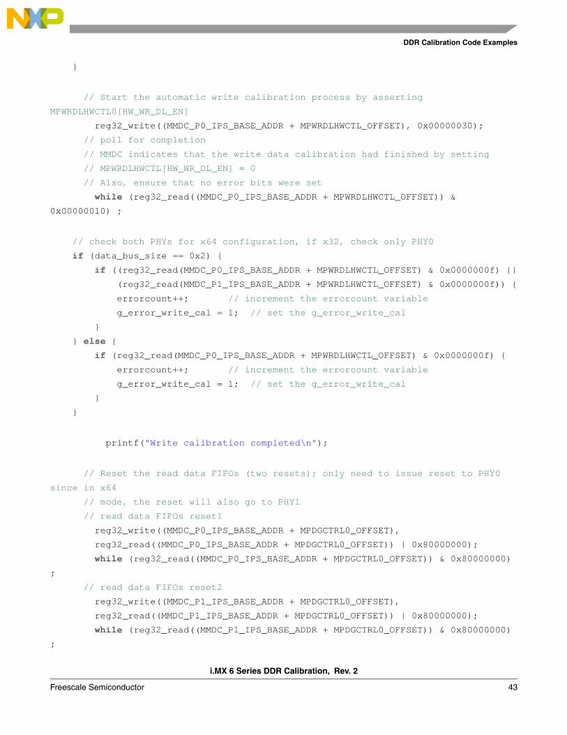
i.MX 6 Series DDR Calibration, Rev. 2
Freescale Semiconductor 43
DDR Calibration Code Examples
}
// Start the automatic write calibration process by asserting
MPWRDLHWCTL0[HW_WR_DL_EN]
reg32_write((MMDC_P0_IPS_BASE_ADDR + MPWRDLHWCTL_OFFSET), 0x00000030);
// poll for completion
// MMDC indicates that the write data calibration had finished by setting
// MPWRDLHWCTL[HW_WR_DL_EN] = 0
// Also, ensure that no error bits were set
while (reg32_read((MMDC_P0_IPS_BASE_ADDR + MPWRDLHWCTL_OFFSET)) &
0x00000010) ;
// check both PHYs for x64 configuration, if x32, check only PHY0
if (data_bus_size == 0x2) {
if ((reg32_read(MMDC_P0_IPS_BASE_ADDR + MPWRDLHWCTL_OFFSET) & 0x0000000f) ||
(reg32_read(MMDC_P1_IPS_BASE_ADDR + MPWRDLHWCTL_OFFSET) & 0x0000000f)) {
errorcount++; // increment the errorcount variable
g_error_write_cal = 1; // set the g_error_write_cal
}
} else {
if (reg32_read(MMDC_P0_IPS_BASE_ADDR + MPWRDLHWCTL_OFFSET) & 0x0000000f) {
errorcount++; // increment the errorcount variable
g_error_write_cal = 1; // set the g_error_write_cal
}
}
printf("Write calibration completed\n");
// Reset the read data FIFOs (two resets); only need to issue reset to PHY0
since in x64
// mode, the reset will also go to PHY1
// read data FIFOs reset1
reg32_write((MMDC_P0_IPS_BASE_ADDR + MPDGCTRL0_OFFSET),
reg32_read((MMDC_P0_IPS_BASE_ADDR + MPDGCTRL0_OFFSET)) | 0x80000000);
while (reg32_read((MMDC_P0_IPS_BASE_ADDR + MPDGCTRL0_OFFSET)) & 0x80000000)
;
// read data FIFOs reset2
reg32_write((MMDC_P1_IPS_BASE_ADDR + MPDGCTRL0_OFFSET),
reg32_read((MMDC_P1_IPS_BASE_ADDR + MPDGCTRL0_OFFSET)) | 0x80000000);
while (reg32_read((MMDC_P1_IPS_BASE_ADDR + MPDGCTRL0_OFFSET)) & 0x80000000)
;
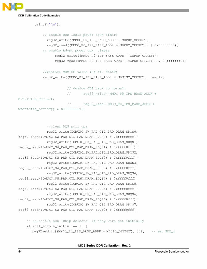
i.MX 6 Series DDR Calibration, Rev. 2
44 Freescale Semiconductor
DDR Calibration Code Examples
printf("\n");
// enable DDR logic power down timer:
reg32_write((MMDC_P0_IPS_BASE_ADDR + MDPDC_OFFSET),
reg32_read((MMDC_P0_IPS_BASE_ADDR + MDPDC_OFFSET)) | 0x00005500);
// enable Adopt power down timer:
reg32_write((MMDC_P0_IPS_BASE_ADDR + MAPSR_OFFSET),
reg32_read((MMDC_P0_IPS_BASE_ADDR + MAPSR_OFFSET)) & 0xfffffff7);
//restore MDMISC value (RALAT, WALAT)
reg32_write((MMDC_P1_IPS_BASE_ADDR + MDMISC_OFFSET), temp1);
// device ODT back to normal:
// reg32_write((MMDC_P0_IPS_BASE_ADDR +
MPODTCTRL_OFFSET),
// reg32_read((MMDC_P0_IPS_BASE_ADDR +
MPODTCTRL_OFFSET)) & 0xfffffff7);
//clear DQS pull ups
reg32_write(IOMUXC_SW_PAD_CTL_PAD_DRAM_SDQS0,
reg32_read(IOMUXC_SW_PAD_CTL_PAD_DRAM_SDQS0) & 0xffff0fff);
reg32_write(IOMUXC_SW_PAD_CTL_PAD_DRAM_SDQS1,
reg32_read(IOMUXC_SW_PAD_CTL_PAD_DRAM_SDQS1) & 0xffff0fff);
reg32_write(IOMUXC_SW_PAD_CTL_PAD_DRAM_SDQS2,
reg32_read(IOMUXC_SW_PAD_CTL_PAD_DRAM_SDQS2) & 0xffff0fff);
reg32_write(IOMUXC_SW_PAD_CTL_PAD_DRAM_SDQS3,
reg32_read(IOMUXC_SW_PAD_CTL_PAD_DRAM_SDQS3) & 0xffff0fff);
reg32_write(IOMUXC_SW_PAD_CTL_PAD_DRAM_SDQS4,
reg32_read(IOMUXC_SW_PAD_CTL_PAD_DRAM_SDQS4) & 0xffff0fff);
reg32_write(IOMUXC_SW_PAD_CTL_PAD_DRAM_SDQS5,
reg32_read(IOMUXC_SW_PAD_CTL_PAD_DRAM_SDQS5) & 0xffff0fff);
reg32_write(IOMUXC_SW_PAD_CTL_PAD_DRAM_SDQS6,
reg32_read(IOMUXC_SW_PAD_CTL_PAD_DRAM_SDQS6) & 0xffff0fff);
reg32_write(IOMUXC_SW_PAD_CTL_PAD_DRAM_SDQS7,
reg32_read(IOMUXC_SW_PAD_CTL_PAD_DRAM_SDQS7) & 0xffff0fff);
// re-enable SDE (chip selects) if they were set initially
if (cs1_enable_initial == 1) {
reg32setbit((MMDC_P0_IPS_BASE_ADDR + MDCTL_OFFSET), 30); // set SDE_1
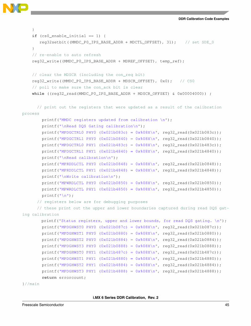
i.MX 6 Series DDR Calibration, Rev. 2
Freescale Semiconductor 45
DDR Calibration Code Examples
}
if (cs0_enable_initial == 1) {
reg32setbit((MMDC_P0_IPS_BASE_ADDR + MDCTL_OFFSET), 31); // set SDE_0
}
// re-enable to auto refresh
reg32_write((MMDC_P0_IPS_BASE_ADDR + MDREF_OFFSET), temp_ref);
// clear the MDSCR (including the con_req bit)
reg32_write((MMDC_P0_IPS_BASE_ADDR + MDSCR_OFFSET), 0x0); // CS0
// poll to make sure the con_ack bit is clear
while ((reg32_read(MMDC_P0_IPS_BASE_ADDR + MDSCR_OFFSET) & 0x00004000)) ;
// print out the registers that were updated as a result of the calibration
process
printf("MMDC registers updated from calibration \n");
printf("\nRead DQS Gating calibration\n");
printf("MPDGCTRL0 PHY0 (0x021b083c) = 0x%08X\n", reg32_read(0x021b083c));
printf("MPDGCTRL1 PHY0 (0x021b0840) = 0x%08X\n", reg32_read(0x021b0840));
printf("MPDGCTRL0 PHY1 (0x021b483c) = 0x%08X\n", reg32_read(0x021b483c));
printf("MPDGCTRL1 PHY1 (0x021b4840) = 0x%08X\n", reg32_read(0x021b4840));
printf("\nRead calibration\n");
printf("MPRDDLCTL PHY0 (0x021b0848) = 0x%08X\n", reg32_read(0x021b0848));
printf("MPRDDLCTL PHY1 (0x021b4848) = 0x%08X\n", reg32_read(0x021b4848));
printf("\nWrite calibration\n");
printf("MPWRDLCTL PHY0 (0x021b0850) = 0x%08X\n", reg32_read(0x021b0850));
printf("MPWRDLCTL PHY1 (0x021b4850) = 0x%08X\n", reg32_read(0x021b4850));
printf("\n");
// registers below are for debugging purposes
// these print out the upper and lower boundaries captured during read DQS gat-
ing calibration
printf("Status registers, upper and lower bounds, for read DQS gating. \n");
printf("MPDGHWST0 PHY0 (0x021b087c) = 0x%08X\n", reg32_read(0x021b087c));
printf("MPDGHWST1 PHY0 (0x021b0880) = 0x%08X\n", reg32_read(0x021b0880));
printf("MPDGHWST2 PHY0 (0x021b0884) = 0x%08X\n", reg32_read(0x021b0884));
printf("MPDGHWST3 PHY0 (0x021b0888) = 0x%08X\n", reg32_read(0x021b0888));
printf("MPDGHWST0 PHY1 (0x021b487c) = 0x%08X\n", reg32_read(0x021b487c));
printf("MPDGHWST1 PHY1 (0x021b4880) = 0x%08X\n", reg32_read(0x021b4880));
printf("MPDGHWST2 PHY1 (0x021b4884) = 0x%08X\n", reg32_read(0x021b4884));
printf("MPDGHWST3 PHY1 (0x021b4888) = 0x%08X\n", reg32_read(0x021b4888));
return errorcount;
}//main
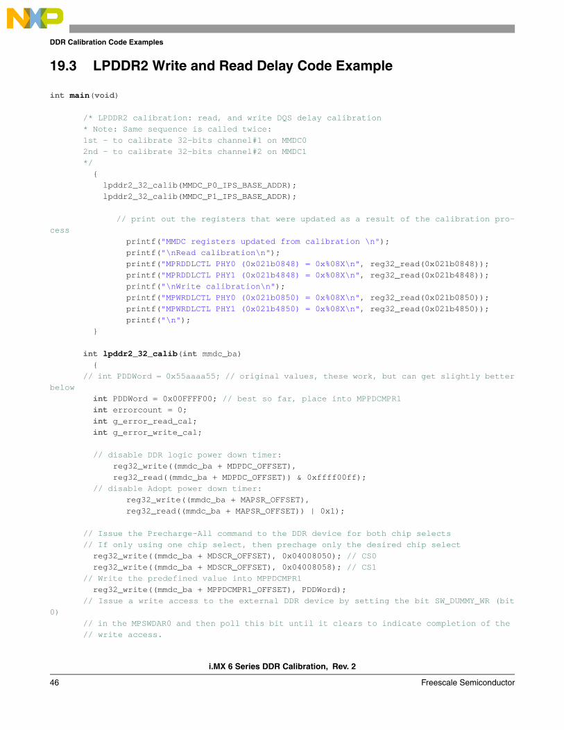
i.MX 6 Series DDR Calibration, Rev. 2
46 Freescale Semiconductor
DDR Calibration Code Examples
19.3 LPDDR2 Write and Read Delay Code Example
int main(void)
/* LPDDR2 calibration: read, and write DQS delay calibration * Note: Same sequence is called twice:1st - to calibrate 32-bits channel#1 on MMDC02nd - to calibrate 32-bits channel#2 on MMDC1*/ { lpddr2_32_calib(MMDC_P0_IPS_BASE_ADDR); lpddr2_32_calib(MMDC_P1_IPS_BASE_ADDR);
// print out the registers that were updated as a result of the calibration pro-cess
printf("MMDC registers updated from calibration \n"); printf("\nRead calibration\n"); printf("MPRDDLCTL PHY0 (0x021b0848) = 0x%08X\n", reg32_read(0x021b0848)); printf("MPRDDLCTL PHY1 (0x021b4848) = 0x%08X\n", reg32_read(0x021b4848)); printf("\nWrite calibration\n"); printf("MPWRDLCTL PHY0 (0x021b0850) = 0x%08X\n", reg32_read(0x021b0850)); printf("MPWRDLCTL PHY1 (0x021b4850) = 0x%08X\n", reg32_read(0x021b4850)); printf("\n");
}
int lpddr2_32_calib(int mmdc_ba) { // int PDDWord = 0x55aaaa55; // original values, these work, but can get slightly better
below int PDDWord = 0x00FFFF00; // best so far, place into MPPDCMPR1 int errorcount = 0; int g_error_read_cal; int g_error_write_cal;
// disable DDR logic power down timer: reg32_write((mmdc_ba + MDPDC_OFFSET), reg32_read((mmdc_ba + MDPDC_OFFSET)) & 0xffff00ff); // disable Adopt power down timer:
reg32_write((mmdc_ba + MAPSR_OFFSET), reg32_read((mmdc_ba + MAPSR_OFFSET)) | 0x1);
// Issue the Precharge-All command to the DDR device for both chip selects // If only using one chip select, then prechage only the desired chip select reg32_write((mmdc_ba + MDSCR_OFFSET), 0x04008050); // CS0 reg32_write((mmdc_ba + MDSCR_OFFSET), 0x04008058); // CS1 // Write the predefined value into MPPDCMPR1 reg32_write((mmdc_ba + MPPDCMPR1_OFFSET), PDDWord); // Issue a write access to the external DDR device by setting the bit SW_DUMMY_WR (bit
0) // in the MPSWDAR0 and then poll this bit until it clears to indicate completion of the // write access.
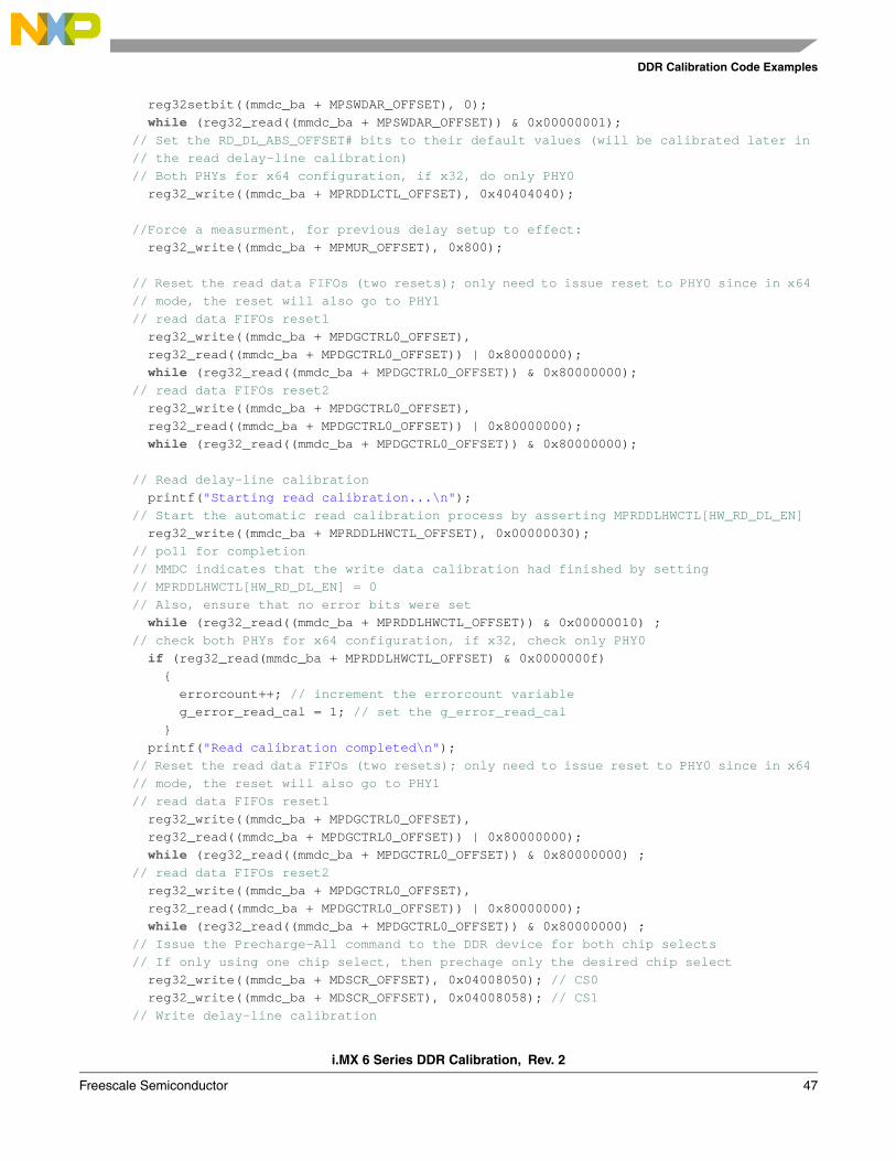
i.MX 6 Series DDR Calibration, Rev. 2
Freescale Semiconductor 47
DDR Calibration Code Examples
reg32setbit((mmdc_ba + MPSWDAR_OFFSET), 0); while (reg32_read((mmdc_ba + MPSWDAR_OFFSET)) & 0x00000001); // Set the RD_DL_ABS_OFFSET# bits to their default values (will be calibrated later in // the read delay-line calibration) // Both PHYs for x64 configuration, if x32, do only PHY0 reg32_write((mmdc_ba + MPRDDLCTL_OFFSET), 0x40404040);
//Force a measurment, for previous delay setup to effect: reg32_write((mmdc_ba + MPMUR_OFFSET), 0x800);
// Reset the read data FIFOs (two resets); only need to issue reset to PHY0 since in x64 // mode, the reset will also go to PHY1 // read data FIFOs reset1 reg32_write((mmdc_ba + MPDGCTRL0_OFFSET), reg32_read((mmdc_ba + MPDGCTRL0_OFFSET)) | 0x80000000); while (reg32_read((mmdc_ba + MPDGCTRL0_OFFSET)) & 0x80000000); // read data FIFOs reset2 reg32_write((mmdc_ba + MPDGCTRL0_OFFSET), reg32_read((mmdc_ba + MPDGCTRL0_OFFSET)) | 0x80000000); while (reg32_read((mmdc_ba + MPDGCTRL0_OFFSET)) & 0x80000000);
// Read delay-line calibration printf("Starting read calibration...\n"); // Start the automatic read calibration process by asserting MPRDDLHWCTL[HW_RD_DL_EN] reg32_write((mmdc_ba + MPRDDLHWCTL_OFFSET), 0x00000030); // poll for completion // MMDC indicates that the write data calibration had finished by setting // MPRDDLHWCTL[HW_RD_DL_EN] = 0 // Also, ensure that no error bits were set while (reg32_read((mmdc_ba + MPRDDLHWCTL_OFFSET)) & 0x00000010) ; // check both PHYs for x64 configuration, if x32, check only PHY0 if (reg32_read(mmdc_ba + MPRDDLHWCTL_OFFSET) & 0x0000000f) { errorcount++; // increment the errorcount variable g_error_read_cal = 1; // set the g_error_read_cal } printf("Read calibration completed\n"); // Reset the read data FIFOs (two resets); only need to issue reset to PHY0 since in x64 // mode, the reset will also go to PHY1 // read data FIFOs reset1 reg32_write((mmdc_ba + MPDGCTRL0_OFFSET), reg32_read((mmdc_ba + MPDGCTRL0_OFFSET)) | 0x80000000); while (reg32_read((mmdc_ba + MPDGCTRL0_OFFSET)) & 0x80000000) ; // read data FIFOs reset2 reg32_write((mmdc_ba + MPDGCTRL0_OFFSET), reg32_read((mmdc_ba + MPDGCTRL0_OFFSET)) | 0x80000000); while (reg32_read((mmdc_ba + MPDGCTRL0_OFFSET)) & 0x80000000) ; // Issue the Precharge-All command to the DDR device for both chip selects // If only using one chip select, then prechage only the desired chip select reg32_write((mmdc_ba + MDSCR_OFFSET), 0x04008050); // CS0 reg32_write((mmdc_ba + MDSCR_OFFSET), 0x04008058); // CS1 // Write delay-line calibration
i.MX 6 Series DDR Calibration, Rev. 2
48 Freescale Semiconductor
Reference Documents
printf("Starting write calibration...\n"); // Set the WR_DL_ABS_OFFSET# bits to their default values // Both PHYs for x64 configuration, if x32, do only PHY0 reg32_write((mmdc_ba + MPWRDLCTL_OFFSET), 0x40404040);
//Force a measurment, for previous delay setup to effect: reg32_write((mmdc_ba + MPMUR_OFFSET), 0x800);
// Start the automatic write calibration process by asserting MPWRDLHWCTL0[HW_WR_DL_EN] reg32_write((mmdc_ba + MPWRDLHWCTL_OFFSET), 0x00000030); // poll for completion // MMDC indicates that the write data calibration had finished by setting // MPWRDLHWCTL[HW_WR_DL_EN] = 0 // Also, ensure that no error bits were set while (reg32_read((mmdc_ba + MPWRDLHWCTL_OFFSET)) & 0x00000010) ; // check both PHYs for x64 configuration, if x32, check only PHY0 if(reg32_read(mmdc_ba + MPWRDLHWCTL_OFFSET) & 0x0000000f) { errorcount++; // increment the errorcount variable g_error_write_cal = 1; // set the g_error_write_cal } printf("Write calibration completed\n"); // Reset the read data FIFOs (two resets); only need to issue reset to PHY0 since in x64 // mode, the reset will also go to PHY1 // read data FIFOs reset1 reg32_write((mmdc_ba + MPDGCTRL0_OFFSET), reg32_read((mmdc_ba + MPDGCTRL0_OFFSET)) | 0x80000000); while (reg32_read((mmdc_ba + MPDGCTRL0_OFFSET)) & 0x80000000) ; // read data FIFOs reset2 reg32_write((mmdc_ba + MPDGCTRL0_OFFSET), reg32_read((mmdc_ba + MPDGCTRL0_OFFSET)) | 0x80000000); while (reg32_read((mmdc_ba + MPDGCTRL0_OFFSET)) & 0x80000000) ; printf("\n");
// enable DDR logic power down timer: reg32_write((mmdc_ba + MDPDC_OFFSET), reg32_read((mmdc_ba + MDPDC_OFFSET)) | 0x00005500);// enable Adopt power down timer:
reg32_write((mmdc_ba + MAPSR_OFFSET), reg32_read((mmdc_ba + MAPSR_OFFSET)) & 0xfffffff7);
return errorcount;
}
20 Reference Documents• DDR3 SDRAM JESD79-3D JEDEC Standard
• LPDDR2 JESD209-2D JEDEC Standard
• i.MX 6 Series Multimedia Applications Processor Reference Manual
• i.MX 6 Series Multimedia Applications Processor User Guide
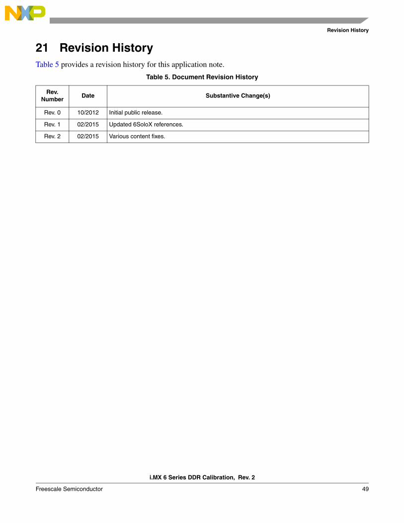
i.MX 6 Series DDR Calibration, Rev. 2
Freescale Semiconductor 49
Revision History
21 Revision HistoryTable 5 provides a revision history for this application note.
Table 5. Document Revision History
Rev. Number
Date Substantive Change(s)
Rev. 0 10/2012 Initial public release.
Rev. 1 02/2015 Updated 6SoloX references.
Rev. 2 02/2015 Various content fixes.
Document Number: AN4467Rev. 203/2015
Information in this document is provided solely to enable system and software
implementers to use Freescale products. There are no express or implied copyright
licenses granted hereunder to design or fabricate any integrated circuits based on the
information in this document.
Freescale reserves the right to make changes without further notice to any products
herein. Freescale makes no warranty, representation, or guarantee regarding the
suitability of its products for any particular purpose, nor does Freescale assume any
liability arising out of the application or use of any product or circuit, and specifically
disclaims any and all liability, including without limitation consequential or incidental
damages. “Typical” parameters that may be provided in Freescale data sheets and/or
specifications can and do vary in different applications, and actual performance may
vary over time. All operating parameters, including “typicals,” must be validated for each
customer application by customer’s technical experts. Freescale does not convey any
license under its patent rights nor the rights of others. Freescale sells products
pursuant to standard terms and conditions of sale, which can be found at the following
address: freescale.com/SalesTermsandConditions.
How to Reach Us:
Home Page: freescale.com
Web Support: freescale.com/support
Freescale and the Freescale logo are trademarks of Freescale Semiconductor, Inc., Reg. U.S. Pat. & Tm. Off. All other product or service names are the property of their respective owners. ARM is the registered trademark of ARM Limited. ARM CortexTM-A9 is the trademark of ARM Limited.
© 2015 Freescale Semiconductor, Inc.