implementation of a high-speed fpga and dsp based fft
TRANSCRIPT

November 2005
NASA/TM-2005-213791
Implementation of a High-Speed FPGA and DSP Based FFT Processor for Improving Strain Demodulation Performance in a Fiber-Optic-Based Sensing System Douglas L. Farley Langley Research Center, Hampton, Virginia

The NASA STI Program Office . . . in Profile
Since its founding, NASA has been dedicated to the advancement of aeronautics and space science. The NASA Scientific and Technical Information (STI) Program Office plays a key part in helping NASA maintain this important role.
The NASA STI Program Office is operated by Langley Research Center, the lead center for NASA’s scientific and technical information. The NASA STI Program Office provides access to the NASA STI Database, the largest collection of aeronautical and space science STI in the world. The Program Office is also NASA’s institutional mechanism for disseminating the results of its research and development activities. These results are published by NASA in the NASA STI Report Series, which includes the following report types:
• TECHNICAL PUBLICATION. Reports of
completed research or a major significant phase of research that present the results of NASA programs and include extensive data or theoretical analysis. Includes compilations of significant scientific and technical data and information deemed to be of continuing reference value. NASA counterpart of peer-reviewed formal professional papers, but having less stringent limitations on manuscript length and extent of graphic presentations.
• TECHNICAL MEMORANDUM. Scientific
and technical findings that are preliminary or of specialized interest, e.g., quick release reports, working papers, and bibliographies that contain minimal annotation. Does not contain extensive analysis.
• CONTRACTOR REPORT. Scientific and
technical findings by NASA-sponsored contractors and grantees.
• CONFERENCE PUBLICATION. Collected
papers from scientific and technical conferences, symposia, seminars, or other meetings sponsored or co-sponsored by NASA.
• SPECIAL PUBLICATION. Scientific,
technical, or historical information from NASA programs, projects, and missions, often concerned with subjects having substantial public interest.
• TECHNICAL TRANSLATION. English-
language translations of foreign scientific and technical material pertinent to NASA’s mission.
Specialized services that complement the STI Program Office’s diverse offerings include creating custom thesauri, building customized databases, organizing and publishing research results ... even providing videos. For more information about the NASA STI Program Office, see the following: • Access the NASA STI Program Home Page at
http://www.sti.nasa.gov • E-mail your question via the Internet to
[email protected] • Fax your question to the NASA STI Help Desk
at (301) 621-0134 • Phone the NASA STI Help Desk at
(301) 621-0390 • Write to:
NASA STI Help Desk NASA Center for AeroSpace Information 7121 Standard Drive Hanover, MD 21076-1320

National Aeronautics and Space Administration Langley Research Center Hampton, Virginia 23681-2199
November 2005
NASA/TM-2005-213791
Implementation of a High-Speed FPGA and DSP Based FFT Processor for Improving Strain Demodulation Performance in a Fiber-Optic-Based Sensing System Douglas L. Farley Langley Research Center, Hampton, Virginia

Available from: NASA Center for AeroSpace Information (CASI) National Technical Information Service (NTIS) 7121 Standard Drive 5285 Port Royal Road Hanover, MD 21076-1320 Springfield, VA 22161-2171 (301) 621-0390 (703) 605-6000
Acknowledgments
I would like to thank the members of the Safety Critical Avionics Systems Branch at NASA Langley, especially Jason Moore, Cuong Quach, and Sixto Vazquez for their help and patience during the course of this research. Their assistance was invaluable in completing this work.
The use of trademarks or names of manufacturers in the report is for accurate reporting and does not constitute an official endorsement, either expressed or implied, of such products or manufacturers by the National Aeronautics and Space Administration.

Acronyms and Glossary of Terms:
ALU Arithmetic Logic Unit AvSSP NASA’s Aviation Safety and Security Program CV Control Vector - Programming Language for the FFTDSP DDM Data Demodulation Module - Also the Original FOSS DDM during Comparisons DFT Discrete Fourier Transform DMA Direct Memory Access DSP Digital Signal Processing EDDM Enhanced Data Demodulation Module - DDM using FFTDSP Hardware FDDS FOSS Data Demodulation Software FFT Fast Fourier Transform FFTDSP PCI-X based FPGA/DSP combo card, used in the EDDM FFTW Fastest Fourier Transform in the West FOBG Fiber Optic Bragg Grating FOSS Fiber Optic Strain Sensor iFFT Inverse Fast Fourier Transform I/O Input/Output LaRC Langley Research Center ms Millisecond MSVC++ Microsoft Visual C++ NASA National Aeronautics and Space Administration PCI Peripheral Component Interconnect PCI-SIG PCI Special Interest Group - organization chartered to manage the PCI standard PCI-X Enhanced Specification of the PCI standard maintained by the PCI-SIG group RF Radio Frequency SHM Structural Health Management SDE Software Development Environment TFA Twiddle Factor Algorithm - Algorithm for processing large FFT's on the FFTDSP VHM Vehicle Health Management
iii

1
Abstract
NASA’s Aviation Safety and Security Program is pursuing research in on-board Structural Health Management (SHM) technologies for purposes of reducing or eliminating aircraft accidents due to system and component failures. Under this program, NASA Langley Research Center (LaRC) is developing a strain-based structural health-monitoring concept that incorporates a fiber optic-based measuring system for acquiring strain values. This fiber optic-based measuring system provides for the distribution of thousands of strain sensors embedded in a network of fiber optic cables. The resolution of strain value at each discrete sensor point requires a computationally demanding data reduction software process that, when hosted on a conventional processor, is not suitable for near real-time measurement. This report describes the development and integration of an alternative computing environment using dedicated computing hardware for performing the data reduction. Performance comparison between the existing and the hardware-based system is presented.
Introduction
Real time Structural Health Monitoring (SHM) is emerging as a key consideration in the design of future civilian and military aerospace vehicles. Envisioned SHM systems would provide time-critical diagnostic information necessary for avoiding catastrophic failure (e.g. Space Shuttle Columbia and Aloha 737 accident). In addition, such a system may allow for reduced conservatism in new designs, resulting in significant vehicle weight savings. One concept under investigation for SHM uses a network of densely distributed Fiber Optic Bragg Grating (FOBG) strain sensors [1], [2], [3]. These sensors are used primarily to measure strain but can be used to measure other physical parameters such as temperature, corrosion, and detection of hazardous gases [7], [8]. Fiber Optic Strain Sensors have benefits over traditional foil strain gauges in that they can be applied across a large area with a minimal weight penalty, are generally immune to moisture, and operate in the optical frequency ranges making them non-emissive and non-coupling in the RF region. This eliminates electromagnetic incompatibilities when integrated with RF sensitive systems.
A Fiber Optic Strain Sensor (FOSS) system has been developed at NASA’s Langley Research Center (LaRC) for data capture and analysis of FOBG-based sensor [4]. As described in [1], this system uses a demodulation approach that necessitates a large (220 discrete points) Fourier transform as a first step, followed by a series of inverse transforms in order to determine strain. Performing accurate and rapid Fourier transforms is essential for near real time operation in a VHM application.
This paper reports on one approach to reducing the time required that entails incorporating specialized hardware to increase the speed of calculating the Fourier transforms. Commercially available computing hardware specially optimized for performing Fast Fourier Transforms (FFT) was integrated into the FOSS system. A description of how this card was implemented into a new FOSS system is presented along with a comparison of its performance relative to the original system.

Original FOSS system
The current FOSS architecture [4] consists of three parts (Figure 1) a FOBG sensor array, an optical network, and a data demodulation module. For the purpose of this paper, the FOBG sensor array is bonded to the host structure (Figure 2), ensuring that the surface strain is sufficiently transferred to the fiber. The FOBG sensor array is connected to the optical network, which consists of the laser and optical circuit. The optical network transmits laser light from the FOBG array and converts the signals that are passed into the Data Demodulation Module (DDM). The DDM performs data acquisition, signal conversion, and strain derivation for each grating.
Data demodulation consists of the following five steps.
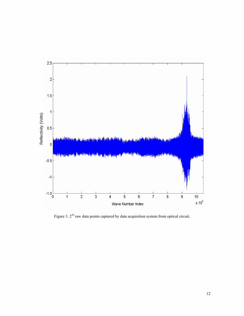
1. Data is acquired from the optical circuit (Figure 3 shows a sample data plot)
2. A 220 point FFT is performed on the acquired data (example plot are shown in Figure 4)
3. Data associated with individual Bragg gratings (example shown in Figure 4 insert) is extracted from the FFT transformed data.
4. An inverse FFT (iFFT) is performed upon each set of grating data (example results are shown in Figure 5)
5. Strain is calculated by the shift in the grating centroid as described in [4].
Three external signals are used by the data acquisition system to control data capture from the optical circuit. The three signals are the scan direction signal, the start pulse signal, and the reference clock signal that are output by the laser and optical network. The laser is a 10 milli-watt continuous-output, mode-hop-free, scanning laser that operates in a continuous monotonic scanning mode between 1530 nm and 1570 nm with a 150 kHz line-width [9]. With a combination of the start pulse signal and the up/down scan direction the timing on the grating can be determined, shown in Figure 6. An up scan is defined as the laser sweeping from 1530 nm to 1570 nm, and a down scan is the sweep from 1570 nm to 1530 nm. The reference clock signal, as seen in Figure 7, is used as a sample clock to drive the data acquisition.
The FOBG host structure is an instrumented beam test article (Figure 2) with a bonded Fiber containing 333 gratings along its length. The gratings are 6.5mm apart center to center, with each grating being approximately 4.5mm wide. When sampled, each captured grating consists of 224 data points. The sampled 224 points include head and tail noise (circled in Figure 8), around the grating ideal ‘top hat’ (dashed line region of the grating in Figure 8).
A significant limiting factor for performance in the DDM is the time required to process a 220 point FFT. The DDM, using the FFTW [6] libraries, calculates the 220 point FFT in 0.9 seconds. Furthermore an additional 0.4 seconds is required to compute the inverse FFT for all 333 gratings. Moreover, FFT computation takes approximately 1.3 seconds to demodulate 333 sensors using the existing conventional computing approach. With an increase in the density of the sensor network, the processing time will also increase. The increase in processing time can substantially vary depending on the addition of more gratings or more fibers.
2

Enhanced FOSS System
In an effort to improve strain demodulation performance in the fiber based sensing system, the original FOSS architecture was augmented with a PCI-X based FPGA/DSP combo card, which will be subsequently referred to as FFTDSP. The FFTDSP was integrated into a new host computer to perform the 220 point FFT and 224 point grating iFFT. The new computer hosting the FFTDSP board has a high speed PCI-X bus. The FFTDSP board was chosen because of its processing speed and the availability to use standard C/C++ routines for interfacing to the existing FOSS data demodulation software (FDDS). The FFTDSP board hardware consists of a PCI-X standard interface, an Altera EP1S20 FPGA core, and a DSP optimized for performing FFT and matrix operations. Also installed on the new host computer is a National Instruments PCI-6110 Data Acquisition Board, which is the same Data Acquisition Board used in the original DDM. For ease of comparison throughout the rest of this study, the original DDM will be referenced as the DDM, while the hardware enhanced DDM will be referenced as the EDDM.
New source code for supporting the integration of the FFTDSP was written in Microsoft Visual C++ (MSVC++) to retain consistency with the existing software environment. The object-oriented nature of the FDDS software design simplified the integration of the FFTDSP board into the FDDS. Only minimal modification to existing code was required in order to replace existing FFT functions with new hardware-accelerated replacement functions. The FFTDSP board has a specialized control vector (CV) language that provides primitives for matrix Arithmetic Logic Unit (ALU) operations as well as forward and inverse 2-D Fourier transforms. Programming the FFTDSP takes place within its own Software Development Environment (SDE). This SDE allows for compilation and debugging of the CV language using simulation and testing of real and modeled input. All data transferred to and from the FFTDSP’s 256MB onboard SDRAM is done via Direct Memory Access (DMA) calls from library routines included in the FFTDSP SDE.
To perform the FFT calculation in the FFTDSP, the 220 point 1-D vector (shown in cell 1 of Figure 9) is rearranged into a 2-D matrix form as required by the FFTDSP and shown in Cell 2 of Figure 9. Next, a Radix-2 Discrete Fourier Transform is applied to each 1024-point column vector (shown in cell 3 of Figure 9) after which each element within the square array is then multiplied by its respective Twiddle Factor, which are also known as roots of unity, (cell 4 of Figure 9) that is calculated by a sine or cosine term as represented by equation 1. After the multiplication of the Twiddle Factors, 1024 row major 1024 point FFT’s are performed on the 2-D data array (shown in cell 5 of Figure 9). Lastly, the resulting data is reordered into a 1-D array before being passed back to the calling function (shown in cell 6 of Figure 9). The code for such a 220 point FFT is shown in Figure 10, and is based upon a standard design for large FFT’s [5].
( ) ( )( )( ) jMcolumnrowecolumnrowtorTwiddleFac ⋅−−−= /112, π
McolumnMrow ,...,1;,...,1 ==
(Eq. 1) [5]
Equation 1 represents the Twiddle Factor Algorithm, where TwiddleFactor(row,column) is the value of the Twiddle Factor array at the specified row and column index; where row and column range from 1 to M, which is the maximum height of a row and column, and row and column form a square matrix. Equation 1 was modeled in C code by the following code segment.
3

Where “height” and “width” are the size of the modeled 2-D matrix, and “buffer” is the 1-D floating-point data structure for the Twiddle Factor. In our use of the Twiddle Factor Algorithm, both height and width were equal to M=1024. This code is based on the reference design provided for the DSPFFT [5].
for(k=0; k<height; k++) for(j=0; j<width; j++, ctr+=2) { buffer[ctr] = (float)cos(2*PI*k*j/(height*width)); buffer[ctr+1] = (float)sin(-2*PI*k*j/(height*width)); }
[5]
Once the 220 point FFT has been calculated, the inverse FFT (iFFT) must also be calculated. Calculating the iFFT required additional manipulation because the FFTDSP is optimized for large FFT arrays whose size is a power of 2 – the original system uses 224 points which is not a power of two. It was therefore decided to zero pad (fill) the data with 32 zero values to create a data set that was a power of 2 (224+32 = 256 = 28). Test cases of right, left and symmetrical end zero padding (as shown in Cell 1 of Figure 11) on post FFT grating data were conducted to evaluate the effect of zero padding on centroid calculation. Since the iFFT calculation is less than 1024 points, the Twiddle Factor Algorithm is not needed, and a simple FFT of the 256 data points can be performed instead. The calculated iFFT results are presented in Cell 2 of Figure 11 as well as a baseline case using 224 data points. Proportionality in centroid peak location is shown for each of the non-padded and padded data sets in Cell 2 of Figure 11. The symmetrical end padding technique was chosen for use in this study. The code used for the iFFT calculations for the grating data is shown in Figure 12. It should be noted that the matrix in Figure 12 is not square.
FOSS System Comparison
Evaluation of the EDDM entailed three studies: 1) a data demodulation timing study that compared the DDM to the EDDM system, 2) an FFTDSP sub-system timing study that analyzed specific steps within the FFTDSP independent from the DMA transfers, and 3) a strain verification study that compared the differences between the DDM and the EDDM relative to calculated strain value.
The DDM timing study was designed to compare the performance between the DDM and EDDM gained through the addition of optimized FFT computing hardware to augment the DDM. This was accomplished by comparing the FFT performance time of the DDM and the EDDM systems. Both systems sampled eight data sets in parallel and performed calculations in parallel, taking the next sample when the previous data set was processed. This approach ensured that processing time differences were not dependent on the data set used and also allowed for a comparison of numerical calculations. Execution time was calculated by comparing the start and end wall clock time before and after the call to the FFT and iFFT functions within the FFTDSP and FFTW modules. The DDM using the FFTW performs the FFT without additional data transfer. The EDDM includes the passing the 220 set of data as an array using a DMA transfer to the FFTDSP, the FFTDSP FFT calculations, and a DMA transfer returning the results back to the host. The DDM was timed on both the original (existing) DDM system, and the new computer hosting the FFTDSP hardware. The EDDM could only be timed on the new host, as the original did not meet the minimum hardware requirements for the FFTDSP board.
4
The FFTDSP sub-system timing study was designed to establish a time budget within the EDDM for selected FFTDSP native CV code functions. The FFTDSP SDE provides the necessary methods to test the native CV code with real or simulated data. The SDE consists of a code input module, and a code test module. The code input module allows for writing and debugging the native CV code blocks such as Figure 10 and Figure 12 with the aid of a native CV compiler. The test module provides an environment to test the compiled CV code in a simulated mode or on the FFTDSP. The SDE test module also provides a timing function for establishing estimated and actual runtimes of a native CV code process. In order to accurately gauge the run time, multiple repetitions of the native CV code sub-functions were performed within the 220 FFT routine.
The strain calculation study was designed to allow comparison of the calculated strain between DDM and EDDM systems. The goal of these comparisons was not to analyze the μ-strain measurement system (this study was covered extensively in [1], [2], [4]), but rather to verify that the enhanced system produced results commensurate with the DDM. To perform such a comparison, both the DDM and EDDM systems collected data in parallel from an instrumented test article subjected to a static load.
Discussion of Results
Timing studies were conducted within both FOSS DDM and EDDM. To characterize the performance of specialized computing components a study was conducted using the FFTDSP SDE. An assesment of the accuracy of the FFTDSP strain results compared to the FFTW data is also presented.
Data Demodulation Timing Study
In order to compare the performance of the DDM C++ code routines, wall clock time, established through the judicial insertion of the native C++ function clock(), was selected as the standard approach for measuring runtime. The difference in two returned values from clock() divided by the constant CLOCKS_PER_SEC (1000) returns the elapsed time in seconds. This method imposes minimal error in the time calculation due to function call overhead. The clock() function was inserted in similar locations in both the DDM and the EDDM. These calls were placed around the routine for calling the FFTDSP in the EDDM and the FFTW libraries in the DDM routines at the 220 point FFT and the 256 point grating iFFT, respectively. The results of the Data Demodulation Timing study are presented in Figure 13 and plotted in Figure 14.
On average the DDM, running on the original host, was able to process the full 220 point FFT in approximately 0.855 seconds, as given in Figure 13. The average processing time of the inverse FFT grating data by the DDM system was approximately 0.360 seconds. The total time to calculate both the 220 point FFT and the grating iFFT’s was then 1.215 seconds, or 0.823 Hz, using the DDM system (as shown in Figure 13). These numbers provide a reference point for the performance of the DDM code.
In order to assess the performance of the FFTW libraries, they were additionally tested on the new computer system that hosts the FFTDSP board. The 220-point FFT calculation required 0.120 seconds (Figure 13), or 85 percent faster than the reference DDM 220-point FFT. The average processing time of the iFFT grating data was 0.0782 seconds. As in the original DDM system, there is no DMA transfer required to perform the FFT and iFFT on the data. The total time spent processing both the 220-point FFT and 333 256-point iFFTs was 0.198 second or 5 Hz (as shown in Figure 13), which is 83 percent faster than the reference DDM.
5
The EDDM system was able to process the full 220 point FFT in approximately 0.250 seconds or 70 percent faster than the reference DDM 220-point FFT, as depicted in Figure 14. This 0.250 second time includes data transfer in and out of the board. Processing the 333 iFFT calculations on the EDDM system requires between 0.253 to 0.540 seconds. Upon closer examination, it was discovered that DMA timeouts occurred approximately in 1 of 600 cases during data transfers for the 256-point iFFTs. These timeouts could be the result of the small size of the iFFT data sets (256 points) and the relatively fast turn around speed for successive iFFT calculations, setting up a condition whereby at certain times the DMA is still flagged as busy when the next call is issued. This sporadic wait and retry accounts for approximately 0.287 seconds of timeout delay, resulting in a total of 0.540 seconds to perform all 333 iFFTs. Without these DMA timeouts, the whole grating set would process in approximately 0.253 seconds, or 0.000757 seconds per grating (0.253 seconds divided by 333 total gratings). In addition, without the errors, the FFT and iFFT routines processed by the FFTDSP on the EDDM system would only take approximately 0.500 seconds or 60 percent faster than the reference DDM. With the errors, the computation requires approximately 0.786 seconds (as shown in Figure 13) or 35 percent faster than the reference DDM. Considering the DMA errors that occurred with the EDDM results, the FFTW-based DDM on the new host provides the best performance.
FFTDSP SDE Timing Study
To further understand the impact of the DMA transfer on the FFT timing in the EDDM a more detailed timing study was conducted using the FFTDSP SDE on the 220 point FFT. The time budget of a DMA transfer in the 220 FFT case presumably scales down to the 256 point iFFT assuming no DMA timeouts. The 220 point FFT can be generalized into three steps: Load (consisting of LoadData and LoadTwiddles routines in Figure 10), FFT (consisting of StartFFT1D in Figure 10), and Save (consisting of OutputData in Figure 10). The FFTDSP SDE allows for timing of individual routines to better assess the runtimes of each element in the processes of performing an FFT. However, it is too coarse for ascertaining the timing of the FFT step. For example, in the StartFFT1D routine, the timer returns values of 0.0 seconds for each execution. Although the resulting data is correct, within the limitations of the timing function, the timing result is clearly due to round-off error. Therefore, it is necessary to combine the FFT with other steps and subtract out the contribution of these other steps to calculate an average FFT time. Clearly, this approach has its limitations.
Since the SDE provides for the preloading of specific data on the FFTDSP, it is possible to independently evaluate the time required to perform computation on the data or the saving of data. The SDE also provides a looping construct that allows for executing a step a prescribed number of times while collecting timing data. Initially the FFT step was tested solely with this loop construct to extract the timing. However, the returned time was an order of magnitude less than the manufacturers reported time. The time difference in the extracted time and the advertised processing time can be attributed to internal overhead not accounted for by using loop construct solely around the FFT step. Therefore six separate permutations of steps were tested, namely the Load, Save, Load+Save, Load+FFT, FFT+Save, and Load+FFT+Save. The results of the FFTDSP sub-system timing study are presented in Figure 15. Each permutation was looped 10 times and averaged. The average time required to perform the full case (Load+FFT+Save) was approximately 0.253 seconds (Figure 15), remarkably similar to the 0.253 second average from the EDDM. Using these six data points, three separate values for the FFT time were extracted (Figure 16). These three values were then averaged to obtain an average FFT runtime of 0.024 seconds shown in Figure 16, which corresponds to the manufacturers reported time. This study shows that the FFTDSP is 80 percent faster than the FFTW routines on the new computer system. By deduction, out of the 0.253 seconds for all three steps, 0.024 seconds is used for the FFT, the remaining 90 percent is allocated to DMA transfers. Based upon the run-time extraction the average Load time is 0.207 seconds, whereas the average Save time is 0.018 seconds. Notable is the fact that the Save time is significantly
6

less than the Load time which is likely due to caching of returned data along the bus path.
An approach to reducing data transfer time and eliminating the DMA timeout is to perform the iFFTs immediately after the FFT in-place on the FFTDSP. If the FFT and iFFT calculations were performed in hardware, the resulting time budget would consist of a Load, 220 point FFT, 333 256-point inplace iFFTs, and a Save, eliminating the observed DMA timeouts from the iFFT data transfers. Timing results for all these steps are shown in Figure 15 and Figure 16 except for the iFFT time. However, by applying the 90 percent DMA to 10 percent FFT ratio to the total iFFT time of 0.253 seconds (Figure 13) a new total iFFT time of 0.0253 seconds is derived. The 0.0253 second iFFT time excludes the need for DMA transfer between gratings. The total time projected for these steps would be 0.2753 seconds. This total calculated time is comprised of 10 percent of the iFFT time and 100 percent of the FFT time.
Including DMA time-out overhead, the EDDM performs at 1.2 Hz (Figure 13), which is 35 percent faster than the reference DDM system. At 0.275 seconds for a single analysis, it would be possible to perform analysis around 3.64 Hz or 77 percent faster than the reference DDM. While the new approach is 30 percent slower to perform the full analysis than FFTW on the new host, the majority of this time is spent in DMA. The new approach still performs the core FFT operations 65 to 80 percent faster in the iFFT and FFT respectively than the FFTW core on the new host. This type of hardware FFT solution approaches the performance necessary to monitor the health of large structures.
Strain Comparison
Both the EDDM and DDM were run to generate comparable strain values for a cantilevered test beam subjected to a 1.4 kg load on the free end (non-loaded beam shown in Figure 2). In these tests both EDDM and DDM implementations calculated similar strain results, as shown in Figure 17. Statistical correlations on the strain values show a 0.998 correlation between the EDDM and DDM calculated results. While this analysis is not intended to be a review of the strain calculations, which are thoroughly covered in [4], the results show that the results of the EDDM system are accurate to the DDM baseline.
Conclusions
The objective of this study was to characterize the performance benefits gained by replacing certain software modules in LaRC’s DDM with a high-speed FPGA and DSP-based FFT hardware accelerator. The hardware-accelerated system showed comparable performance to the software-only system with negligible impact on data accuracy, while taking the largest penalty in DMA transfer.
With the study of the FFTDSP SDE timing data, it is evident that a purely hardware based solving method to the 220 point FFT is faster than the software system. While the EDDM system outperforms the original DDM, the FFTW library running on the new host system is able to perform the total operation in only 0.198 seconds, a 60 percent increase in performance over the EDDM. The performance of the EDDM system was still lower than anticipated when DMA timeouts removed from the time computation. It should be noted however that even with the DMA errors removed, the total processing time of the EDDM system is still bound by the DMA Load and Save operations, and the core FFT operations are still performed faster on the FFTDSP than with the FFTW. What this study does not show is the possible benefits of being able to offload the data processing of the DDM from the host, freeing up the resources of the host during this period. Eliminating some of the DMA transfer overhead from the iFFTs and Save from the 220-point FFT can further increase performance.
7

Future improvements in the speed of embedded FPGA and DSP technology as well as improvements in the FOSS system will soon allow for even faster and efficient processing of such systems to be invaluable assets to failure mitigation and vehicle health monitoring. Effort will also be focused on eliminating as many DMA transfers as possible, since over half of the processing time is used to transfer data to and from the FFTDSP. Without such adjustments, the performance of the software FFTW library in place of the hardware approach will continue to be a more efficient solution.
Possible Future Research
Through the course of research into a hardware accelerated DDM further performance gains using the FFTDSP accelerated DDM are possible. The FFTDSP includes two separate Altera Stratix processors that handle the memory control functions and the ALU and matrix operations that are not performed by the DSP. Reconfiguring the FFTDSP to easily perform the entire calculations without intermediate data transfers would also improve performance. The manufacturer literature states that approximately 45 percent of the onboard gates are unused and available for programming on the FPGAs. With the ability to write code to these free gates, it could be possible to implement the entire FOSS code set in hardware.
While the FPGAs currently are not directly accessible, the manufacturer does provide the FFTDSP SDE interface. This interface allows access to ALU operations and primitive functions on the FFTDSP with the Control Vector programming language allows further flexibility that remains unexplored. For example, the zero filling of the grating data vectors before the inverse FFT could be efficiently performed on the FFTDSP, avoiding having to be performed prior to DMA transfer. Additionally, the CV language permits the use of subset matrices that can be addressed within larger matrices. In a fixed size system, such as on a vehicle, it would then be possible for each grating to be extracted directly from the FFTDSP. Such programming would allow each calculation of the inverse FFT to be performed on the FFTDSP, and then a single DMA transfer of all the grating inverses back to the software for calculation of each centroid and the individual strain values.
Furthermore, a large effort was put forth to ensure compatibility with the original FOSS DDM system with the FFTDSP card. A standalone application could be developed in the future that did not retain such compatibility providing faster results with less overhead.
8

References:
[1] Mark Froggatt, Jason Moore, “Distributed Measurement of Static Strain in an Optical Fiber with Multiple Bragg Gratings at Nominally Equal Wavelengths”, Applied Optics-OT, Vol. 37, Issue 10, Page 1741 (April 1998)
[2] Brook A. Childers, Mark E. Froggatt, Sidney G. Allison, Thomas C. Moore, Sr., David A. Hare, Christopher F. Batten, Dawn C. Jegley, “Use of 3000 Bragg Grating Strain Sensors Distributed on Four Eight-Meter Optical Fibers During Static Load Tests of a Composite Structure”, SPIE's 8th International Symposium on Smart Structures and Materials, Newport Beach, California, March 4-8, 2001.
[3] Devendra S. Parmar, Danny R. Sprinkle and Jag J. Singh, “Development of In-Fiber Reflective Bragg Gratings as Shear Stress Monitors in Aerodynamic Facilities”, NASA/TP-1998-207643, April 1998.
[4] Cuong C. Quach and Sixto L. Vazquez, “Comparison of Fiber Optic Strain Demodulation Implementations”, NASA/TM-2005-213521, March 2005.
[5] MatLab Users Guide for FFT Signal Processing Blockset [online]. The MathWorks, Inc., 2005 [cited 16 June 2005]. Available from World Wide Web: (http://www.mathworks.com/access/helpdesk/help/toolbox/dspblks/fft.html)
[6] FFTW: Fastest Fourier Transform in the West [online]. Massachusetts Institute of Technology, 2005 [cited 7 April 2005]. Available from World Wide Web: (http://www.fftw.org/)
[7] Thomas E. Munns, Renee M. Kent, Antony Bartolini, Charles B. Gause, Jason W. Borinski, Jason Dietz, Jennifer L. Elster, Clark Boyd, Larry Vicari, Kevin Cooper, Asok Ray, Eric Keller, Vadlamani Venkata and S. C. Sastry, “Health Monitoring for Airframe Structural Characterization”, NASA/CR-2002-211428, February 2002
[8] Kersey, Alan D., Davis, Michael A., Patrick, Heather J., LeBlanc, Michel, Koo, K. P., Askins, C. G., Putnam, M. A., Friebele, E. Joseph, “Fiber Grating Sensors”, Journal of Lightwave Tech., 15(8), 8 August 1997.
[9] “Tunics-Plus: Tunable External Cavity Laser Instruction Manual”, Doc MU#3642/DSC/008/B, Product Manual, NetTest A/S, 2002.
9

Figure 1. Block diagram of FOSS system architecture.
10

FOSS Fiber
FOSS Fiber
Figure 2. Host structure (cantilevered beam) with bonded Bragg grated fiber running up and down length.
11
Ref
lect
ivity
(Vol
ts)
Figure 3. 220 raw data points captured by data acquisition system from optical circuit.
12

Grating #2
Ref
lect
ivity
(Arb
)
Ref
lect
ivity
(Arb
)
Distance Along Fiber (m)
Distance Along Fiber (m)
Figure 4. Power spectrum of the Fourier Transform result showing response of gratings 1 through 5 in insert with grating 2 highlighted.
13

Distance Along Fiber (Index)
Ref
lect
ivity
Figure 5. Grating 2 in power spectrum and reflected power spectrum form after the iFFT.
14

Seconds
Vol
tage
Figure 6. Oscilloscope timing diagram of the scan direction and start pulse signals from the laser.
Seconds
Vol
tage
Figure 7. Reference clock signal.
15

Head Tail
Top Hat
Figure 8. Circled Head and tail grating signal and dashed ‘Top Hat’ outline of grating signal.
16

DSPFFT Operations
Figure 9. Twiddle Factor Discrete Fourier Transform Algorithm block diagram showing the process for a 220-point DFT using the FFTDSP PCI-X card in the FOSS EDDM.
17

/*FFT input */ input datain(1024,1024, IEEE_CPLX); input twiddles(1024,1024,IEEE_CPLX); output FFTresult(1024,1024,IEEE_CPLX,0); auto dataP1(P1,0,0); auto twiddlesP2(P2,0,0); auto interP3(P3,0,0); auto resP4(P4,0,0); cv LoadData{ /* Load User Input Data */ dataP1.H = datain.H; /* Load from datain, and store to dataP1 Horiz */ } cv LoadTwiddles { /* Load Twiddle Data*/ twiddlesP2.H = twiddles.H; /* Read in from Ibuff and store to membuf horiz */ } cv StartFFT1D{ /* Process the FFT */ interP3.V = fft(1 * dataP1.V); /* FFT Column Major */ resP4.H = fft(interP3.H * twiddlesP2.H); /* Mul by twiddle then Col Major FFT */ } cv OutputData{ /* Write Data Out */ FFTresult.H = resP4.V; /* FFT result horiz to Obuff */ }
Figure 10. Example CV code for FFTDSP 220 point FFT
18

Distance Along Fiber (Index)
Ref
lect
ivity
(Arb
)
Wave Number (Index)
Gra
ting
Ref
lect
ed P
ower
(Arb
) Grating Response In
Spatial Domain
Grating Response In Wave Number Domain
Cell 1
Cell 2
Figure 11. The effect of zero padding (256 data point sets) and the original 224 point data set with the iFFT of an individual grating. (Cell 1) Grating data padding cases after FFT. (Cell 2) Grating data padding cases after iFFT.
19

/* Grating iFFT – 256 Points */ input userdata(256,1, IEEE_CPLX); output result(256,1,IEEE_CPLX,0); auto resP4(P4,0,0); cv ShortFFT1D{ /* iFFT Routine */ resP4.H = ifft(1 * userdata.H); /* ifft data */ result.H = resP4.H; /* Output data */ }
Figure 12. Example CV code for FFTDSP 256 point grating iFFT.
Data Demodulation Timing Study
DDM
Reference (FFTW)
FFTW On New Host
EDDM (FFTDSP)
EDDM With DMA Errors
Run-Time for 220-point FFT (milliseconds) 855 ms 120 ms 250 ms 250 ms
Time for 333, 256-point grating iFFT’s (milliseconds)
360 ms 78.2 ms 253 ms 540 ms
Total Time Per Analysis (milliseconds) 1215 ms 198.2 ms 503 ms 790 ms
Total Processing Frequency .823 Hz 5.04 Hz 2 Hz 1.27 Hz
Figure 13. Table of Results from Data Demodulation Timing Study.
20

FOSS Data Demodulation Timing Study
0
0.1
0.2
0.3
0.4
0.5
0.6
0.7
0.8
0.9
Tim
e (s
)
DDM - Orig. Host EDDM - New Host DDM - New Host
220 Point FFT Grating iFFT
Figure 14. Timing study between FFTW and FFTDSP implementations of the FOSS Data Demodulation Modules.
21

Permutation Average Permutation Run-time per loop with 10 loops
Load 207.8 ms Save 18.7 ms
Load+Save 228.1 ms
Figure 15. FFTDSP SDE based timing study showing the average permutation time cases of the native CV code routines for the 220 FFT.
Load+FFT 229.7 ms FFT+Save 42.5 ms
Load+FFT+Save 253.1 ms
Permutation Average FFT Run-time Derived from Permutation Load+FFT 21.9 ms FFT+Save 23.8 ms
Load+FFT+Save 26.6 ms
Average FFT 24.1 ms
Figure 16. 220-point FFT runtime averages extrapolated from FFTDSP SDE based timing study
22

Strain Comparison Between FFTDSP and FFTW Implementations
0
100
200
300
400
500
600
0 5 10 15 20 25 30 35 40 45
Distance (In)
μ-Strain
FFTDSP FFTW
Figure 17. Strain graph of returned data from FFTDSP and FFTW FOSS DDM along with respective polynomial fit lines.
23

REPORT DOCUMENTATION PAGE Form ApprovedOMB No. 0704-0188
2. REPORT TYPE Technical Memorandum
4. TITLE AND SUBTITLE
Implementation of a High-Speed FPGA and DSP Based FFT Processor forImproving Strain Demodulation Performance in a Fiber-Optic-BasedSensing System
5a. CONTRACT NUMBER
6. AUTHOR(S)
Douglas L. Farley
7. PERFORMING ORGANIZATION NAME(S) AND ADDRESS(ES)
NASA Langley Research CenterHampton, VA 23681-2199
9. SPONSORING/MONITORING AGENCY NAME(S) AND ADDRESS(ES)
National Aeronautics and Space AdministrationWashington, DC 20546-0001
8. PERFORMING ORGANIZATION REPORT NUMBER
L-19152
10. SPONSOR/MONITOR'S ACRONYM(S)
NASA
13. SUPPLEMENTARY NOTESAn electronic version can be found at http://ntrs.nasa.gov
12. DISTRIBUTION/AVAILABILITY STATEMENTUnclassified - UnlimitedSubject Category 35Availability: NASA CASI (301) 621-0390
19a. NAME OF RESPONSIBLE PERSON
STI Help Desk (email: [email protected])
14. ABSTRACT
NASA’s Aviation Safety and Security Program is pursuing research in on-board Structural Health Management (SHM)technologies for purposes of reducing or eliminating aircraft accidents due to system and component failures. Under thisprogram, NASA Langley Research Center (LaRC) is developing a strain-based structural health-monitoring concept thatincorporates a fiber optic-based measuring system for acquiring strain values. This fiber optic-based measuring systemprovides for the distribution of thousands of strain sensors embedded in a network of fiber optic cables. The resolution ofstrain value at each discrete sensor point requires a computationally demanding data reduction software process that, whenhosted on a conventional processor, is not suitable for near real-time measurement. This report describes the development andintegration of an alternative computing environment using dedicated computing hardware for performing the data reduction.Performance comparison between the existing and the hardware-based system is presented.15. SUBJECT TERMSBragg grating; DSP; Demodulation; Fiber optic; Software; Strain sensors
18. NUMBER OF PAGES
2919b. TELEPHONE NUMBER (Include area code)
(301) 621-0390
a. REPORT
U
c. THIS PAGE
U
b. ABSTRACT
U
17. LIMITATION OF ABSTRACT
UU
Prescribed by ANSI Std. Z39.18Standard Form 298 (Rev. 8-98)
3. DATES COVERED (From - To)
5b. GRANT NUMBER
5c. PROGRAM ELEMENT NUMBER
5d. PROJECT NUMBER
5e. TASK NUMBER
5f. WORK UNIT NUMBER
23-079-30-11
11. SPONSOR/MONITOR'S REPORT NUMBER(S)
NASA/TM-2005-213791
16. SECURITY CLASSIFICATION OF:
The public reporting burden for this collection of information is estimated to average 1 hour per response, including the time for reviewing instructions, searching existing data sources, gathering and maintaining the data needed, and completing and reviewing the collection of information. Send comments regarding this burden estimate or any other aspect of this collection of information, including suggestions for reducing this burden, to Department of Defense, Washington Headquarters Services, Directorate for Information Operations and Reports (0704-0188), 1215 Jefferson Davis Highway, Suite 1204, Arlington, VA 22202-4302. Respondents should be aware that notwithstanding any other provision of law, no person shall be subject to any penalty for failing to comply with a collection of information if it does not display a currently valid OMB control number.PLEASE DO NOT RETURN YOUR FORM TO THE ABOVE ADDRESS.
1. REPORT DATE (DD-MM-YYYY)
11 - 200501-