fpga-based dsp system
TRANSCRIPT

Computer Engineering Senior Project
FPGA-Based DSP System
Final Report
AuthorAaron Nguyen
AdvisorDr. Wayne Pilkington
June 2018

Table of Contents
List of Figures 3
List of Tables 3
Listings 3
Abstract 4
1 Introduction 51.1 Overview . . . . . . . . . . . . . . . . . . . . . . . . . . . . . . . . . . . . . 51.2 Motivation . . . . . . . . . . . . . . . . . . . . . . . . . . . . . . . . . . . . . 51.3 Description of Potential Customer . . . . . . . . . . . . . . . . . . . . . . . . 51.4 Customer Needs . . . . . . . . . . . . . . . . . . . . . . . . . . . . . . . . . . 51.5 System Context . . . . . . . . . . . . . . . . . . . . . . . . . . . . . . . . . . 51.6 Alternative/Competitor Solutions . . . . . . . . . . . . . . . . . . . . . . . . 5
2 Background 72.1 FPGA . . . . . . . . . . . . . . . . . . . . . . . . . . . . . . . . . . . . . . . 72.2 FIR Filter . . . . . . . . . . . . . . . . . . . . . . . . . . . . . . . . . . . . . 72.3 IP Cores . . . . . . . . . . . . . . . . . . . . . . . . . . . . . . . . . . . . . . 7
2.3.1 Clock Wiz . . . . . . . . . . . . . . . . . . . . . . . . . . . . . . . . . 72.3.2 DDS Compiler . . . . . . . . . . . . . . . . . . . . . . . . . . . . . . 8
2.4 I2S Protocol . . . . . . . . . . . . . . . . . . . . . . . . . . . . . . . . . . . . 8
3 Product Design Engineering Requirements 103.1 Functional Requirements . . . . . . . . . . . . . . . . . . . . . . . . . . . . . 103.2 Minimum Performance Specifications . . . . . . . . . . . . . . . . . . . . . . 103.3 User Interface . . . . . . . . . . . . . . . . . . . . . . . . . . . . . . . . . . . 10
4 System Design - Functional Decomposition (Level 1) 114.1 Overall System Functional Block Diagram . . . . . . . . . . . . . . . . . . . 12
5 Technology Choices and Design Approach Alternatives Considered 135.1 Main Processor . . . . . . . . . . . . . . . . . . . . . . . . . . . . . . . . . . 135.2 Input and Output . . . . . . . . . . . . . . . . . . . . . . . . . . . . . . . . . 13
6 Project Design Description 146.1 ADC . . . . . . . . . . . . . . . . . . . . . . . . . . . . . . . . . . . . . . . . 14
6.1.1 Theory of Operation . . . . . . . . . . . . . . . . . . . . . . . . . . . 146.1.2 Specifications . . . . . . . . . . . . . . . . . . . . . . . . . . . . . . . 14
6.2 Filter . . . . . . . . . . . . . . . . . . . . . . . . . . . . . . . . . . . . . . . 146.2.1 Theory of Operation . . . . . . . . . . . . . . . . . . . . . . . . . . . 14
1

6.3 DAC . . . . . . . . . . . . . . . . . . . . . . . . . . . . . . . . . . . . . . . . 156.3.1 Theory of Operation . . . . . . . . . . . . . . . . . . . . . . . . . . . 156.3.2 Specifications . . . . . . . . . . . . . . . . . . . . . . . . . . . . . . . 15
6.4 System . . . . . . . . . . . . . . . . . . . . . . . . . . . . . . . . . . . . . . . 166.4.1 Theory of Operation . . . . . . . . . . . . . . . . . . . . . . . . . . . 16
7 Physical Implementation & Packaging Concept 177.1 Hardware Configuration/Layout . . . . . . . . . . . . . . . . . . . . . . . . . 17
8 Project (System-Level) Verification Test Plan 188.1 ADC Driver . . . . . . . . . . . . . . . . . . . . . . . . . . . . . . . . . . . . 188.2 DAC Driver . . . . . . . . . . . . . . . . . . . . . . . . . . . . . . . . . . . . 188.3 Filter Driver . . . . . . . . . . . . . . . . . . . . . . . . . . . . . . . . . . . . 198.4 System . . . . . . . . . . . . . . . . . . . . . . . . . . . . . . . . . . . . . . . 218.5 Summary . . . . . . . . . . . . . . . . . . . . . . . . . . . . . . . . . . . . . 26
9 Conclusions 27
Bibliography 28
Appendix 29
A Analysis of Senior Project Design 29A.1 Summary of Functional Requirements . . . . . . . . . . . . . . . . . . . . . . 29A.2 Primary Constraints . . . . . . . . . . . . . . . . . . . . . . . . . . . . . . . 29A.3 Econonomic . . . . . . . . . . . . . . . . . . . . . . . . . . . . . . . . . . . . 29A.4 If manufactured on a commercial basis . . . . . . . . . . . . . . . . . . . . . 30A.5 Environmental . . . . . . . . . . . . . . . . . . . . . . . . . . . . . . . . . . 30A.6 Manufacturability . . . . . . . . . . . . . . . . . . . . . . . . . . . . . . . . . 30A.7 Sustainability . . . . . . . . . . . . . . . . . . . . . . . . . . . . . . . . . . . 31A.8 Ethical . . . . . . . . . . . . . . . . . . . . . . . . . . . . . . . . . . . . . . . 31A.9 Health and Safety . . . . . . . . . . . . . . . . . . . . . . . . . . . . . . . . . 31A.10 Social and Political . . . . . . . . . . . . . . . . . . . . . . . . . . . . . . . . 31A.11 Development . . . . . . . . . . . . . . . . . . . . . . . . . . . . . . . . . . . 32
B Parts List and Costs 33B.1 Prototype . . . . . . . . . . . . . . . . . . . . . . . . . . . . . . . . . . . . . 33
C Project Schedule 34
D PCB Design 35D.1 Schematic . . . . . . . . . . . . . . . . . . . . . . . . . . . . . . . . . . . . . 35D.2 Layout . . . . . . . . . . . . . . . . . . . . . . . . . . . . . . . . . . . . . . . 36
E VHDL Source Code 37
2

List of Figures1 I2S Protocol Timing Diagram . . . . . . . . . . . . . . . . . . . . . . . . . . 82 Level 0 Block Diagram for FPGA DSP System . . . . . . . . . . . . . . . . . 103 Level 1 Block Diagram for FPGA DSP System . . . . . . . . . . . . . . . . . 124 Direct Form 1 FIR Filter Block Diagram . . . . . . . . . . . . . . . . . . . . 155 Complete Physical Design . . . . . . . . . . . . . . . . . . . . . . . . . . . . 176 ADC Behavioral Simulation . . . . . . . . . . . . . . . . . . . . . . . . . . . 187 DAC Behavioral Simulation . . . . . . . . . . . . . . . . . . . . . . . . . . . 188 Filter Expected Response (9 Tap Moving Average) . . . . . . . . . . . . . . 199 Filter Behavioral Simulation — 21.4 kHz Input . . . . . . . . . . . . . . . . 2010 Filter Behavioral Simulation — 6.5 kHz Input . . . . . . . . . . . . . . . . . 2011 System Post-Implementation Simulation . . . . . . . . . . . . . . . . . . . . 2112 Clock Signals (ADC and DAC), ADC Input Grounded . . . . . . . . . . . . 2213 Output — ADC Connected, No ADC Input . . . . . . . . . . . . . . . . . . 2214 Output — Frequency Response, ADC Connected No ADC Input . . . . . . . 2315 Output — 500 Hz Sinusoid Input, Filter Disabled . . . . . . . . . . . . . . . 2416 Output — 500 Hz Sinusoid Input, Filter Enabled . . . . . . . . . . . . . . . 2417 Output — Multiple Sinusoid Input, Filter Disabled . . . . . . . . . . . . . . 2518 Output — Multiple Sinusoid Input, Filter Enabled . . . . . . . . . . . . . . 2519 Time Estimate Schedule . . . . . . . . . . . . . . . . . . . . . . . . . . . . . 3420 Actual Schedule . . . . . . . . . . . . . . . . . . . . . . . . . . . . . . . . . . 3421 ADC Module Schematic . . . . . . . . . . . . . . . . . . . . . . . . . . . . . 3522 Layout and Implementation of ADC PCB Module . . . . . . . . . . . . . . . 36
List of Tables1 ADC Functional Requirements . . . . . . . . . . . . . . . . . . . . . . . . . 112 FPGA Functional Requirements . . . . . . . . . . . . . . . . . . . . . . . . . 113 DAC Functional Requirements . . . . . . . . . . . . . . . . . . . . . . . . . . 114 System Prototype BOM . . . . . . . . . . . . . . . . . . . . . . . . . . . . . 33
Listings1 System Wrapper Code . . . . . . . . . . . . . . . . . . . . . . . . . . . . . . 372 Clock Driver . . . . . . . . . . . . . . . . . . . . . . . . . . . . . . . . . . . . 403 ADC Driver . . . . . . . . . . . . . . . . . . . . . . . . . . . . . . . . . . . . 414 Filter Driver . . . . . . . . . . . . . . . . . . . . . . . . . . . . . . . . . . . . 425 DAC Driver . . . . . . . . . . . . . . . . . . . . . . . . . . . . . . . . . . . . 45
3

Abstract
The purpose of this project is to create a modular FPGA-based filtering system foraudio in VHDL. The final implementation has a working input, output, and filteringsystem but the filtering system still must be fine-tuned.
4

1 Introduction
1.1 OverviewThis project implements a filtering system on the Nexys 4 DDR board. It receiives one input(stereo 3.5mm or RCA), filters it with the FPGA, and then outputs the result to a stereo3.5mm jack.
1.2 MotivationThe purpose of this product is to allow for simple synthesis of an FIR filter in an FPGA ratherthan a DSP chip. Since this is a relatively niche product in its current state, the customerwill likely use it to analyze and compare FPGA-based filters with DSP chip-based filters.The main problem it solves for the customer is the customer does not have to implementthe entire filtering system from scratch; the input and output methods are already designedand a base filter driver is already given. The example logic is already within the filter driverand it can easily be changed from its current direct form I structure to another structure byfollowing the example syntax and logic.
1.3 Description of Potential CustomerIn its current state, the primary customer for this product would be students in an educationalenvironment. The filter is completely programmable and can be easily converted to anotherfilter form. Input and output logic are already taken care of and do not need to be worriedabout.
1.4 Customer NeedsThe customer/market requirements are as follows:
• Quick filter disabling method for comparison of filtered signal vs unfiltered signal.
• Programmable VHDL-based filtering.
• Relatively simple to use.
1.5 System ContextSince this project is solely a DSP unit, it must sit in-between a line-level output device (e.g.pre-amplifier or computer) and the device to be outputted to. The system ideally outputs asignal with magnitude equal to the signal coming in.
1.6 Alternative/Competitor SolutionsThe main competitor for this product are the devices created by MiniDSP. MiniDSP productsutilize discrete DSP chips rather than FPGAs though, so their performance is limited. The
5

MiniDSP 2x4 HD, for example, can have a maximum of ten parametric filters on each inputchannel and ten parametric filters on each output channel, or they can utilize a maximum1024 tap FIR filter.
This solution can easily exceed a 1024 tap filter but it can only be programmed viaputting in filter coefficients line by line.
6

2 Background
2.1 FPGAAn FPGA, or a field-programmable gate array, is an integrated circuit with programmabletransistor-level logic. It can be programmed with a hardware design language such as VHDLor Verilog. The primary benefit of FPGAs is that they can have multiple processes that runin parallel with sequential ”code” running inside the processes.
2.2 FIR FilterAn FIR Filter is a filter whose response ends in a finite amount of time. In general, an FIRfilter cannot have feedback or else it would have an infinite impulse response; it would be anIIR filter. The benefits of FIR filters are stability, predictability, and ease of design but onelarge drawback is that they require a longer filter length than IIR filters to achieve the sameperformance.
To achieve filter lengths with tens of thousands or millions of taps, either an FPGA ora powerful computer must be used. DSP chips may not suffice for filters with very longlengths since they compute sequentially rather than in parallel. As an example, if we had asymmetric FIR filter with a million taps, a DSP chip would take half a million clock cycles tocompute the output. This computation would have to be done before the next sample arrives.In comparison, an FPGA can compute the product of each coefficient’s value multiplied bytheir respective delayed input samples in one cycle, and accumulate all of the outputs on thenext cycle.
2.3 IP Cores2.3.1 Clock Wiz
The Clock Wiz core is utilized to generate a clock that is difficult to create in code. Specifically,this project needs a 24.576 MHz system clock driving both the ADC and DAC module, and a6.144 MHz bit clock. This is obtainable by choosing the following settings. Unlisted settingsare left as their default value.
• Clocking Options
– MMCM– Frequency Synthesis– Minimize Output Jitter
• Output Clocks
– Clock 1 — 24.576 MHz– Clock 2 — 6.144 MHz
The actual clock value will be very slightly off but it should not matter as long as theyare synced. The LRCK clock is generated in code since the Clock Wiz core cannot generateclocks below approximately 4 MHz.
7

2.3.2 DDS Compiler
The DDS Compiler is utilized in this project to simulate an analog waveform in Vivado.These input waveforms are utilized to test the characteristics of the filter driver.
The DDS compiler generates an output waveform according to the input clock frequency(fclk), the phase bit width (Bθ), and the phase increment (∆θ). The IP Core’s settings wereset as follows. Settings unlisted were left as their default value.
• Configuration
– System Clock fclk = 100 MHz– B(θ) = 30
– Output Width = 24
• Implementation
– Phase Increment Programmability — Streaming (allows for increasing phaseincrement i.e. frequency)
The frequency output (m_axis_data_tdata) is governed by the following equation:
fout =fclk ×∆θ
2Bθ
Therefore, to get a sample frequency output of 20 kHz, the following phase incrementmust be utilized:
∆θ = 2Bθ × foutfclk
= 230 × 20000
100000000≈ 236223
A value of 236223 would therefore need to be set as the input (s_axis_phase_tdata)to the DDS Compiler core. An example of its output can be found later in Section 8 —Integrated System Tests and Results.
2.4 I2S ProtocolA diagram of the I2S Protocol can be seen below.
Figure 1: I2S Protocol Timing Diagram
8

This protocol functions with two primary clocks and an input/output port. The LRCKclock is the channel select clock and is equivalent to the sampling rate. In this project, asampling rate of 96 kHz is utilized. The bit clock allows for clocking in or clocking out bitsto the device using the I2S protocol. This clock must be a multiple of the LRCK clock. Inthis project, the PCM1803 requires a bit clock of 6.144 MHz which is 64x LRCK.
Data is clocked in starting on the first falling edge of the bit clock after a channel switch(falling edge of LRCK clock). The protocol clocks in data from MSB to LSB order. After theoutput width or input width desired is achieved i.e. after the LSB is obtained, all subsequentbits are ignored until the next channel switch.
9

3 Product Design Engineering Requirements
3.1 Functional RequirementsTo achieve the end goals for this product, the product’s DSP functionally must be fullyprogrammable by the user. It must take a minimum of one stereo analog input and outputto one stereo analog audio jack.
The audio-signal must be allowed to pass-through and be filtered without being repro-grammed.
3.2 Minimum Performance Specifications• Frequency Response: 20Hz − 20kHz
• Processing Capability: 24-bit/96 kHz Sampling Rate
• Programmable filtering.
3.3 User Interface
SystemComputer
Headphones/Speakers
Filter ProgrammingVHDL
Line-Level
Analog(RCA)
Line-Level
Figure 2: Level 0 Block Diagram for FPGADSP System
The user is capable of turning the filter onand off with a switch (switch 0). An LEDindicator (LED 0) indicates whether or notthe filter is on or off. When off, the FPGApasses the ADCs output to the DAC’s input.When on, the ADCs output is filtered beforebeing sent to the DAC. The output can beanalyzed with a spectrum analyzer, a scope,or with speakers or headphones.
The filter itself is programmable in thefilter_driver.vhd file seen in the appendix. Itmust be coded in VHDL.
10

4 System Design - Functional Decomposition (Level 1)
Table 1: ADC Functional Requirements
FPGA
Inputs 3.5mm Stereo Jack, 2 Vpeak
5.5mm x 2.1mm Barrel Jack, 9 VDC
Outputs Digital — 24-bit/96 kHz
Functionality
The ADC module’s primary function is to digitize the input signal.The digital signal is outputted to the FPGA for processing. The 9VDC barrel jack is required to power the two voltage regulators thatpower the ADC module.
Table 2: FPGA Functional Requirements
FPGA
InputsMini-USB, 5 VDC
Digital — 3.3 VDC
Switch
Outputs Digital — 24-bit/96 kHzLED
FunctionalityThe FPGA serves as the master of the system. It controls the clocksfor both the ADC module and the DAC module. It reads in the outputfrom the ADC, filters it (if enabled), and outputs it to the DAC.
Table 3: DAC Functional Requirements
DAC Module
Inputs Power — 3.3 VDC
Digital — 3.3 VDC
Outputs 3.5mm Stereo Jack, Analog
Functionality The DAC receives digital input from the FPGA and converts it into ananalog waveform that is outputted through the 3.5mm jack.
11

4.1 Overall System Functional Block Diagram
System
FPGAFPGA
DAC<DAC_Driver>
DAC<DAC_Driver>
Digital Filter Logic<Filter_Driver>
Digital Filter Logic<Filter_Driver>
Filtered
Input3.5mm/RCA
ADC<ADC_Driver>
ADC<ADC_Driver>
Digital
Input3.5mm/RCA
Analog
Analog
Figure 3: Level 1 Block Diagram for FPGA DSP System
12

5 Technology Choices and Design Approach Alterna-tives Considered
5.1 Main ProcessorThe FPGA was chosen since it is capable of utilizing parallel processing to compute differenceequations. The alternative solutions are DSP chips (cheap but less potential) and an ASICsolution (significantly more expensive). The Nexys 4 DDR development board was specificallychosen due to its relatively low price and due to the fact that its technical specifications areslightly better than the Basys 3.
DSP chips run an instruction at a time so their performance is limited by the processor’sspeed. In an FPGA, a pipeline architecture can achieve much higher throughput since at everycycle, multiple operations are completed at once rather than just one due to its parallelizedstructure.
Designing a DSP system utilizing a custom-designed ASIC was not chosen due to theslow development process and large cost.
5.2 Input and OutputAn external ADC is being utilized for the analog input since the Nexys 4 DDR’s internalXADC is capable of measuring a maximum differential voltage of 1 V (-0.5 to 0.5 V). This istoo little since line-level outputs are rated at 2 Vpeak. The device chosen was the PCM1803since it utilizes the I2S protocol and it has stereo channel input and output, 24-bit datawidth, and an adjustable sampling rate.
An external PMOD module is being utilized since it implements 16 to 24-bit stereo con-version and has stereo output. The Pmod module is the Pmod I2S: Stereo Audio Outputfrom Digilent. This is capable of utilizing some of the same clock rates that the PCM1803utilizes. The clock rates chosen for the PCM1803 were specifically chosen such that theywere also compatible with the Pmod I2S module.
13

6 Project Design DescriptionAll the code for these systems can be found in Appendix E.
6.1 ADC6.1.1 Theory of Operation
The ADC functions utilizing three clock signals: the system clock, the bit clock, and thechannel select clock. All three must be precise ratios of each other as defined in the PCM1803datasheet. It utilizes the I2S protocol described in Section 2.4. It clocks in data according tothe protocol and outputs it directly to the FPGA. Each bit is clocked out according to thespeed of the bit clock, and the channel is known by the status of the channel select clock.The system clock syncs the systems together.
To trigger on each channel switch, a clock with double the frequency of the channel selectclock is utilized. Triggering on each falling edge on this clock is equivalent to triggering onthe rising edge (right channel) and falling edge (left channel) of the channel select clock. Thiscircumvents the issue of attempting to trigger on a rising edge and falling edge of a singleclock in one process; it is not possible on the Nexys 4 DDR and most other FPGA boards.
6.1.2 Specifications
The ADC utilizes the following parameters:
• 24-bit/96kHz bit-depth/sampling rate.
– System Clock — 24.576 MHz– Bit Clock — 6.144 MHz– LRCK Clock — 96 kHz
• 64x OSR
The bit-depth and sampling rates were chosen since 24-bit/96 kHz was easier to optimizefor than CD quality (16-bit/44.1kHz). The 96 kHz sampling rate tells us that the maximumreproducible frequency is approximately 48 kHz. It also gives us approximately doubles thenumber of samples per cycle for 20 kHz (2 to4 samples) compared to 44.1 kHz, so this willgive us slightly more true reproduction in the audible frequency band,
6.2 Filter6.2.1 Theory of Operation
A direct form I filter was implemented in VHDL. It’s implementation can be seen below.
14

Figure 4: Direct Form 1 FIR Filter Block Diagram
The FIR filter is always assumed to be symmetric in the code.When the ADC driver in the FPGA indicates that it is done reading in data, the filter
begins execution. On the first rising edge of the system clock (24.576 MHz) after the ADCindicates it is ready, the filter driver delays all previous samples by one cycle and clocks in thenew 24-bit sample given by the ADC driver. On the following cycle, it computes the outputy[n] by pre-adding the proper samples and multiplying them by their respective coefficient.It accumulates all of these values and outputs it to the DAC. The DAC does not need toknow whether or not the filter’s output is ready since the process happens significantly fasterthan the rate at which the channel select changes and data is outputted.
6.3 DAC6.3.1 Theory of Operation
The DAC performs exactly the same as the ADC. The only difference is that the roles arereversed; the DAC clocks in signals from the FPGA according to the I2S protocol and outputsit to an external device.
6.3.2 Specifications
The DAC utilizes the following parameters:
• 24-bit/96kHz bit-depth/sampling rate.
– System Clock — 24.576 MHz– Bit Clock — 6.144 MHz– LRCK Clock — 96 kHz
These are identical to the ADC’s parameters since the two devices must be synced.
15

6.4 System6.4.1 Theory of Operation
The system receives its input through a stereo 3.5mm jack. This input is sampled by the ADCsystem and outputted to the FPGA one sample at a time. A filter enable switch determineswhether or not the filter driver is enabled. If disabled, the signal passes through the FPGAunadulterated to the DAC. If enabled, the signal is filtered on every new sample and thisfiltered output is sent to the DAC.
The DAC has a channel select clock that is delayed half a clock cycle — 180◦ — from theADC’s channel select clock since the output to the DAC is delayed one cycle from the input.This allows for the respective channel outputs to remain in sync.
16

7 Physical Implementation & Packaging Concept
7.1 Hardware Configuration/LayoutOn the ADC module, the components are laid out for maximum efficiency and readabilityon a single layer. All bypass capacitors are placed as close to their respective power pins aspossible. The voltage regulators are placed at the top of the PCB near the power jack sothey can easily receive the 9V input and pipe their 5V and 3.3V outputs directly to the ADC.Two LEDs are used to indicate the 5V and 3.3V voltage regulators are functional and areoutputting their proper voltage.
Under the ADC is a star ground point. This is utilized to keep the analog and digitalgrounds separate. The analog ground is attached to practically all components except for thebuffer and for the 3.3V voltage regulator since this regulator’s output goes into the digitalinput of the ADC.
The header pins are placed exactly 300 mil part. This allows for the soldered headers tobe directly placed into the FPGA’s I/O ports without modification.
The final implementation of the system can be seen below.
Figure 5: Complete Physical Design
17

8 Project (System-Level) Verification Test Plan
8.1 ADC Driver
Figure 6: ADC Behavioral Simulation
Figure 6 demonstrates how the ADC simulation performs. In summary, the behavior matchesthe I2S protocol exactly. In blue is the bit clock. When comparing the bit clock’s falling edgeto the data in, it can be seen that the data ”inputted” from DIN is clocked in bit by bit asexpected.
8.2 DAC Driver
Figure 7: DAC Behavioral Simulation
Figure 7 demonstrates how the VHDL simulation of the DAC performs. It again follows theI2S protocol exactly. At the channel switch, the data that is fed in (SDIN) is clocked out to
18

SDOUT. Comparing the two waveforms demonstrates that what goes in also exits the DACdriver exactly as expected.
8.3 Filter Driver
Figure 8: Filter Expected Response (9 Tap Moving Average)
Figure 8 demonstrates the frequency response of a 9 tap moving average filter. This filter wasutilized in all subsequent testing procedures. The difference equation implemented beforescaling can be seen below.
y[n] = 0.111(x[n]+x[n−1]+x[n−2]+x[n−3]+x[n−4]+x[n−5]+x[n−6]+x[n−7]+x[n−8])
There are a few notable features. The filter is effectively a low pass filter with a cutofffrequency of approximately 5 kHz. Furthermore, there is one notch in the audible band that
19

resides at approximately 10.666 kHz. There are also three out-of-band notches located atmultiples of 10.666 kHz.
The filter simulation can be seen in the next figure.
Figure 9: Filter Behavioral Simulation — 21.4 kHz Input
The DDS Compiler’s output is utilized in this simulation. The frequency of the waveformis approximately 21.4 kHz; note that the notch expected for the filter implementation isat 21.31 kHz. In this figure, it can be seen that the filter does perform attenuation asexpected, but it does not completely notch out the signal. Furthermore, the signal is clippedsignificantly.
None-the-less, this does show that the filter is performing somewhat as expected and itshows how the input samples are propagating through the delay flip-flops.
Figure 10: Filter Behavioral Simulation — 6.5 kHz Input
20

In the simulation in Figure 10, the DDS Compiler’s output is set to 6.5 kHz. Thiscorresponds to the approximate -6 dB frequency of the moving-average filter. This is theother problem with the filter; there is an unsolved issue that appears to be caused by underflowand overflow. Multiple fixes were attempted but none so far gave the response wanted.
8.4 System
Figure 11: System Post-Implementation Simulation
The post-implementation simulation seen in Figure 11 shows the expected behavior of theFPGA after combining the ADC, filter, and DAC drivers together. It is difficult to seeor confirm but it has been confirmed that the output signal to the DAC (DAC_SDOUT)matches that of what is expected. The purple line in the figure indicates when the filter isturned on and this shows that the output pattern of the signal changes significantly despitethe fact that the input is kept constant. Q is the filter’s output and D is its input.
Figure 12 shows a scope capture of the output of the programmed FPGA. The ADC’sinput is grounded in this case. This figure confirms that the clocks are synced and that thesignal from the ADC propagates to the DAC properly with nothing inputted.
Figure 13 demonstrates what occurs when the ADC is connected and powered on butno input is connected to the ADC. This was the largest problem of the project; the PCB isfaulty but it could not be determined why. There is a significant amount of noise propagatingthrough the system and this eliminates any possibility of a good SNR ratio.
Figure 14 shows the Fourier transform of the noise output of the ADC. This is afterpiping it through the FPGA unfiltered and outputted through the DAC. As can be seen, theprimary noise source is located at approximately 3 kHz. The subsequent noisy frequenciesappear to be specific odd harmonics of the primary noise source’s frequency.
21

Figure 12: Clock Signals (ADC and DAC), ADC Input Grounded
Figure 13: Output — ADC Connected, No ADC Input
22

Figure 14: Output — Frequency Response, ADC Connected No ADC Input
Figures 15, 16, 17, and 18 were taken with a 50 kHz span and a 25 kHz center frequencyfor the FFT window. The system is theoretically capable of reproducing up to 48 kHz, sothese settings are a fitting match to test its limits.
Figure 15 shows the Fourier transform of the unfiltered output signal of the system witha 500 Hz sine wave input. This demonstrates another wrap-around issue unrelated to the onedescribed with Figure 10 since the filter is turned off. Yellow is the 500 Hz input signal andgreen is the 500 Hz output signal. The signal does propagate through as expected, but theupper and lower end of the waveforms become inverted. This is likely due to the inherentnoise in the signal caused by the ADC’s circuit or due to the way data is being read infrom the ADC. Regardless, our biggest spike in the Fourier transform is still 500 Hz, but itsharmonics are heavily distorted.
Figure 16 shows the Fourier transform of the filtered output signal with the same 500Hz sine wave input. The filter works almost exactly as expected. The magnitude of thesignal is reduced by 6 dB and the resulting output follows a low-pass frequency reponse. Thenotable quality that does not seem to work is the 10.66 kHz notch; it is missing. The notchat approximately 21 kHz does exist, but the other notches appear to not match multiples of10.66 kHz.
Figure 17 shows the Fourier transform of the unfiltered output signal of a system witha sum of sinusoid inputs generated with Audacity on a Windows computer. The signal’sfrequencies are: 500 Hz, 2 kHz, 6 kHz, 10.66 kHz, 16 kHz, and 19.5 kHz, all with equalamplitudes. Frerquencies above 19.5 kHz were not chosen due to the limitations of the devicebeing utilized.
23

Figure 15: Output — 500 Hz Sinusoid Input, Filter Disabled
Figure 16: Output — 500 Hz Sinusoid Input, Filter Enabled
24

Figure 17: Output — Multiple Sinusoid Input, Filter Disabled
Figure 18: Output — Multiple Sinusoid Input, Filter Enabled
25

As can be seen in 17, the input signals propagate through the system cleanly. A significantamount of noise generated by the ADC can still be seen and heard when connected, butthis none-the-less demonstrates that the signals are capable of passing through the systemrelatively unperturbed.
Figure 18 shows the Fourier transform of the filtered output signal of the system withthe same sum of sinusoids input. The filtering properties of the system are much more clearin this case. The waveform demonstrates that the amplitude of the output signal is overallreduced significantly. The magnitude still drops 6 dB for an unknown reason, so a flaw ofthe filtering system is that when enabled, the filter appears to always attenuate the overallmagnitude of the input signal.
The 10.66 kHz notch is still absent but the 21 kHz notch is much more clear. The missing31.5 kHz notch is also made more apparent, but there does appear to be a notch at around40 kHz. The filter is therefore working somewhat properly since it does overall follow thefrequency response curve expected asides from missing a few notches.
8.5 SummaryThe overall system does work and filter mostly as expected but the results are not easilyquantifiable due to their behavior. There is a significant amount of noise but the frequencyresponse exceeds the 20Hz–20kHz requirements due to the sampling rates chosen. Furthermore,stereo audio input and output is fully functional, and the filter is easily disabled which allowsfor quick analysis or comparisons without reprogramming.
26

9 ConclusionsThe specifications indicated in the Detailed Design Review were somewhat met. A DSPsystem was designed and it is modular and programmable but not with C nor Matlab nor witha .coe file. Furthermore, there is a significant amount of noise and some overflow/underflowerrors that eliminate qualifying for any good THD or SNR metric. Despite these flaws,when measured, it still displays proper filtering characteristics of the filter designed andprogrammed.
Many improvements can be made to the system. The system is still a prototype sincethere was insufficient time to work on the project. The most significant design improvementwould be to change the ADC module to one that can utilize the 3.3V power port from theFPGA. This will significantly reduce board complexity since the entire power layout can beremoved and since this would allow for a complete redesign which may fix the noise issuesencountered with the PCM1803.
Another significant improvement would be to improve the filter driver. In its current state,its frequency response looks almost exactly as expected, but the waveforms are distorted dueto underflow and overflow issues. Furthermore, there appears to be a passive 6 dB attenuationon the output whenever the filter is enabled.
27

Bibliography[1] D. W. Pilkington, Ee 419/459 — digital signal processing, Lecture at Cal Poly SLO.[2] D. J. Pan, Ime 458 — microelectronics and electronics packaging, Lecture at Cal Poly
SLO.[3] P. Kollig, B. M. Al-Hashimi, and K. M. Abbott, “Fpga implementation of high per-
formance fir filters,” in Circuits and Systems, 1997. ISCAS ’97., Proceedings of1997 IEEE International Symposium on, vol. 4, Jun. 1997, 2240–2243 vol.4. doi:10.1109/ISCAS.1997.612767.
[4] M. B. I. Reaz, M. T. Islam, M. S. Sulaiman, M. A. M. Ali, H. Sarwar, and S. Rafique,“Fpga realization of multipurpose fir filter,” in Proceedings of the Fourth InternationalConference on Parallel and Distributed Computing, Applications and Technologies, Aug.2003, pp. 912–915. doi: 10.1109/PDCAT.2003.1236448.
[5] B. Mealy and F. Tappero, Free Range VHDL. 2005.[6] Xilinx, 7 series dsp48e1 slice, Available at https://www.xilinx.com/support/
documentation/user_guides/ug479_7Series_DSP48E1.pdf.[7] T. Instruments, Pcm1803, Available at http://www.ti.com/lit/ds/symlink/
pcm1803.pdf.[8] Digilent, Pmod i2s reference manual, Available at https://reference.digilentinc.
com/reference/pmod/pmodi2s/reference-manual.[9] ——, Nexys 4 ddr reference manual, Available at https://reference.digilentinc.
com/reference/programmable-logic/nexys-4-ddr/reference-manual.[10] T. Instruments, Lp2992, Available at http://www.ti.com/lit/ds/symlink/lp2992.
pdf.[11] U. of Glasgow, Practical vhdl samples 2, Available at http://userweb.eng.gla.ac.
uk/scott.roy/DCD3/sources2.pdf.
28

A Analysis of Senior Project Design
A.1 Summary of Functional RequirementsThe FPGA-based DSP system is capable of filtering an analog input signal and sending itas an analog output. It takes in a stereo 3.5mm or RCA analog input and outputs to astereo 3.5mm jack. The clock generation for the FPGA is done internally so no externalclock modules are necessary. Theoretically, the filter length can easily exceed a thousandtaps but this is untested since half the number of taps would need to be added as lines ofcode, assuming the filter wanted is symmetric.
A.2 Primary ConstraintsThere were two primary constraints when designing this project. The first primary constraintwas having to code in VHDL. The two intro classes to VHDL (CPE133/233) only touchthe basics of hardware design. Specifically, the first problem with coding in VHDL is thatwe learned how to solve problems in behavioral simulation but not how our code can affectbehavior post-synthesis and post-implementation. The latter two simulations replicate howthe hardware code will actually behave on the board.
The issues faced in both post-synthesis and post-implementation simulation are timingconstraints. Since we’re physically configuring the transistor level logic of the FPGA andwe’re actually routing the signals around in code, timing constraints must be considered. If asignal is moving too quickly or too slowly, it can render another signal useless since its datawould be invalid or it would just not output what is expected. Since a behavior simulationthat does not run post-synthesis or post-implementation does not take timing constraintsinto account, it only shows how the code logic functions. The behavioral simulation thereforemay not match the post-synthesis or post-implementation simulation, and this will cause theprogrammed FPGA to also not behave as expected.
The other constraint for VHDL primarily deals with how VHDL treats math. The filterdriver is close to being fully completed, but it isn’t since the only thing that needs to be fixedis overflow and underflow. In any other language, this could easily be fixed by casting orchecking / comparing to limits. In VHDL, casting is fairly convoluted since we also have tokeep track of the number of bits we want or expect.
The second primary constraint for this project was the fact that it was not easy toprototype my ADC design before I had to spend money to fabricate it. In fact, I didn’t. Themodule requires two different power inputs, multiple control signals, three clocks, too manycapacitors, signal inputs, and signal outputs. This is likely even more difficult to prototypeon a breadboard than it to prototype by fabricating the PCB and assembling it. A carrierboard was also not available due to how old the chip is. Another ADC was not chosen thoughsince it was difficult to find one that had stereo 24-bit resolution with a minimum of 96 kHzsampling rate and that utilized the I2S protocol rather than the SPI protocol.
A.3 Econonomic• Original esimated cost of component parts
29

– $355.00
• Actual final cost of component parts
– $222.23– See attached BoM (or Appendix M)
• No additional equipment costs for development were incurred.
• Original estimated development time as of start of project.
– 100 hours.
• Actual development time at end of project.
– 160+ hours.– Estimated at 4 hours a weekday for the past 6 weeks plus less the 4 weeks before
that, and plus time spent during the first quarter.
A.4 If manufactured on a commercial basisWith the system in its current state, it is likely that less than a hundred would be purchasedper year. It is a niche product that would fit more in an educational environment than aconsumerist environment.
The manufacturing cost if implemented with the Artix-7 rather than the Nexys 4 DDRDevelopment board would be still close to $200 per system. This is primarily due to theFPGA chip being $155 each.
If sold commercially, this product could probably be sold for a max of $300 since it wouldbe bought for experimental purposes rather than be utilized as an actual filtering system.
The profit at these rates would therefore be a maximum of $10000 per year.The system itself utilizes approximately 0.210 W according to Vivado. This is 50 times
less than a standard LED lightbulb. Running this 24/7 equates to less than 2 kWH, or $0.80USD in a worst-case scenario, per year.
A.5 EnvironmentalThe environmental impact of this device is minimal; it does not use any special materials orrequire special manufacturing procedures. Furthermore, it also utilizes a minimal amount ofpower. The biggest concern is that if this system is handsoldered, leaded solder would likelybe used since it is easier and cheaper to work with compared to unleaded equivalents.
A.6 ManufacturabilityThe biggest manufacturing challenge for this device, if implemented without the developmentboard, is soldering the FPGA chip. The FPGA uses a BGA package which cannot behandsoldered. Otherwise, the device is fairly simple to manufacture.
30

A.7 SustainabilitySince the system currently has no chassis, the biggest challenge associated with maintainingthe completed system is to keep it away from environmental harm. It is highly susceptible toboth water and ESD without the protection of a chassis.
The project primarily impacts the sustainable use of plastics since it does still use organicmaterial for the PCB. The metals utilized, on the otherhand, are sustainable due to theirrecyclability and abundance. All parts chosen are also RoHS compliant.
Three major upgrades that can be made for this project are:
1. Fix and improve filtering system.
2. Change ADCs to one that utilizes a single supply and that has a carrier board available(enables simpler prototyping).
3. Implement a chassis.
The primary challenge with implementing 1) is the fact that it still has to be done inVHDL. With 2), the entire PCB would have to be redesigned. The benefit though is that if areplacement is found and if it can be driven with a 3.3 V rail, it can be powered straight fromthe FPGA. With 3), the designer would have to delve into a CAD program like SolidWorkswhich is an entirely different skillset.
A.8 EthicalA major ethical concern for any filtering system is the ability to weaponize it. If a device canproduce subsonic or supersonic frequencies, a filtering system can easily increase the powerof those frequencies or decrease the audible frequencies that leak through. In the case ofsupersonic frequencies, the audible band can be reduced and the supersonic power increasedsuch that a person can be physically damaged without knowing what’s happening or whereit’s coming from. Supersonic frequencies are also highly directional, so they can be utilizedto single out targets.
Another concern is that it gives someone the ability to damage another person’s equipment.The filter can be modified such that it outputs a DC level value or such that it clips whichcan damage devices like speakers or microphones.
A.9 Health and SafetyThe largest safety concern when manufacturing this project deals with burns. If handsoldered,one can easily get burned by the hot tip.
Likewise, health concerns also have to do with soldering. Since flux is utilized to ensuregood connection between the solder and the pads, ventilation is needed.
A.10 Social and PoliticalMajor social and political considerations associated with the use of this product can be seenin the ethical section. There are no other notable concerns otherwise.
31

A.11 DevelopmentDuring the development of this project, I primarily learned how to code more advancedVHDL. By extension, I learned how to create drivers that interface with external devicesin VHDL. I also learned how filters can be implemented and improved on VHDL. This alsotaught me limitations of VHDL for filtering since floating point numbers cannot easily beused like in C with a DSP chip.
Independently learned tools utilized for this project were spectrum analyzers and logicanalyzers. The logic analyzers proved invaluable for creating the ADC and DAC drivers sincethey allowed me to easily see all the clock and data signals (8) at once.
32

B Parts List and Costs
B.1 Prototype
Table 4: System Prototype BOM
Manufacturer Manufacturer Part Number Description Quantity Unit Price Extended PricePanasonicElectronicComponents
ECH-U1H103GX5 CAP FILM 10000PF2% 50VDC 1206 2 0.53 $1.06
EPCOS (TDK) B32921C3103K289 CAP FILM 10000PF10% 305VAC RAD 2 0.5 $1.00
Vishay Vitramon VJ1206Y104KXAAT CAP CER 0.1UF50V X7R 1206 4 0.39 $1.56
Nichicon UWX1C100MCL2GB CAP ALUM 10UF20% 16V SMD 4 0.28 $1.12
SamsungElectro-Mechanics CL31A106KACLNNC CAP CER 10UF
25V X5R 1206 2 0.29 $0.58
Nichicon UUD1H010MCL1GS CAP ALUM 1UF20% 50V SMD 2 0.44 $0.88
Murata ElectronicsNorth America GRM31MR71C225KA35L CAP CER 2.2UF
16V X7R 1206 2 0.34 $0.68
VisualCommunicationsCompany - VCC
CMD17-21VRD/TR8 LED RED DIFFUSED0805 SMD 2 0.54 $1.08
Switchcraft Inc. 35RASMT4BHNTRX CONN JACK STEREO3.5MM SMD R/A 1 0.98 $0.98
CUI Inc. PJ-059A CONN PWR JACK2X5.5MM SOLDER 1 0.77 $0.77
CUI Inc. RCJ-2123 CONN RCA JACKMONO 3.2MM R/A 1 1.67 $1.67
TE ConnectivityAMP Connectors 9-103795-0-25
CONN HEADRBRKWAY.100 50POS R/A
1 2.9 $2.90
Vishay Dale CRCW0805100RFKEAC RES SMD 100 OHM1% 1/8W 0805 2 0.1 $0.20
Vishay Dale CRCW0805150RJNEA RES SMD 150 OHM5% 1/8W 0805 1 0.1 $0.10
Vishay Dale CRCW080520K0FKEAC RES SMD 20K OHM1% 1/8W 0805 3 0.1 $0.30
Vishay Dale CRCW080564R9FKEA RES SMD 64.9 OHM1% 1/8W 0805 1 0.1 $0.10
Texas Instruments SN74LVC1G34DBVR IC BUF NON-INVERT5.5V SOT23-5 1 0.37 $0.37
Texas Instruments LP2992AIM5X-3.3/NOPB IC REG LINEAR3.3V 250MA SOT23-5 1 1.14 $1.14
Texas Instruments LP2992AIM5X-5.0/NOPB IC REG LINEAR5V 250MA SOT23-5 1 1.14 $1.14
Texas Instruments PCM1803ADB IC ADC 24BITSTEREO 20-SSOP 1 4.52 $4.52
Vishay Dale CRCW080510K0FKEA RES SMD 10K OHM1% 1/8W 0805 11 0.055 $0.60
Digilent Nexys 4 DDR Artix-7 FPGA 1 179 $179.00Digilent Pmod I2S: Stereo Audio Output DAC Module 1 13.99 $13.99Bay Area Electronics PCB PCB for ADC 1 30 $30
33

C Project Schedule
Senior Project (CPE 461/462)Jan Feb Mar Apr May Jun
13 20 27 3 10 17 24 3 10 17 24 31 7 14 21 28 5 12 19 26 2 9 16
Design PhaseResearch
Preliminary Project SpecificationChoose FPGA for implementation
Choose & simulate/test amplifier toplogyDecide on gain and switch mechanisms and implement
Concept Design and Subsystem Specification Review (Preliminary Design Review)Learn about FPGA capabilities (internal DAC conversion, possible DSP methods, etc.)
Implement FPGA DAC algorithm if applicable; if not get DACDetailed Design and Subsystem Specification Review
FINALS & SPRING BREAKImplementation PhaseOrder parts, design PCBSend PCB for fabrication
Design Chassis & PrintReceive PCB & assemble board
Create filtering method for FPGAFirst System DemonstrationProject Verification Testing
First Draft Project Report CompleteDemonstration at Senior Project Expo
Project Demonstration & Oral Presentation to AdvisorProject Report Final Version
Figure 19: Time Estimate Schedule
Senior Project (CPE 461/462)Jan Feb Mar Apr May Jun
13 20 27 3 10 17 24 3 10 17 24 31 7 14 21 28 5 12 19 26 2 9 16
Design PhaseResearch
Preliminary Project SpecificationChoose FPGA for implementation
Draft VHDL System FlowConcept Design and Subsystem Specification Review (Preliminary Design Review)
Learn about FPGA capabilitiesDetermine parts required to implement system
Detailed Design and Subsystem Specification ReviewFINALS & SPRING BREAK
Implementation PhaseRe-learn proper VHDL
Order parts, design PCBSend PCB for fabrication
Receive, assemble, and debug new PCBDesign/debug system to pass input to output
Successfully pass input to output through FPGADesign and debug filter driver
Project Verification TestingDemonstration at Senior Project Expo
First System DemonstrationProject Demonstration & Oral Presentation to Advisor
Project Report Final Version
Figure 20: Actual Schedule
34

D PCB Design
D.1 Schematic
Figure 21: ADC Module Schematic
35
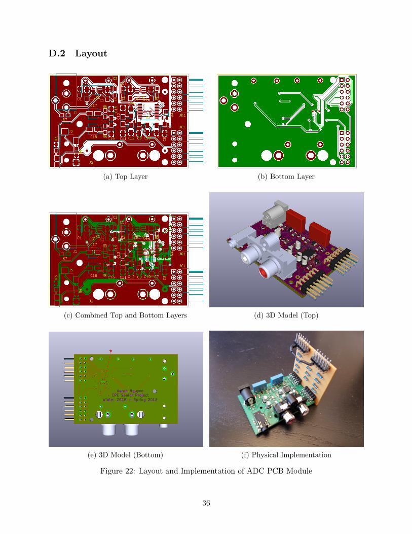
D.2 Layout
(a) Top Layer (b) Bottom Layer
(c) Combined Top and Bottom Layers (d) 3D Model (Top)
(e) 3D Model (Bottom) (f) Physical Implementation
Figure 22: Layout and Implementation of ADC PCB Module
36

E VHDL Source Code
Listing 1: System Wrapper Codelibrary IEEE;use IEEE.STD_LOGIC_1164.ALL;
entity wrapper_filter_system is5 Port (
−− Main InputsCLK_FPGA : in STD_LOGIC;CPU_RESETN : in STD_LOGIC;
10 −− Debugging Output−− DB_CLK_MASTER_ADC : out STD_LOGIC; −− JB1, System Clock for ADC (24.576 MHz)−− DB_CLK_LRCK_ADC : out STD_LOGIC; −− JB2, Channel Select for ADC (96 kHz)−− DB_CLK_BCK_ADC : out STD_LOGIC; −− JB3, Bit Clock for ADC (6.144 MHz)−− DB_ADC_DOUT : out STD_LOGIC; −− JB4, Data Input to FPGA (from ADC
15 −− DB_CLK_MASTER_DAC : out STD_LOGIC; −− JB7, System Clock for DAC (24.576 MHz)−− DB_CLK_LRCK_DAC : out STD_LOGIC; −− JB8, Channel Select for DAC (96 kHz)−− DB_CLK_BCK_DAC : out STD_LOGIC; −− JB9, Bit Clock for DAC (6.144 MHz)−− DB_DAC_DOUT : out STD_LOGIC; −− JB10, Data Output to DAC
20 −− ADC − TI PCM1803ADC_DIN : in STD_LOGIC; −− JC7, labeled as DOUT in datasheetADC_BCK : out STD_LOGIC; −− JC8ADC_LRCK : out STD_LOGIC; −− JC9ADC_SCK : out STD_LOGIC; −− JC10
25ADC_FMT : out STD_LOGIC_VECTOR(1 downto 0); −− JD2 <FMT[1]>, JD1 <FMT[0]>ADC_MD : out STD_LOGIC_VECTOR(1 downto 0); −− JD4 <MD[1]>, JD3 <MD[0]>ADC_AL_PDWN : out STD_LOGIC; −− JD8ADC_BPAS : out STD_LOGIC; −− JD9
30 ADC_OSR : out STD_LOGIC; −− JD10
−− DAC − PMOD I2S from DigilentDAC_SCK : out STD_LOGIC; −− JA7, labeled as mclk in datasheetDAC_LRCK : out STD_LOGIC; −− JA8
35 DAC_BCK : out STD_LOGIC; −− JA9, labeled as SCK in data sheetDAC_SDOUT : out STD_LOGIC; −− JA10, labeled as SDIN in data sheet
−− FILTER (internal)FILTER_ENABLE : in STD_LOGIC; −− SW[0], LED[0]
40 FILTER_ENABLE_LED : out STD_LOGIC);
end wrapper_filter_system;
architecture Behavioral of wrapper_filter_system is45 constant C_DATA_WIDTH : integer := 24;
constant C_NUM_COEFFS : integer := 9;constant C_SCALAR : integer := 512;
component clk_wiz_050 port ( −− Clock in ports
CLK_IN : in STD_LOGIC;−− Clock out portsMCLK : out STD_LOGIC;CLK_BCK : out STD_LOGIC;
55 −− Status and control signalsreset : in STD_LOGIC;locked : out STD_LOGIC
);end component;
60component clocks
generic ( G_LRCK_COUNT : integer := 64/2); −− 6.144 MHz / 64 = 96000Port ( RESET : in STD_LOGIC := '0';
37

CLK_IN : in STD_LOGIC := '0'; −− 24.576 MHz65 CLK_BCK_IN : in STD_LOGIC := '0'; −− 6.144 MHz
UNLOCKED : in STD_LOGIC := '0'; −− active highOUT_CLK_LRCK_DOUBLE : out STD_LOGIC := '0'; −− 192 kHzOUT_CLK_LRCK_ADC : out STD_LOGIC := '0'; −− 96 kHzOUT_CLK_LRCK_DAC : out STD_LOGIC := '0'); −− 96 kHz
70 end component;
component adc_driverPort (
UNLOCKED: in STD_LOGIC;75 RESET : in STD_LOGIC;
SCK_IN : in STD_LOGIC; −− 24.576 MHzLRCK_IN : in STD_LOGIC; −− 96kHzBCK_IN : in STD_LOGIC; −− 6.144MHzDIN : in STD_LOGIC;
80 MD : out STD_LOGIC_VECTOR(1 downto 0); −− 0,0FMT : out STD_LOGIC_VECTOR(1 downto 0); −− 0,1OSR : out STD_LOGIC; −− low −− 64x osr delta sigmaBPAS : out STD_LOGIC; −− low − bypass so no dc in doutAL_PDWN : out STD_LOGIC; −− high
85 GOOD : out STD_LOGIC; −− to processorDOUT : out STD_LOGIC_VECTOR(23 downto 0)
);end component;
90 component filter_drivergeneric (
G_DATA_WIDTH : integer := 24;G_NUM_COEFFS : integer := 9;G_SCALAR : integer := 512
95 );port (
MCLK : in STD_LOGIC; −− MCLK (24.576MHz). Must be syncedENABLE : in STD_LOGIC;ENABLE_LED : out STD_LOGIC;
100 GOOD : in STD_LOGIC;DIN : in STD_LOGIC_VECTOR (G_DATA_WIDTH -1 downto 0);DOUT : out STD_LOGIC_VECTOR (G_DATA_WIDTH -1 downto 0)
);end component;
105component dac_driver
Port ( RESET : in STD_LOGIC;UNLOCKED : in STD_LOGIC;SCK_IN : in STD_LOGIC;
110 LRCK_IN : in STD_LOGIC;BCK_IN : in STD_LOGIC;SDIN : in STD_LOGIC_VECTOR(23 downto 0);SDOUT : out STD_LOGIC
);115 end component;
signal s_reset : STD_LOGIC := '0';signal s_mclk : STD_LOGIC := '0'; −− 24.576 MHzsignal s_clk_bck : STD_LOGIC := '0'; −− 6.144 MHz
120 signal s_unlocked : STD_LOGIC := '0';
signal s_clk_lrck_double : STD_LOGIC := '0';signal s_clk_lrck_adc : STD_LOGIC := '0';signal s_clk_lrck_dac : STD_LOGIC := '0';
125signal s_good : STD_LOGIC := '0';signal s_adc_dout : STD_LOGIC_VECTOR(C_DATA_WIDTH -1 downto 0) := (others => '0');signal s_filter_dout : STD_LOGIC_VECTOR(C_DATA_WIDTH -1 downto 0) := (others => '0');signal s_dac_dout : STD_LOGIC := '0';
130begin
38

MAIN_CLOCK: clk_wiz_0Port map (
CLK_IN => CLK_FPGA,135 MCLK => s_mclk,
CLK_BCK => s_clk_bck,reset => s_reset,locked => s_unlocked
);140
CLOCK_SYSTEM: clocksgeneric map (
G_LRCK_COUNT => 64/2)
145 port map (RESET => s_reset,CLK_IN => s_mclk,CLK_BCK_IN => s_clk_bck,UNLOCKED => s_unlocked,
150 OUT_CLK_LRCK_DOUBLE => s_clk_lrck_double,OUT_CLK_LRCK_ADC => s_clk_lrck_adc,OUT_CLK_LRCK_DAC => s_clk_lrck_dac
);
155 ADC_SYSTEM: adc_driverport map (
UNLOCKED => s_unlocked,RESET => s_reset,SCK_IN => s_mclk,
160 LRCK_IN => s_clk_lrck_double,BCK_IN => s_clk_bck,DIN => ADC_DIN,MD => ADC_MD,FMT => ADC_FMT,
165 OSR => ADC_OSR,BPAS => ADC_BPAS,AL_PDWN => ADC_AL_PDWN,GOOD => s_good,DOUT => s_adc_dout
170 );
FILTER_SYSTEM: filter_drivergeneric map (
G_DATA_WIDTH => C_DATA_WIDTH,175 G_NUM_COEFFS => C_NUM_COEFFS,
G_SCALAR => C_SCALAR)
port map (MCLK => s_mclk, −− MCLK (24.576MHz). Must be synced
180 ENABLE => FILTER_ENABLE,ENABLE_LED => FILTER_ENABLE_LED,GOOD => s_good,DIN => s_adc_dout,DOUT => s_filter_dout
185 );
DAC_SYSTEM: dac_driverport map (
RESET => s_reset,190 UNLOCKED => s_unlocked,
SCK_IN => s_mclk,LRCK_IN => s_clk_lrck_double,BCK_IN => s_clk_bck,SDIN => s_filter_dout, −− VECTOR OUTPUT TO DAC
195 SDOUT => DAC_SDOUT −− ACTUAL OUTPUT TO DAC);
s_reset <= not CPU_RESETN; −− RESET is inverted on board
39

200 −− DB_CLK_MASTER_ADC <= s_clk_master_adc;−− DB_CLK_MASTER_DAC <= s_clk_master_dac;−− DB_CLK_LRCK_ADC <= s_clk_lrck_adc;−− DB_CLK_LRCK_DAC <= s_clk_lrck_dac;−− DB_CLK_BCK_ADC <= s_clk_bck_adc;
205 −− DB_CLK_BCK_DAC <= s_clk_bck_dac;−− DB_ADC_DOUT <= ADC_DIN;−− DB_DAC_DOUT <= s_dac_dout;
ADC_SCK <= s_mclk;210 ADC_LRCK <= s_clk_lrck_adc;
ADC_BCK <= s_clk_bck;DAC_SCK <= s_mclk;DAC_LRCK <= s_clk_lrck_dac;DAC_BCK <= s_clk_bck;
215end Behavioral;
Listing 2: Clock Driverlibrary IEEE;use IEEE.STD_LOGIC_1164.ALL;use IEEE.NUMERIC_STD.ALL;
5 entity clocks isgeneric ( G_LRCK_COUNT : integer := 64/2); −− 6.144 MHz / 64 = 96000Port ( RESET : in STD_LOGIC := '0';
CLK_IN : in STD_LOGIC := '0'; −− 24.576 MHzCLK_BCK_IN : in STD_LOGIC := '0'; −− 6.144 MHz
10 UNLOCKED : in STD_LOGIC := '0'; −− active highOUT_CLK_LRCK_DOUBLE : out STD_LOGIC := '0'; −− 192 kHzOUT_CLK_LRCK_ADC : out STD_LOGIC := '0'; −− 96 kHzOUT_CLK_LRCK_DAC : out STD_LOGIC := '0'); −− 96 kHz
end clocks;15
architecture Behavioral of clocks issignal s_clk_lrck_adc : STD_LOGIC := '0';signal s_clk_lrck_dac : STD_LOGIC := '0';signal s_clk_bck_adc : STD_LOGIC := '0';
20 signal s_clk_bck_dac : STD_LOGIC := '0';signal s_clk_lrck_double : STD_LOGIC := '0';
beginADC_LRCK: process(RESET, CLK_BCK_IN)
−− 6.144 MHz / 64 = 9600025 variable v_adc_lrck_count : integer range 0 to G_LRCK_COUNT := 0;
beginif (RESET = '1') then
s_clk_lrck_adc <= '0';v_adc_lrck_count := 0;
30 elsif (falling_edge(CLK_BCK_IN)) thenif (v_adc_lrck_count = G_LRCK_COUNT) then
s_clk_lrck_adc <= not s_clk_lrck_adc;v_adc_lrck_count := 0;
end if;35 v_adc_lrck_count := v_adc_lrck_count + 1;
end if;end process ADC_LRCK;
DAC_LRCK: process(RESET, CLK_BCK_IN)40 −− 6.144 MHZ / 64 = 96000
variable v_dac_lrck_count : integer range 0 to G_LRCK_COUNT;begin
if (RESET = '1') thens_clk_lrck_dac <= '0';
45 v_dac_lrck_count := 0;elsif (falling_edge(CLK_BCK_IN)) then
if (v_dac_lrck_count = G_LRCK_COUNT) then
40

s_clk_lrck_dac <= not s_clk_lrck_dac;v_dac_lrck_count := 0;
50 end if;v_dac_lrck_count := v_dac_lrck_count + 1;
end if;end process DAC_LRCK;
55 −− This clock is used to trigger on each falling edge of a channel switch.DOUBLE_LRCK: process(RESET, CLK_BCK_IN)
−− 6.144 MHz / 32 = 192000variable v_double_lrck_count : integer range 0 to G_LRCK_COUNT/2 := 0;
begin60 if (RESET = '1') then
s_clk_lrck_double <= '0';v_double_lrck_count := 0;
elsif (falling_edge(CLK_BCK_IN)) thenif (v_double_lrck_count = G_LRCK_COUNT/2) then
65 s_clk_lrck_double <= not s_clk_lrck_double;v_double_lrck_count := 0;
end if;v_double_lrck_count := v_double_lrck_count + 1;
end if;70 end process DOUBLE_LRCK;
OUT_CLK_LRCK_ADC <= s_clk_lrck_adc when (RESET = '0' and UNLOCKED = '1') else '0';OUT_CLK_LRCK_DAC <= not s_clk_lrck_dac when (RESET = '0' and UNLOCKED = '1') else '0';OUT_CLK_LRCK_DOUBLE <= s_clk_lrck_double when (RESET = '0' and UNLOCKED = '1') else '0';
75 end Behavioral;
Listing 3: ADC Driverlibrary IEEE;use IEEE.STD_LOGIC_1164.ALL;
entity adc_driver is5 Port (
UNLOCKED: in STD_LOGIC; −− from clockwiz, unusedRESET : in STD_LOGIC;SCK_IN : in STD_LOGIC; −− 24.576 MHzLRCK_IN : in STD_LOGIC; −− 192kHz
10 BCK_IN : in STD_LOGIC; −− 6.144MHzDIN : in STD_LOGIC;MD : out STD_LOGIC_VECTOR(1 downto 0); −− 0,0FMT : out STD_LOGIC_VECTOR(1 downto 0); −− 0,1OSR : out STD_LOGIC; −− low −− 64x osr delta sigma
15 BPAS : out STD_LOGIC; −− low − bypass so no dc in doutAL_PDWN : out STD_LOGIC; −− highGOOD : out STD_LOGIC; −− to processorDOUT : out STD_LOGIC_VECTOR(23 downto 0)
);20 end adc_driver;
architecture Behavioral of adc_driver issignal s_good : STD_LOGIC := '0';signal s_dout : STD_LOGIC_VECTOR(23 downto 0) := (others => '0');
25 signal s_ready_adc : boolean := FALSE;signal s_used_lrck : boolean := FALSE;signal s_dout_index : integer range -1 to 23 := -1;signal s_din : STD_LOGIC;
begin30 −− 192 kHz rate, fs is at 96kHz => triggers on every channel switch’s
−− falling edgeLRCK_TRIGGER: process(RESET, LRCK_IN, s_used_lrck)begin
if (RESET = '1') then35 s_ready_adc <= FALSE;
else
41

if (falling_edge(LRCK_IN)) thens_ready_adc <= TRUE;
end if;40 if (s_used_lrck) then
s_ready_adc <= FALSE;end if;
end if;end process;
45−− output of ADC (input to FPGA)CLOCK_OUTPUT: process(RESET, BCK_IN, s_ready_adc)
variable v_dout_index : integer range -1 to 23 := -1;begin
50 if (RESET = '1') thens_good <= '0';v_dout_index := -1;s_dout <= (others => '0');
elsif (falling_edge(BCK_IN)) then55 if (s_ready_adc) then
s_good <= '0';v_dout_index := 23;s_dout(22 downto 0) <= (others => '0');s_used_lrck <= TRUE;
60 end if;if (v_dout_index > -1) then
s_dout(v_dout_index) <= DIN;v_dout_index := v_dout_index - 1;
else65 s_good <= '1';
s_used_lrck <= FALSE;end if;
end if;end process;
70MD <= "00" when (RESET = '0') else "ZZ";FMT <= "01" when (RESET = '0') else "ZZ";OSR <= '0' when (RESET = '0') else 'Z';BPAS <= '0' when (RESET = '0') else 'Z';
75 AL_PDWN <= '1' when (RESET = '0') else '0';GOOD <= s_good when (RESET = '0') else '0';DOUT <= s_dout;
end Behavioral;
Listing 4: Filter Driverlibrary IEEE;use IEEE.STD_LOGIC_1164.ALL;use IEEE.NUMERIC_STD.ALL;
5 entity filter_driver isgeneric (
G_DATA_WIDTH : integer := 24;G_NUM_COEFFS : integer := 9;G_SCALAR : integer := 512
10 );Port (
MCLK : in STD_LOGIC; −− MCLK (24.576MHz). Must be syncedENABLE : in STD_LOGIC;ENABLE_LED : out STD_LOGIC;
15 GOOD : in STD_LOGIC;DIN : in STD_LOGIC_VECTOR (G_DATA_WIDTH -1 downto 0);DOUT : out STD_LOGIC_VECTOR (G_DATA_WIDTH -1 downto 0)
);end filter_driver;
20architecture Behavioral of filter_driver is
−− function source: https://groups.google.com/forum/#!topic/comp.lang.vhdl/sG3bWafr41c
42

function f_log2(input:integer) return integer isvariable v_temp : integer;
25 variable v_log : integer;begin
v_temp := input;v_log := 0;while (v_temp /= 0) loop
30 v_temp := v_temp / 2;v_log := v_log + 1;end loop;
return v_log;end function f_log2;
35type xn_array is array (0 to 2**(f_log2(G_NUM_COEFFS))-1) of signed(G_DATA_WIDTH downto 0);type n_array is array (0 to 2**(f_log2(G_NUM_COEFFS))-1) of signed(G_DATA_WIDTH downto 0);type bk_coeffs is array (0 to 2**(f_log2(G_NUM_COEFFS))-1) of signed(17 downto 0);
40 constant C_LIMIT_LOW : signed(G_DATA_WIDTH -1 downto 0):= to_signed(-( 2**( G_DATA_WIDTH -1 ) ), G_DATA_WIDTH);
constant C_LIMIT_HIGH : signed(G_DATA_WIDTH -1 downto 0):= to_signed(2**( G_DATA_WIDTH -1 )-1, G_DATA_WIDTH);
constant C_LOG_SCALAR : integer := f_log2(G_SCALAR);45
−− multiply all coeffs by G_SCALAR and put into romconstant ROM_COEFFS : bk_coeffs :=( −− 9 tap moving average filter
−− y[n] = 512 ∗ 0.111(x[n] + x[n−1] + ... + x[n−8])50 0 => to_signed(56, 18),
1 => to_signed(56, 18),2 => to_signed(56, 18),3 => to_signed(56, 18),4 => to_signed(56, 18),
55 5 => to_signed(56, 18),6 => to_signed(56, 18),7 => to_signed(56, 18),8 => to_signed(56, 18),others => (others => '0')
60 );
signal xn : xn_array := (others => (others => '0'));signal yn : signed(48 downto 0) := (others => '0');signal s_processed : STD_LOGIC := '0';
65 signal s_wait_next_cycle : boolean := FALSE;signal s_negative : STD_LOGIC := '0';
attribute use_dsp : string;attribute use_dsp of yn : signal is "yes";
70 begin−−−− This one is slower than FILTER2 since it computes each coefficient output at every clock edge.−− FILTER: process(MCLK, GOOD, DIN, s_processed, s_wait_next_cycle)−− variable v_i : integer range 0 to G_NUM_COEFFS−1;−− constant v_i_mid : integer := (G_NUM_COEFFS−1)/2;
75 −− begin−− if (rising_edge(MCLK)) then−− if (GOOD = ’1’) then−− if (s_wait_next_cycle = TRUE) then−− for i in G_NUM_COEFFS−1 downto 1 loop
80 −− xn(i) <= xn(i−1);−− end loop;−− xn(0) <= signed(’0’ & DIN);−− yn <= (others => ’0’);−− v_i := 0;
85 −− s_processed <= ’0’;−− s_wait_next_cycle <= FALSE;−− report "Rising Edge GOOD Processed";−− elsif (v_i < v_i_mid) then −− goes up to one before middle if odd num coeffs−− yn <= yn + resize(ROM_COEFFS(v_i) ∗ ( xn(v_i) + xn(G_NUM_COEFFS−1−v_i) ), 48);
90 −− v_i := v_i + 1;
43

−− elsif (G_NUM_COEFFS mod 2 = 1 and v_i = v_i_mid) then −− odd case−− yn <= yn + resize(( ROM_COEFFS(v_i) ∗ xn(v_i) ),48);−− v_i := v_i + 1;−− elsif (v_i > v_i_mid) then −− logic delays output one clock cycle
95 −− s_processed <= ’1’;−− end if;−− else −− GOOD = ’0’−− s_wait_next_cycle <= TRUE;−− end if;
100 −− end if;−− end process;
−− filters data in 2 cyclesFILTER2: process(MCLK, GOOD, DIN, s_processed, s_wait_next_cycle)
105 constant v_i_mid : integer := (G_NUM_COEFFS -1)/2;variable v_yn : signed(48 downto 0) := (others => '0');
beginif (rising_edge(MCLK)) then
if (GOOD = '1') then110 if (s_wait_next_cycle = TRUE) then
for i in G_NUM_COEFFS -1 downto 1 loopxn(i) <= xn(i-1);
end loop;xn(0) <= signed('0' & DIN);
115 v_yn := (others => '0');s_processed <= '0';s_wait_next_cycle <= FALSE;report "Rising Edge GOOD Processed";
elsif (s_processed = '0') then −− goes up to one before middle if odd num coeffs120 for i in 0 to v_i_mid-1 loop
v_yn := v_yn + resize(ROM_COEFFS(i) * ( xn(i) + xn(G_NUM_COEFFS -1-i) ), 48);end loop;if (G_NUM_COEFFS mod 2 = 1) then
v_yn := v_yn + resize(ROM_COEFFS(v_i_mid) * xn(v_i_mid), 48);125 end if;
yn <= v_yn;s_processed <= '1';
end if;else −− GOOD = ’0’
130 s_wait_next_cycle <= TRUE;end if;
end if;end process;
135 −−−− Attempted an overflow fix via a process b ut didn’t work. Kept for reference.−− TRUNCATE: process(s_processed)−− variable yn_shifted : signed(48 downto 0) := (others => ’0’);−− begin−− if (rising_edge(s_processed)) then
140 −− yn_shifted := shift_right(yn, C_LOG_SCALAR);−− report "yn_shifted: " & integer’image(to_integer(yn_shifted));−− if (yn_shifted <= C_LIMIT_LOW) then−− report "C_LIMIT_LOW: " & integer’image(to_integer(C_LIMIT_LOW));−− yn_truncated <= std_logic_vector(C_LIMIT_LOW);
145 −− elsif (yn_shifted >= C_LIMIT_HIGH) then−− report "C_LIMIT_HIGH: " & integer’image(to_integer(C_LIMIT_HIGH));−− yn_truncated <= std_logic_vector(C_LIMIT_HIGH);−− else−− yn_truncated <=yn_shifted(48)&std_logic_vector(yn_shifted(G_DATA_WIDTH−2 downto 0));
150 −− end if;−− end if;−− end process;
DOUT <= std_logic_vector(yn(G_DATA_WIDTH -1+C_LOG_SCALAR downto C_LOG_SCALAR)) when155 (ENABLE = '1' and s_processed = '1') else DIN when (ENABLE = '0');
ENABLE_LED <= ENABLE;end Behavioral;
44

Listing 5: DAC Driverlibrary IEEE;use IEEE.STD_LOGIC_1164.ALL;
entity dac_driver is5 Port ( RESET : in STD_LOGIC;
UNLOCKED : in STD_LOGIC;SCK_IN : in STD_LOGIC;LRCK_IN : in STD_LOGIC;BCK_IN : in STD_LOGIC;
10 SDIN : in STD_LOGIC_VECTOR(23 downto 0);SDOUT : out STD_LOGIC
);end dac_driver;
15 architecture Behavioral of dac_driver issignal s_sdout : STD_LOGIC := '0';signal s_used_lrck : boolean := FALSE;signal s_ready : boolean := FALSE;
begin20 LRCK_TRIGGER: process(RESET, LRCK_IN, s_used_lrck)
beginif (RESET = '1') then
s_ready <= FALSE;else
25 if (falling_edge(LRCK_IN)) thens_ready <= TRUE;
end if;if (s_used_lrck) then
s_ready <= FALSE;30 end if;
end if;end process;
CLOCK_OUT_SAMPLES: process(RESET, BCK_IN, s_ready)35 variable v_out_index : integer range -1 to 23 := -1;
variable v_sdin : STD_LOGIC_VECTOR(23 downto 0);begin
if (RESET = '1') thenv_sdin := (others => '0');
40 s_sdout <= '0';v_out_index := -1;
elsif (falling_edge(BCK_IN)) thenif (s_ready) then
v_out_index := 23;45 v_sdin := SDIN;
s_used_lrck <= TRUE;end if;if (v_out_index > -1) then
s_sdout <= v_sdin(v_out_index);50 v_out_index := v_out_index - 1;
else −− donev_sdin := (others => '0');s_sdout <= '0';s_used_lrck <= FALSE;
55 end if;end if;
end process;
SDOUT <= s_sdout;60 end Behavioral;
45