impact off micro and nanotechnology (mnt) to basque industry · nanopowder ceramics and...
TRANSCRIPT

© TEMAS AG: 1 31.5.05
TEMAS Technologie Treuhand
Impact off Micro and Nanotechnology (MNT)
to Basque Industry
Karl HöhenerTechnology Advisor
TEMAS AGTechnologie Treuhand

© TEMAS AG: 2 31.5.05
TEMAS Technologie Treuhand
Micro- and NanoTechMethods and Results from Switzerland
4 Introduction4 Nanotechnologies in
Switzerland an overview4 Benefits for the
automotive sector through the use of MNT
4 Benefits for the Machine Tool Industry
4 Instrumentation and Nano-Systems
4 Outlook

© TEMAS AG: 3 31.5.05
TEMAS Technologie Treuhand
TEMAS Ltd.The Innovation Company
Service provider along the Innovation-Path
Technology ManagementTo suppot Funding- and Innovation Agencies
Concepts to strengthen the economic impactof new technologies (How to address SMEs, programme design, …)Advice for implementation and impact controlling of programmes on a regional or national levelIndependent evaluation of projects, risks, …
Technology TrusteeTo support Companies
Impact of new Technologies to the product portfolio

© TEMAS AG: 4 31.5.05
TEMAS Technologie Treuhand
TEMAS Technology Impulse®Impulses for your innovation process; increased customer benefit through new functionalities for existing or new products.
The TEMAS Technology Impulse supports you in generating added value.
TEMAS Technology Flash®Show added value, tight core competencies, and recognize degrees of maturity by accurate analysis of your technology portfolio.
The TEMAS Technology Flash gives you security for your decision processes.
TEMAS Technology Scout®With the TEMAS Technology Scout you will find the best suited experts and partners for your specific requirements.
The TEMAS Technology Scout supports you in shortening your development times and costs.
TEMAS Technology CoachingSecure achievement of project objectives by active accompaniment and coaching of your team, timely and within budget.
With the TEMAS Technology Coaching you will reach your goal safely.
providing services along the Innovation-Path
TEMAS Profiler®Selects the most attractive application fields using the TEMAS Profiler to set the right priorities.
TEMAS Technology Scout® BusinessWith the TEMAS Technology Scout Business you find the best partner in order to commercialize your technology, technology-oriented products, or services in the high tech sector.
The TEMAS Technology Scout Business is your door-opener to the Swiss market.
To support companies

© TEMAS AG: 5 31.5.05
TEMAS Technologie Treuhand
Success stories from Switzerland
4 Introduction4 Nanotechnologies in Switzerland an overview4 Benefits for the automotive sector through
the use of MNT4 Benefits for the Machine Tool Industry4 Instrumentation and Nano-Systems4 Outlook

© TEMAS AG: 6 31.5.05
TEMAS Technologie Treuhand
Nano scale science began 1981 in the IBM's Zurich Research Laboratory with the groundbreaking invention of the scanning tunneling microscope
(STM), for which Gerd Binnig and Heinrich Rohrer were awarded the Nobel Prize for Physics in 1986.
Nano Scale Science in Switzerland

© TEMAS AG: 7 31.5.05
TEMAS Technologie Treuhand
Nanotechnology, why Switzerland is leading
Comparison of scales:STM: Atom Scanning Ping-Pong-ball
and Matterhorn
to to

© TEMAS AG: 8 31.5.05
TEMAS Technologie Treuhand
Quelle: Nach VDI
0.1nmTime
Applications :Smart Materials
OpticBiology
CommunicationSensors
Applications of Nano-Technology
0.1mm
0.1µm
Biology
Physics
Chemistry
MACRO
MICRO
NANO
SurfacesStructures
SensorsBio chips
Powders, CNT...
Structural size
Supra Molecular -Chemistry
Cell biology
FunctionalMolecule Design
Molecular biology
ComplexChemistry
Quantum effects
Material design
Micro -Electronics
Electronics
Electro -Technology
Source: VDI
Macro - Micro – Nano - Scale
Definition

© TEMAS AG: 9 31.5.05
TEMAS Technologie Treuhand
New scientific findings will be available continuously
Maturity
TimeInvention leader
EarlyFollower Late Follower
DominantDesign
Inventors
SME
Innovation leader
Worldmarketleaders
Companies
Nano projects links:• Scientists, • Technologists and• Engineersto create a “NANOMETER“business sector
NANOprojects
new
new
new
Curr.status
Applications
Techn
ologie
s
Scie
ntifi
cFi
ndin
gs
The NANO-Technology starts developing

© TEMAS AG: 10 31.5.05
TEMAS Technologie Treuhand
Implementation: Clusters of Competence

© TEMAS AG: 11 31.5.05
TEMAS Technologie Treuhand
Copyright Management Team TOP NANO 21
First Structure of Swiss Nano Business Sector

© TEMAS AG: 12 31.5.05
TEMAS Technologie Treuhand
The Swiss NANO-Region
Industries around research centres
Companies applying Nanotechnologies
Research centres
Universitéde Genève
Universität Basel
PSIUniversitätSt.Gallen
EMPA St. Gallen
FH Buchs
SUPSI
EPFLEMPA Thun
Universitéde Neuchâtel
CSEMUniversitéde Fribourg
FH Biel
CSEM Alpnach
EMPA Dübendorf
ETHZ
FH Wallis
Metas
CAFI
FH Basel
IBM ResearchDivision
Companies applying Microtechnologies
Source: TOP NANO 21 & CTI
400 Km
20
0 K
m

© TEMAS AG: 13 31.5.05
TEMAS Technologie Treuhand
Success stories from Switzerland
4 Introduction4 Nanotechnologies in Switzerland an overview4 Benefits for the automotive sector through
the use of MNT4 Benefits for the Machine Tool Industry4 Instrumentation and Nano-Systems4 Outlook

© TEMAS AG: 14 31.5.05
TEMAS Technologie Treuhand
Benefits for the automotive sector through the use of MNT
4 New efficient diesel gas sensors combining nanopowder ceramics and micromachined silicon dice.
4 Self Cleaning Paints and Composites Containing Nanocrystalline Photocatalysts.
4 Dendritic Polymers for Nanostructured Composite Materials, new trend to fire retardancy weight reduction with Star Branch Polymer and clays.

© TEMAS AG: 15 31.5.05
TEMAS Technologie Treuhand
New Efficient Diesel Gas Sensors
Sensitive layerMetal lines
SiO2 Micro heater plate
MembraneSilicon substrate
Gas semiconductor sensors based on silicon technology
Combining Nanopowder Ceramics and Micro machined Silicon Dice
Source: EPFL

© TEMAS AG: 16 31.5.05
TEMAS Technologie Treuhand
Benefits for the automotive sector through the use of MNT
4 New efficient diesel gas sensors combining nanopowder ceramics and micromachined silicon dice.
4 Self Cleaning Paints and Composites Containing Nanocrystalline Photocatalysts.
4 Dendritic Polymers for Nanostructured Composite Materials, new trend to fire retardancy weight reduction with Star Branch Polymer and clays.

© TEMAS AG: 17 31.5.05
TEMAS Technologie Treuhand
Nature guides the solutionThe LOTUS effect
Source: http://www.botanik.uni-bonn.de
Nanotechnologie
Introduction

© TEMAS AG: 18 31.5.05
TEMAS Technologie Treuhand
The mystery of the LOTUS - effect
Source: http://www.botanik.uni-bonn.deREM pictures
Nanotechnologie
Introduction

© TEMAS AG: 19 31.5.05
TEMAS Technologie Treuhand
Source: DaimlerChrysler AG
Dank hohem Vernetzungs-grad ist der Klarlack besonders kratzfest
New self cleaning paints
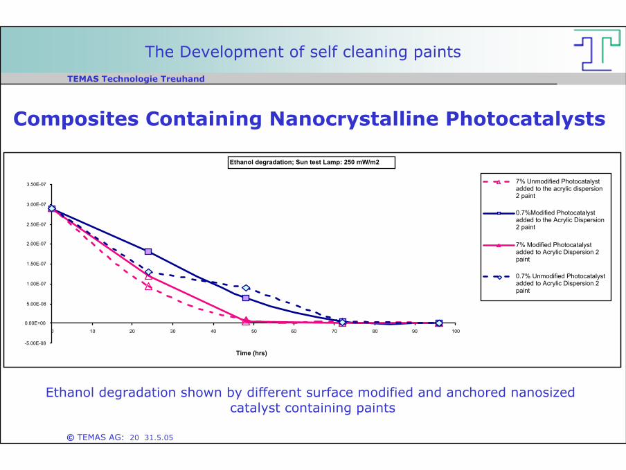
© TEMAS AG: 20 31.5.05
TEMAS Technologie Treuhand
The Development of self cleaning paints
.Ethanol degradation; Sun test Lamp: 250 mW/m2
-5.00E-08
0.00E+00
5.00E-08
1.00E-07
1.50E-07
2.00E-07
2.50E-07
3.00E-07
3.50E-07
0 10 20 30 40 50 60 70 80 90 100
Time (hrs)
7% Unmodified Photocatalystadded to the acrylic dispersion2 paint
0.7%Modified Photocatalystadded to the Acrylic Dispersion2 paint
7% Modified Photocatalystadded to Acrylic Dispersion 2paint
0.7% Unmodified Photocatalystadded to Acrylic Dispersion 2paint
Ethanol degradation shown by different surface modified and anchored nanosizedcatalyst containing paints
Composites Containing Nanocrystalline Photocatalysts

© TEMAS AG: 21 31.5.05
TEMAS Technologie Treuhand
Benefits for the automotive sector through the use of MNT
4 New efficient diesel gas sensors combining nanopowder ceramics and micromachined silicon dice.
4 Self Cleaning Paints and Composites Containing Nanocrystalline Photocatalysts.
4 Dendritic Polymers for Nanostructured Composite Materials, new trend to fire retardancy weight reduction with Star Branch Polymer and clays.
© TEMAS AG: 22 31.5.05
TEMAS Technologie Treuhand
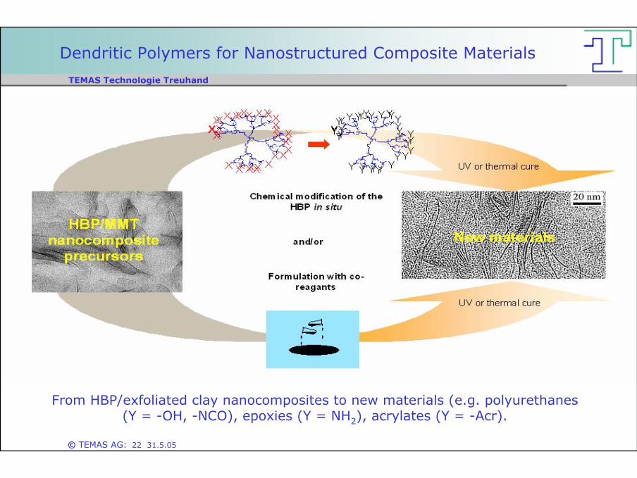
Dendritic Polymers for Nanostructured Composite Materials
From HBP/exfoliated clay nanocomposites to new materials (e.g. polyurethanes (Y = -OH, -NCO), epoxies (Y = NH2), acrylates (Y = -Acr).

© TEMAS AG: 23 31.5.05
TEMAS Technologie Treuhand
TEM micrographs of unexfoliated and exfoliated polyurethane nanocomposites along with the relative stiffness measured in the rubber plateau regime (plateau modulus normalized with respect to that of the same formulation without clay) as a function of the clay content, f, in weight %.
Dendritic Polymers for Nanostructured Composite Materials

© TEMAS AG: 24 31.5.05
TEMAS Technologie Treuhand
Success stories from Switzerland
4 Introduction4 Nanotechnologies in Switzerland an overview4 Benefits for the automotive sector through
the use of MNT4 Benefits for the Machine Tool Industry4 Instrumentation and Nano-Systems4 Outlook

© TEMAS AG: 25 31.5.05
TEMAS Technologie Treuhand
Benefits for the Machine Tool Industry
4 Ultra high precision systems for machining and assembly.
4 Nano indentation to analyse tools, hard coatings and wear resistance.
4 3-D touch probe with 5 nm resolution and 20 nm repeatability for coordinate measuring machines.

© TEMAS AG: 26 31.5.05
TEMAS Technologie Treuhand
The Delta Cube II:mechanical structureof the new designedmicro-EDM machine
Linar table of Delta Cube II:• 10 mm movement, • 10 nm resolution
Nanofactory

© TEMAS AG: 27 31.5.05
TEMAS Technologie Treuhand
from CAD design
to prototype
Presentation of the Sigma 6 robot
Ultra high precision parallel manipulator family with 3 to 6 degrees of freedom
Nanofactory

© TEMAS AG: 28 31.5.05
TEMAS Technologie Treuhand
Three-axis machine and milling tool
Ultrasonically assisted high speed nano-micro milling

© TEMAS AG: 29 31.5.05
TEMAS Technologie Treuhand
AWM Werkzeugbau AG
Nano Replication

© TEMAS AG: 30 31.5.05
TEMAS Technologie Treuhand
Benefits for the Machine Tool Industry
4 Ultra high precision systems for machining and assembly.
4 Nano indentation to analyse tools hard coatings and wear resistance.
4 3-D touch probe with 5 nm resolution and 20 nm repeatability for coordinate measuring machines.

© TEMAS AG: 31 31.5.05
TEMAS Technologie Treuhand
Example of nanoindentation in TiAlSiN multilayer thin film. a) load-displacement curves showing discontinuities due to the formation of nano
and micro scale cracks. b) AFM micrograph showing crack morphology of an indent.
Nanoindentation for mechanical properties and fracture of nanostructured materials
0
500
1000
1500
2000
2500
3000
500 1000 1500 2000 2500 3000
Load
On
Sam
ple
[mN
]
Displacement Into Surface [nm]
B - 225
Nanoindentation

© TEMAS AG: 32 31.5.05
TEMAS Technologie Treuhand
Atomistic simulation ofnanoindentation.a) zone beneath the indenter for
the single crystal sample at a displacement of 12.3 Angstrom,
b) for the 12 nm gain sample at a displacement of 11.9 Angstrom, only non FCC atoms are shown.
c) A view of the 5 nm average grain size sample at an indentation depth of 20 Angstrom. The yellow arrows signify relative motion of the gains relative to the center of mass of the yellow atoms.
Nanoindentation
Nanoindentation for mechanical properties and fracture of nanostructured materials

© TEMAS AG: 33 31.5.05
TEMAS Technologie Treuhand
Benefits for the Machine Tool Industry
4 Ultra high precision systems for machining and assembly.
4 Nano indentation to analyse tools hard coatings and wear resistance.
4 3-D touch probe with 5 nm resolution and 20 nm repeatability for coordinate measuring machines.

© TEMAS AG: 34 31.5.05
TEMAS Technologie Treuhand
sensor
probe
magnet
Kinematic structure of the 3D touch probe (left), magnetic holding of the probing element (centre) and mechanical filter (right).
The standard deviation of repeated measurements, e.g. the difference between left and right probing on a 5 mm gauge block, was in the order of 5 nm.
3D touch probe for coordinate measuring machines

© TEMAS AG: 35 31.5.05
TEMAS Technologie Treuhand
Success stories from Switzerland
4 Introduction4 Nanotechnologies in Switzerland an overview4 Benefits for the automotive sector through
the use of MNT4 Benefits for the Machine Tool Industry4 Instrumentation and Nano-Systems4 Outlook

© TEMAS AG: 36 31.5.05
TEMAS Technologie Treuhand
Instrumentation and Nano-Systems
4 Digital Holography for the Nano Scale,
4 New generation of atomic force microscopes with a new resolution/stroke range of SPM (AFM, STM) for applications in air and liquids,
4 Nanomanipulation of mesoscopic objects –new techniques and applications.New generation haptic devices for manipulation at the nano scale,

© TEMAS AG: 37 31.5.05
TEMAS Technologie Treuhand
Digital Holographic Microscopy (DHM) is a new instrument with up to 10 images a second.
The instrument is capable of imaging cells down to the nano- scale.
It was demonstrated to be very efficient in visualizing small deformations and movements of particles, vesicles and living cells, like neurons.
Resolutions of less than 40nm could be reached on the axis of the microscope.
Gold particles with diameters down to 20 nm could be
Digital Holography Microscopes (DHM)

© TEMAS AG: 38 31.5.05
TEMAS Technologie Treuhand
Material sciences
Micro optics quality control
Surface 3D topography
Bio- support nano structure Quality control of spots on biochips
Pollen recognition
without contrast agents
Research &Proof ofPrinciple
ProductDevelopment Prototyping Market
Introduction Production
Lyncée Tec SAThe Solution for Nano imaging
Digital Holography Microscopes (DHM)

© TEMAS AG: 39 31.5.05
TEMAS Technologie Treuhand
Instrumentation and Nano-Systems
4 Digital Holography for the Nano Scale,
4 New generation of atomic force microscopes with a new resolution/stroke range of SPM (AFM, STM) for applications in air and liquids,
4 Nanomanipulation of mesoscopic objects –new techniques and applications.New generation haptic devices for manipulation at the nano scale,

© TEMAS AG: 40 31.5.05
TEMAS Technologie Treuhand
Source: University of Basel
Nanotechnology – The dimension of the nanometer

© TEMAS AG: 41 31.5.05
TEMAS Technologie Treuhand
Microfabricated Cantilever made from silicon (Si)
40 µm
laserbeamdetector
sample
singleatomtip
scanning unitSource: University of Basel
Nanotechnology – Microscopy for the nanometer

© TEMAS AG: 42 31.5.05
TEMAS Technologie Treuhand
The scanning process („scanning“)
Nanotechnology – Microscopy for the nanometer
Source: University of Basel
© TEMAS AG: 43 31.5.05
TEMAS Technologie Treuhand
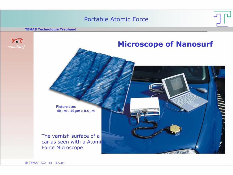
nanoSurf
The varnish surface of a car as seen with a AtomicForce Microscope
Picture size:40 µm × 40 µm × 0.4 µm
Microscope of Nanosurf
Portable Atomic Force

© TEMAS AG: 44 31.5.05
TEMAS Technologie Treuhand
Source: IBM
Cantilever sensorwithfunctionalised surface

© TEMAS AG: 45 31.5.05
TEMAS Technologie Treuhand
Source: IBM
ArtificialNose

© TEMAS AG: 46 31.5.05
TEMAS Technologie Treuhand
Cantisens® Research
• Microfabricated silicon levers with a thickness of 1 to 10 m
• Biochemical surface coating selectively binds specific target molecules.
• Adsorption of few molecules will create surface stress on the cantilever and result in tiny deflections of only a few nm
Research &Proof ofPrinciple
ProductDevelopment Prototyping Market
Introduction Production
Cantilever sensor platform
designed for:
industrial application
development and scientific research

© TEMAS AG: 47 31.5.05
TEMAS Technologie Treuhand
Instrumentation and Nano-Systems
4 Digital Holography for the Nano Scale,
4 New generation of atomic force microscopes with a new resolution/stroke range of SPM (AFM, STM) for applications in air and liquids, new cantilever sensors
4 Nanomanipulation of mesoscopic objects –new techniques and applications. New generation haptic devices for manipulation at the nano scale,

© TEMAS AG: 48 31.5.05
TEMAS Technologie Treuhand
Manipulation at the nanoscale with force feedback is made a accurate and easy through:
• A large workspace (∅300mm, which means a reduction factor of the order of 100'000),
• A force ranging from humansensitivity to 2.5kg.
Tip
Atomic Force Microscope
nanofeel
Nanomanipulation of mesoscopic objects –new techniques and applications

© TEMAS AG: 49 31.5.05
TEMAS Technologie Treuhand
Success stories from Switzerland
4 Introduction4 Nanotechnologies in Switzerland an overview4 Benefits for the automotive sector through
the use of MNT4 Benefits for the Machine Tool Industry4 Instrumentation and Nano-Systems4 Outlook

© TEMAS AG: 50 31.5.05
TEMAS Technologie Treuhand
Outlook
4 Safety and risk issues
4 Technology
4 Innovation Systems

© TEMAS AG: 51 31.5.05
TEMAS Technologie Treuhand
Introduction: Nano Safety and Risks
The implementation of nanotechnology poses unknown riskswhich are difficult to assess with respect to their impact on
- The environment- Human health- Ethical, legal and societal issues
Main source of unknowns:
Material properties can change on the nano scale!

© TEMAS AG: 52 31.5.05
TEMAS Technologie Treuhand
Impact on the environment
- Nanomaterials are already released into the environment
- Because of their small dimensions nanomaterials can be largely distributed within the environment in water streams, soil and air
- Like other chemicals nanomaterials can accumulate in the environment, but their effects are still unknown
- The persistence or degradation of nanomaterials in the environment is still unclear and can have enormous impacts

© TEMAS AG: 53 31.5.05
TEMAS Technologie Treuhand
Impact on human health
Nanomaterials can have a huge impact on human health:
- they can be absorbed in many ways by the human body (skin, lung, gastro-intestinal tract)
- They are distributed within the whole organism via blood and lymphatic systems
- They accumulate in organs (e.g. brain, kidney, liver)
- Because of their small size they can reach every place in the body

© TEMAS AG: 54 31.5.05
TEMAS Technologie Treuhand
Ethical, legal and societal implications
- Public perception of nanotechnology is a crucial determinant for its successful establishment as a future driving force in the economies worldwide
- As nanomaterials have different properties compared to the bulk materials new legislation and regulation will be necessary on an international level
- Ideas like toxic particles that can go everywhere and self-replicating nanorobots can produce fear and uncertainty in the broad public and can lead to severe societal problems

© TEMAS AG: 55 31.5.05
TEMAS Technologie Treuhand
- Optical Devices- Light Sources- Sensors- Energy Storage- Photovoltaics
Devices
Economic uncertainty
EnvironmentRisks
Societal Impacts
Toxicity
- Tips and Probes- Data Storage
Instrumentation
Economic uncertainty
EnvironmentRisks
Societal Impacts
Toxicity
- Machining- Self Assembly
Nanofactory/Replication
Economic uncertainty
EnvironmentRisks
Societal Impacts
Toxicity
- Biomaterials- Life Sciences
Nanobio/NanoMedicine
Economic uncertainty
EnvironmentRisks
Societal Impacts
Toxicity
- Novel Materials- Nano Particles- Surfaces
Materials/Powders
Economic uncertainty
EnvironmentRisks
Societal Impacts
Toxicity
No or little risks Medium risks High risks
Inherent risks of Nanotechnologies (a first overview)

© TEMAS AG: 56 31.5.05
TEMAS Technologie Treuhand
Outlook
4 Safety and risk issues
4 Technology
4 Innovation Systems

© TEMAS AG: 57 31.5.05
TEMAS Technologie Treuhand
Spontaneous self organization
4 Assembly of atoms and molecules without external influence to 2- and 3- dimensional structures is called self assembly.
4 Today this effect is mainly used to self assemble regular structures e.g. for wires, etc.
Outlook Technology

© TEMAS AG: 58 31.5.05
TEMAS Technologie Treuhand Nanotechnologie
Source: University of Basel
Spontaneous self organization

© TEMAS AG: 59 31.5.05
TEMAS Technologie Treuhand
Molecular 2D Solid-Gas Equilibrium
Nanotechnologie
G
C
S
S
Single molecule
C: 2D condensed phaseG: 2D gas phase S: step edges decorated
by molecules
Copyright University of Basel
Spontaneous self organization
© TEMAS AG: 60 31.5.05
TEMAS Technologie Treuhand
Outlook
4 Safety and risk issues
4 Technology
4 Collaboration Science and Economy– Knowledge and Technology Transfer– Education

© TEMAS AG: 61 31.5.05
TEMAS Technologie Treuhand
Knowledge and Technology Transfer
Productdevelopment
MarketTechnologydevelopment
Appliedresearch
Basicresearch
Knowledge orientedbasic research
Proactive object- orientedbasic research
Reactiveobject- orientedbasic research
Product- andprocess
developmentMarket
1
Market drivenKnowledge and
Technology Demand (KTD)
2Science drivenKnowledge and
Technology Transfer(KTT)
PUSH
PULL
The two-process approach KTT/KTD
© TEMAS AG: 62 31.5.05
TEMAS Technologie Treuhand
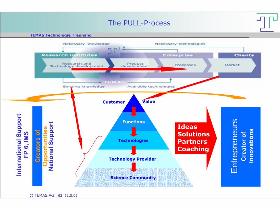
Customer Value
Functions
Entre
pren
eurs
Cre
ator
of
Inno
vatio
ns
Technologies
Technology Provider
Science Community
IdeasSolutionsPartnersCoaching
Cre
ator
s of
O
ppor
tuni
ties
Inte
rnat
iona
l Sup
port
FP 6
, IM
S
Nat
iona
l Sup
port
The PULL-Process

© TEMAS AG: 63 31.5.05
TEMAS Technologie Treuhand
Today
Productdevelopment
MarketTechnologydevelopment
Appliedresearch
Basicresearch
Knowledge orientedbasic research
Proactive object-orientedbasic research
Reactiveobject-orientedbasic research
Product- andprocess
developmentMarket
1
Market drivenKnowledge and
Technology Demand (KTD)
2Science drivenKnowledge and
Technology Transfer(KTT)
PUSH
PULL
The two-process approach “Push/Pull” for Information Exchange between Science and Economy

© TEMAS AG: 64 31.5.05
TEMAS Technologie Treuhand
Product andProcess
DevelopmentMarketApplied
ResearchTechnology
DevelopmentFundamental
Research
Knowledge oriented
Fundamental Research
Device, Process- and
System Development
Market
Basic Research
Next step:
Science drivenTransfer (Push)
Market drivenDemand (Pull)
Developmentof
Technology Platforms
Knowledge andmarket driven
Applied Research
Private-Public-
Partnership
From Information Transfer to Technology Platforms

© TEMAS AG: 65 31.5.05
TEMAS Technologie Treuhand
The KTT and R&D-Landscape with Technology Platforms
Incremental InnovationRadical Innovation
ScientificExcellence
Private-Public-
Partnership1
Engineering ProductsDevices
ComponentsETHZ
EPFL
TextileMobilityEnergySensorsBioTechMedTechBuildings
CompositesAdhesives
Powders, CNT Fullerenes
Systems-Material-Chemical-Mechanical-
Process-Product-Production-
Qualitiy-Safety-Durability-
Mobility
Energy
MicroSystems
PSI/EMPA
Textile
Small scale mat.(Powders, surfaces,…)
Science Technology EconomyEngineering
Parti
cipa
tion
ofPu
blic
Inst
itutio
ns
Parti
cipa
tion
ofEc
onom
y
1 EU Nomenclature: Technology Platforms
© TEMAS AG: 66 31.5.05
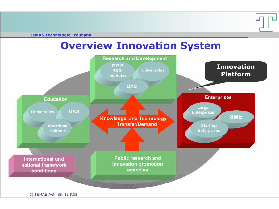
TEMAS Technologie Treuhand
International und national framework
conditions
Education
Research and Development
UniversitiesP-P-P R&D-
Institutes
UAS
LargeEnterprises
SMEStart-up
Enterprises
UASUniversities
Vocationalschools
Education
Source: according to Hotz, Good, Küchler, Reuter
Enterprises
Knowledge Transfer/Demand
Public research andInnovation promotion
agencies
Overview Innovation System
and Technology
Innovation Platform
© TEMAS AG: 67 31.5.05
TEMAS Technologie Treuhand
Outlook
4 Safety and risk issues
4 Technology
4 Collaboration Science and Economy– Knowledge and Technology Transfer– Education
© TEMAS AG: 68 31.5.05
TEMAS Technologie Treuhand
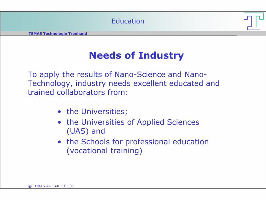
Needs of Industry
To apply the results of Nano-Science and Nano-Technology, industry needs excellent educated and trained collaborators from:
• the Universities;• the Universities of Applied Sciences
(UAS) and• the Schools for professional education
(vocational training)
Education

© TEMAS AG: 69 31.5.05
TEMAS Technologie Treuhand
The cornerstones for a successful Knowledge and Technology Transfer from academic research into industry:
a) University level:- Actively support PhD students and motivated university
graduates to embark upon a PhD study. (www.nano-world.org)- International summer school “Hansliberg/Twannberg” - PhD student award (www.ethrat.ch/topnano21)
b) Universities of Applied Sciences:- Encouragement and assistance to develop national teaching courses in Nano Technologies. - Support to create the UAS Nano Platform (www.nanofh.ch)
c) Vocational schoolsVocation specific teaching modules addressing the application of tools for the Nano scale (AFM, STM, …) for surface inspection such as roughness, contaminations, … . (www.nanoforschools.ch)
Education

© TEMAS AG: 70 31.5.05
TEMAS Technologie Treuhand
CTI Start-up professional coaching process
Pre- label coaching Post-label support
Source: CTI Start-up

© TEMAS AG: 71 31.5.05
TEMAS Technologie Treuhand
Innovation means seeing
what everybody sees and anticipating
what no one has anticipated
www.temas.ch(Download presentation)
(News letter)
TEMAS Ltd.The Innovation Company