idealprogram dsa activity at leti - 株式会社screen ... ideal (dsa) project... · bf bd sz0 bf...
TRANSCRIPT

IDeAL program : DSA activity at LETI
S. Tedesco ‐ R. Tiron ‐ L. Pain
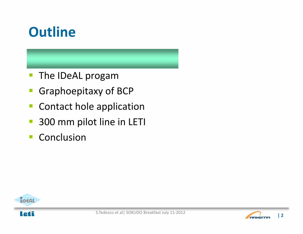
Outline
Why DSA for microelectronicsTh ID AL The IDeAL progam
Graphoepitaxy of BCP Contact hole application 300 mm pilot line in LETI Conclusion
© CEA. All rights reserved| 2S.Tedesco et al| SOKUDO Breakfast July 11‐2012

Why DSA for Microelectronics ?
Block copolymers self assembly capabilities Very high resolution Low intrinsic Line Edge Roughness Easy process Low cost
C‐MOS Lithography constraints Control the domain orientations (1D ‐ 2D) Alignment control with respect to a preview level Integration capabilities Low defectivity Respect of design r les Respect of design rules
© CEA. All rights reserved| 3S.Tedesco et al| SOKUDO Breakfast July 11‐2012

Why DSA for Microelectronics ?
60
universities
industry and large labs
Advanced lithography SPIE conferences
40
50
DSA
20
30
of p
aper
s on
D
0
10
20
nb
02010 2011 2012
DSA a complementary lithography techniques that could get
© CEA. All rights reserved| 4S.Tedesco et al| SOKUDO Breakfast July 11‐2012
DSA a complementary lithography techniques that could get inserted as early as the 14nm node

Outline
Why DSA for microelectronicsTh ID AL The IDeAL progam
Graphoepitaxy of BCP Contact hole application 300 mm pilot line in LETI Conclusion
© CEA. All rights reserved| 5S.Tedesco et al| SOKUDO Breakfast July 11‐2012

LETI DSA open program
Insertion of Directed self Assembly LithographyInsertion of Directed self Assembly Lithography
© CEA. All rights reserved| 6S.Tedesco et al| SOKUDO Breakfast July 11‐2012

Directed Self Assembly : the lithography?
Objectives A new open program to develop a full DSA solution Joint work in LETI environment on material processes demonstration & Joint work in LETI environment on material, processes, demonstration &
integration A cluster open to materials and equipments’ suppliers, IDM, EDA
Partnership status July 2012 Partnership status – July 2012 DSA material development
Copolymer material worldwide leader : Collaboration with academic laboratories resist partners : under progress
Equipment suppliers2 i d t i l t 2 industrial partners
End users Bilateral work with
© CEA. All rights reserved| 7S.Tedesco et al| SOKUDO Breakfast July 11‐2012

Arkema in a few points
Worldwide player in specialties chemistry Ranging from 1st to 3rd position in product lines insuring 80% Ranging from 1st to 3rd position in product lines insuring 80%
of the company revenue. 2010 revenue : 5,9 Md€ R&D : > 120M€ / 8 R&D center WW (US, Japan, France) Annual Capex : 293 M€ 80 industrial sites 15 000 employees
ARKEMA strength : Worldwide polymer manufacturer Strong know‐how on block copolymer Ability to quickly ramp‐up from R&D to industrial scale
© CEA. All rights reserved| 8S.Tedesco et al| SOKUDO Breakfast July 11‐2012

missions ?
Push material platforms to maturity From lab scale to industry From lab scale to industry Evaluate advanced copolymer platform
Develop 300mm patterning solutions Certify material compatibility with clean room standard Screen DSA material performances Screen DSA material performances Verify transfer capabilities
Scale‐up DSA processes to production level Compatibility with design rules Respect of ITRS standard defectivity throughput
© CEA. All rights reserved| 9S.Tedesco et al| SOKUDO Breakfast July 11‐2012
Respect of ITRS standard : defectivity, throughput…

How to go from R&D to industrial ?A production‐oriented consortium
DSA MaterialsDSA Materials IntegrationIntegrationDSA MaterialsDSA Materials IntegrationIntegration
Industrial scalability
300 mm INTEGRATION – Defectivity– Design compatibility
Mat
urity
III
catio
n
Industrial scalability
300 mm INTEGRATION – Defectivity– Design compatibility
Mat
urity
III
catio
n
Process developmentProcess development
Pre-industrial First 300 mm demonstration ty II
rial q
ualif
ic
rializ
atio
n
Process developmentProcess development
Pre-industrial First 300 mm demonstration ty II
rial q
ualif
ic
rializ
atio
n
reactor – Process development– Etch, Strip, …
Mat
urit
e-up
mat
er
Indu
strreactor – Process development
– Etch, Strip, …
Mat
urit
e-up
mat
er
Indu
str
Lab. scaleSamples:– Material compatibility– Material properties
Mat
urity
I
Process capability– Throughput– Patterning capability
Scal
e
Lab. scaleSamples:– Material compatibility– Material properties
Mat
urity
I
Process capability– Throughput– Patterning capability
Scal
e
© CEA. All rights reserved| 10S.Tedesco et al| SOKUDO Breakfast July 11‐2012

ARKEMA – LETI partnership : materials path
Efficient neutralization layer Several materials under screening
PS‐PMMA platform High platform
CD = 7nm CD = 7nmCD = 7nmCD = 7nm CD = 7nmCD = 7nmCD 15nm CD 15nm
100 nm 200 nm100 nm100 nm100 nm 200 nm200 nm200 nm
High BCPPS-b-PMMA BCP
200 nm 200 nm
© CEA. All rights reserved| 11S.Tedesco et al| SOKUDO Breakfast July 11‐2012

Outline
Why DSA for microelectronicsTh ID AL The IDeAL progam
Graphoepitaxy of BCP Contact hole application 300 mm pilot line in LETI Conclusion
© CEA. All rights reserved| 12S.Tedesco et al| SOKUDO Breakfast July 11‐2012

Why grapho‐epitaxy preference ?A versatile process
HSQ e-Beam resist 193nm PCAR
LETI demonstration Graphoepitaxy
193nm PCAR
Leti approach
193nm PCAR 193nm NTD Contact shrink
© CEA. All rights reserved| 13S.Tedesco et al| SOKUDO Breakfast July 11‐2012

How to find optimum guiding litho process ?
A=> Influence of Litho1 design => Influence of Litho1 design rules & BCP material rules & BCP material
200 nmB
C a0
© CEA. All rights reserved| 14S.Tedesco et al| SOKUDO Breakfast July 11‐2012
200 nmDesign rule compatibility “Optimization of block copolymer self-assembly through graphoepitaxy: A defectivitystudy” R.Tiron et al., JVST B29 06F206 (2011)

Zero Defect Configuration
Before litho1Before litho1Before litho1 Before litho1 optimization optimization
500 nm
After litho1 After litho1 optimization optimization
500 nm
pp
© CEA. All rights reserved| 15S.Tedesco et al| SOKUDO Breakfast July 11‐2012
Defectivity measurement enables lithography and process optimization

Silicon Etching with Copolymer LithographyInitial mask (PS)Initial mask (PS)
30 to 100 nm thick
SiO2 Mask(10 nm)
Si Mask etching(CF4 based plasma)
Silicon etching(HBr/Cl2/O2 plasma)
Si
Brush opening(Ar/O2 plasma)
PS plasma treatment
Si Si
PS plasma treatment
etching on graphoepitaxy
Copolymer etching process fully compatible with CMOS requirements
© CEA. All rights reserved| 16S.Tedesco et al| SOKUDO Breakfast July 11‐2012
“Self-assembly patterning using block copolymer for advanced CMOS technology: optimisation of plasma etching process”Thierry Chevolleau, CNRS (France)- Paper 8328-20, SPIE2012

Silicon Etching with Copolymer Lithography
f f C S T f f BCP i t 193Transfer of BCP into Si by using SiO2 hard mask
Transfer of BCP into 193 nm trilayer
50 nm50 nm50 nm50 nm
© CEA. All rights reserved| 17S.Tedesco et al| SOKUDO Breakfast July 11‐2012
Copolymer etching process fully compatible with CMOS requirements

Outline
Why DSA for microelectronicsTh ID AL The IDeAL progam
Graphoepitaxy of BCP Contact hole application 300 mm pilot line in LETI Conclusion
© CEA. All rights reserved| 18S.Tedesco et al| SOKUDO Breakfast July 11‐2012

Contact shrink and multiplication using DSA of BCP Aft BCP t hiAft BCP t hiAfter 193nm litho.After 193nm litho. After BCP DSAAfter BCP DSA After BCP etchingAfter BCP etching
Contact Contact Shrink Shrink 100 nm100 nm
Contact Contact MultiplicationMultiplication
100 nm100 nm
© CEA. All rights reserved| 19S.Tedesco et al| SOKUDO Breakfast July 11‐2012
Integration (litho+etch) demonstrated for contact shrink and multiplication

How to define design rules: Example of code
Design
BF BD SZ0 BF BD+2% SZ+0.5 BF BD-2% SZ-0.5
Calculated CH placement
Simulation contourContour variation w.r.t. dose, focus and mask CD error variations
53+ Extracted Contour
Experimental validationExperimental validation
53nm+ Calculated CH
position
CH position on
© CEA. All rights reserved| 20S.Tedesco et al| SOKUDO Breakfast July 11‐2012
wafer

Outline
Why DSA for microelectronicsTh ID AL The IDeAL progam
Graphoepitaxy of BCP Contact hole application 300 mm pilot line in LETI Conclusion
© CEA. All rights reserved| 21S.Tedesco et al| SOKUDO Breakfast July 11‐2012
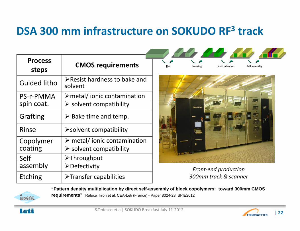
DSA 300 mm infrastructure on SOKUDO RF3 track
Process steps CMOS requirements h Self assemblyfreezing neutralizationh Self assemblyfreezing neutralization
steps
Guided litho Resist hardness to bake and solvent
PS‐r‐PMMA metal/ ionic contaminationspin coat. solvent compatibility
Grafting Bake time and temp.
Rinse solvent compatibilityRinse solvent compatibility
Copolymer coating
metal/ ionic contamination solvent compatibility
Self Throughput
Front‐end production 300mm track & scanner
Self assembly
Throughput Defectivity
Etching Transfer capabilities
“Pattern density multiplication by direct self assembly of block copolymers: toward 300mm CMOS
© CEA. All rights reserved| 22S.Tedesco et al| SOKUDO Breakfast July 11‐2012
“Pattern density multiplication by direct self-assembly of block copolymers: toward 300mm CMOS requirements” Raluca Tiron et al, CEA-Leti (France) - Paper 8324-23, SPIE2012

Shrink of contact holes 300mm process
graphoepitaxy with standard lithography 193nm
Si
SOC
SOCSiARC
BCPSiARC
Si
CD ~ 100nm CD ~ 15nm
0.2µm 0.2µm
© CEA. All rights reserved| 23S.Tedesco et al| SOKUDO Breakfast July 11‐2012

Shrink of contact holes 300mm processnorth
t tt center eastwest
south
0.5µm
© CEA. All rights reserved| 24S.Tedesco et al| SOKUDO Breakfast July 11‐2012

Outline
Why DSA for microelectronicsTh ID AL The IDeAL progam
Graphoepitaxy of BCP Contact hole application 300 mm pilot line in LETI Conclusion
© CEA. All rights reserved| 25S.Tedesco et al| SOKUDO Breakfast July 11‐2012

To conclude
DSA a complementary lithography technique thatcould get inserted as early as the 14nm nodecou d get se ted as ea y as t e ode– In a firs step by using PS‐b‐PMMA like materials– In a second step by using high materials
A realistic application: contact hole shrink anddoublingdoubling
Defectivity is keyDefectivity is key
Thanks for SOKUDO involvement and support
© CEA. All rights reserved| 26S.Tedesco et al| SOKUDO Breakfast July 11‐2012
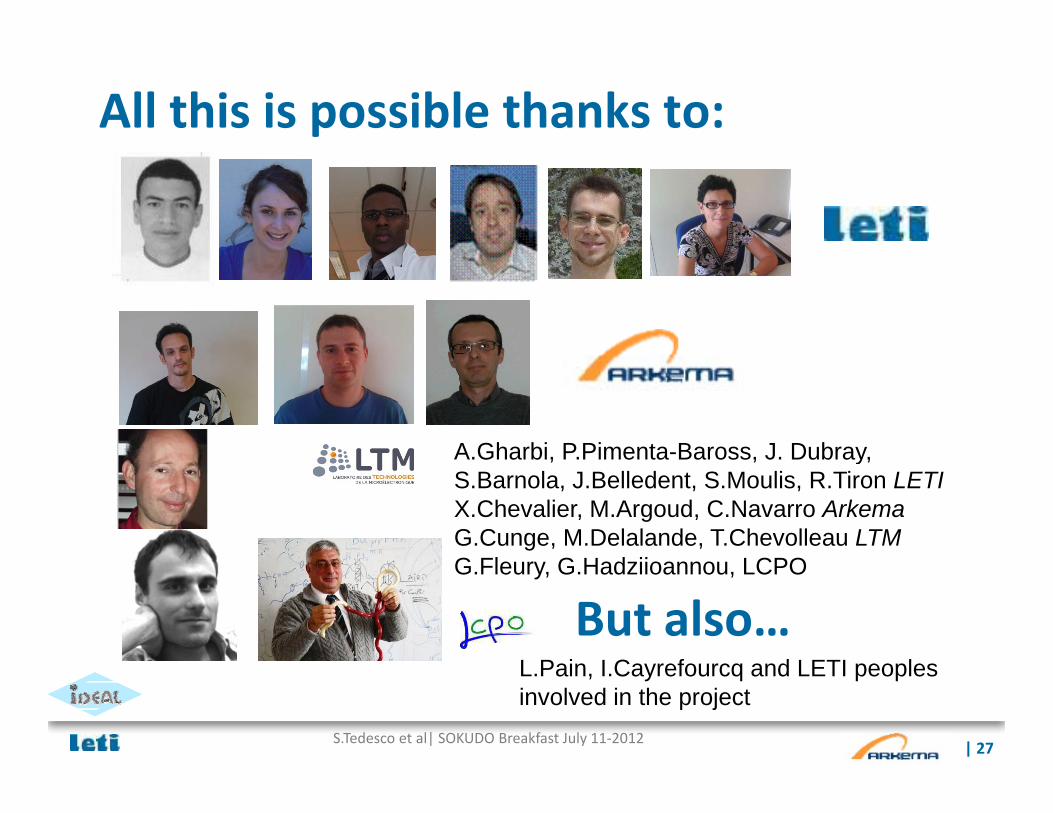
All this is possible thanks to:
A.Gharbi, P.Pimenta-Baross, J. Dubray,A.Gharbi, P.Pimenta Baross, J. Dubray, S.Barnola, J.Belledent, S.Moulis, R.Tiron LETIX.Chevalier, M.Argoud, C.Navarro ArkemaG.Cunge, M.Delalande, T.Chevolleau LTMG Fl G H d ii LCPOG.Fleury, G.Hadziioannou, LCPO
But also…L P i I C f d LETI l
© CEA. All rights reserved| 27S.Tedesco et al| SOKUDO Breakfast July 11‐2012
L.Pain, I.Cayrefourcq and LETI peoples involved in the project