hydrogen-plasma-enhanced crystallization of · pdf filehydrogen-plasma-enhanced...
TRANSCRIPT

Hydrogen-Plasma-Enhanced
Crystallization of Hydrogenated
Amorphous Silicon Films: Fundamental
Mechanisms and Applications
,
Kiran Pan gal
A DISSERTATION
PRESENTED TO THE FACULTY
OF PRINCETON UNIVERSITY
IN CANDillACY FOR THE DEGREE
. OF DOCTOR OF PHILOSOPHY
RECOMMENDED FOR ACCEPTANCE
BY THE DEPARTMENT OF
ELECTRICAL ENGINEERING
NOVEMBER 1999
Supported by DARPA/ONR N66001-97-1-8904 and Program in PlasmaScience and Technology, DOE DE-ACO2-76-CHO-3073

@ Copyright 1999 by Kiran Pangal.
All rights reserved.
;
I
t.
11
i i
",.,
" ",", ~"
I
Dedicated to my parents and sister
.,'. ~
iii
_~iC ~ ~'c

ABSTRACT
The crystallization of hydrogenated amorphous silicon (a-Si:H) deposited by
plasma-enhanced chemical vapor deposition (PECYD) by thermal annealing is of great
interest for display and silicon-on-insulator (SOl) technologies. For large area
electronics, there has been considerable interest to integrate both a-Si:H TFTs, for low
leakage in the OFF state, and poly-Si TFTs, for high drive currents, on the same
substrate, for example, to integrate polysilicon drivers in flat panel displays using a-
Si:H TFTs in pixels. There is interest also to achieve high mobility polysilicon TFTs
fabricated at low temperatures (~ 600°C). Low thermal budgets are necessary so that
glass substrates can be used in case of display applications, and damage to preexisting
devices is minimized in case of 3-D integrated circuit applications. In this thesis we will
describe the use of selective crystallization using hydrogen plasma seeding treatment of
a-Si:H layers to achieve both these aims.
We have found that a room temperature hydrogen plasma exposure in a parallel-
plate-diode-type Reactive Ion Etcher (RIB) can reduce crystallization time of a-Si:H by
a factor of five. Exposure to hydrogen plasma reduces the incubation time, while the
rate of crystallization itself is not greatly affected. This plasma-enhanced crystallization
can be spatially controlled by masking with patterned oxide, so that both amorphous
and polycrystalline areas can be realized simultaneously at desired locations on a single
substrate. The enhancement of crystallization rate is probably due to the creation of seed
nuclei at the surface and the effect is limited to the top 30-40 nm of the a-Si:H layer.
We have used these films to fabricate low-temperature (~600°C) self-aligned n-
channel polycrystalline transistors. Well-behaved characteristics were obtained in all 'j
IV
i~y~ I

""--
cases. All the samples had mobilities in the range of 35-40 cm2Ns despite the short
crystallization time in the hydrogen-plasma treated sample.
Lateral-seeded growth from seeded regions in the source and drain regions
resulted in higher performance TFfs with the field-effect mobility increasing for
channel lengths shorter than 5 ~m. The seeding was done by exposure to hydrogen
plasma after the active region and the gate was patterned. The seeded-low-temperature
TFfs had a field-effect mobility of -75 cm2Ns for channel length of -2 ~m, nearly
twice that of unseeded TFfs.
We have also demonstrated a method for integrating a-Si and poly-Si transistors
together starting with a single Si layer with no laser processing involved, combining
many of the fabrication steps between the two transistors, so that making both a-Si:H
and poly-Si TFfs of high performance is not much more work than making just one
type of transistor.
,Ii
V

ACKNOWLEDGEMENTS
Acknowledging others for their help and understanding is usually the most
difficult albeit important part of a thesis and is therefore usually done at the end. I
would like to begin by thanking my advisor Prof. James C. Sturm for his help, guidance
and support without which this endeavor would not have been possible. Special thanks
are also due to Prof. Sigurd Wagner for allowing me to use the equipment in his
laboratory, for all the helpful discussions, and lastly but not the least, for taking time to
read this thesis. I would also like to thank Prof. Steven Chou for reading this thesis.
Words cannot describe the appreciation I feel for all the strength and support I
derived from my loving parents and sister. It has been a long journey, with its share of
successes and disappointments and their support has been invaluable.
I would like to thank all members of the Sturm group for their help and all the
discussions we had about the laboratory, the research work, and any other topic under
the sun. It made the whole graduate student experience thoroughly enjoyable.
A special thank you goes to all the students and research staff in Prof. Wagner's
group for teaching me to use the various pieces of equipment in their laboratory and for
helping me comprehend the physics of amorphous silicon.
The faculty and staff of the EMD group here at Princeton are instrumental in
creating the right atmosphere for research. I would like to thank Dr. Nan Yao at the
Princeton Materials Institute for his help with transmission electron microscopy
experiments. Many thanks are due to Dr. Steven Theiss at Lawrence Livermore
National Laboratory for growing the low-temperature magnetron-PECVD oxide, and to
Prof. P. M. Fauchet and his research staff at University of Rochester for Raman
,,.
VI
~

measurements of the samples. I would also like to thank Mike Valenti, Joe Palmer and
Dr. Duane Marcy for all their help, and for keeping the clean-room running smoothly.
Finally, no acknowledgment would be complete without thanking all my friends,
and my aunt, uncle and my two cousins, who made my stay at Princeton a very
pleasurable and hassle-free experience.
,
:
VII
.,'" Ii ~,

OUTLINE
Abstract iv
Acknowledgements vi
I. Introduction 1
1.1 Motivation 1
1.2 Thesis outline 4
II. Crystallization of Amorphous Silicon 6
2.1 Introduction 6
2.2 Solid phase crystallization 8
2.2.1 Introduction 8
2.2.2 Annealing techniques 11
2.2.3 Nucleation enhancement techniques 13
2.3 Laser crystallization 18
2.4 Zone-melt recrystallization 22
2.5 Summary 23
References 24
III. Enhancement of Crystallization of Hydrogenated Amorphous
Silicon by a Hydrogen Plasma Treatment 29
3.1 Introduction 29
3.2 Experimental procedure 30
3.2.1 Substrate preparation, a-Si:H film growth, and
characterization methods 30l
3.2.2 Plasma treatment and anneal 34
3.2.3 Other sample preparation and analysis techniques 37 ;.
viii
_or"'"
3.3 Crystallization of plasma-treated films 39
3.3.1 Introduction 39
3.3.2 Effect of annealing temperature 40
3.3.3 Effect of RF power and plasma exposure time 43
3.3.4 Effect of deposition temperature 43
3.3.5 Effect of film thickness 47
3.3.6 Effect of dopant in the film 48
3.3.7 Selective crystallization 49
3.3.8 Material characteristics of the films 52
3.4 Mechanism of seeding by hydrogen plasma 55
3.4.1 Location of seed nuclei 56
3.4.2 Possible structure of seed nuclei 58
3.4.3 Discussion 64
3.5 Oxygen-plasma-enhanced crystallization 69
3.6 Summary 71
References 72
IV. Polycrystalline Silicon Thin-Film Transistors 76
4.1 Introduction 76
4.2 Precursor silicon film deposition and crystallization 79
4.3 High-temperature transistors 80
4.3.1 Fabrication details 80
4.3.2 Results and discussion 85
4.4 Low-temperature transistors 90
4.4.1 Fabrication details 90
4.4.2 Results and discussion 92
IX
,"""",~:C!

4.5 Laterally-seeded transistors 103
4.5.1 Device concept 103
4.5.2 Selective crystallization 105
4.5.3 Fabrication of laterally-seeded transistors 106
4.5.4 Results and discussion 109
4.6 Summary 120
References 121
V. Integrated Amorphous and Polycrystalline Silicon Transistors 123
5.1 Introduction 123
5.2 Experimental procedure and measurement techniques 125
5.2.1 Sample growth and crystallization 125
5.2.2 Measurement techniques 126
5.3 Hydrogen effusion during anneal and rehydrogenation 128
5.4 Transistor performance optimization 134
5.4.1 Fabrication details 134
5.4.2 Techniques to minimize channel-etch damage 138
5.4.3 Results and discussion 142
5.5 Summary 159
References 160
VI. Solid Phase Crystallization: Techniques to Realize
Silicon-on-Insulator 162
6.1 Introduction 162
6.2 Techniques to realize large grains 164
6.2.1 Annealing temperature and effect of disorder in a-Si films 165
6.2.2 Multiple-stepanneal 167
x
.

6.2.3 Suppress nucleation at the a-Si/substrate interface 168
6.2.4 Secondary grain growth 169
6.3 Techniques to control grain boundary locations 171
6.3.1 Lateral solid phase epitaxy 171
6.3.2 Selective-nucleation-based epitaxy 173
6.3.3 Other selective seeding/lateral crystallization techniques 174
6.4 Techniques to minimize and passivate defects 178
6.4.1 Techniques to minimize crystalline defects 178
6.4.2 Passivation of defects 181
6.5 Grain orientation 182
6.5.1 Graphoepitaxy 185
6.6 Summary and future work 187
References 192
VII. Micro-Electro-Mechanical Charge-Sensing Devices for Plasma-Process-
Induced Charging Damage Measurement 196
7.1 Introduction 196
7.2 Plasma-induced charging: An overview 198
7.2.1 Causes of plasma-induced charging 199
7.2.2 Techniques to evaluate charging in plasmas 202
7.2.3 Techniques to minimize plasma-induced charging
damage 205
7.3 MEMS charge-sensing device 207
7.3.1 Concept 207
7.3.2 Modeling 208
7.3.3 Fabrication details 214
Xl
.,,1
7.3.4 Results and discussion 219
7.4 Correlation of sensor results with device degradation 229
7.4.1 Fabrication details 230
7.4.2 Plasma damage measurement 232
7.4.3 Effect of UV damage 239
7.5 Summary and future work 243
References 244
VIII. Conclusion 247
8.1 Summary (, 247
8.2 Future work 249
References 250
Appendix A. Growth Recipes 251
A.1 Undoped a-Si:H 251
A.2 Doped a-/~c-Si:H 252
A.3 a-SiNx:H 253
A.4 Hydrogenation 253
Appendix B. Amorphous Silicon Characterization Techniques 255
B.1lnfrared transmission 255
B.2 Optical transmission and photothermal deflection spectroscopy 256
B.3 Dark conductivity 261
References 263
Appendix C. Publications and Presentations Resulting from this Thesis 264
C.1 Publications 264
C.2 Conference presentations 265
~
XII
~~"'C~C' I '~
.tt~1

.. -
LIST OF TABLES
4.1. Process conditions, and self-aligned polysilicon low-temperature n-channel «600
°C) TFf results, showing the effect of the blanket-plasma-seeding treatment 93
4.2. Laterally-seeded polysilicon TFfs characteristics for various growth and process
conditions 108
5.1. Non-self-aligned n-channel integrated polysilicon and a-Si:H TFf characteristics
for different processing conditions 143
7.1. Comparison of plasma-induced damage measurement techniques 203
7.2. Charging voltage for oxygen plasma (60 W, 150 mtorr, 15 sccm) as measured by
MEMS charge sensor at various locations on 100-mmSi wafer in different
configurations 228
I
xiii I
1~I~ I

LIST OF FIGURES
2.1 Schematic illustration of the various phase transformations occurring upon pulsed-
laser irradiation of an a-Si film 20
3.1 Schematic layout of the S900 multi-chamber PECVD system 32
3.2 UV reflectance spectrum of single-crystal and amorphous silicon, and band diagram
of single-crystal silicon 36
3.3 Change in UV reflectance at 276 nm as a function of annealing time for untreated
and plasma-treated a-Si:H samples 40
3.4 Total crystallization time of untreated and hydrogen-plasma-treated samples as a
function of annealing temperature 41
3.5 Crystallization time of plasma-treated samples as function of RF power and time
during the plasma treatment 42
3.6 Hydrogen content and crystallization time of a-Si:H films as function of deposition
temperature 44
3.7 Infrared absorption coefficient of a-Si:H films deposited on bare Si wafers at
various temperatures 45
3.8 Crystallization time of untreated and hydrogen-plasma-treated samples as a function
of the a-Si:H film thickness 47
3.9 Sheet resistance and crystallization time of phosphorus-doped films 49
3.10 Optical micrograph showing selective and lateral crystallization 50
3.11 X-ray diffraction of polysilicon untreated and plasma-treated films 53
3.12 Plan-view transmission-electron microscopy of blanket and laterally-hydrogen-
plasma-seeded films 54
,i
XIV
- ""C~, l

3.13 Crystallization time and absorption at 2100 cm-l of samples etched to different
depths 57
3.14 Thickness of the hydrogen-plasma-modified layer as a function of exposure time to
the hydrogen plasma 58
3.15 The infrared spectra of untreated and plasma-treated films 59
3.16 Integrated absorption at 2000 and 2100 cm-l as a function of hydrogen seeding
plasma exposure time 60
3.17 Hydrogen and oxygen concentration in a-Si:H films before and after hydrogen
plasma treatment 61
3.18 Aluminum concentration in the a-Si:H films 63
3.19 Raman shift of untreated and hydrogen-plasma-treated a-Si:H films 67
3.20 Schematic illustration of reaction occurring at a-Si:H film surface during
hydrogen-plasma-seeding treatment 69
3.21 Hydrogen and oxygen concentration in a-Si:H films before and after oxygen
plasma treatment 70
4.1 Simplified self-aligned TFr cross-section 81
4.2 Effect of hydrogenation on high-temperature TFf characteristics 87
4.3 Linear and subthreshold characteristics of high-temperature TFrs in untreated and
hydrogen-plasma-blanket-seeded films 89
4.4 Field-effect mobility as function of effective channel length of high and low-
temperature TFrs 90
4.5 Linear and subthreshold characteristics of low-temperature TFTs in untreated and
hydrogen-plasma-blanket-seeded films 94
4.6 Field-effect mobility as function of effective channel length of low-temperature
TFrs in untreated and hydrogen-plasma-blanket-seeded films 95
xv
"""~,I!
4.7 Threshold voltage as function of effective channel length of low-temperature TFfs
in untreated and hydrogen-plasma-blanket-seeded films 98
4.8 Field-effect mobility as function of effective channel length of low-temperature
TFfs in hydrogen-plasma-blanket-seeded films for different growth temperatures 100
4.9 Schematic illustration of laterally hydrogen-plasma-seeded TFf fabrication
sequence 104
4.10 Subthreshold and linear characteristics of laterally-hydrogen-plasma-seeded and
blanket-un seeded polysilicon TFfs 110
4.11 Field-effect mobility and threshold voltage for different effective channel lengths
for laterally-hydrogen-plasma-seeded and blanket-un seeded polysilicon TFfs annealed
at 600 DC 112
4.12 Plot of 1/IDs as function of drawn channel length for different values of [VGS-VTH]
I to extract the effective channel length 113
4.13 Field-effect mobility for different effective channel lengths for laterally-hydrogen
plasma-seeded and blanket-unseeded polysilicon TFfs annealed at 625 DC 115
4.14 Subthreshold characteristics of laterally-seeded TFfs with lateral crystallization
done before and after source/drain ion implantation step 116
4.15 Subthreshold characteristics of laterally-seeded TFfs from crystallization at 600
DC of a-Si:H films deposited at 150 and 250 DC 117
4.16 Effect of N 20 plasma treatment on the PECVD gate oxide 119
5.1 Infrared absorption coefficient at 630 cm-l for as-deposited, after-anneal, and
rehydrogenated a-Si:Hfilms 129
5.2 Infrared absorption coefficient at 2000 cm-l for as-deposited, after-anneal, and
rehydrogenated a-Si:H films 130
xvi
i "1 ',
5.3 Photothermal deflection spectra of optical absorption coefficient of a-Si:H films in
the as-deposited, annealed, and rehydrogenated states 131
5.4 Tauc's plot of (cx.nE) 1/2 vs. photon energy of as-grown, annealed and rehydrogenated
films 132
5.5 Dark conductivity measurement of the a-Si:H samples 133
5.6 Integrated a-Si:H and polysilicon top-gate non-self-aligned transistor fabrication
steps 135
5.7 Exaggerated cross-section of a-Si:H/poly-Si TFT showing the effect of non-
coplanar contacts and overetch during channel-definition step on source/drain
resistance 136
5.8 Schematic cross-section of sample during channel-definition step with n+ ~c-Si:H
deposited after active islands were patterned 139
5.9 Fabrication sequence ofTFTs with inverted source/drain contacts, i.e., the n+ ~c-
Si:H is deposited first followed by intrinsic layer 141
5.10 Subthreshold characteristics ofa-Si:H TFTs for precursor a-Si:H growth
temperatures of 150 and 250 °c 145
5.11 Best a-Si:H TFT characteristics for growth temperature of 150 °c, selective
crystallization anneal at 625 °c 149
5.12 Field-effect mobility of the a-Si:H transistors for different rehydrogenation
conditions 152
5.13 Net hydrogen content in a-Si:H films after rehydrogenation for various exposure
times 153
5.14 Subthreshold characteristics of a-Si:H TFT before and after post metal
hydrogenation 156
, iI
,XVII
I
~""'"-i!- i
~i"';c

5.15 Subthreshold characteristics of optimized integrated a-Si:H and poly-Si TFfs
made in same a-Si:H precursor film 158
6.1 Schematic illustration of the mode of crystal growth considering heterogeneous
nucleation at the interface 183
6.2 Schematic fabrication sequence to realize defect-free single-crystal silicon islands
using hydrogen-plasma seeding 189
7.1 Schematic model showing wafer charging of oxide exposed to uniform and
nonuniform plasma 200
7.2 Schematic diagram showing the cause of charging-current stress due to nonuniform
plasmas 201
7.3 Schematic diagram showing the cause of charging-current stress due to electron
shading effect 202
7.4 Schematic cross-sections of CHARM-2 charge sensor 204'.
7.5 CHARM-2 charge sensors with different value of charge-sensing resistors allowing
the reconstruction of the current-voltage characteristics of the charging source 205
7.6 Microscopic charge-sensing structure for uncharged and charged surfaces 208
7.7 Top and side views of the paddle and torsional mirror 209
7.8 Tip deflection vs. voltage for paddle structure and simple cantilever of same length
(simulated) 210
7.9 Simulation results of paddle structure 212
7.10 Simulation results of torsional mirror 213
7.11 Fabrication sequence of the paddle structure 216
7.12 Scanning electron micrographs of the finished paddle structure 218
7.13 Set-up used for calibrating the MEMS charge sensors externally 220
7.14 Set-up used to detect plasma induced charging directly 221
XVIII
-
7.15 Comparison of ex -situ and in-situ methods to detect charging 223
7.16 Charging voltage as function of RF power and chamber pressure during exposure
to oxygen plasma 224
7.17 Charging voltage as function of position across the electrode and flow rate of gas
during exposure to oxygen plasma 225
7.18 100-mm Si wafer showing the positions of charge sensors 226
7.19 Cross-sections of different configurations used to bond sensors on to the 100 mm
Si wafer 227
7.20 J - V characteristics of charging source and charging damage seen by MOS devices
with different oxide thickness 230
7.21 Cross-section of the capacitor used to study charging damage 231
7.22 Quasi-static C- V curves and corresponding interface-state-trap density for
exposure to Ar plasma at varying powers 235
7.23 Flat-band voltage and interface-state density change after plasma exposure 236
7.24 Comparison of QS C- V curves of MOS capacitors after plasma exposure and DC
bias stressed externally 237
7.25 Charging voltage during exposure to Ar plasma inferred from externally DC bias
stressing and QS C- V matching 238
7.26 Comparison of charging voltage as measured by MEMS charge sensor and inferred
from QS C- V matching 239
7.27 High frequency C- V curves and flat-band voltage shift of MNOS capacitors after
plasma exposure 240
7.28 QS C- V curves of MOS capacitors with different aluminum gate thickness
showing the effect of UV damage 242
"
~
XIX
I
Chapter 1
""';j~
INTRODUCTION
1.1 MOTIVATION
The last decade has seen tremendous interest in thin silicon films on insulating
substrates, from fundamental studies on growth and material properties of the films to
actual devices, be they thin-film transistors, sensors, or other device applications.
Especially, thin-film transistors (TFfs) have received increasing attention for their use
in active matrix liquid crystal displays on glass (or fused quartz) substrates for use as
pixel-switching transistors or in the row/column circuits, and in silicon-on-insulator
(SOl) technologies for three-dimensional integration of devices on silicon substrates.
Three-dimensional (3-D) integration is useful for both packing density and system
architecture. Furthermore, thin (i. e. <100 nm) SOl layers are attractive for devices with
very small dimensions from both a technological and fundamental point of view.
Technologically, the thin SOl films make it easy to isolate devices and to avoid
parasitic short channel effects such as subsurface drain-induced barrier lowering.
Fundamentally, the thin films make it easy to have the channel gated from multiple
sides so that tight confinement of the carriers in the narrow channel can be achieved.
Historically, the realization of SOl layers has been difficult as direct deposition
of silicon on insulating films yields either amorphous or polycrystalline silicon
(polysilicon) films, depending on the growth conditions. Amorphous silicon films have
iI,J!
Chapter 1: Introduction 2
very poor carrier mobility and are therefore unsuitable for most applications. However,
properties of polysi1icon films are closer to that of crystalline Si. Various techniques
have been developed to improve the quality of the polysilicon films so that single-
crystal like behavior is realized. The two leading approaches towards SOl are the
SIMOX technique, in which a buried oxide layers is formed in a single crystal substrate
through high energy oxygen implantation and annealing at 1200 °c or higher, and the
bond-and-etch-back technique, in which a single crystal is bonded to an oxide layer
(usually at 900 °c or higher), and then chemically and mechanically polished back to a
thin layer. Neither of these techniques is suitable for fabrication of multiple thin layers
of devices due to the high temperatures involved and the difficulty in controlling the
thickness of the silicon films. These methods are especially not applicable in displays
where silicon films on transparent substrates are required.
The most widespread and prevalent technique to realize silicon films on
insulating substrates, for large area applications, is crystallization of precursor
amorphous silicon film to realize polysilicon films. We will discuss the various methods
that have been studied to crystallize silicon films in detail later in chapter 2. There is a
need to obtain large grain polycrystalline silicon films or nearly single-crystal silicon,
with smooth surfaces. For 3-D integration purposes, there is also a need:to control the
locations of grain boundaries so that device can be fabricated within a single grain
thereby achieving single-crystal like behavior. In addition to these constraints on the
material characteristics of the polysilicon films, a low thermal-budget process is
essential, especially for AMLCDs fabricated on glass substrates (to avoid degradation
of glass substrate due to thermal damage), and for three-dimensional IC technology (to
avoid thermal damage to the pre-existing devices).
~7CI I
_~ii

Chapter 1: Introduction 3
In addition to these requirements, for display applications there is need for
developing a process/technique to integrate amorphous silicon transistors, which are
used as pixel-switching transistors due to low leakage in the OFF state, and
polycrystalline silicon transistors, which are used in the row/column driver circuits, on
the same substrate to reduce costs. This requires that the crystallization process be a low
temperature process and be selective so that amorphous and polycrystalline regions can
be realized simultaneously on the same substrate. iIn our work, we found that a hydrogen plasma treatment of thin hydrogenated
amorphous silicon (a-Si:H) films deposited by plasma-enhanced chemical vapor I
deposition results in reduction of subsequent crystallization time of the films, and that
this effect can be controlled so that only certain regions of the films are seeded. We
studied this plasma-enhancement effect further to understand the mechanism and its
effect on the properties of the polysilicon films. We then fabricated n-channel
transistors in these plasma-treated films with reduced crystallization time of -4 h at a
process temperature of only 600 °c. We also used this technique to control grain
boundaries locations and thereby fabricate transistors with higher mobility. This was
accomplished by selective seeding the source and drain regions of the transistor
followed by crystallization anneal so that lateral crystallization into the channel regions
occurs.
By masking the a-Si:H films during the plasma treatment, polycrystalline and
amorphous regions could be realized on the same substrate. Finally, we developed a
process to fabricate polycrystalline and amorphous silicon thin-film transistors (TFTs)
on the same substrate in the same single silicon layer, with shared process steps.
During the plasma processing, the wafer is exposed to ion, electron, photon, etc..
bombardment and these can cause damage to the device. The most severe damage
Chapter 1: Introduction 4
mechanism is the current-stress through the dielectric of metal-oxide-semiconductor
devices due to plasma-induced charging. There is need to quantify the plasma-induced
charging so that the process could then be modified or the design of the plasma chamber
changed to minimize damage. Most of the techniques used are indirect, i.e., the damage
is estimated from the degradation of actual devices exposed to the plasm~, or invasive,
i.e., involve intrusive wires and probes which can alter the plasma conditions. We have
developed a non-invasive, in-situ and direct method to quantify the amount of surface
charging during plasma exposure. The method relies on the fact that a cantilever acts as
a deflectable capacitor and any charging of the cantilever surface leads to deflection of
the cantilever, which can be detected using a laser beam.
1.2 THESIS OUTLINE
Chapter 2 outlines the several techniques of crystallizing thin amorphous silicon
films with emphasis on the solid phase crystallization (SPC) and the several methods
that have been tried to enhance SPC. The focus is on SPC as it can be accomplished at,.
low temperatures and yields films of uniform quality with smooth surfaces.
Our work on the study of the hydrogen plasma enhancement of crystallization of
a-Si:H films is presented in Chapter 3. We also discuss the effect of the plasma
treatment on the material properties of the films and shed some light on the mechanism
of seeding (creating crystalline nuclei in the amorphous matrix) during the hydrogen
plasma exposure.
Chapter 4 discusses n-channel self-aligned polycrystalline silicon thin-film
transistors fabricated by both high and low temperature processing. The effect of the
hydrogen plasma treatment, especially the shorter annealing time 'on the TFf
characteristics, is analyzed in some detail. We also use the hydrogen-plasma-selective-
enhancement effect to selectively seed nuclei in the source/drain regions and fabricate

Chapter 1: Introduction 5
laterally seeded TFfs. The effect of the gate dielectric and grain size of the polysilicon
films on the characteristics of the TFfs is also examined.
In Chapter 5 we discuss the integration of amorphous and polycrystalline silicon
transistors on the same substrate in a single silicon layer using shared processing steps.
The key issues here is the rehydrogenation of amorphous region after the crystallization
anneal at 600 °c to form the polycrystalline regions. We discuss the optimization of this
unique process to realize best performance of both amorphous and polycrystalline
TFfs.
We then review the techniques that have been used by other researchers to
enhance the quality of solid-phase crystallized polysilicon films to achieve single-
crystal Si like behavior in Chapter 6. Emphasis is on enlarging grain sizes, controlling
the grain boundary locations and controlling the in-plane grain orientation. We will put
our work in perspective with other work and suggest some ideas for realizing SOl films.
In Chapter 7 we shift gears and review our work on using micro-electro-
mechanical charge sensing devices (cantilevers suspended over the substrate) to
determine plasma-induced charging and correlation of those results with actual device
damage.
Finally we summarize our contributions and make some suggestions for future
work in this field in Chapter 8.
Appendix A lists the typical growth sequence of the samples used in this work.
Appendix B outlines the a-Si:H film characterization techniques.
Appendix C lists the publications and the presentations resulting from this work.
~
... ~1
Chapter 2
CRYST ALLIZA TION OF AMORPHOUSI
SILICON ,A
2.1 INTRODUCTION
Polycrystalline silicon (polysilicon) films have been widely used in the CMOS
IC industry as a gate material for metal-oxide-semiconductor transistors, the emitter'\
contacts of bipolar transistors and interconnect materials. Further, polysil~con thin-film
transistors (TFfs) have received increasing attention for their uses in active matrix
liquid crystal displays 1, image sensors 2, and silicon-on-insulator (SOl) technologies 3
as discussed in chapter 1. For the SOl, display and sensor technologies, there is need for
a low-temperature process to obtain large-grain polycrystalline silicon films 4 or near
single-crystal silicon, with smooth surfaces. For these applications, a large grain size of
polycrystalline Si films is desired to reduce the detrimental effects of grain boundaries
such as dopant segregation and carrier traps, resulting in poor electrical mobility of the
carriers.. Rough surface morphology is detrimental to carrier transport, particularly in
field-effect devices, where inversion or accumulation layers are confined'within a few
nanometers beneath the polysilicon/insulator interface. In addition to these constraints
on the material characteristics of the polysilicon films, a low thermal-budget process is
essential, especially for AMLCDs fabricated on glass substrates (to avoid degradation
Ii
'1

Chapter 2: Crystallization of Amorphous Silicon 7
of glass substrate due to thermal damage 5), and for three-dimensional IC technology (to
avoid thermal damage to the pre-existing devices).
Although polysilicon can be obtained by direct deposition from the gas phase,
the preferred method for its synthesis is crystallization of an amorphous precursor.
Direct-deposition polysilicon films tend to exhibit rough surfaces, since crystalline
growth lends itself to faceting 6. The grain size of direct-polysilicon films tends to be
smaller than crystallized-polysilicon films 6. This results in reduced field-effect mobility
of TFfs and the best result obtained so far using only direct-polysilicon films is -28
J cm2Ns, obtained on a p-type TFf 7. Higher mobility can be achieved when polysilicon,:
~ is obtained by crystallization of an amorphous precursor, because the surface of the"'
~i; films preserves the smooth and even morphology, which is the characteristic of the
amorphous films.
Crystallization can be accomplished by several methods. Solid phase
crystallization (SPC) by furnace anneal at temperatures in the range of 500-600 °C is the
simplest and the most widespread technique. However, this crystallization step can be a
limiting factor in the processing due to its long duration 8, especially at low annealing
temperatures. Rapid thermal annealing, which involves heating the films to
temperatures in excess of 700 °c for a short duration, can be employed for faster
crystallization of amorphous silicon films 9, 1°. Lasers, either in pulsed 11 or continuous
mode 12, 13, have also been employed to crystallize a-Si films 14, 15 by uniformly heating
the films (similar to SPC) or by sequentially melting part of the silicon film and
allowing it to crystallize and thereby realize large grains 16. The combination of laser
annealing to selectively create nuclei followed by solid phase crystallization by either
furnace 13 or rapid thermal annealing 17 has also been tried to improve the grain size.
We will discuss the techniques that have used for grain size enlargement and reduction
-- -

Chapter 2: Crystallization of Amorphous Silicon 8
of intra-grain defects in detail in chapter 6. Other methods studied to crystallize the a-Si
precursor films include; zone-melt recrystallization 18, which involves melting the
silicon through absorption of infrared radiation of a halogen lamp and subsequently
allowing the silicon film to crystallize through cooling, microwave-induced
crystallization 19, and ion-beam-induced crystallization 2°. In the following sections we
will discuss each of these techniques in some detail.
2.2 SOLID PHASE CRYSTALLIZAnON
2.2.11ntroduction
Amorphous silicon is distinguished from the crystalline phase by a fairly well
defined free energy difference of approximately 0.1 eV per atom at 300 K 21. Since the
crystalline state has a lower free energy, there is always a driving force toward
rearranging the atom positions into those of the crystal. Raising the temperature gives
the atoms enough mobility so this can be accomplished in a practical time (e.g. few
hours).
The solid phase crystallization of a-Si film takes place by nucleation of
crystalline clusters with an ordered arrangement of atoms within their disordered
surrounding matrix, which grow spontaneously when a critical size is reached. This
corresponds to the situation where the free energy gained by converting a-Si to the
crystal becomes larger than the surface energy corresponding to the creation of the
interface between the crystalline cluster and the amorphous matrix. In order for
nucleation and growth to occur, bond breaking must take place in the amorphous
material, so as to allow for atom rearrangement. The critical size of the crystal clusters
has been estimated to be around 2-4 nm at temperature of 650 °c 22. Nucleation has
been shown to occur either heterogeneously at the substrate/a-Si interface 23 22, or
I
Chapter 2: Crystallization of Amorphous Silicon 9
homogeneously throughout the bulk of the film 24. Different values of activation energy
of nucleation have been reported, from 4.9 eV 25,26 to 9 eV 24, 25 depending on the
properties of the precursor amorphous silicon films.
Once the crystalline cluster has reached the critical size, growth proceeds by
displacement of atoms from the amorphous phase to the crystalline phase, through the
interface. The growth mechanism is very similar to that of solid phase epitaxy (SPE),
which has been extensively studied (especially for annealing of damage after
implantation). The activation energy for crystal growth velocity is determined to be
around 2.3-2.7 eV 27-29. The crystalline clusters grow into the amorphous matrix until
they impinge on each other leading to complete crystallization of the film. The
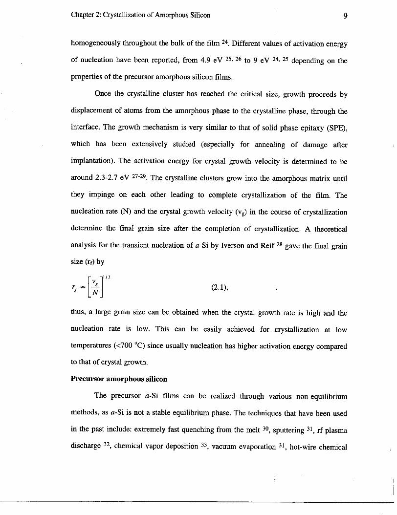
nucleation rate (N) and the crystal growth velocity (v g) in the course of crystallization
determine the final grain size after the completion of crystallization. A theoretical
analysis for the transient nucleation of a-Si by Iverson and Reif 28 gave the final grain
size (rc) by
[ ] 1/3 rf oc -t (2.1),
thus, a large grain size can be obtained when the crystal growth rate is high and the
nucleation rate is low. This can be easily achieved for crystallization at low
temperatures «700 °C) since usually nucleation has higher activation energy compared
to that of crystal growth.
Precursor amorphous silicon
The precursor a-Si films can be realized through various non-equilibrium
methods, as a-Si is not a stable equilibrium phase. The techniques that have been used
in the past include: extremely fast quenching from the melt 3°, sputtering 31, rf plasma
discharge 32, chemical vapor deposition 33, vacuum evaporation 31, hot-wire chemical
II

Chapter 2: Crystallization of Amorphous Silicon 10
vapor deposition 34, and ion implantation 35. In addition to the above-listed methods, a
great deal of work has also been reported in literature 36 on the properties of a-Si
deposited in the presence of hydrogen in order to incorporate H into the structure for the
purpose to terminating the dangling bonds in a-Si. In fact some workers have reported
that hydrogen in hydrogenated amorphous silicon films promotes the crystallization of\
the films and aids in the nucleation process 37. This is explained in terms of reduction of
the grain boundary energy of the crystalline nuclei by hydrogenation. This reduction
facilitates the break-up of a single-crystalline growth front into small crystallites, and
the homogenous nucleation of crystals in an amorphous matrix.
Twinning of SPC films
Common feature of SPC polysilicon films is their very high twin density. These
can be generated upon nucleation of the crystalline clusters 22, 38 or during growth 39. In
a-Si, the 6-membered rings are not organized in chair or boat configurations. Hence,
upon nucleation, depending on the local bonding environment and the local bond angle
distortions of the continuous random network, some rings will go on a chair
configuration, whereas some others will adopt the boat configuration, thus initiating
twinning. However, as shown by Drosd and Washburn 39, twinning can also occur
during growth, upon ledge formation on atomically flat (111) crystallographic planes.
On such planes, a cluster of three atoms is needed to fulfil the criteria of two undistorted
bonds per atom of the crystal phase (or alternatively, to fulfil the criteria of completion
of 6-membered rings). As there are two ways of placing such clusters on the (111)
surface, corresponding to the chair-type or the boat-type, twins are easily created, again
depending on the local bonding environment and bond angle distortions. Also, Drosd
and Washburn have shown that the presence of twins facilitates growth by providing
favorable attachment sites for the atoms of the amorphous phase, at the boundary of the
",;~

Chapter 2: Crystallization of Amorphous Silicon 11
twin with the amorphous matrix. These results in a local growth enhancement, which
tends to favor the formation of extended twin bands. Since in poly-Si, the critical
crystalline clusters, which initiate growth are bounded by (111) planes for energetic
reasons, twinning by the above mechanism is very likely, resulting in the well known
highly twinned structure of the SPC films with grains typically oriented in the (111)
vertical direction 38.
Effect of impurities
The presence of impurities in the a-Si layer, especially at concentrations> 0.1
at. %, can have dramatic effects on the kinetics of solid phase crystallization. Csepregi
et al 40 first showed that group ill and V dopants can greatly increase the rate of SPE,
whereas non-doping impurities like 0, N, and C significantly reduce the SPE rate 41.
Besides, their effects on SPE, impurities can also alter the random nucleation of
crystallites. Yamamoto et al 42 observed that high concentrations of phosphorus reduced
the nucleation rate during experiments on lateral SPE of Si over oxide layers. This
effect of phosphorus on the crystallization kinetics of a-Si films will be discussed
further in Section 3.3.6. When impurity concentrations exceed about 0.3 at. %,
processes such as impurity segregation and precipitation can alter the crystallization
kinetics to the extent that impurities which increase the SPE rate at lower concentrations
can actually retard the rate 43,44. These processes are strongly influenced by the growth
temperature and the rate at which impurities diffuse in the a-Si layer.
2.2.2 Annealing techniques
Furnace and rapid thermal annealing
As mentioned earlier, solid phase crystallization occurs when enough energy is
provided to the atoms in the amorphous phase to rearrange themselves into an ordered
state leading to the crystalline phase. This can be achieved by various techniques, with
["N"~,")j!j
Chapter 2: Crystallization of Amorphous Silicon 12
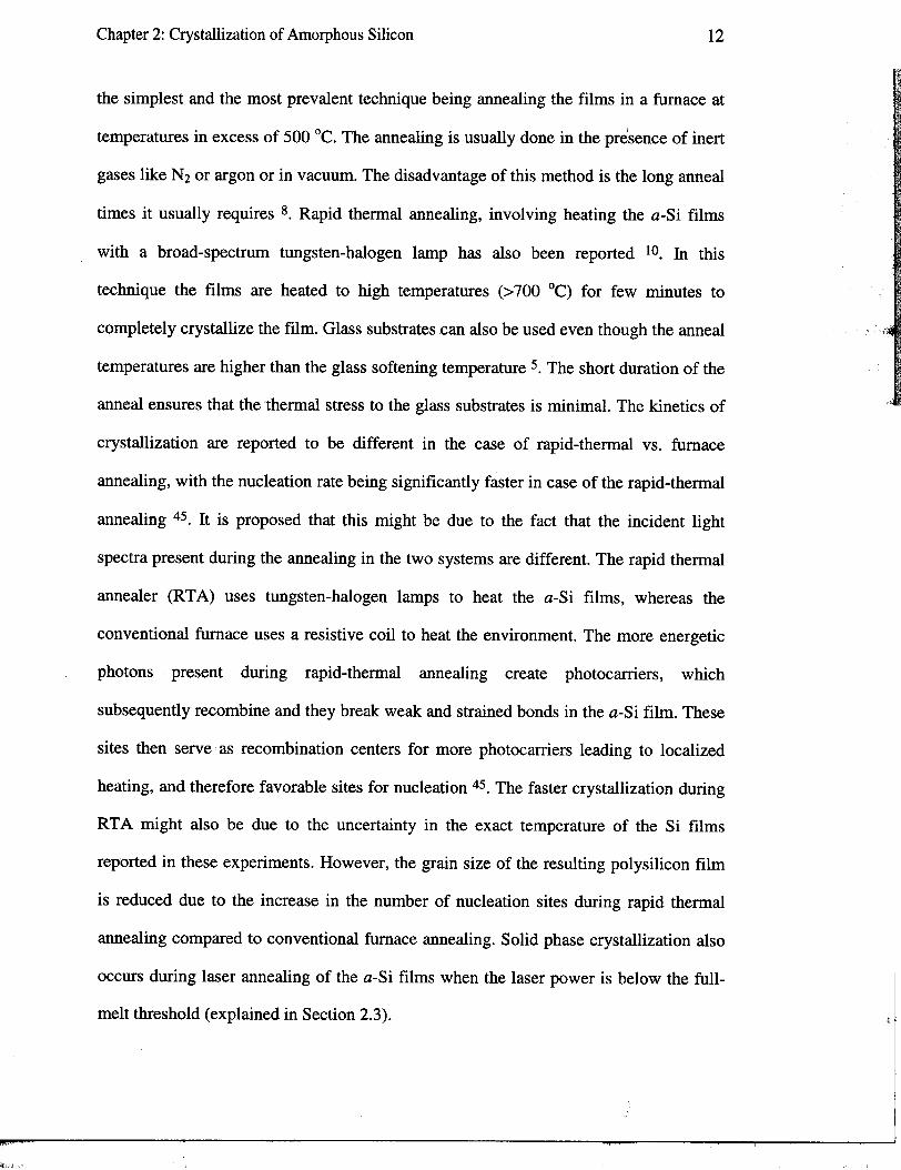
t~the simplest and the most prevalent technique being annealing the films in a furnace at
temperatures in excess of 500 °C. The annealing is usually done in the presence of inert
gases like Nz or argon or in vacuum. The disadvantage of this method is the long anneal
times it usually requires 8. Rapid thermal annealing, involving heating the a-Si films
with a broad-spectrum tungsten-halogen lamp has also been reported 1°. In this
technique the films are heated to high temperatures (>700 °C) for few minutes to
completely crystallize the film. Glass substrates can also be used even though the anneal
temperatures are higher than the glass softening temperature 5. The short duration of the
anneal ensures that the 'thermal stress to the glass substrates is minimal. The kinetics of
crystallization are reported to be different in the case of rapid-thermal vs. furnace
annealing, with the nucleation rate being significantly faster in case of the rapid-thermal
annealing 45. It is proposed that this might be due to the fact that the incident light
spectra present during the annealing in the two systems are different. The rapid thermal
annealer (RT A) uses tungsten-halogen lamps to heat the a-Si films, whereas the
conventional furnace uses a resistive coil to heat the environment. The more energetic
photons present during rapid-thermal annealing create photocarriers, which
subsequently recombine and they break weak and strained bonds in the a-Si film. These
sites then serve as recombination centers for more photocarriers leading to localized
heating, and therefore favorable sites for nucleation 45. The faster crystallization during
RT A might also be due to the uncertainty in the exact temperature of the Si films
reported in these experiments. However, the grain size of the resulting polysilicon film
is reduced due to the increase in the number of nucleation sites during rapid thermal
annealing compared to conventional furnace annealing. Solid phase crystallization also
occurs during laser annealing of the a-Si films when the laser power is below the full-
melt threshold (explained in Section 2.3). "
,",,"~" I" I

Chapter 2: Crystallization of Amorphous Silicon 13
Microwave induced crystallization
Recently Lee at al. 19 have reported the use of microwave heating for the solid
phase crystallization of PECVD a-Si:H films at low temperatures. The microwave
heating (microwave frequency of 2.45 GHz and power of -450 W) lowered the thermal
budget of the crystallization process to a few hours at 550 °c. The hydrogen
outdiffusion was also enhanced during microwave heating compared to conventional
furnace heating, with nearly all the hydrogen in the a-Si:H films out diffused in -20 min
at 400 °c. The crystallization time of the films was also nearly independent of the
growth temperature 'Of the precursor a-Si:H films. In contrast, during conventional
furnace heating, the crystallization time was strongly dependent on deposition
temperature (will be discussed later in Sections 3.3.4 and 6.2.1). It was speculated that
the Si diffusivity is enhanced due the microwave-Si interaction, which might explain
the low-temperature short-time crystallization. The explanation for all the microwave
effects is still unknown, though it is speculated that the microwave enhances transport
of materials 46, 47. The largest grain size reported for polysilicon films obtained by this
technique is -0.78 J.Lm 19. Further work is necessary to understand the microwave effect
in detail and optimize the process to realize larger grain polysilicon films.
2.2.3 Nucleation enhancement techniques
Crystallization of a-Si films on glass by furnace annealing, limited to -600 °c,
requires long anneal times of 20-60 h, depending on the properties of the initial
precursor a-Si film 8. This is not attractive for processing due to reduced throughput.
Nucleation of the silicon crystallites with an activation energy of -5 e V 28 is usually the
rate-limiting step. Various techniques have been tried to hasten the crystallization
process or reduce the crystallization temperature. In the following sections we will
briefly describe the enhancement methods studied.
Chapter 2: Crystallization of Amorphous Silicon 14
Metal-induced crystallization
Metallic impurities in a-Si films lead to reduction of the crystallization
temperature (T c) of the a-Si films, with T c generally decreasing with increasing metal
concentration up to -20 at: % 43. This phenomenon is often referred to as metal-induced
crystallization (MIC). Various metallic impurities like Au, Cu, Fe, In, Ni, Rh, Sn, Pd
and W have been studied. The metal (X) is introduced in the a-Si layers by either ion
implantation 24, or during growth in the form of co-deposited Si-X alloys 48, or by
depositing a thin layer of metal on top of the a-Si layer 10,49 and subsequently annealing
the film.
The explanation offered for the enhanced crystallization is that for those metals
forming eutectics with Si like AI, Au, Sn, Sb, and In, dissolution of metal atoms in a-Si
may weaken the Si-Si bonds and enhance the nucleation and growth of crystalline Si 48.
Tan et al 50 further suggested that the breaking of metastable metal-Si bonds facilitates
the local rearrangement of atoms required for crystallization. On the other hand, for
those metals forming silicides (or reactive metal alloys) like Ni, Pd, Ti, W and Cu, it has
been suggested that the formation of silicides with lattice constants close to that of Si is
a necessary prerequisite for MIC 51. A-Si films can also be selectively crystallized to
realize both amorphous and polycrystalline regions on the same substrate by selectively
depositing thin layer of metal on the a-Si film and annealing them 1°. Selective
deposition of palladium 52 or nickel 53, 54 on a-Si thin films was also found to induce
crystallization outside of the regions covered with metal. This phenomenon has been
called metal-induced lateral crystallization (Mll..C). We will discuss this further in
Section 6.3.3. Transistors made in Mll..C films (seeded through source/drain regions),
had higher field-effect mobilities of -120 cm2Ns compared to -30 cm2Ns for
transistors in unseeded films 53.

Chapter 2: Crystallization of Amorphous Silicon 15
Recently Kuo and Kozlowski 55 have shown that using either nickel or
palladium and pulsed rapid thermal annealing (3 pulses of 1-s 800 °c heating/5-s
cooling), the crystallization time of formation of polysilicon from a-Si can be as small
as a few seconds. However, MIC or MILC can lead to residual metal contamination of
the Si films due to the metal silicides 56,57 or metallic alloys 58.
Germanium-induced crystallization
Germanium, introduced in amorphous Si layers either by ion implantation 59 or
during growth of the film in the form of a-SixGel-x alloys 6°, is known to reduce the
crystallization time of the films and also lead to improvement of the field-effect
mobility of the TFTs made in such films 61. By using Sio.47Geo.53 alloy the
crystallization temperature can be lowered to temperature as low as 500 °c with an
annealing time of -10 h 6°. This is therefore attractive for use as active layers for
fabrication of TFfs for AMLCDs. Ion implantation of Ge+ instead of Si+ to drive the
as-grown polysilicon films amorphous, resulted in decrease of activation energy for
nucleation during the subsequent anneal from 5.9 eV for the pure a-Si films to 4.6 eV
for the Ge + implanted films 59. The crystal growth velocities were also significantly
larger for the Ge+ implanted films 59. The final grain size of the completely crystallized
films was also larger in the case of Ge + implanted films, with undoped Ge + implanted
films achieving grains about 2-3 times larger that Si+ implanted films, depending on the
annealing temperature 59.
Germanium has also been used to achieve lateral crystallization through
localized seeding similar to MILC. Transistors made in such laterally seeded polysilicon
films have field-effect mobilities as high as 300 cm2/Vs compared to -100 cm2/Vs for
the conventional unseeded polysilicon TFfs 62.

Chapter 2: Crystallization of Amorphous Silicon 16
Ion-bearn-induced crystallization
Amorphous Si layers on Si substrates are epitaxially crystallized by ion-beam-
induced epitaxial crystallization (ffimC) at temperatures as low as 150 °C? far below the
500-600 °c temperature of ordinary solid-phase epitaxial growth (SPEG) during furnace
annealing. The rates of ffimC are increased by the amount of inelastic scattering for the
incident mega-electron-volt heavy-ion beam 63. Typically I-MeV Xe ions are implanted
into the a-Si layer at a temperature of -300 °c 64. Ion-beam induced crystallization
(ffiIC) can be used in the formation of SOl structures, as it is a low-temperature
nonequilibrium process. Because ffimC/lBIC occurs at temperatures far below ordinary
SPEG temperatures, using irradiation at temperatures below 300 °c can prevent the
crystallization of a Si layer on the SiO2 film in non-irradiated areas.
The crystallization rate in ffimC is controlled by defects in the amorphous layer
like dangling bonds 65, kinks 66, or vacant spaces 67 produced at the
amorphous/crystalline (a/c) interface by the nuclear scattering of the incident ions. The
random-network structure a-Si does not reconstruct to the crystal structure until it is
annealed at 500-600 °c, but the "vacant spaces" in the a-Si layer near the a/c interface
might induce crystallization at temperatures below 450 °c. The vacant spaces make the
Si atoms vibrate more freely. When dangling bonds are formed by the desorption of1hydrogen atoms in the a-Si films during the furnace annealing at low temperatures, ,
reconstruction of Si atoms occurs, inducing the movement of interstitial Si atoms to the
vacant spaces, hence resulting in the low-temperature crystallization 64. Jackson 65
reported that the crystallization could also occur through dangling bonds without the
help of vacant spaces. The formation of dangling bonds (after hydrogen desorption or
after the ion implantaion) may directly result in the reconstruction of Si atoms to the
crystal structure at low temperature. This technique is still being actively studied to
-

Chapter 2: Crystallization of Amorphous Silicon 17
optimize the conditions so as to achieve large grain silicon i on insulating layers.
However, the heavy ion implantation process in ffiIC/ffiIEC can lead to damage to the
pre-existing devices if used for 3D ICs.
Plasma-induced crystallization
In addition to the above-mentioned techniques to enhance the nucleation rate
and thereby the crystallization kinetics of a-Si films, recently it was shown that, plasma
treatment of hydrogenated amorphous silicon films (a-Si:H) deposited by plasma
enhanced chemical vapor deposition resulted in enhancement of the crystallization rate
of the film during subsequent anneal. The plasma treatment using either oxygen 68-71,
helium 68, 72 or hydrogen 68 was conducted in an electron cylcotron resonance (ECR)
plasma system at a substrate temperature of -400 °c for 1 h. During the subsequent
anneal of the films in a furnace, it was found that films exposed to the plasma prior to
the anneal crystallized faster compared to the untreated films. It was found that
hydrogen and helium plasmas had the most drastic effect on the crystallization rates of
a-Si:H films with crystallization time of only 6 h at 600 °c compared to 32 h for the
untreated film. Oxygen plasma treatment resulted in reducing the crystallization time to
-17 h 72. We found that room-temperature radio frequency (RF) hydrogen plasma
treatment resulted in reduction of crystallization time ofa-Si:H films from -20 h to -4 h
at 600 °c 73,74. In addition, it was also found that the plasma effect could be masked
using a hard mask like SiO2, and hence be used to create both polycrystalline and
amorphous regions in the same single silicon layer 68, 71, 72. However, others gave no
clear explanation for this enhancement effect.
Conde et al12 have found that rf or ECR hydrogen plasma treatment at substrate
temperature of 300 °c of hot-wire deposited a-Si:H films resulted in reduction in the
threshold power of the laser needed to induce crystallization. ECR hydrogen plasma
'"c 1""""'1

Chapter 2: Crystallization of Amorphous Silicon 18
treatment resulted in the least threshold laser power. In fact ECR hydrogen plasma
treatment with -200 V DC bias applied to the sample during the treatment had the most
drastic effect, indicating that the plasma effect is strongly dependent on the hydrogen
ion energy during treatment. It was proposed that the hydrogen plasma treatment at 300
i°C resulted in structural changes in the hot-wire a-Si:H resulting in reduction of the 1
laser power required to induce crystallization. These structural changes, however, did
not change the transport properties of the films 12. ,
Plasma-enhanced crystallization of a-Si:H might be the technique that
introduces the least contamination in the films compared to either metal-induced or 1
germanium~induced crystallization of a-Si. The radiation damage is also minimal in this
technique compared to ion-be am-induced crystallization. In our work, we studied the
plasma-enhancement effect further, especially the effect of hydrogen plasma treatment
on the crystallization of hydrogenated amorphous silicon films.
2.3 LASER CRYSTALLIZATION
Techniques of laser annealing of amorphous silicon, especially by using an I
excimer laser, have been widely reported over the past decade, with commercial interest
focused on producing high-speed, low-temperature, TFTs for large electronics and for
3-D ICs. Laser annealing was first used to activate ion-implanted dopants in crystalline-
Si and remove the corresponding lattice damage 75. During irradiation of semiconductor
materials with photons of energy hv > Egap (where Egap is the energy gap of the
semiconductor), absorption of the laser energy takes place by the excitation of electron-
hole pairs across the gap. After a rapid thermal equilibration of the photoexcited carrier
system (-10-14 s), the energy is transferred to the lattice by phonon emission, on a
picosecond time scale II,

Chapter 2: Crystallization of Amorphous Silicon 19
For the particular case of a-Si irradiation by UV wavelength lasers (e.g. excimer
laser pulse duration of't -30 ns), the absorption depth of the laser is of the order of 10-6
cm and the heat diffusion length in a-Si over the pulse duration, (D't)1/2 (D is the
thermal diffusivity in a-Si), amounts to -10-5 cm at elevated temperature 76. In these
conditions, most of the energy deposited during the laser pulse will be localized within
the first 100 nm of the irradiated film, whereas the underlying substrate will remain
nearly unheated.
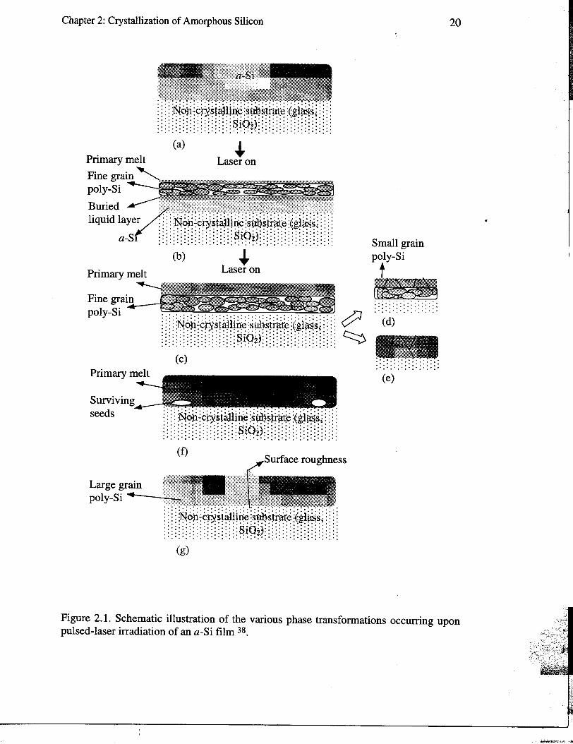
Fig. 2.1 38 schematically shows the various transformations that can occur upon
pulsed-laser irradiation of a-Si films with pulse duration of 30-50 ns. The melting
temperature of a-Si is about 225 °c below that of c-Si 77, therefore under normal
heating conditions a-Si crystallizes before its melts. However, under pulsed-laser
heating, the heat supply is too fast and the crystallization is bypassed, so a-Si is directly
melted by a first order phase transformation. As a consequence the liquid-Si (I-Si) can
be severely undercooled relative to the equilibrium melting temperature of c-Si. If the
undercooling is maintained long enough, nucleation can occur in the I-Si, which can
trigger explosive crystallization of the underlying a-Si 77 (Fig. 2.1(b». The liquid layer
propagates downward due to the latent heat of crystallization melting the adjoining a-Si,
leaving behind fine grain polysilicon (Fig. 2.I(c» 78. Later in the laser pulse, the buried
liquid layer has permeated throughout the film, and the primary melt front penetrates
the fine grain region remelting it (Fig. 2.I(e». However, if the laser energy density is
not high enough, this remelting will not occur and the film solidifies leading to fine
grain polysilicon (Fig. 2.I(d». If, on the other hand, the fine grain region is completely
melted and the liquid allowed to cool down after the end of the laser pulse,
undercooling again occurs and homogenous nucleation takes place in the melt, leading
to small grain polysilicon (Fig. 2. 1 (e» 38. When the laser energy density is such that the
,~
Chapter 2: Crystallization of Amorphous Silicon 20,
: :. .. .""': .
~ ~ ~ ~ ~~~f~o/~t#~~¥ :~~~~~!~~ ~~~~~~~ ~ j ~ j
~ ~ ~ ~ ~ ~ ~ ~ ~ ~ ~ ~ ~ ~ ~ ~ ~ ~ ~ ~ ~ ~~?~J~ ~ ~ ~ ~ ~ ~ ~ ~ ~ ~ ~ ~ ~ ~ ~ ~ ~ ~ ~ ~
(a) -+Primary melt Laser onFine grain'poly-SiBuriedliquid layer ~ ~ ~: :*~~f~~~t~~~~#~~~~~~~~~~~~~~~ ~::: .
a-SI ~ ~ ~ ~ ~ ~ ~ ~ ~ ~ ~ ~ ~ ~ ~ ~ ~ ~ ~ ~ ~~~?~J~ ~ ~ ~: ~ ~ ~ ~ ~ ~ ~ ~ ~ ~ ~ ~ ~~~ ~ Small grain
(b) -+ poly-Si !P . It Laser on .
nmary me I
Fine g~ain ::::::::::::::::::POly-Sl . . . . . . . . . . . . . . . . . . . . . . . .. ...,>:] : ~ : : :N6ri~~iY~iitiiiii6 :~f1b~i~~~ :(~i~~: ~: :: V' (d)
~~~:(~)~~~~~~~~~~~~~~~q~~~~~~~~~~~~~~~~~:1j:~: ~ -:Primary (e)
Survivingseeds j : : : :*~~f~~~t~~~# ~~~~~~~~ ~~~~~~~ ~ ~ : :
~ ~ : ~ : ~ ~ : ~ ~ ~ ~ ~ ~ ~ ~ ~ ~ ~ ~ ~ ~~?~J~ ~ ~ ~ ~ ~ ~ ~ ~ ~ ~ ~ ~ ~ ~ ~ ~ ~ : ~ :
(f) roughness
Large gpoly-Si ;;; ~ : ~ : ~~~~f~o/~t#~~¥ :~~~~~!~~ ~~~~~~~: ~ ~ ~
~ ~ ~ ~ ~ ~ ~ ~ ~ ~ ~ ~ ~ ~ ~ ~ ~ ~ ~ ~ ~ ~~?~J~ ~ ~ ~ ~ ~ ~ ~ ~ ~ ~ ~ ~ ~ ~ ~ ~ ~ ~ ~ :
(g)
Figure 2.1. Schematic illustration of the various phase transformations occurring uponpulsed-laser irradiation of an a-Si film 38.
II
-""'c,,,'"

Chapter 2: Crystallization of Amorphous Silicon 21
fine grain polysilicon obtained after the explosive crystallization is not totally melted
and some seeds survive, large grains are obtained due to crystal growth from the
surviving seeds (Figs. 2.1(f) and (g)). This regime of grain growth is referred to as
super-lateral growth (SLG) 79.
The SLG regime corresponds to a narrow processing window requiring very
good beam uniformity and pulse to pulse reproducibility. For large area processing,
sophisticated beam homogenizers that can cost more than the laser, are required. Beam
overlap region during scanning is another source of nonuniformity, since at the edges
there is always an energy gradient. Pulsed laser crystallization also leads to surface
roughness with a high density of protuberances, especially where the grains meet 8°.
In spite of all these drawbacks, there is active interest nowadays to develop this
technology further. Kim and 1m 81 have obtained large elongated grains with almost
parallel grain boundaries using lateral thermal gradients established through the use of
patterned antireflective strips (of SiO2 or Si3N4), which modulate the absorption of the
laser energy. 1m and Sposili 82 have recently obtained high quality Si films by J
sequential lateral solidification. 1m and Song 16 have used artificially controlled super
I
lateral growth and used the high-substrate temperature liquid-to-solid transformation .j
characteristics, in order to realize patterned single-crystal islands (-50x50 flm1 on
oxidized Si wafer. TFTs have been made in laser annealed films with field-effect
mobilites, close to .that of single-crystal silicon, of 640 cm2Ns for n-channel TFTs and
400 cm2Ns for p-channel TFTs 83. Several groups are actively working to optimize the
laser annealing process and improve material properties of the crystalline Si films and
thereby improve device characteristics."!
I;, !c.c,~.

Chapter 2: Crystallization of Amorphous Silicon 22
2.4 ZONE-MELTING RECRYSTALLIZATION
The predominant method of crystallization of a-Si being studied involve either
furnace or rapid thermal or laser annealing to achieve the objectives stated in the
introduction of this chapter. Each technique has its unique advantage and on the flip
side there are still many drawbacks yet to be overcome. In addition to the above-
mentioned crystallization methods, zone-melting crystallization has long been studied to
obtain SOl structures.
Zone-melting recrystallization (ZMR) involves heating the SOl wafer by a
moving (graphite strip) heat source. Oxidized Si substrates are used typically with the
polysilicon film to be recrystallized capped with SiOz during ZMR. In the typical ZMR
process the sample is placed in a water-cooled chamber that surrounds the heating
elements (bottom heater and graphite strips). The chamber is filled with inert gas such
as helium or argon. In some cases there is continuous flow of the inert gases. All three
heat transfer modes (conduction, convection, and radiation) play roles of varying
significance. The film structure to be recrystallized is generally placed on the lower
heater that raises the temperature of the wafer to just below the melting point of silicon.
The graphite strip heats the topside of the wafer and establishes a narrow molten zone in
the silicon film to be recrystallized. The graphite strip is then slowly moved across the
surface of the material. As the silicon film freezes behind the strip, a single crystal
forms 18.
The crystal growth strongly depends on the control of the temperature profile
within the silicon 84. Depending on the width of the melt-zone, varying qualities of
films are developed 18. The most common imperfections found in films processed by
ZMR are low-angle"sub-grain boundaries (subboundaries). Dislocation trails or clusters
are also common. Subboundaries are defined as defects that exhibit a crystallographic
p.-- '-
Chapter 2: Crystallization of Amorphous Silicon 23
angular misalignment on the order of 1 ° from the growth axis 85. Various combinations
of low scan speeds with low thermal gradients produced subboundary free SOl
structures 84. TFfs made in such films had excellent characteristics with mobilities of
-420 cm2Ns for n-channel transistors on quartz substrates 86. However, the ZMR is a
high-temperature process. The surface of the substrate heats up to a few degrees lower
than Si melting temperature (-1400 °C) for several seconds 87, and is not suitable for
glass substrates and for 3-D ICs fabrication.
2.5 SUMMARY
Polycrystalline silicon films obtained from crystallization of precursor
amorphous silicon films are shown to have superior material properties compared to as-
grown polysilicon. We have discussed the several methods that have been used to"
crystallize amorphous silicon films and reviewed the techniques used to enhance the
crystallization process. The more widely used techniques of solid phase crystallization
and pulsed-laser crystallization have been discussed in greater detail with the
advantages and drawbacks of each technique highlighted.
In the next chapter, we will explicate the solid phase crystallization of
hydrogenated amorphous silicon films deposited by plasma-enhanced chemical vapor
deposition, with emphasis on the hydrogen-plasma-enhancement effect. We will then
report on the use of this effect to improve the performance of polysilicon transistors
(chapter 4) and on the integration of polysilicon and amorphous silicon transistors on
the substrate (chapter 5). The final goal is to realize close to single crystal silicon films
on insulating substrates at low temperature. In chapter 6 we will discuss the methods
that have been tried by others to achieve this and cover issues such as grain
enlargement, control of grain orientation, and reduction of defects within the grains.
"","" ~~I : I
Chapter 2: Crystallization of Amorphous Silicon 24
REFERENCES
[1] T. Morita, S. Tsuchimoto, and N. Hashizume, "The low temperature polysilicon TFTtechnology for manufacturing of active matrix liquid crystal displays," MaterialsResearch Society Symposium Proceedings, vol. 345, pp. 71-80, 1994.
[2] A. G. Lewis, I.-W. Wu, T. Y. Huang, A. Chiang, and R. H. Bruce, Technical Digest ofInternational Electron Devices Meeting, pp. 843-846, 1990.
[3] S. D. S. Malhi, H. Shichijo, S. K. Banerjee, R. Sundaresan, M. Elahy, G. P. Pollack, W.F. Richardson, A. H. Shah, L. R. Hite, R. H. Womack, P. L. Chatterjee, and H. W. Lam,"Characteristics and three-dimensional integration of MOSFET's in small-grain LPCVDpolycrystalline silicon," IEEE Transactions on Electron Devices, vol. 32, pp. 258-281,1985.
[4] K. T.-Y. Kung and R. Reif, Journal of Applied Physics, vol. 62, pp. 1985, 1987.[5] D. M. Moffatt, "Properties of glass substrates for poly-Si AMLCD technology,"
Materials Research Society Symposium Proceedings, vol. 377,pp. 871-876, 1995.[6] M. Ino, J. Miyano, H. Kurogi, Y. Nagatomo, and M. Yoshimaru, "Rugged surface
polycrystalline silicon film deposition and its application in a stacked dynamic randomaccess memory capacitor electrode," Journal of Vacuum Science and Technology B,vol. 14, pp. 751-756, 1996.
[7] H. C. Lin, H. Y. Lin, C. Y. Chang, T. F. Lei, P. J. Wang, and C. Y. Chao, AppliedPhysics Letters, vol. 63, pp. 1351, 1993.
[8] M. K. Hatalis and D. W. Greve, "Large grain polycrystalline silicon by low temperatureannealing of low-pressure deposition amorphous silicon films," Journal of AppliedPhysics, vol. 63, pp. 2260-2266, 1988.
[9] R. Kakkad, J. Smith, W. S. Lau, and S. J. Fonash, "Crystallized films by lowtemperature rapid thermal annealing of amorphous silicon," Journal of Applied Physics,vol. 65, pp. 2069-2072, 1989.
[10] G. Liu and S. J. Fonash, "Selective area crystallization of amorphous silicon films bylow-temperature rapid thermal annealing," Applied Physics Letters, vol. 55, pp. 660-662, 1989.
[11] R. F. Wood and G. E. Jellison, Pulsed Laser Processing of Semiconductors, vol. 23:Academic Press, 1984.
[12] J. P. Conde, P. Brogueira, and V. Chu, "Post-deposition annealing and hydrogenation ofhot-wire amorphous and microcrystalline silicon films," Materials Research SocietySymposium Proceedings, vol. 452, pp. 779-784, 1997.
[13] D. Toet, B. Koopmans, P. V. Santos, R. B. Bergmann, and B. Richards, "Growth ofpolycrystalline silicon on glass by selective laser-induced nucleation," Applied PhysicsLetters, vol. 69, pp. 3719-3721, 1996.
[14] S. D. Brotherton, D. J. McCulloch, J. P. Gowers, and A. Gill, "Laser crystallized poly-Si TFTs," Microelectronic Engineering, vol. 19, pp. 101-104, 1992.
[15] T. Sameshima, S. Usui, and M. Sekiya, "XeCI excimer laser annealing used in thefabrication of poly-Si TFTs," IEEE Electron Device Letters, vol. 7, pp. 276-278, 1986.
[16] H. J. Song and J. S. Im, "Single-crystal Si islands on SiO2 obtained via excimer-laserirradiation of a patterned Si film," Applied Physics Letters, vol. 68, pp. 3165-3167,1996.
[17] M. D. Efremov, V. V. Bolotov, V. A. Volodin, L. I. Fedina, and E. A. Lipatnikov,"Excimer laser and rapid thermal annealing stimulation of solid-phase nucleation andcrystallization in amorphous silicon films on glass substrates," Journal of Physics:Condensed Matter, vol. 8, pp. 273-286, 1996.
~;i
c.c.CC--~~::~='.

Chapter 2: Crystallization of Amorphous Silicon 25
[18] I. N. Miaoulis, P. Y. Wong, S. M. Yoon, R. D. Robinson, and C. K. Hess, "Thermalanalysis of zone-melting recrystallization of silicon-on-insulator structures with aninfrared heat source: An overview," Journal of Electrochemical Society, vol. 139, pp.2687-2696, 1992.
[19] J. N. Lee, Y. W. Choi, B. J. Lee, and B. T. Ahn, "Microwave-induced low-temperaturecrystallization of amorphous silicon thin films," Journal of Applied Physics, vol. 82, pp.2918-2921, 1997.
[20] J. Nakata, "Epitaxial crystallization during 600 °C furnace annealing of amorphous Silayer deposited by low-pressure chemical-vapor deposition and irradiated with 1 MeVXe ions," Journal of Applied Physics, vol. 82, pp. 5446-5459, 1997.
[21] E. P. Donovan, F. Spaepan, D. Turnbull, J. M. Poate, and D. C. Jacobson, Journal ofApplied Physics, vol. 57, pp. 1795, 1985.
[22] R. Sinclair, J. Morgiel, A. S. Kirtikar, I. W. Wu, and A. Chiang, Ultramicroscopy, vol.51, pp. 41, 1993.
[23] M.-K. Ryu, S.-M. Hwang, T.-H. Kim, K.-B. Kim, and S.-H. Min, "The effect of surfacenucleation on the evolution of crystalline microstructure during solid phasecrystallization of amorphous Si films on SiO2," Applied Physics Letters, vol. 71, pp.3063-3065, 1997.
[24] G. L. Olson and J. A. Roth, "Kinetics of solid phase crystallization in amorphoussilicon," Materials Science Reports, vol. 3, pp. 3-77, 1988.
[25] K. Zellama, P. Germain, S. Squelard, J. C. Bourgoin, and P. A. Thomas,"Crystallization in amorphous silicon," Journal of Applied Physics, vol. 50, pp. 6995-7000, 1979.
[26] U. Koster, Physica Status Solidi A, vol. 48, pp. 313,1978.[27] L. Csepregi, E. F. Kennedy, J. W. Mayer, and T. W. Sigmon, "Substrate-orientation
dependence of the epitaxial regrowth rate from Si-implanted amorphous Si," Journal ofApplied Physics, vol. 49, pp. 3906-3911,1978.
[28] R. B. Iverson and R. Reif, "Recrystallization of amorphized polycrystalline siliconfilms on SiO2: Temperature dependence of the crystallization parameters," Journal ofApplied Physics, vol. 62, pp. 1675-1681, 1987.
[29] C. Licoppe and Y. I. Nissim, Journal of Applied Physics, vol. 59, pp. 432, 1986.[30] P. L. Liu, R. Yen, N. Bloemberg, and R. T. Hodgson, Applied Physics Letters, vol. 34,
pp. 864, 1979.[31] M. H. Brodsky, R. S. Title, K. Weiser, and G. D. Pettit, Physical Review B, vol. 1, pp.
2639, 1970.[32] W. E. Spear and P. G. LeComber, Phil. Mag., vol. 33, pp. 1976, 1976.[33] T. I. Kamins, M. M. Mandurah, and K. C. Saraswat, Journal of Electrochemical
Society, vol. 125, pp. 927, 1978.[34] H. Wiesmann, A. K. Ghosh, T. McMahon, and M. Strongin, Journal of Applied
Physics, vol. 50, pp. 3752, 1979.[35] J. W. Mayer, L. Eriksson, and J. A. Davies, Ion Implantation in Semiconductors. New
York: Academic Press, 1970.[36] J. D. Joannnopoulus and G. Lucovsky, "The Physics of Hydrogenated Amorphous
Silicon n," Berlin: Springer, 1984.[37] S. Wagner, S. H. Wolff, and J. M. Gibson, "The role of hydrogen in silicon
microcrystallization," Materials Research Society Symposium Proceedings, vol. 164,pp. 161-170, 1990.
[38] D. Pribat, P. Legagneux, F. Plais, C. Reita, F. Petinot, and 0. Huet, "Low temperaturepolysilicon materials and devices," Materials Researc;-h Society SymposiumProceedings, vol. 424, pp. 127-139, 1997.
Ci;'"'c,»~,,~

Chapter 2: Crystallization of Amorphous Silicon 26
[39] R. Drosd and J. Washburn, Journal of Applied Physics, vol. 53, pp. 397,1982.[40] L. Csepregi, E. F. Kennedy, T. J. Gallagher, J. W. Mayer, and T. W. Sigmon, Journal of
Applied Physics, vol. 48, pp. 4234, 1977.[41] E. F. Kennedy, L. Csepregi, J. W. Mayer, and T. W. Sigmon, "Influence of 160, 12C,
14N, and noble gases on the crystallization of amorphous Si layers," Journal of AppliedPhysics, vol. 48, pp. 4241-4246,1977.
[42] H. Yamamoto, H. Ishiwara, and S. Furukawa, Applied Physics Letters, vol. 46, pp. 268,1985.
[43] J. R. A. Carlsson, J.-E. Sundgren, X.-H. Li, L. D. Madsen, and H. T. G. Hentzell,"Predicting the crystallization temperature variation with composition for amorphoussilicon-based binary alloy thin films," Journal of Applied Physics, vol. 81, pp. 1150-1156, 1997.
[44] J. S. Williams and R. G. Elliman, Applied Physics Letters, vol. 40, pp. 266, 1982.[45] R. Kingi, Y. Wang, S. J. Fonash, O. Awadelkarim, J. Mehlhaff, and H. Hovagimian,
"Comparison between rapid thermal and furnace annealing for a-Si solid phasecrystallization," Materials Research Society Symposium Proceedings, vol. 424, pp. 237-241, 1997.
[46] J. H. Brooske, R. F. Cooper, and I. Dobson, Journal of Materials Research, vol. 7, pp.495, 1992.
[47] M. A. Janney, H. D. Kimrey, M. A. Schimiat, and J. O. Kiggan, Journal of AmericanCeramic Society, vol. 74, pp. 1675, 1991.
[48] G. Radnoczi, A. Robertsson, H. T. G. Hentzell, S. F. Gong, and M.-A. Hasan, "AIinduced crystallization of a-Si," Journal of Applied Physics, vol. 69, pp. 6394-6399,1991.
[49] H. Kim, J. G. Couillard, and D. G. Ast, "Kinetics of silicide-induced crystallization ofpolycrystallization thin-film transistors fabricated from amorphous chemical-vapordeposition silicon," Applied Physics Letters, vol. 72, pp. 803-805, 1998.
[50] Z. Tan, S. M. Heald, M. Rapposch, C. E. Bouldin, and J. C. Woicik, Physical Review E,vol. 46, pp. 9505, 1992.
[51] C. Hayzelden, J. L. Batstone, and R.. C. Cammarata, Applied Physics Letters, vol. 60,pp. 225, 1992.
[52] S.-W. Lee, Y.-C. Jeon, and S.-K. Joo, Applied Physics Letters, vol. 66, pp. 1671, 1995.[53] S.-W. Lee, T.-H. Ihn, and S.-K. Joo, "Low-temperature dopant activation and its
application to polycrystalline silicon thin film transistors," Applied Physics Letters, vol.69, pp. 380-382, 1996.
[54] S.-W. Lee and S.-K. Joo, "Low temperature poly-Si thin-film transistor fabrication bymetal-induced lateral crystallization," IEEE Electron Device Letters, vol. 17, pp. 160-162, 1996.
[55] Y. Kuo and P. M. Kozlowski, "Polycrystalline silicon formation by pulsed rapidthermal annealing of amorphous silicon," Applied Physics, vol. 69, pp. 1092-1094,1996.
[56] Z. Jin, G. A. Bhat, M. Yeung, H. S. Kwok, and M. Wong, "Nickel inducedcrystallization of amorphous silicon films," Journal of Applied Physics, vol. 84, pp.194-200, 1998.
[57] S. Y. Yoon, K. H. Kim, C. O. Kim, J. Y. Oh, and J. Jang, "Low temperature metalinduced crystallization of amorphous silicon using a Ni solution," Journal of AppliedPhysics, vol. 82, pp. 5865-5867,1997.
[58] S. F. Gong, H. T. G. Hentzell, A. E. Robertsson, L. Hultman, S.-E. Hornstrom, and G.Radnoczi, "AI-doped and Sb-doped polycrystalline silicon obtained by means of metal-induced crystallization," Journal of Applied Physics, vol. 62, pp. 3726-3732, 1987.

Chapter 2: Crystallization of Amorphous Silicon 27
[59] M. K. Kang, K. Akashi, T. Matsui, and H. Kuwano, "Recrystallization characteristics ofpolycrystalline silicon film amorphized by germanium ion implantation," Solid-StateElectronics, vol. 38, pp. 383-387,1995.
[60] C.-W. Hwang, M.-K. Ryu, K.-B. Kim, S.-C. Lee, and C.-S. Kim, "Solid phasecrystallization of amorphous Si 1-xGex films deposited on SiO2 by molecular beamepitaxy," Journal of Applied Physics, vol. 77, pp. 3042-3047, 1995.
[61] T.-J. King, K. C. Saraswat, andJ. R. Pfiester, IEEE Electron Device Letters, vol. 12, pp.584, 1991.
[62] V. Subramanian and K. C. Saraswat, "High-performance germanium-seeded laterallycrystallized TFT's for vertical device integration," IEEE Transactions on ElectronDevices, vol. 45, pp. 1934-1939, 1998.
[63] J. Nakata, Journal of Applied Physics, vol. 80, pp. 4237, 1996.[64] J. Nakata, "Enhanced crystallization of amorphous Si containing hydrogen without
oxygen during ion-beam irradiation at 310oC and during furnace annealing below450oC," Journal of Applied Physics, vol. 82, pp. 5433-5445, 1.997.
[65] K. A. Jackson, Journal of Materials Research, vol. 3, pp. 1218, 1988.[66] F. Priolo,C. Spinella, and E. Rimini, Physical Review B, vol. 41, pp. 5235, 1990.[67] J. Nakata, Physical Review B, vol. 43, pp. 14643, 1991.[68] S. J. Fonash and A. Yin, "Enhanced crystallization of amorphous films," US Patent No.
US5624873, 1995.[69] A. Yin and S. J. Fonash, "Oxygen plasma enhanced crystallization of a-Si for low
thermal budget poly-Si TFTs on Corning 7059 glass," International Electron DeviceMeeting Technical Digest, pp. 397-400, 1993.
[70] A. Yin and S. J. Fonash, "Oxygen-plasma-enhanced crystalli~tion of a-Si:H films onglass," Journal of Vacuum Science and Technology, vol. A. 12, pp. 1237-1240, 1994.
[71] A. Yin and S. J. Fonash, "Selective Crystallization of a-Si:H films on glass," MaterialsResearch Society Symposium Proceedings, vol. 321, pp. 683-688, 1994.
[72] A. Yin, S. J. Fonash, D. M. Reber, Y. M. Li, and M. Bennett, "A comprehensive studyof plasma enhanced crystallization of a-Si:H films on glass," Materials ResearchSociety Symposium Proceedings, vol. 345, pp. 81-86, 1994.
[73] K. Pangal, J. C. Sturm, S. Wagner, and T. H. Buyuklimanli, "Hydrogen plasma-enhanced crystallization of hydrogenated amorphous silicon films," Journal of AppliedPhysics, vol. 85, pp. 1900-1906, 1999.
[74] K. Pangal, J. C. Sturm, and S. Wagner, "Hydrogen plasma-enhanced crystallization ofamorphous silicon for low temperature polycrystalline silicon TFT's," InternationalElectron Devices Meeting Technical Digest, pp. 371-374, 1998.
[75] E. I. Shtyrkov, I. B. Khaibullin, M. M. Zaripov, M. F. Galyatudinov, and R. M.Bayazitov, Soviet Physics Semiconductors, vol. 9, pp. 1309, 1976.
[76] T. Sameshima, M. Hara,and S. Usui, Japanese Journal of Applied Physics Part 2, vol.28, pp. L2131, 1989.
[77] M. O. Thompson, G. J. Galvin, J. W. Mayer, P. S. Peercy, J. M. Poate, D. C. Jacobson,A. G. Cullis, and N. G. Chew, Physical Review Letters, vol. 52, pp. 2360,1984.
[78] R. F. Wood and G. A. Geist, Physical Review Letters, vol. 57, pp. 873, 1986.[79] J. S. 1m, H. J. Kim, and M. O. Thompson, Applied Physics Letters, vol. 63, pp. 1969,
1993.[80] D. H. Lowndes, S. J. Pennycook, R. F. Wood, G. E. Jellison, and S. P. Withrow,
Materials Research Society Symposium Proceedings, vol. 2, pp. 648, 1986.[81] H. J. Kim and J. S. 1m, Applied Physics Letters, vol. 68, pp. 1513, 1996.[82] J. S. 1m and R. S. Sposili, Materials Research Society Bulletin, vol. 21, pp. 39, 1996.
- - j
-,

Chapter 2: Crystallization of Amorphous Silicon 28
[83] A. Kohno, T. Sameshima, N. Sano, M. Sekiya, and M. Hara, "High performance poly-Si TFTs fabricated using pulsed laser annealing and remote plasma CVD with lowtemperature processing," IEEE Transactions on Electron Devices, vol. 42, pp. 251-256,1995.
[84] L. Pfeiffer, A. E. Gelman, K. A. Jackson, K. W. West, and J. L. Batstone, AppliedPhysics Letters, vol. 51, pp. 1256, 1987.
[85] M. W. Geis, H. I. Smith, D. J. Silversmith, and R. W. Mountain, Journal ofElectrochemical Society, vol. 130, pp. 1178, 1983.
[86] S.-W. Lee, S.-K. Joo, B.-I. Lee, and I.-G. Lim, "Electrical performance of an n-channelTFT fabricated on a quartz substrate by ZMR," Materials Research Society SymposiumProceedings, vol. 424, pp. 153-158, 1997.
[87] M. Robinson, D. J. Lischner, and G. K. Celler, " Large area recrystallization of
polysilicon with tungsten-halogen lamps," Journal of Crystal Growth, vol. 63, pp. 484-492, 1983.

Chapter 3
ENHANCEMENT OF CRYST ALLIZA TION
OF HYDROGENATED AMORPHOUSi
SILICON BY A HYDROGEN PLASMA
ITREATMENT
3.1 INTRODUCTION
Polycrystalline silicon (polysilicon) fornled by the solid phase crystallization of
amorphous silicon (a-Si), as discussed in chapter 2, has far superior material and
electronic properties than as-deposited polysilicon due to the larger grains and smooth
surfaces. Crystallization done by furnace annealing at 600 °c usually requires long
anneal times of the order of 20-60 h 1. In chapter 2, we discussed the various techniques
that have been used to reduce the annealing time, including metal-induced
crystallization (MIC) 2-4, gernlanium-induced crystallization 5-7, and plasma-enhanced
crystallization. The plasma treatment involved exposure of hydrogenated amorphous
silicon (a-Si:H) to either electron cyclotron resonance (ECR) oxygen, hydrogen, and
helium plasmas at 400 °c 8-13, or room-temperature radio frequency (RF) hydrogen
plasma 14-16. It has also been shown that RF or ECR hydrogen plasma treatment at a
substrate temperature of 300 °c of hot-wire deposited a-Si:H films reduces the
"'JC
Chapter 3: Enhancement of crystallization of hydrogenated amorphous silicon by a 30hydrogen plasma treatment
threshold laser power for the subsequent crystallization of the films 17. We will further
study the plasma enhancement technique in this chapter as it introduces the least
potential contamination in the films, while the other crystallization enhancement
techniques can lead to metal or germanium contamination of the films respectively.
As discussed in chapter 2, solid phase crystallization (SPC) of amorphous
silicon (a-Si) involves two distinct processes, namely the nucleation of seeds (formation
of clusters of crystalline silicon) and their growth to polycrystalline films. The rate-
limiting step of the crystallization process is the rate of nucleation of seeds (rn), which
has an activation energy of about 5 eV 18, while the rate of crystal growth (v g) has an
activation energy of about 2.7 eV 18,19. In this chapter we will show that the plasma
treatment hastens the crystallization, and we suggest that this is due to the creation of
seed nuclei. Hence the crystallization comprises only the growth of crystal from these
seeds. Section 3.2 details the experimental procedures followed in this work. The effect
of the precursor a-Si:H film growth and subsequent anneal conditions, and the material
characteristics of the resulting polycrystalline films will be discussed in Section 3.3. In
Section 3.4, the mechanism of seeding by the hydrogen plasma will be analyzed.
Section 3.5 discusses the oxygen-plasma-enhancement effect and finally a summary is
presented in the last section, Section 3.6.
3.2 EXPERIMENTAL PROCEDURE
3.2.1 Substrate preparation, a-Si:H film growth, and characterization methods
Undoped hydrogenated amorphous silicon (a-Si:H) films of thickness from 75 to I
400 nm were deposited on pre-annealed Coming 7059/1737 glass substrates or oxidized
silicon substrates by plasma-enhanced chemical-vapor deposition (PECVD) in a multi-
chamber system (S900) designed by Solarex and Innovative Systems. A schematic
layout of the deposition is illustrated in Fig. 3.1. The system consists of four v~cuum
~".iI'C'(I' ~,,~;~!

Chapter 3: Enhancement of crystallization of hydrogenated amorphous silicon by a 31hydrogen plasma treatment
chambers: the i-chamber, the load-lock, the p-chamber and the n-chamber. The load-
lock is used to transfer all the samples in and out of the system. The i-chamber is used
to deposit intrinsic (undoped) a-Si:H only, while the p-chamber is for doped layer
deposition (n +). The n-chamber is exclusively used to deposit silicon nitride films.
While all the layers can be grown in the same chamber, a multi-chamber system as this
one avoids atmospheric contamination and cross-contamination between doped,
undoped and insulating films.
Each of the growth chambers has three independently controlled heaters, an
electrode/showerhead assembly on the bottom, a gas inlet and a gas outlet. The load-
lock chamber does not have the bottom electrode and the showerhead assembly as no
growth is carried out in the chamber, otherwise it is identical to the growth chambers.
The heaters on the top and the bottom of the growth chambers uniformly heat the
sample to the set-point temperature. The gas flow into the chamber is controlled via
mass flow controllers. The plasma is created by applying either RF power at 13.56 MHz
or DC power between the electrode plates while process gases flow into the chamber.
See Eugene Ma's Ph. D. thesis for more detailed description of the multi-chamber
deposition system 2°. The substrate preparation done before the a-Si:H film deposition
is discussed in the next section.
Glass substrates
The strain-point temperatures of Coming 7059 and 1737 glass are about 600 and
660 °c, respectively. Annealing the glass substrates close to the strain-point temperature
leads to significant shrinkage 21. The glass samples were hence annealed at 600 °c in N2
for about 24 h prior to the a-Si:H film deposition, to reduce the shrinkage of glass
during subsequent crystallization anneal ofa-Si:H 22. The reduction in shrinkage of the.
I
r.i""'c.~

Chapter 3: Enhancement of crystallization of hydrogenated amorphous silicon by a 32hydrogen plasma treatment
;!
I I From gas cylindersTo house , ,exhaust . . .
. Mass flow controllers . Legend
@ Valve
@ Turbo pump
0Turboforepump I@Roots blower
(;"-Processing~ pump
0ROUghingpump
source gasII)
linA
processed gas~fffifffi7""'ffi-
lineturbo pump
iw_-.line
roughing pump
line .I
Figure 3.1. Schematic layout of the S900 multi-chamber PECVD system. Duringprocessing, source gases flow from gas cylinders through mass flow controllers and intothe growth chamber. Processed gas is then pumped out through roots blower andprocess pump, diluted with nitrogen, and cleaned by passing through a cracking ovenand scrubber before it is released to the atmosphere. When no process gases are flowing(standby-by mode), the chambers are pumped by turbo-pumps and backed bymechanical pumps to achieve low base pressure (-7x10⁻⁷ Torr) 2°.
.. '-cc~ I

Chapter 3: Enhancement of crystallization of hydrogenated amorphous silicon by a 331hydrogen plasma treatment
glass substrates due to the pre-anneal also helps in reduction of stress in the a-Si:H film
during the crystallization anneal
Oxidized silicon substrates
Significant peeling of the film was observed when a-Si:H film deposited on
thermally oxidized silicon was heated to temperatures above 400 °C. A-Si:H films
deposited by PECVD have high hydrogen content (2-20 at. % 14) and have high thermal
expansion coefficient (-40xl0-7 °C-1 23). Hence a thermal expansion mismatch exists 1
between the silicon substrate (silicon thermal expansion coefficient is -26xl0-7 °C-1)
and the a-Si:H film and this can lead to peeling of the film during the anneal. Also,
during the high-temperature crystallization anneal the hydrogen outdiffuses and the
films will be under tensile strain. In case of the high-temperature oxide, the compressive
stress in the oxide is relieved due to glass flow at high temperature 24 (-1000 °C).
However, if low-temperature oxide is used, the stress relaxation does not occur, and this
would allow for stress compensation between the tensile-strained a-Si:H film and the
compressively strained low-temperature oxide with minimal constraints from the Si
substrate, during the crystallization anneal, and hence prevent the film from peeling 25.
Therefore, oxide deposited by PECVD in Plasma Therm plasma deposition system
directly on the Si substrates at 250 °c using 28 sccm of Si~ and 128 sccm of N20, at
pressure of 400 mtorr, and RF power density of 0.1 W/cm2, was used. Even with the
PECVD oxide significant peeling of the a-Si:H was observed when the thickness of the
oxide was below 200 nm.
Hydrogen plasma pre-cleaning
In addition, the glass and oxidized silicon substrates were also treated to a DC
hydrogen plasma in the deposition chamber at the growth temperature of the a-Si:H,
prior to the actual deposition of the a-Si:H film. During the hydrogen plasma pre-clean,
'-'"-, I
~

Chapter 3: Enhancement of crystallization of hydrogenated amorphous silicon by a 34hydrogen plasma treatment
the pressure was 650 mtorr, flow rate of H2 was 50 sccm, the DC power density was
-0.15 W/cm2, and the exposure time was 2 min. The hydrogen plasma treatment leads
to removal of oxygen, carbon and other surface impurities due to the chemical etching
effect of atomic hydrogen 26. The plasma treatment also results in surface roughening
due to inhomogeneous etching. This aids the subsequent growth of the a-Si:H, as the
silicon atoms are easily trapped by the roughened surface 26. The rough~ned substrate
surface also leads to better adhesion between the substrate and the thin film, and
therefore prevents peeling of the film during the crystallization anneal.
Finally the films were grown in the i-chamber of the S900 plasma deposition
system, using pure silane with flow rate of 50 sccm, pressure of 500 mtorr, substrate set
point temperatures of 150 °C, 250 °c and 350 °c, and at RF power of -0.02 W/cm2. :l
Henceforth, all growth temperatures refer to the set point temperatures of the heaters in
the plasma deposition system. See Appendix A for actual growth recipes. For infrared
transmission experiments, a-Si:H films were deposited on p-type lightly doped «1016
cm-3) silicon wafers polished on both sides. ,1
3.2.2 Plasma treatment and anneal
The subsequent RF plasma exposure was done in Plasma Therm parallel-plate
reactive ion etcher (RIB) at room temperature with hydrogen, oxygen or argon, with
varying RF power and exposure times. The RF frequency was 13.56 MHz and the RIB
electrode area was 250 cm2. All samples were subsequently annealed in a furnace at 600
~C in N2 for times ranging from 3 h to 20 h. The ultraviolet (UV) reflectance spectrum
of all samples was measured to monitor the crystallization process.
Ultraviolet surface reflectance
In single-crystal silicon two pronounced maxima appear in the reflectance
spectra at 276 nm and 365 nm (Fig. 3.2(a)). These maxima rise due to the optical 1
~! I:

Chapter 3: Enhancement of crystallization of hydrogenated amorphous silicon by a 35hydrogen plasma treatment
transitions at the X point and along the r -L axis of the Brillouin zone (Fig. 3.2(b»,
respectively, and are strongly affected by distortions in the crystal structure. They are
less intense in polycrystalline silicon films than in single-crystal silicon 27. The peak
height at 276 nm, as measured by the difference in the maximum reflectance at 276 nm
and the baseline for the amorphous films (Fig. 3.2(a», is -7 % for polycrystalline
silicon film, and is -10 % for single-crystal film. In amorphous silicon films, however,
the long-range order, which gives rise to the detailed band structure, is absent and no
maxima appear (Fig. 3.2(a». This dependence of the optical properties of silicon on the
structure of silicon allows one to distinguish between amorphous and polycrystalline
silicon and obtain a measure of crystallinity of the film rapidly and nondestructively by
measuring the reflectance of the films. In our work a Nanospec Automated Film
Thickness Measurement System (Model No. 4100) was used to measure the normal UV
reflectance of the films. As surface roughness can lead to scattering and hence lower
values of reflectance, the samples were cleaned with dilute HF prior to the
measurement. Based on earlier work 9, the saturation of growth of the reflectance peak
at 276 nm is used as an indication of complete crystallization of the sample. This was
later confirmed by X-ray diffraction (XRD) and plan-view transmission electron
microscopy (TEM). The UV reflectance also provides a quantitative measure of the
surface roughness, as short-wavelength (A < 400 nm) light cannot penetrate the silicon
films. The rms value of the surface roughness (0'0) can be calculated from the
reflectance in the short wavelength range (A ~ 400 nm) from the formula 28
0'0 = ~~:~~:7""R: ~(~ ) (3.1)cost/> V1UO1Ol R J
where, A is the wavelength, <I> is the angle of incidence (measured from the normal to the
~
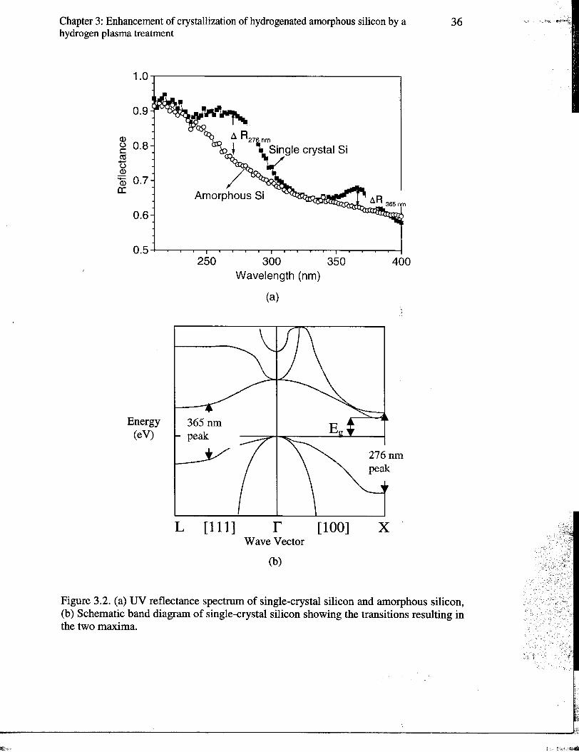
Chapter 3: Enhancement of crystallization of hydrogenated amorphous silicon by a 36 '" <"",c""~~~
hydrogen plasma treatment '
1.0
0.9 ~~~~
Q) ~ ~ R276 nm
g 0.8 (J!)(Q t -. Single crystal Si(Ij ,-u
~ 0.7 /a: Amorphous Si ~R
365 nm
0.6
0.5250 300 350 400
Wavelength (nm)
(a)
Energy(eV)
276 nm
pe.tk
L [111] r [100] XWave Vector
(b)
Figure 3.2. (a) UV reflectance spectrum of single-crystal silicon and amorphous silicon,(b) Schematic band diagram of single-crystal silicon showing the transitions resulting inthe two maxima.
""i"'!!".
Chapter 3: Enhancement of crystallization of hydrogenated amorphous silicon by a 37 ,...'
hydrogen plasma treatment
sample surface), R is the reflectance of the sample, and Ro is the reflectance of an
ideally smooth surface of the same material. The surface roughness of the a-Si:H film
after the hydrogen plasma treatment was -5 nm as determined from equation (3.1).
3.2.3. Other sample preparation and analysis techniques
Film thickness and optical constants by Swanepoel technique
Estimate of the thickness of the a-Si:H or polysilicon films can be obtained by
etching patterns in the film using a very selective (Si vs. SiO2) dry etch (SF6 plasma: RF
power 30 W, pressure 150 mtorr, flow rate 1.5 sccm), and then measuring the surface
profile with a Dektak Surface Profilometer. For accurate measurement of the thickness
of films deposited on glass substrates, the Swanepoel technique is used 29. It involves
measuring the optical transmission (A.: 300-2500 nm) of the film with a Hitachi H-3410
spectrophotometer, and determining the thickness of the film based on the interference
fringes of the transmission data (see Appendix B for details).
Infrared transmission measurement
To determine the net hydrogen content in the a-Si:H films and to determine the
type of hydrogen bonding in the films, the infrared transmission of the films was
measured. The infrared transmission of the samples with a-Si:H films deposited on bare
p-type lightly doped (-10-50 .Q-cm) Si wafers which were polished on both surfaces,
was measured on a Nicolet FTIR setup. Si wafers were used as substrates, as glass is not
transparent in the IR range. The net hydrogen content in atomic % in the a-Si:H films
can be then easily determined from the integrated absorption coefficient (a) at 630 cm-l
which arises due to wagging modes of Si-H and Si-H2 bonds 30 (See Appendix B for
details).
,,1 / y , f .'
,
~~.;"'

Chapter 3: Enhancement of crystallization of hydrogenated amorphous silicon by a 38hydrogen plasma treatment
TEM sample preparation
The sample preparation involved chemically etching a hole in the substrate to
realize an electron-transparent film (polysilicon layer) at the edge of the hole. First the
1.5-mm thick glass substrates or 500-!lm thick Si substrates were mechanically polished
to a thickness of -100 !lm. Then the sample was cleaved into small square pieces (2 mm
x 2 mm) with a blade. The small piece was mounted with silver paste face down, on a 3
mm diameter copper disc with a lattice of holes of -50 !lm in size. The sample was then
heated to 150 °c for 10 min to cure the silver paste. The Cu grid was then placed on a
teflon rod with the glass surface facing up. Molten beeswax was used to cover the
whole sample. A small hole was then punched through the soft wax using a pointed
stick to expose the glass. The rod, with the sample was immersed in an etchant.
The chemical etchant used was pure HF for glass substrates, and a mixture of
HF, HNO3 and CH3COOH for Si substrates. We had much better success with TEM
samples prepared in films deposited on glass substrates, as HF etches only the glass
substrate and does not etch the polysilicon film. On the other hand, the silicon etchant
also etches the oxide between the oxide and the substrate and then the polysilicon thin
film during the overetch time, hence damaging the film. Further work is needed to
prepare TEM samples in polysilicon films on SiOz/Si substrates using a dimpler and an
ion-milling machine to avoid etching of the polysilicon film, so that'grain size of
polysilicon films after a high-temperature anneal can be measured.
The etch rate of glass in HF is about 5 !lm/min. Etching is completed when the
glass is completely etched and polysilicon film is visible. As mentioned earlier HF
etches only glass and does not etch the polysilicon film, hence over etch can be
tolerated, though care has to be taken not to damage the polysilicon film. Finally the
.

Chapter 3: Enhancement of crystallization of hydrogenated amorphous silicon by a 39hydrogen plasma treatment
beeswax is removed by rinsing the sample in TCE at 60 °C 31. No ion milling was
required. The plan view transmission electron microscopy was done on a Philips CM
200 FEG-TEM with a 200 keY electron gun, courtesy of Nan Yao at the Princeton
Materials Institute.
3.3 CRYSTALLIZATION OF PLASMA-TREATED FILMS
3.3.1 Introduction
In our work, we studied the effect of hydrogen, oxygen and argon plasma
treatments before the thermal crystallization of a-Si:H (Fig. 3.3). In this example, the a-
Si:H film was 150 nm thick and deposited at 150 °C on Coming 7059 glass substrates.
The RF power was 200 W, pressure was 50 mtorr and flow rate 50 sccm. As discussed
in the previous section, the change in reflectance at 276 nm is used to monitor the
degree of crystallization. As can be seen in Fig. 3.3, crystallization of the a-Si:H films
as a function of annealing time, plasma-treated or untreated, involves two distinct
phases. During the first part, there is no crystallization and the UV reflectance peak at
276 nm is 0%, and this is the incubation period ('to). This is followed by the crystal
growth period ('tc), during which crystal growth occurs from the seed nuclei, and is
characterized by growth of the UV reflectance peak at 276 nm and its ultimate
saturation when the crystallization is complete. Fig. 3.3 also shows that the plasma
treatment reduces the incubation time with the crystal growth time being nearly
constant. A hydrogen plasma has the largest effect, with the total crystallization time,
defined as the time taken to completely crystallize a-Si:H film, at 600 °c in N2
ambient, reduced by a factor of five. Argon plasma had the smallest effect and oxygen
plasma resulted in reduction of crystallization time by about two.
~,-,,;"" ~",,#..~-.r~~

Chapter 3: Enhancement of crystallization of hydrogenated amorphous silicon by a 40hydrogen plasma treatment
8
7 polycrystalline
6
5-0~ 4 -,&- Exposed to H2 plasma
CI: -0-- Exposed to °2 plasma<] 3 -+- Exposed to Ar plasma
--0- Control, untreated sample2
1
0 ~~~~~J0 5 10 15 20 25
Annealing time at 600 DC (hrs)
Figure 3.3. Change in UV reflectance at 276 nm as a function of annealing time forsamples exposed to different plasmas at RF power of 200 W for 90 min.
In the subsequent sections, the effect of annealing temperature, the effects of RF
power and length of exposure, effect of growth temperature of the precursor film, the
effect of film thickness, and the effect of dopants in the film on the crystallization
behavior of untreated and hydrogen-plasma-treated films will be examined. The
material properties of the resulting polysilicon films and the masking effect of hard
masks like SiOz during the plasma treatment will also be discussed.
3.3.2 Effect of annealing temperature
The total crystallization time of 150 nm a-Si:H films deposited at 250 °c on
oxidized silicon substrates, either untreated or treated with hydrogen plasma at RF
power of 200 W for 90 min, and annealed at different temperatures, is plotted in Fig.
3.4. As is expected, both curves exhibit similar characteristics, and the total
crystallization time decreases as the annealing temperature is raised. A linear fit of the
data yields an apparent activation energy (EA) of 3.7 e V for the untreated control
-"'1'" ?""%,~

Chapter 3: Enhancement of crystallization of hydrogenated amorphous silicon by a 41hydrogen plasma treatment
Annealing temperature (oC)630 620 610 600 590 580 570 560
100 150 nm a-Si:H on SiOz/Sideposited at 250 °c
;§:Q)E
+"'
c.Q 10+"'Ct!
.!::!
"'ini;jC:"'()
"'in'0 1f- . Control sample, untreated
0 Hz plasma exposed (200 W, 90 min)
12.8 13.0 13.2 13.4 13.6 13.8
Reciprocal annealing temperature (1/kT) (eV.1)
Figure 3.4. Total crystallization time of a-Si:H films annealed as deposited or afterhydrogen plasma treatment, as function of annealing temperature.
sample, and 2.7 e V for the hydrogen-plasma-treated sample. These are not the actual
activation energy of a single process as the total crystallization time includes incubation
time and crystal growth time. The two processes of nucleation and crystal growth occur
at the same time once a few seeds have formed.
Separation of the crystallization time data of the various a-Si:H films into the
basic processes of nucleation (EA -5.0 e V) and crystal growth (EA -2.7 e V), is difficult
and requires grain size and nucleation density data for different anneal times 18, which
were not measured in this case. Not surprisingly, for the untreated control an EA
between the values of 2.7 eV and 5.0 eV is measured. In the hydrogen-plasma-treated
case, EA of 2.7 e V suggests fully created seeds, and that subsequent anneal leads to
growth. This is consistent with the near immediate rise in UV reflectance in Fig. 3.3.
.iill;\~"!"; !'f!'!';!'!'f;;,;r,=11~..1~';!'~~~A

Chapter 3: Enhancement of crystallization of hydrogenated amorphous silicon by a 42hydrogen plasma treatment
16 150 nm a-Si:H deposited on 7059
- 14 at 150 DC IIn...
J::-; 12 -0- H Plasma 90 minE 2 '";:; 10 -.-0 plasma, 90 minc:0
""E 8.~
~ 6 Sputter damage
~ "'!/0 4 /
20 50 100 150 200 250 300
RF Power (W)
(a)
16 150 nm a-Si:H deposited on 7059
- 14 at 150 DCIn...
J::'-' 12Q)
.§ -0- H2 plasma, 200 W";; 10 -.- 0 plasma, 200 W0
""E 8N
== --..s 6In
C:-
o 4 e
20 50 100 150 200
Plasma exposure time (min)
(b)
Figure 3.5. Crystallization time of a-Si:H plasma-treated samples as a function of (a)RF power and (b) exposure time, during exposure with chamber pressure of 50 mtorrand flow-rate of 50 sccm.
I
Chapter 3: Enhancement of crystallization of hydrogenated amorphous silicon by a 43
hydrogen plasma treatment
3.3.3 Effect of RF power and exposure time
The total crystallization time of the plasma-treated a-Si:H films on 7059 glass
substrates, falls as the RF power of the Hz or Oz plasma is increased as shown in Fig.
3.5(a). This indicates that the reduction in crystallization time of the films depends
strongly on the ion energy during the plasma exposure. In either case, when the RF
power density is greater than 1.08 W /cmz, the plasma exposure leads to sputter etching
of the film that produces pits and craters as observed by optical microscopy and Dektak
surface profile measurement. The total crystallization time also becomes shorter as the
plasma exposure time is increased and saturates after 60 min exposure in the case of Hz
and 180 min in the case of Oz plasma exposure, respectively, as illustrated in Fig.
3.5(b).
3.3.4 Effect of deposition temperature
The total crystallization time also depends on the growth temperature of the a-
Si:H films. The incubation time of crystallization of untreated samples increases as the
growth temperature is reduced with the characteristic crystallization time being nearly
constant. The total crystallization time falls linearly from -17 h to -5 h for the untreated
control sample as the growth temperature increases from 150 to 350 °c (Fig. 3.6(c».
This correlates well with the total hydrogen content (as measured by IR absorption at
630 cm-l) of the film, which also drops linearly from -16.9 to -8.5 at. % as the growth
temperature increases from 150 to 350 °c (Figs. 3.6(a) and 3.7(a». Also, as the
deposition temperature is lowered the IR absorption at 2000 cm-l corresponding to Si-H
bonds 32 remains fairly constant, while the IR absorption at 2090 cm-l by Si-Hz bonds 32
increases as can be seen in Figs. 3.6(b) and 3.7(b). Therefore the increase in hydrogen
content with decreasing growth temperature is predominantly due to the increase in
silicon-dihydridebonds 3°. The structural disorder in the film also increases with
'"

Chapter 3: Enhancement of crystallization of hydrogenated amorphous silicon by a 44hydrogen plasma treatment
(a)
18 a-Si:H on 7059 glass
16;:e:-o . 14
g"E 12Q)
§ 10uI 8
6100 150 200 250 300 350 400
Deposition Temperature (oC)
(b)0.020 . 0.005
- ' E. E - -:::::::::::=:- -.. 0 . 0 0 4 u
~ 0.015 8a .-a 0.003 C\JC\J -~ 0.010 ~~ 0.002 gc: <U<U .D.D 0.005 00 0.001 InIn .D.D «« 0.000 0.000
100 150 200 250 300 350 400
Deposition Temperature (oC)
(c)18
-8- no plasma treatment- 16 -A.-O2 plasma (200 W, 90 minI,[ 14 -e- H plasma (200 W, 90 minI
~ 12:;::.~ 10 k~ 8 .L~-"';"~
i 6 :=:::::::::::~ 4 :!: I--~==::==::;;()
2100 150 200 250 300 350 400
Deposition Temperature (oC)
Figure 3.6. (a) Hydrogen content in the a-Si:H film as a function of growth temperature,(b) IR absorbance at 2000 cm-l and at 2100 cm-l for a-Si:H films grown at differenttemperatures and, (c) Crystallization time for plasma-treated and untreated samples as afunction of growth temperature.
"'.c""""'r~~_~

Chapter 3: Enhancement of crystallization of hydrogenated amorphous silicon by a 45hydrogen plasma treatment
2500
- -a-Si:H at 150 °c- 2000 °";-E -0-- a-Si:H at 250 C
..s. - a-Si:H at 350 °c~ 1500-u~-Q)0u 1000c::0
-.;:;Co
g 500.Q<x:
0500 750 1000 1250 1500 1750 2000 2250
Wavenumber (cm-1)
(a)
75081-
a-Si:H at 150 °c .-'Eu- 500-c
"~"~'+-'+-Q)0u
§ 250"';::;Q.'-0cn
..a«01800 1900 2000 2100 2200
Wavenumber (cm-1)
(b)
Figure 3.7. Infrared absorption of a-Si:H films deposited on bare Si wafers at varioustemperatures. (a) Absorption coefficient at 630 and 2000 cm-l, with hydrogen contentdetermined from the 630 cm-l peak, and (b) absorption coefficient around 2000 cm-l,shows the increase in Si-H2 at lower growth temperatures.
~ - ~,-:

Chapter 3: Enhancement of crystallization of hydrogenated amorphous silicon by a 46 Ihydrogen plasma treatment
increasing hydrogen content in the film and increasing silicon-dihydride bonds. Others
have shown that, structural disorder in PECVD a-Si:H films, as measured by the Raman
intensity ratio of the longitudinal acoustic mode (320 cm-l) and the transverse optical
mode (480 cm-l), was found to increase as the growth temperature was reduced 33. The
more ordered arrangement of silicon tetrahedra, which are favorable sites for nucleation
for annealing, is possible at higher deposition temperatures, as the silicon species
(participating in growth of the film) have higher surface diffusivity 34. This increase in
structural disorder in amorphous fil~s deposited at lower temperature leads to slower
nucleation and therefore leads to increased incubation time during the crystallization
anneal. The effect of structural disorder in the precursor a-Si:H films on the,
crystallization kinetics will be discussed in further detail in Section 6.2.1. The total
crystallization time of oxygen-plasma-treated samples (Fig. 3.6(c» also drops as the
deposition temperature increases, as does the crystallization time of the control samples.
But the hydrogen-plasma-treated samples show no important change in total
crystallization time with growth temperature (Fig. 3.6(c», and in fact the total
crystallization time increases slightly from -4 h to -5 h when the deposition
temperature is raised from 150 to 250 °C, unlike the control samples.
From this we infer that the number of incipient nucleation sites in untreated or
oxygen-plasma-treated films is increased as the PECVD growth temperature is raised.
The relative constancy of the total crystallization time of the hydrogen-plasma-treated
sample irrespective of the growth conditions suggests that, the seeding layer produced
by the plasma treatment is the same regardless of starting conditions. The effect of
deposition temperature on the crystallization time of the hydrogen-plasma-treated films
will be discussed in detail in Section 3.4.3.
""""

Chapter 3: Enhancement of crystallization of hydrogenated amorphous silicon by a 47 'Ihydrogen plasma treatment,
20 ~ ~ a-Si:H deposited at 150 DC
~ Annealed at 600 DC
;s:EQ) 1 5 a--- -.-.;:;
I::0
-.;:;ro~ 10 . untreated control"* 0 H2 plasma treatedC:-o
5 a-_~~:e: ~
0100 200 300 400 500 600
Precursor a-Si:H thickness (nm)
Figure 3.8. Crystallization time of a-Si:H films, both untreated and hydrogen-plasma-treated, deposited at 150 °c on Coming 7059 pre-annealed glass substrates, as afunction of film thickness. Data shows the drop of crystallization time on the filmthickness for the untreated case.
3.3.5 Effect of film thickness
The crystallization time of untreated a-Si:H films also depends on the thickness
of the films, with thinner films taking longer time to crystallize. The crystallization time
remained constant when the film thickness was above -300 nm (Fig. 3.8). This
dependence was seen for films deposited at either 150 °c or 250 °c on 7059 glass
substrates. The crystallization time of the hydrogen-plasma-treated samples, however,
did not show such a strong dependence on the film thickness. This effect of film
thickness on the crystallization time of the amorphous films might be due to the in-built
stress concentrated at the a-Si:Wsubstrate interface, which if tensile might inhibit
nucleation during the anneal 35-37, as tensile stress makes it difficult for the silicon
atoms to come together and bond with each other (necessary to form seed crystallites).
Earlier work has shown that a-Si:H films deposited at 230 °c by RF PECVD on 7059
.
r '"I
""c1--'c~
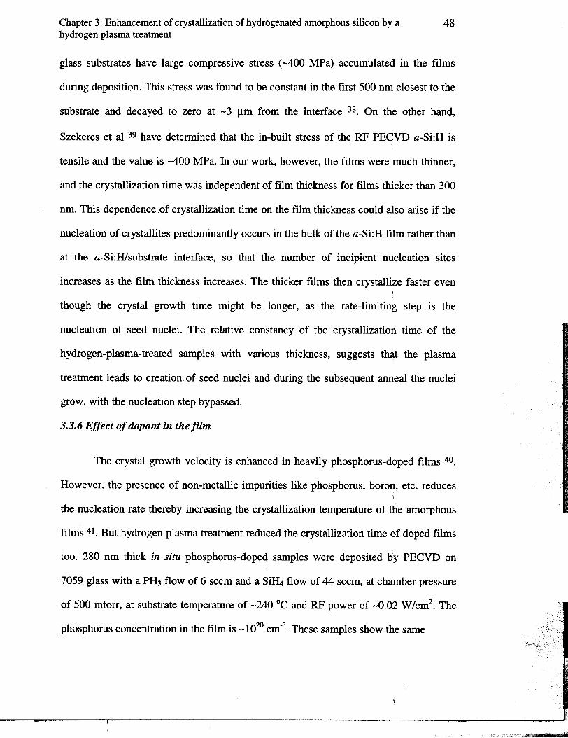
Chapter 3: Enhancement of crystallization of hydrogenated amorphous silicon by a 48hydrogen plasma treatment
glass substrates have large compressive stress (-400 MPa) accumulated in the films
during deposition. This stress was found to be constant in the first 500 nm closest to the
substrate and decayed to zero at -3 ~m from the interface 38. On the other hand,
Szekeres et al 39 have determined that the in-built stress of the RF PECVD a-Si:H is
tensile and the value is -400 MPa. In our work, however, the films were much thinner,
and the crystallization time was independent of film thickness for films thicker than 300
nm. This dependence of crystallization time on the film thickness could also arise if the
nucleation of crystallites predominantly occurs in the bulk of the a-Si:H film rather than
at the a-Si:H/substrate interface, so that the number of incipient nucleation sites
increases as the film thickness increases. The thicker films then crystallize faster even
though the crystal growth time might be longer, as the rate-limiting step is the
nucleation of seed nuclei. The relative constancy of the crystallization time of the
hydrogen-plasma-treated samples with various thickness, suggests that the plasma
treatment leads to creation of seed nuclei and during the subsequent anneal the nuclei
grow, with the nucleation step bypassed.
3.3.6 Effect of dopant in the film
The crystal growth velocity is enhanced in heavily phosphorus-doped films 4°.
However, the presence of non-metallic impurities like phosphorus, boron, etc. reduces
the nucleation rate thereby increasing the crystallization temperature of the amorphous
films 41. But hydrogen plasma treatment reduced the crystallization time of doped films
too. 280 nm thick in situ phosphorus-doped samples were deposited by PECVD on
7059 glass with a PH3 flow of 6 sccm and a SiH4 flow of 44 sccm, at chamber pressure
of 500 mtorr, at substrate temperature of -240 °c and RF power of -0.02 W/cm2. The
phosphorus concentration in the film is -1020 cm-3. These samples show the same
fc"+""CCC'~~

Chapter 3: Enhancement of crystallization of hydrogenated amorphous silicon by a 49hydrogen plasma treatment
280 nm n-a:Si-H @ 240°Cannealed at 600 °c 8
107 ..A..,""'. c c .~ f c.."Q
. .: ", 6- '
- 'Q) :
~ 105 ::J ' -co 4 ~(/) ment ~a a:- '<Jw "
~ 103 ",
c: ", 2
Co
'c c
101 00 5 10 15 20 25
Anneal time at 600°C (hrs)
Figure 3,9, Dopant activation and UV reflectance during annealing of a hydrogen-plasma-treated, and an untreated a-Si:H film doped with phosphorus at -1020 cm-3 andgrown at -240°C on glass,
crystallization trend as the intrinsic a-Si:H films with the hydr?gen plasma treatment
reducing the crystallization time from -24 to <4 h (Fig, 3.9). In fact the crystallization
time is slightly smaller than that for the undoped hydrogen-plasma-treated sample due
to the enhanced crystal growth velocity of phosphorus doped films, The ultimate sheet
resistance (-25 Wsquare) after annealing at 600 °c in N2 of the H2-plasma-treated
sample is the same as the untreated control sample,
3.3.7 Selective Crystallization
Selective crystallization can be accomplished by using a patterned hard mask
like SiO2 or SiNx during the plasma treatment and subsequent anneal of the sample 13,
14, To demonstrate selective crystallization, -100 nm of silicon dioxide (SiOv was
deposited bye-beam evaporation on top of 150 nm of a-Si:H film deposited at 150 °C.
The SiO2 was then patterned and the samples were exposed to hydrogen plasma. Then
!;'Ii
_t.i.
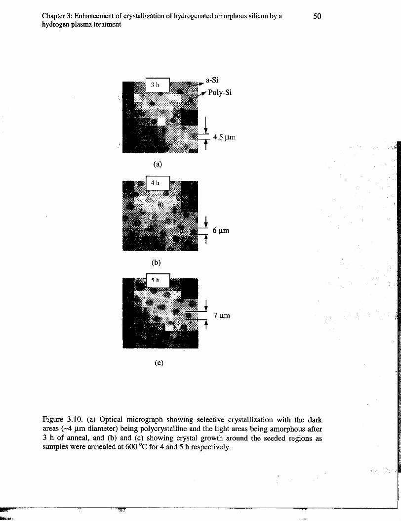
Chapter 3: Enhancement of crystallization of hydrogenated amorphous silicon by a 50hydrogen plasma treatment
Si
Poly-Si
4.5~m
(a)
6~m
(b)
7~m
(c)
Figure 3.10. (a) Optical micrograph showing selective crystallization with the darkareas (-4 ~m diameter) being polycrystalline and the light areas being amorphous after3 h of anneal, and (b) and (c) showing crystal growth around the seeded regions assamples were annealed at 600 °c for 4 and 5 h respectively.
~"

Chapter 3: Enhancement of crystallization of hydrogenated amorphous silicon by a 51hydrogen plasma treatment
all the remaining SiO2 was stripped and the samples were annealed in the furnace. The
exposed areas crystallized completely as expected, while the unexposed areas remain
amorphous as can be seen in Fig. 3.10(a), and this was also confirmed by UV
reflectance measurements. This shows that SiO2 can mask against the effect of the
plasma. Lateral crystallization does occur, however, with the crystal front growing out
of the seeded (exposed) areas to the unexposed areas as can be seen in Figs. 3.10(b) and
3.10(c) and in Fig. 3.12(b) with the lateral growth rate being -0.5 ~m/h at 600 °c. This
is one of the most important advantages of the plasma-enhancement effect and its use in
fabricating better performance polysilicon TFTs and in integrating a-Si:H and poly-Si
TFTs on the same substrate will be discussed in detail in chapters 4 and 5, respectively.
Other hard masks and their effect on crystallization of a-Si:H
When -100 nm thick SiO2 deposited on the a-Si:H film by PECVD at 280 °c'-
with N2G flow of 475 sccm and Si~ flow of 200 sccm, pressure of 900 mtorr and RF
power density of -0.08 W /cm2, was used to mask the effect of plasma, it led to
significant peeling of the film. Subsequent anneal of the samples after the oxide was
stripped showed that crystallization time of the a-Si:H with prior oxide deposition was
lower compared to the film with no oxide deposition step. In addition, it was found that
the SiO2 layer was quite porous and did not effectively mask the effect of the plasma.
The peeling of the film was eliminated, and the reduction in the crystallization time due
the oxide deposition step was minimizeC\ by changing the growth temperature of the
SiO2 to 250 °c and using lower flow rates of SiH4 (35 sccm) and N2O (160 sccm).
However, -100 nm of SiO2 deposited by electron beam evaporation was found to the
least intrusive with no change in the crystallization time of the a-Si:H films due to the
SiO2 deposition step, and also effectively masked the effect of the plasma as discussed
above. SiNx deposited by PECVD was also tried as a hard mask. As in the case of the

Chapter 3: Enhancement of crystallization of hydrogenated amorphous silicon by a 52hydrogen plasma treatment
SiOz, high-temperature (-300 °C) growth led to significant reduction in the
crystallization time of the a-Si:H films. The growth temperature was ther.efore lowered
to -200 °c and hydrogen dilution was added to the plasma to improve the structural
rigidity of the SiNx layer 42. In this case the SiNx, which is a good diffusion barrier, was
left on during the anneal to minimize the hydrogen effusion from the a-Si:H regions
during the high-temperature crystallization anneal. This helps somewhat to preserve the
quality of the amorphous regions (discussed in Section 5.3). The gate oxide/n+ a-Si:H
stack was also used successfully to mask the plasma effect (Section 4.5).
3.3.8 Material characteristics of the films
The grains of completely crystallized (annealing at 600 °C) either 300 or 150 nm
thick a-Si:H films deposited at 150,250 or 350 °c, were predominantly oriented in the
[111] vertical direction (Fig. 3.11) regardless of plasma treatment prior to SPC. Other
work has shown that grains with (111) oriented surfaces predominate as the (111) plane
has the least surface energy 43. It was also speculated that in SPC (111) planes for
energetic reasons bound the initial critical crystalline clusters (nuclei) which initiate
growth. This results in the grains with (111) orientation and also results in twinning
defects within the grain 44. Others have speculated that the (Ill) texture (vertical) of the I
SPC films is due to the different growth rates of the crystalline fronts with differentI
orientation, and surface oriented in [111] vertical direction has the slowest growth rate
45. We will discuss this in more detail later in Section 6.5.I
In very thin films «100 nm), the interface energy at the top or bottom of the
film can also provide significant driving force for grain-size enhancement termed as
secondary grain growth, so that grains substantially larger than the film thickness can be
obtained. {Ill} -oriented grains are often found after this secondary recrystallization
7- ,.~c~ - I; "",1.,1'fl"",

Chapter 3: Enhancement of crystallization of hydrogenated amorphous silicon by a 53hydrogen plasma treatment
(111)
Contrd Sarrple, untreated
I (220)
-- ~~~~~~-U)
."!::c::J
..cI-Ctj
-;: I-tydrogen pasrm exposed-'wc:
.~ ...,. ..., ...,~, ~
>- 1'-,y~~~~~~~IiI"~ ~Ctjl-I
><
Oxygen pasrm exposed
I,~.,,-~~ 'I
;~~
20 30 40 &) 00 70
Dffroction argle 28 (deg)
Figure 3.11. X-ray diffraction of completely crystallized samples, as deposited or withprior hydrogen or oxygen plasma treatment, showing that the grains are predominantlyoriented in the (111) direction.
of a bare polysilicon surface because the energy of a free silicon surface with this
orientation is minimum 43,
On the other hand, the interface energy of an Si/SiOz interface favors formation
of {100}-oriented grains 43, In the case of direct deposition of polysilicon films by
various CVD techniques, the <110> orientation is widely seen, though other
orientations are found depending on the groVith conditions 46, In the case of low-
pressure CVD using silane for example, the <110> orientation occurs mainly around a
,) I
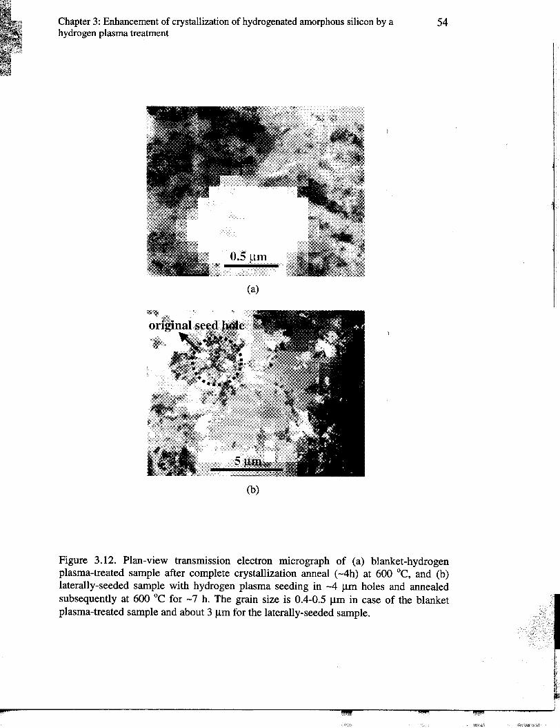
Chapter 3: Enhancement of crystallization of hydrogenated amorphous silicon by a 54hydrogen plasma treatment
I"Q"
,
(a)
(b)
Figure 3.12. Plan-view transmission electron micrograph of (a) blanket-hydrogenplasma-treated sample after complete crystallization anneal (-4h) at 600 °c, and (b)laterally-seeded sample with hydrogen plasma seeding in -4 !lm holes and annealedsubsequently at 600 °c for -7 h. The grain size is 0.4-0.5 !lm in case of the blanketplasma-treated sample and about 3 !lm for the laterally-seeded sample.

Chapter 3: Enhancement of crystallization of hydrogenated amorphous silicon by a 55hydrogen plasma treatment
temperature of 625 °c, while the <100> and <Ill> orientation occur at higher
temperatures than about 650 °C 47. The <110> orientation occurs due to the higher
growth rate in that direction, which is twice that of in the <111> direction, is explained
by the difference in surface energy by some 48. We will discuss the factors determining
grain orientation in SPC films and methods to control it further in Section 6.5.
The grain size of the 150 nm thick polysilicon film as measured by TEM
annealed without plasma treatment was -0.6 ~m, while the plasma-treated and annealed
samples had grains of about 0.4 - 0.5 ~m (Fig. 3.12(a)). The grains show the well-
known highly twinned structure of SPC films 44. In both cases, the grain size was
substantially larger than the film thickness, unlike the as-deposited polysilicon with
much smaller grains. Selective area diffraction of the films during TEM also confirmed
that most of the grains had (111) vertical orientation, consistent with the XRD results.
Fig. 3.12 (b) shows the lateral grain growth from the hydrogen plasma-seeded regions,
with larger grains (up to 3 ~m) in the lateral growth region. This illustrates how the
plasma-enhancement effect can be used to engineer larger grains in specified regions. In
Section 4.5 we will discuss the use of this technique to enhance transistor performance.
3.4 MECHANISM OF SEEDING BY HYDROGEN PLASMA
In this section we propose a model to explain the hydrogen plasma enhancement
of crystallization of the a-Si:H films. The main idea is that the fairly high energy
hydrogen ions in the hydrogen plasma bombard the surface (up to a few hundred
angstroms below the surface) of a-Si:H film and insert themselves in Si-H bonds and
abstract hydrogen from the unit leading to Si dangling bonds. The formation of the Si
dangling bonds promotes the formation of Si-Si bonds, which leads to growth of silicon
crystalline clusters. During the subsequent crystallization anneal, these clusters grow
"""'~ ~~ J

Chapter 3: Enhancement of crystallization of hydrogenated amorphous silicon by a 56hydrogen plasma treatment
thereby enhancing the crystallization process. This model is controversial, as there is
only indirect evidence of such crystallite formation due to hydrogen plasma exposure.
Typical hydrogen-plasma-induced crystallinity was directly observed only during the
growth of micro/poly-crystalline silicon using layer-by-layer growth 49, 50 or high
hydrogen dilution during growth 51.
3.4.1 Location of seed nuclei
In the preceding section we suggested that the hydrogen plasma created seed
nuclei which resulted in reducing the total crystallization time. In this section we
determine the location of the seed layer and its composition. To test if the effect of the
hydrogen plasma treatment on the crystallization occurred through a modification of
only the surface of the amorphous silicon film, we dry-etched the hydrogen-plasma-
treated sample to various depths in an SF6 plasma in Plasma TechnologyRIE chamber
(RF power of 10 W, SF6 flow rate of 15 sccm and chamber pressure of 150 mtorr)
before annealing. The resulting thickness of the films was measured by the Swanepoel
technique 29 from the optical transmission data, for accuracy (see Appendix B for
details).
We then observed the effect of such etching on the crystallization time. To
ensure that the SF6 plasma itself did not affect the crystallization times, control a-Si:H
samples unexposed to any H2 plasma are etched simultaneously and the crystallization
times of these samples were also measured. All these control samples had the same
crystallization time of -15 h, irrespective of the thickness of a-Si:H etched in the SF6
plasma, hence demonstrating that the dry-etch process itself does not affect the
crystallization time. As can be seen in Fig. 3.13(a), a hydrogen-plasma-treated sample
with the top -40 nm thick layer removed crystallizes in the same time as an untreated
sample. This proves that the surface region is responsible for rapid crystallization and
~ii'

Chapter 3: Enhancement of crystallization of hydrogenated amorphous silicon by a 57hydrogen plasma treatment
(a)18
15 -I-I- \:~ +6- 12 Crystallization time~ of untreated sample:;::;c 90
:;::;c13N
== 6c13
~ 150 nm a-Si:H deposited at 150 DC() 3 H2 plasma,200 W, 90 min
0 10 20 30 40 50 60 70
Etched depth (nm)
(b)";-E 0.21 18u .gO. 1 8 ,,~~~;;:£--t--"£ i 1 6 (\j 14 ~
- .cc13 0.15 12 -;§ Crystallization time E.- :;::;0.. 0.12 10 c'- 00 .-.2 0.09 H2 plasma 8 m
~ 200 W, 90 min 6 ~Q) " '~::~=-~ 0.06 4 ~c13 ()E'6 0.03 2z ,
0 10 20 30 40 50 60 70 IDepth from surface (nm) I
Figure 3.13. (a) Crystallization time of samples etched to different depths by SF6plasma (20 W, 150 mtorr, and 15 sccm) after hydrogen plasma treatment at 200W for90 min, and (b) IR absorption at 2100 cm-l as function of depth from the surface for thissample.
i
,+~"';
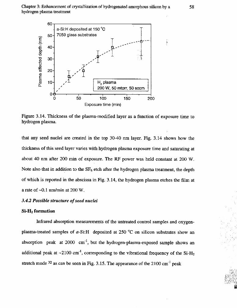
Chapter 3: Enhancement of crystallization of hydrogenated amorphous silicon by a 58hydrogen plasma treatment
60a-Si:H deposited at 150 DC
T- 50 7059 glass substratesE f -1 ; ,s ~~~-- IjJ \'
:5 40 ,,~~- !Co f '~ iQ) .."
-c ....-c 30 .." "~Q) ..
+"' ..Co) ,Q) f~ 20 " !f ' ro 'E .-
~ 10.-'- H2 plasma0-.-'- 200 W, 50 mtorr, 50 sccm i.-
00 50 100 150 200
Exposure time (min) I
Figure 3.14. Thickness of the plasma-modified layer as a function of exposure time tohydrogen plasma.
that any seed nuclei are created in the top 30-40 nm layer. Fig. 3.14 shows how the
thickness of this seed layer varies with hydrogen plasma exposure time and saturating at
about 40 nm after 200 min of exposure. The RF power was held constant at 200 W.
Note also that in addition to the SF6 etch after the hydrogen plasma treatment, the depth
of which is reported in the abscissa in Fig. 3.14, the hydrogen plasma etches the film at
a rate of -0.1 nm/min at 200 W.
3.4.2 Possible structure of seed nuclei
Si-H2 formation
Infrared absorption measurements of the untreated control samples and oxygen-
plasma-treated samples of a-Si:H deposited at 250 °c on silicon substrates show an
absorption peak at 2000 cm-l, but the hydrogen-plasma-exposed sample shows an
additional peak at -2100 cm-l, corresponding to the vibrational frequency of the Si-H2
stretch mode 32 as can be seen in Fig. 3.15. The appearance of the 2100 cm-l peak
c~ !

Chapter 3: Enhancement of crystallization of hydrogenated amorphous silicon by a 59hydrogen plasma treatment
0.020
Si-H vibrational freq-1at 2000 cm
0,015
Q)Co)c:co 0.01 0 ~ S ' H ' b t.
I-e / ~ 1- 2 VI ra lonac9; Control ~ freq at 2100 cm-1~ untreated . ,
0,005 .J~,
to;
0.0001 1950 2000 2050 0
Wavenumber (cm-1)
Figure 3.15. The infrared spectra of a-Si:H films deposited at 250 °c, as deposited orhydrogen or oxygen plasma-treated. The hydrogen-plasma-treated sample shows ashoulder at 2100 cm-l corresponding to Si-H2 stretching mode and the 2000 cm-l peakcorresponding to Si-H bonds reduces slightly. This is made clearer in Fig. 3.16.
shows that the hydrogen plasma treatment changes the microstructure of the a-Si:H
film, producing Si-H2 bonds. On the other hand, the oxygen-plasma-treated samples
show no such shoulder formation and the infrared absorbance is similar to that of the
control untreated samples. We will discuss the effect of oxygen plasma treatment on the
a-Si:H film in further detail later in Section 3.5. Fig. 3.16 shows the integrated
absorption at 2000 cm-l and 2100 cm-l as a function of the hydrogen exposure time,
with the 2100 cm-l absorption increasing with hydrogen plasma exposure, indicating an
increase in hydrogen bonded as Si-H2. This effect, however, saturates after -60 min of
hydrogen plasma exposure. On the other hand the absorption at 2000 cm-l decreases
with hydrogen plasma treatment indicating a decrease in hydrogen bonded as Si-H with
hydrogen plasma exposure. The net hydrogen content in the film, calculated from
~"., i
~'fC

Chapter 3: Enhancement of crystallization of hydrogenated amorphous silicon by a 60hydrogen plasma treatment
90002~ 58000 H2 plasma at 0.8 W/cm --:-
~ ---,-~~ ,~~~~~ o 8000 ~
';-E 57500 -;;-
u 0
0 0 ,". 7000 ..-
0 57000 C\J0 -C\J (tj
"'in 56500 6000 §c ~
0 e-~ 56000 5000 g0 .c(/) (tj
.c "0~ 55500 : :::-;;;~ 4000 2-
Q) ~1§ 55000 g>'2 300 nm a-Si:H deposited on Si wafe . 3000 EE:. 54500 at 250 °c
2000
0 20 40 60 80 100 120 140 160
Exposure time (min)
Figure 3.16. Integrated absorption at 2000 cm-I and 2100 cm-I as a function of the
hydrogen exposure time of a-Si:H samples deposited on bare Si substrates. Clear
evidence of formation of Si-H2 after hydrogen plasma treatment.
integrated absorption at 630 cm-I dropped slightly from -10.5 at. % to -9.6 at. % after
150 min of hydrogen plasma treatment. As the samples were progressively etched in the
SF6 plasma to increasing depths, the absorption peak at 2100 cm-I, as described in the
previous section was reduced correspondingly. Fig. 3.l3(b) shows that this observation
correlates well with the increase of the total crystallization time.
Hydrogen depletion at surface
The hydrogen plasma treatment leads to formation of Si-H2 at the surface and
the net hydrogen content, as measured by the net IR absorption, in the film drops.
Secondary ion mass spectroscopy (SIMS) analysis of the films corroborated these
::0. ::::::o::~: i:::: t:l=a::::;F:~:~:: (a :~::::: ~::e:se t~~,J1
~!iJ'
_'
I
IJ

Chapter 3: Enhancement of crystallization of hydrogenated amorphous silicon by a 61hydrogen plasma treatment
(a)
1023 0a-Si:H as-deposited at 150 C
- ~ on 7059 glassM 22
.Q 1 0 . <:f' 0. ,~ ~...a.~~~-:e:--6;~~H i n f i I m
U) ~-.. - oQo 0- - -~.-E' "0-'0 1021 . rj' "- . }.~ . "(
~ 20 q:~~:=::;;> After H2 plasma exposure~ 10 "Q at 200 W for 90 min'- ,- Ic ~ . ,Q) 1019 .0.U "0-C00 18
10 0 20 40 60
Depth from surface (nm)
(b)2310 as-is a-Si:H deposited at 2500 C
- i on 7059 glassM 22
E 10 Q . .U 0- 0" , 0. ~ ~ H In fllm~- ~ ~ ~ oQo .a. -0- -0. ~U)' '0- ~ "D-E --- :;";~"-!W:-:Q:0 1 021 : '.,:§. (::;:=~ After H2 plasma exposurec .'.2 1020 Q, at 200 W for 90 min- .~ Q-E '0. 0 in filmQ) 1 19 ~~c~a . ": 8- .U 0 - v-u-o-~o.O-O-o.O-o.6-
c0
01018
0 20 40 60
Depth from surface (nm)
Figure 3.17. (a) Hydrogen and oxygen concentration ofa-Si:H films deposited at lSO°Cbefore and after hydrogen plasma exposure, showing hydrogen depletion from thesurface of the film, and (b) the same for film grown at 2S0°C, showing less hydrogendepletion. The reduction of hydrogen concentration at the surface is a fairly reliableindicator of conversion from a-Si:H to micro or nano-crystalline silicon,

Chapter 3: Enhancement of crystallization of hydrogenated amorphous silicon by a 62 I
hydrogen plasma treatment
agrees well with the seed nuclei layer thickness as detemlined by progressive etching of
the film, which we just discussed. The hydrogen depletion effect is not as pronounced in
a-Si:H films deposited at higher temperatures (Fig. 3.17(b». After a hydrogen plasma
treatment at RF power of 200 W for 90 min the surface hydrogen concentration
increased from 1x1019 cm-3 to 8x1019 cm-3 for films whose growth temperature
increased from 150 to 250 °C. This depletion effect is consistent with earlier infrared
absorption measurement as the IR data measures the total hydrogen concentration in the
fi1fi) while SIMS measures the hydrogen concentration throughout the film. It is
interesting to note that, even though the hydrogen concentration at the surface of the j
film is reduced to -1020 cm-3 after the hydrogen plasma treatment, the integrated
infrared absorption at 2100 cm-l increases by nearly four after the plasma treatment
(Fig. 3.16). This illustrates the sensitivity of the infrared measurement to changes in the
hydrogen-bonding configuration even in thin layers of the a-Si:H film.
In addition to hydrogen depletion, the hydrogen plasma treatment also leads to
an increase in oxygen concentration at the surface of the a-Si:H as seen in Fig.3.17(a).
The anomalously high oxygen levels at the surface might be due to SIMS artifact, as the
samples had a thin native oxide at the surface and the sputter etching of the film during
the SIMS measurement resulted in the oxygen at the surface being pushed in deeper into
the sample.
Aluminum sputter effect
High metal contamination levels are also known to lead to an increased
crystallization rate of amorphous silicon 2, 52. SIMS showed that the plasma treatment
produced aluminum contamination (Fig. 3.18), whose source is the aluminum oxide
electrode plate that is getting sputtered onto the sample. (The -4 cm2 samples were
placed directly on an aluminum oxide coated electrode.) It is thought, however, that the
~ I! I

Chapter 3: Enhancement of crystallization of hydrogenated amorphous silicon by a 63hydrogen plasma treatment
1 E19 ~~ After H2 plasma treatment,T V ~~ ~ vY sample placed directly on AI electrode- 1E18
'?E(.)
~ 1E17
~ ~/\-~..- '-y~"T-'? ~+-' 1 E16 ~~ y?-"--?c:Q) Control sample, not exposed(.)c: to plasma0 1 E15 ~ ~0 Sample placed on:;:( a Si wafer during --- -'" ~ -A-..
1 E14 H2 plasma exposure v.Av---~ I
0 20 40 60 80 100
Depth (nm)
Figure 3.18. Aluminum concentration at the surface of the a-Si:H films after H2 plasmaexposure with sample placed directly on the electrode vs. on a Si wafer.
concentration of aluminum (-5x1018 cm-3) at the surface of the sample is insufficient to
cause any significant change in crystallization times 52. Typically the crystallization
temperature for Al-Si alloys drops significantly for Al concentration of 4 at. % or
higher. This was confirmed by placing the a-Si:H samples on a 100 mm silicon wafer
(itself placed on the Al2O3 electrode) during exposure to plasma. This reduced the
aluminum contamination to below 1017 cm-3, which is the same as the untreated sample
(Fig. 3.18), so we conclude that the electrode was the source of the aluminum
contamination. These samples crystallized within the same time as the sample that was
placed directly on the aluminum electrode, so aluminum contamination is not
responsible for the enhanced crystallization effect.

Chapter 3: Enhancement of crystallization of hydrogenated amorphous silicon by' a 64hydr.ogen plasma treatment
3.4.3 Discussion
Weare not aware of any work showing similar hydrogen depletion at the surface
of ~-Si:H film by a hydrogen plasma treatment in another chamber after growth.
However, there has been a series of work involving so-called chemical annealing in the
PECVD growth chamber, whereby a thin a-Si:H layer is exposed to a hydrogen plasma
or hydrogen radicals after the growth of the thin layer 53. This has been shown to cause
depletion of hydrogen from the surface of a-Si:H film. Exposure of a-Si:H films to
atomic hydrogen during a hydrogen plasma treatment leads to hydrogen abstraction
from SiR or SiH2units, hydrogen insertion and/or etching of the film. The reactions are
54.
(a) Hydrogen abstraction from SiR unit:
(Si)3 - Si - H + H ~ (Si)3 - Si e+Hz(g), (3.2)
(b) Hydrogen abstraction from SiH2 unit::1
(Si)z - Si- H + H ~ (Si)z - Sie +Hz(g), (3.3)I I
H H
(c) Etching through multiple hydrogen insertion:
(Si)3 - Si - H + H ~ (Si)z - Si -Hz + Sie, (3.4)
(Si)z - Si - Hz + H ~ (Si) - Si - H3 + Sie, (3.5)
(Si)3 - Si- Si - H3 + H ~ (Si)3 - Si e+SiH4(g), (3.6)
(Si)3 - Si - Si -H3 + SiH3 ~ (Si)3 - Si e+SizH6(g), (3.7)
Of these reactions, abstraction reaction (3.2) and (3.3), insertion reactions (3.4), (3.5)
and (3.6) might occur in our experiments of exposure of a-Si:H films to atomic
hydrogen. The etch reaction (3.7) is expected to be more important during the
deposition of a-Si:H where SiR3 radicals are predominant 54. The energy of the
- ! J

Chapter 3: Enhancement of crystallization of hydrogenated amorphous silicon by a 65hydrogen plasma treatment
hydrogen ions during the plasma treatment would also determine which reaction among
(3.2) to (3.3) would be dominant. In our work, the DC self-bias during the hydrogen
plasma treatment was -500 V (as measured by the voltmeter on the Plasma Therm RIB
system), indicating that the ion energies are -500 eV. The SIMS data discussed in
Section 3.4.2 shows that hydrogen plasma treatment leads to substantial hydrogen
depletion from the surface of the film. This indicates that hydrogen abstraction reactions
(3.2) and (3.3) are dominant during the typical hydrogen plasma treatment. When the !
hydrogen plasma power was increased above 1.08 W/cmz or -600 V DC self-bias, the
etching reactions (3.4), (3.5) and (3.6) were dominant leading to considerable etching of
the film.
Hydrogen abstraction is thought to lead to the formation of crystallites in the,
layer-by-layer growth of microcrystalline silicon (J,lc-Si:H), which involves alternating a
Si~ plasma to deposit the a-Si:H film with a pure Hz plasma to create microcrystallites
of silicon in the surface layer 49, 50, 54. As can be seen from reaction (3.2) and (3.3),
hydrogen abstraction leads to the formation of silicon dangling bonds. This promotes
crystallization where two adjacent silicon dangling bonds join to form crystal-like bond.
Similarly, the growth of J,lc-Si:H by hydrogen dilution involves adding Hz to Si~
during growth and here the hydrogen abstraction occurs during the growth phase itself
and promotes crystallinity in the film 51. The hydrogen depletion will be more efficient
if the silicon dihydride content in the film is higher, and in fact the formation of a
porous SiHn phase is an important step towards hydrogen induced crystallization 5°. As
mentioned earlier, the films deposited at low temperatures (150 °C) have a higher
dihydride content than films deposited at 250 °c, leading to higher hydrogen depletion
from the surface of low-temperature films (Figs. 3.17(a) and (b». This could in turn
lead to a higher number of seed nuclei which explains why the crystallization time
i~ ,"' _wr'

Chapter 3: Enhancement of crystallization of hydrogenated amorphous silicon by a 66hydrogen plasma treatment
decreased from -5 h to -4 h for the hydrogen-plasma-treated samples when the growth;,
temperature was lowered from 250 °C to 150 °C.
The infrared absorption spectra of Jlc-Si:H films also show a peak at 2100 cm-l
55, because Si-H2 bonds predominantly terminate the microcrystallites of silicon
embedded in an amorphous matrix 54,55. This could explain why the hydrogen plasma
treatment of the a-Si:H film results in a peak at 2100 cm-l, and why this microstructural
change is limited to the top surface layer of the a-Si:H film. Figs. 3.17 (a) and (b) show
that the concentration of hydrogen at the surface of the a-Si:H film after the hydrogen
plasma treatment is very low, suggesting that the top layer is nearly pure silicon in the
form of a layer of silicon microcrystallites. The high concentration of oxygen in the
films could be from post H2 plasma exposure to oxygen in the atmosphere, because
hydrogen removal from the surface makes it extremely reactive and oxygen passivates
the dangling bonds at the surface 56. The enhancement of crystallization is not due to
the high oxygen concentration as it is known that oxygen inhibits crystallization 57. The
high oxygen levels at the surface could be a SIMS artifact due to a surface oxide as
discussed in Section 3.4.2. This native oxide can be etched by rinsing the film in dilute
HF before transistor fabrication.
The infrared absorption spectra, the crystallization time data, and the SIMS
analysis of our samples are consistent with the fact that the hydrogen plasma treatment
leads to the creation of small amounts of microcrystallites of silicon in the surface layer,
which could then act as seeds during the subsequent crystallization process. While we
have these indirect proofs for such an effect, we do not have direct evidence of the
formation of microcrystallites of silicon such as Raman spectra with a peak at 522 cm-l,
or lattice plane imaging with high resolution TEM (HRTEM). This might be because
the number and size of crystallites formed after the plasma treatment is too small to be
",
,I
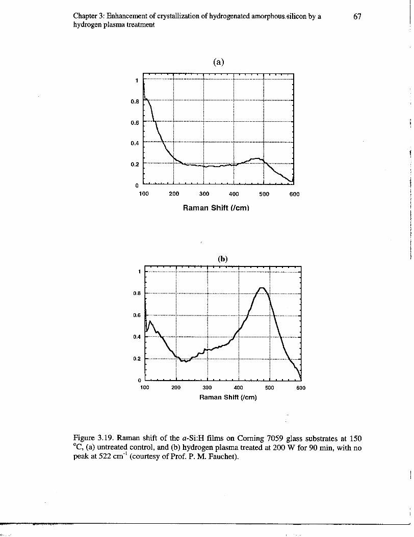
Chapter 3: Enhancement of crystallization of hydrogenated amorphous, silicon by a 67hydrogen plasma treatment
(a)
1
0.8
:::
0.2 + t.
0
100 200 300 400 500 600
Raman Shift (/cm)
(b)1
0.8
0.6
0.4
0.2
0100 200 300 400 500 600
Raman Shift (/cm)
Figure 3.19. Raman shift of the a-Si:H films on Corning 7059 glass substrates at 150°c, (a) untreated control, and (b) hydrogen plasma treated at 200 W for 90 min, with nopeak at 522 cm-l (courtesy of Prof. P. M. Fauchet).
i
~ ,""c.cc""c '

Chapter 3: Enhancement of crystallization of hydrogenated amorphous silicon by a 68hydrogen plasma treatment
detected by these methods. We measured the Raman spectrum for these samples in
collaboration with Prof. P. M. Fauchet of University of Rochester. The Raman spectrum;'
of the untreated and hydrogen-plasma-treated samples is shown in Fig: 3.19, which
indicates that a large broad peak at -460 cm-l after the hydrogen plasma treatment, but
no peak at -520 cm-l. Due to significant charging problem during TEM analysis, lattice
imaging of the samples could not be done.
The nucleation of crystallites is also thought to be accelerated by both a rough
surface and a porous a-Si:H with voids 49, both of which in theory might be caused by
the hydrogen plasma treatment. However, in our case the surface roughness, as
measured by intensity of reflection of normal incidence UV light, equation (3.1),
induced by the hydrogen plasma (-5 nm) was far less than that induced by SF6 plasma
(-20 nm), which was used to etch the a-Si:H film. However, the SF6 plasma-treated
film did not crystallize faster. It is possible, however, that any voids induced by the
hydrogen abstraction, if any, and not microcrystallites of silicon, led to the enhanced
crystallization rate through faster nucleation of seeds.
To summarize the discussion (Fig. 3.20), we believe that during the hydrogen
plasma treatment, the energetic hydrogen ions insert themselves in Si-H bonds (or Si-
HV creating Si dangling bonds. The creation of Si dangling bonds promotes silicon
crystallite formation. Although the atomic hydrogen diffuses throughout the film, the
crystallites are formed only at the top 30-40 nm of the a-Si:H film, indicating that
hydrogen ion energies are crucial for the crystallite formation. The excess hydrogen in
the plasma and also in the hydrogenated amorphous films then passivate the crystalline
nuclei formed to create Si-H2 bonds at the surface of these nuclei. The crystallites
formed are bounded by {Ill} planes (not necessarily in the vertical direction) as these
are energetically favorable. Also, the crystallites formed near the surface of the films

Chapter 3: Enhancement of crystallization of hydrogenated amorphous silicon by a 69 ihydrogen plasma treatment
~i SiI H abstraction I Nuclei form
Si-Si-H . Si-Si- . Si-SiI I I I
Si Si Si-Si
H2 passivate nuclei surface I i. It-Si-Si-H I
I I !
ii-Si-H IH H
"
Figure 3.20. Schematic illustrations of the reactions at the surface of the a-Si:H duringthe hydrogen plasma treatment leading to formation of cryst~lites embedded in theamorphous matrix.
have either [111] vertical orientation to minimize the surface energy or they are formed
in all orientations and (1.11)-textured nuclei finally crystallize. These surface crystallites
then grow at the expense of others during the crystallization step, resulting in the final
grains having a [111] vertical orientation and also fairly large grains (-0.4 - 0.5 ~m).
We will discuss the reason for the preferred orientation in these SPC polysilicon films
in further detail in Section 6.5. The reason for formation of intra-grain defects and
techniques to minimize them will also be discussed later in Section 6.4.
3.5 OXYGEN-PLASMA-ENHANCED CRYSTALLIZATION
The oxygen plasma treatment also results in hydrogen abstraction from the
surface of the a-Si:H films (Fig. 3.21), but the effect is not as pronounced as for the
hydrogen plasma treatment and not as consistent, i.e., not all films exposed to oxygen
)
i
~j.

Chapter 3: Enhancement of crystallization of hydrogenated amorphous silicon by a 70 jhydrogen plasma treatment
1023 a-Si:H as-deposited at 150 °c~ on 7059 glass ..- cry 22
5 10 ,0". H in fil'"U5 .' ~~~~ o~~~-oCJ ~ -.E' ~V0 1 021 <?=~'"§, . ~ After O2 plasma exposure
Cd" at 200 W for 90 min.Q 1020 q+-' .co .
:;:::. 0.~ 19 . A' 0 in film() 10 /'
C00 18
10 0 20 40 60
Depth from surface (nm)
Figure 3.21. Hydrogen and oxygen concentration of the a-Si:H film before and afteroxygen plasma exposure, showing hydrogen abstraction from the surface of the filmand the oxygen spike at the surface.
plasma show this effect. The plasma exposure also leads to an increase in oxygen
concentration at the surface as can be seen in Fig. 3.21. But this cannot be the reason for
enhancement of crystallization, as it is known that oxygen inhibits crystallization, 57.
(This property is used to grow large grain polysilicon by incorporating oxygen during
growth at the a-Si/SiO2 interface and thereby inhibiting nucleation at that interface 36.)
Also, FTIR measurements of the oxygen-plasma-treated samples show no shoulder at
2100 cm-l unlike the hydrogen-plasma-treated samples. In case of oxygen plasma ,!
treatment the reason for enhancement of crystallization is not yet clear. Possibly trace
amounts of hydrogen in the chamber (from water vapor) playa significant role by
leading to hydrogen abstraction from the surface, which would explain the inconsistent
results, as this hydrogen amount might vary from run to run.
_il:e~c,".C,c,- Ii