hybrid semiconductor-nanodevice integrated …strukov/papers/2008/ngc2008.pdfhybrid...
TRANSCRIPT

Hybrid Semiconductor-Nanodevice IntegratedCircuits for Digital Electronics
Dmitri B. StrukovHewlett-Packard Laboratories, 1501 Page Mill Road, Palo Alto, CA 94304, [email protected]
Summary. This chapter describes architectures of digital circuits including mem-ories, general purpose and application speci�c recon�gurable Boolean logic circuitsfor the prospective hybrid CMOS/nanowire/ nanodevice (\CMOL") technology. Thebasic idea of CMOL circuits is to combine the advantages of CMOS technology (in-cluding its exibility and high fabrication yield) with those of molecular-scale nan-odevices. Two-terminal nanodevices would be naturally incorporated into nanowirecrossbar fabric, enabling very high function density at acceptable fabrication costs.In order to overcome the CMOS/nanodevice interface problem, in CMOL circuitsthe interface is provided by sharp-tipped pins that are distributed all over the circuitarea, on top of the CMOS stack. We show that CMOL memories with a nano/CMOSpitch ratio close to 10 may be far superior to the densest semiconductor memoriesby providing, e.g., 1 Tbit/cm2 density even for the plausible defect fraction of 2%.Even greater defect tolerance (more than 20% for 99% circuit yield) can be achievedin both types of programmable Boolean logic CMOL circuits. In such circuits, two-terminal nanodevices provide programmable diode functionality for logic circuit op-eration, and allow circuit mapping and recon�guration around defective nanodevices,while CMOS subsystem is used for signal restoration and latching. Using customdeveloped design automation tools we have successfully mapped on recon�gurablegeneral purpose logic fabric (\CMOL FPGA") the well known Toronto 20 bench-mark circuits and estimated their performance. The results have shown that, inaddition to high defect tolerance, CMOL FPGA circuits may have extremely highdensity (more than two orders of magnitude higher that that of usual CMOS FPGAwith the same CMOS design rules) while operating at higher speed at acceptablepower consumption. Finally, our estimates indicates that recon�gurable applicationspeci�c (\CMOL DSP") circuits may increase the speed of low-level image process-ing tasks by more than two orders of magnitude as compared to the fastest CMOSDSP chips implemented with the same CMOS design rules at the same area andpower consumption.

2 Dmitri B. Strukov1 IntroductionThe prospects to continue the Moore Law with current VLSI paradigm, basedon a combination of lithographic patterning, CMOS circuits, and Booleanlogic, beyond the 10 nm frontier are uncertain [1,2]. The main reason is thatat gate length beyond 10 nm, the sensitivity of parameters (most impor-tantly, the voltage threshold) of MOSFETs to inevitable fabrication spreadsgrows exponentially. As a result, the gate length should be controlled witha few-angstrom accuracy, far beyond even the long-term projections of thesemiconductor industry [3]. For example, for the most promising double gatesilicon-on-insulator (SOI) MOSFETs the de�nition accuracy of 5-nm-long gatechannel should be better than 0.2 nm in order to keep uctuations of thevoltage threshold below reasonable value of 50 mV [1], i.e. much smaller thanITRS projected value of 0.5 nm [3]. Even if such accuracy could be technicallyimplemented using sophisticated patterning technologies, this would send thefabrication facilities costs (growing exponentially even now) skyrocketing, andlead to the end of the Moore's Law some time during the next decade.
Similar problems with scaling await existing memory technologies whentheir feature sizes will approach the 10-nm-scale regime. Indeed, the basiccell (holding one bit of information) of today's mainstream memories, likestatic and dynamic random access memories, as well as those of relativelynew but already commercialized technologies like ferroelectric, magnetic, andstructural phase transition memories, needs at least one transistor and hencewill run into the aforementioned limitation in the future.
Needless to say that the stoppage of Moore Law will have biggest conse-quences not only for semiconductor industry but also for computing society.Indeed, in addition to high-performance systems, e.g., supercomputers, whichdirectly pro�t from faster and denser memory and logic circuits there areplenty of emerging applications, such as image processing [4], which wouldgreatly bene�t from CMOS technology scaling. For example, the �rst step inhyperspectral imaging [5] for a realistic 12-bit 1024�1024 pixel array with200 spectral bands requires a processing throughput of �1014 operations persecond (100 Tops) and an aggregate data bandwidth of �1011 bits per second(100 Gbps) [6]. Even aggressively scaled hypothetical 22-nm multi-core Cellprocessor [7], which has been speci�cally designed for image processing tasksfalls far short of the prospective needs [8].
The main alternative nanodevice concept, single-electronics [1, 9], o�erssome potential advantages over CMOS, including a broader choice of possi-ble materials. Unfortunately, for room-temperature operation the minimumfeatures of these devices (single-electron islands) should be below �1 nm [9].Since the relative accuracy of their de�nition has to be between 10 and 20%,the absolute fabrication accuracy should be of the order of 0.1 nm, again fartoo small for the current and realistically envisioned lithographic techniques.
Fortunately, a critical dimensions of devices can be controlled much moreaccurately via some other techniques, e.g., �lm deposition. Even more at-

Title Suppressed Due to Excessive Length 3tractive would be a \bottom-up" approach with the smallest active devicesformed in a special way ensuring their fundamental reproducibility. The moststraightforward example of such device is a specially designed and chemicallysynthesized molecule, implementing single electron transistor.
However, integrated circuits consisting of molecular devices alone arehardly viable, because of limited device functionality. Most importantly thisis because the voltage gain of a 1-nm-scale transistor, based on any knownphysical e�ect, can hardly exceed one1, i.e. the level necessary for sustain-ing the operation of virtually any active digital circuit. This is why the mostplausible way toward high-performance nanoelectronic circuits is to integratenanodevices, and the connecting nanowires, with CMOS circuits whose (rel-atively large) �eld-e�ect transistors would provide the necessary additionalfunctionality, in particular high voltage gain.
The novel hybrid technology paradigm will certainly require rethinkingof the current circuit architectures which is exactly the focus of this review.First, we start with reviewing nanoscale devices suitable for such hybrid cir-cuits (Section 2). The main challenges in prospective hybrid circuits and thee�ective solution o�ered by \CMOL" concept and its cousins will be outlinenext (Section 3). In the rest of this chapter we review our approach for CMOL-based digital memories (Section 4), general purpose recon�gurable Boolean-logic circuits (Section 5), and application speci�c recon�gurable Boolean-logiccircuits (Section 6). Finally, in Conclusion (Section 7) we brie y summarizethe results of our discussion.
2 DevicesThe �rst critical issue in the development of semiconductor/nanodevice hy-brids is making a proper choice in the trade-o� between nanodevice simplic-ity and functionality. On one hand, simple molecule-based nanodevices (likethe octanedithiols [11]), which may provide nonlinear but monotonic I � Vcurves with no hysteresis are hardly su�cient for highly functional integratedcircuits. Indeed, bistability of nanodevices helps to deal with regularity anddefect tolerance of hybrid circuits - see Section 3 below. On the other hand,very complex molecular devices (like a long DNA strand [12]) may have numer-ous con�gurations that can be, as a matter of principle, used for informationstorage. However, such molecules are typically very \soft", so that thermal uctuations at room temperature (that is probably the only option for broadelectronics applications) may lead to uncontrollable switches between theirinternal states, making reliable information storage and usage di�cult, if nottotally impossible.
1For example, for the most prospective ballistic �eld e�ect transistors this ismainly due to leakage tunneling of thermally excited electrons. In single-electrontransistors the gain is limited by island to gate capacitance ratio. The gain of inter-ference transistors is also typically small, see, e.g., Ref. 10.

4 Dmitri B. StrukovMoreover, so far there are only practical solutions for fabricating two-
terminal devices, because they may have just one critical dimension (distancebetween the electrodes) which may be readily controlled by, e.g. �lm depo-sition or oxidation rate. Equally, chemically-directed self-assembly of two-terminal devices would be immeasurably simpler than the multi-terminalones. This is why many realistic proposals of hybrid circuits are based ontwo-terminal \latching switches" or \programmable diodes" (see, e.g., Refs.13{25, as well as circuits described in this chapter [8, 26{30], and also recentreviews [31{37]).2 The functionality of such devices is illustrated on Fig. 1a.At low applied voltages, the device behaves as a usual diode, but a highervoltage may switch it between low-resistive (ON) and high-resistive (OFF)states.
Interestingly, the devices with a similar functionality based on amorphousoxides (typically Al, Si, Nb, and Ta) and chalcogenide glasses have beendemonstrated almost half century ago, see e.g., a very comprehensive reviewin Ref. 47, however, neither of these device technologies was broadly acceptedby electronic industry in the context of (random-access) memory and logiccircuit applications. Recently, bistable switching was demonstrated for muchbroader choice of material systems which can be crudely organized in thefollowing categories3:� relatively thick organic �lms, both with [52{55] and without [56{60] em-
bedded metallic clusters,� self-assembled monolayers (SAM) of molecules [61{64],� thin chalcogenide glass layers [65{70],� semiconductor �lms [71,72],� amorphous or polycrystalline (nonstochiometric) oxides, e.g., SiO and AlO
[73], with most notable group involving transition metal oxides, such asTiO2 [46, 74{77], Nb2O5 [78], CuO [79], NiO [80{82], CoO [81, 83], VO2[84, 85], and various perovskite oxides [86{93].Despite tremendous surge of research activity in thin-�lm switches it is still
to early to claim success. The most common problems are reproducibility ofI-V s from device to device, large variations of set/reset threshold voltage (orcurrent) and shifts of characteristics upon repeated cycling. In fact, even prob-ing whether there are any fundamental problems with scaling in such devicesis precluded by poor understanding of physics of the ON-OFF switching.
Indeed, the microscopic nature of resistance switching and charge-transportis still under debate both in organic and inorganic structures [47, 49, 51, 87].
2As it will be shown later in this work the diode-like characteristic is necessary forthe operation of the hybrid memory circuits and is helpful for the proposed logic cir-cuits. However, simple programmable resistance switches (Fig. 1b) could be enoughfor, e.g., nanoelectronic neuromorphic networks [38{41], programmable interconnecthybrid CMOS/nanodevice architectures [42, 43], as well as Goto-pair-based circuitarchitectures [22,44,45]. The latter two concepts will be brie y discussed below.3For more extensive review of thin �lm devices see e.g., Refs. 47{51.

Title Suppressed Due to Excessive Length 5
(a)
(b)
I
V V+ 0 OFF
ON
ON
ON → OFFV-
OFF → ON
-Vt
+Vt
-10x10-3
-5
0
5
10
Cur
rent
(A)
-2.0 -1.0 0.0 1.0Voltage (V)
Fig. 1. I � V curve of (a) two-terminal latching switch considered for this paper(schematically), and (b) typical bipolar Pt-TiO2-Pt resistive switch [46].
For example, perovskite structures exhibit very diverse electrical propertiesand hence switching models based on ferroelectricity [93], magnetism [94],and metal-insulator [84,88,91] transitions have been proposed. Alternatively,bistability due to electron charge trapping either for defect-rich crystalline oramorphous oxides which modulates the impurity band conduction was spec-ulated [82,90]. Even though the electronic band gap is quite high for most ofthe oxides, one cannot exclude transport trough conduction band also. Thisis why several mechanisms based of Schottky barrier modulation either, e.g.,via trapping of electrons on the interface or due to band bending were alsoinvestigated [89].
It is worth noting that many ingenious experiments have been devised toelucidate the nature of switching - see, e.g. Refs. 77, 87, 95{97. On the otherhand, understanding of experimental results is very often complicated by theprofusion of di�erent behaviors observed in nanoscale switches (i.e. bipolarvs. unipolar switching, ohmic vs. non-linear I-Vs with or without negative
6 Dmitri B. Strukovdi�erential slope, smooth or sharp threshold ON-OFF switching etc.) whichare not always fully reported in a literature.
The lack of good physical model precludes further optimizations of de-vice structure and most importantly screening less promising candidates andfocusing on the most prospective ones. For example, in nonhomogeneous or�lamentary conduction the transport is due to some random active conductingcenters such as hopping percolation paths, separated by distances of the or-der of a few nanometers. In order to be reproducible, the device should havea large number of such centers. This is why the extension of the excellentreproducibility demonstrated for such statistical devices with a lateral sizelarger than 100 nm [79] to the most interesting range, i.e. below 10 nm, mightpresent a challenge. On the other hand, homogenous switching, e.g. due todrift of oxygen vacancies inside the oxide �lm [98] would su�er less from suchlimitation of the law of large numbers. In fact, a few percent nonstochiometricoxide may have hundreds of oxygen vacancies (dopants) in � 100 nm3 volume.
Even better prospects might hold uniform self-assembled monolayers ofspecially designed molecules [38] implementing binary single-electron latchingswitches [99]. A major challenge for molecular devices is the reproducibility ofthe interface between the monolayer and the second (top) metallic electrode,because of the trend of the metallic atoms to di�use inside the layer withmolecules during the electrode deposition [100], and the di�culty in ensur-ing a unique position of the molecule relative to the electrodes, and hence aunique structure and transport properties of molecular-to-electrode interfaces.Very encouraging proposal towards solution of these problems is to includerelatively large \ oating electrodes" as shown in Fig. 2 [32]. If the character-istic internal resistance R0 of such a molecule is much higher than the rangeof possible values of molecule/electrode resistances Ri, and the oating elec-trode capacitances are much higher than those of the internal single-electronislands, then the transport through the system will be determined by R0 andhence be reproducible. Another possible way toward high yield is to form aself-assembled monolayer (SAM) on the surface of the lower nanowire level,and only then deposit and pattern the top layer (with the option of insert-ing a conductive polymer interlayer between SAM and the metal electrode).Such approach has already given rather reproducible results (in the nanoporegeometry) for simple, short molecules [11,101].
Finally, the potentially enormous density of nanodevices can hardly beused without individual contacts to each of them. This is why the fabrica-tion of wires with nanometer-scale cross-section is another central problemof nanoelectronics. The currently available photolithography methods, andeven their rationally envisioned extensions, will hardly be able to providesuch resolution. Several alternative techniques, like the direct e-beam writingand scanning-probe manipulation can provide a nm-scale resolution, but theirthroughput is forbiddingly low for VLSI fabrication. Self-growing nanometer-scale-wide structures like carbon nanotubes or semiconductor nanowires canhardly be used to solve the wiring problem, mostly because these structures

Title Suppressed Due to Excessive Length 7
Ri
Ri
R0
(b) (a)
functional two-terminal
molecule
“floating electrodes”
Fig. 2. A molecule with \ oating electrodes" (a) before and (b) after its self-assembly on \real electrodes", e.g., metallic nanowires (schematically) [32].
(in contrast with the nanodevices that have been discussed above) do not havemeans for reliable placement on the lower integrated circuit layers with thenecessary (a-few-nm) accuracy. Alternatively, in principle vertically stackedsemiconductor nanowires might be used to build � 5 nm�5 nm-area tran-sistors [102, 103]. However it is unclear whether the yield of such epitaxiallyvertically grown nanowires can be high enough for large scale integration.Even more importantly, interconnecting such dense array of vertically stackednanowires presents a challenge unless macroscale CMOS wires are used.
Fortunately, there are several new patterning methods, notably nanoim-print [104{106], block-copolymer technology [107], and interference lithog-raphy [108, 109], which may provide much higher resolution than the stan-dard photolithography. Indeed, the layers of parallel nanowires with a nanohalf-pitch Fnano = 17 nm have already been demonstrated [110], and thereare good prospects for the half-pitch reduction to 3 nm or so in the nextdecade [104{106]. (The scaling of the pitch below 3 nm value would be notpractical because of the quantum mechanical tunneling between nanowires.)
3 CircuitsThe novel device and patterning technologies may allow to extend microelec-tronics into the few-nm range. However, they impose a number of challengesand limitation for integrated circuit design.
� Defect Tolerance - Perhaps, the main challenge faced by the hybridcircuits might be the requirement of very high defect tolerance. Indeed, it isnatural to expect that at the initial stage of development of all nanodevices,their fabrication yield for Fnano < 30 nm will be considerably below 100%,

8 Dmitri B. Strukov
bottom nanowire level
top nanowire
level
similar two-terminal nanodevices
at each crosspoint
Fig. 3. Crossbar array structure.
and, for Fnano � 3 nm, will possibly never approach this limit closer thana few percent. This number can be compared with at most 10�8% of badtransistors for the mature CMOS technology [3].
It is somewhat believed that the most numerous and hence the most sig-ni�cant types of \hard" (fabrication-induced) faults will be \stuck-on-open"defects in nanodevices. Such defects correspond to permanently disconnectedcrosspoints. Typically, it is assumed that stuck-on-open defects are uniformlydistributed with probability q. (Note, that any clustering of defects would bemuch easier to cope with via recon�guration - see, e.g. next section.) Thisassumption is justi�ed by recent experimental works [111]. It is important,therefore, for an architecture to provide �rst of all the defect tolerance withrespect to these kind faults. This is why only these kind of defects were takeninto account in most of the hybrid circuit papers [8, 27, 28, 30, 42, 112, 113].Among other types of defects in hybrid circuits the most signi�cant are bro-ken/shorten nanowires and \stuck-on-close" defects, corresponding to perma-nently connected crosspoints. Typically, such defects are much harder to tol-erate, e.g., see defect tolerance analysis in Refs. 18,26,26,114. This is becausein the most realistic scenario bad nanowires (for \stuck-on-close" defects it isthose nanowires which are connected to a given defective crosspoint) togetherwith all potentially good nanodevices connected to these nanowires should beexcluded.
� Circuit Regularity - Nanoimprint and interference lithography can-not be used for the fabrication of arbitrary integrated circuits, in particularbecause they lack adequate layer alignment accuracy (\overlay"). This meansthat the nanowire layers should not require precise alignment with each other.The remedy to this problem can be a very regular \crossbar" nanowire struc-tures [115] with two layers of similar wires perpendicular to those of the otherlayer (Fig. 3). On one hand, such structures are ideal for the integration oftwo-terminal nanodevices which can be sandwiched, e.g. by self-assembly or�lm deposition, in between two layers of nanowires. On the other hand, if allnanodevices are functionally similar to each other, the relative position of one

Title Suppressed Due to Excessive Length 9nanowire layer with respect to the other is not important. Not surprisingly,virtually all proposals for digital CMOS/nanodevice hybrids, most impor-tantly including memories [18, 19, 27, 30, 64, 111, 116, 117] and Boolean logiccircuits [8, 13{17, 20{26, 28, 29, 42, 44, 45, 113, 118, 119], are based on crossbarstructures (see also reviews of such circuits in Refs. 31{37).4
Naturally, it is the regularity of crossbar structures that necessitates bista-bility in nanodevices. The speci�c functionality of crossbar-based logic circuitsis achieved with con�guration of nanodevices (essentially via disabling somedevices by programming them in the OFF state and leaving active devices inthe ON state - see more detailed discussion in Section 5).
� Micro-to-Nano Interface - The lack of alignment accuracy of novelpatterning technologies also results in much harder problem of buildingCMOS-to-nanowire interfaces. In fact, the interface should enable the CMOSsubsystem, with a relatively crude device pitch 2�FCMOS (where � � 1 isthe ratio of the CMOS cell size to the wiring period and FCMOS is a CMOShalf-pitch), to address each wire separated from the next neighbors by a muchsmaller distance Fnano.Several solutions to this problem, which had been suggested earlier, seemsto be not very e�cient. In particular, almost all of the proposed interfaces arebased on statistical formation of semiconductor-nanowire �eld-e�ect transis-tors gated by CMOS wires [120{123] and can only provide a limited (address-decoding-type) connectivity, which might present a problem for sustainingsu�cient data ow in and out of the nanoscale subsystem. Moreover, suchdemux-based interfaces presents architectural challenges since they are bothneeded for con�guration of the nanodevices, as well as transferring data be-tween CMOS and nano subsystems. Also, the technology of ordering chemi-cally synthesized semiconductor nanowires into highly ordered parallel arrayshas not been developed, and there is probably no any promising idea thatmay allow such assembly.
A more interesting approach was discussed in Ref. 16 (see also Refs. 33and 124). It is based on a cut of the ends of nanowires of a parallel-wirearray, along a line that forms a small angle � = arctan(Fnano=FCMOS) withthe wire direction. As a result of the cut, the ends of adjacent nanowires stickout by distances (along the wire direction) di�ering by 2FCMOS, and may becontacted individually by the similarly cut CMOS wires. Unfortunately, thelatter (CMOS) cut has to be precisely aligned with the former (nanowire) one,and it is not clear from Ref. 16 how exactly such a feat might be accomplishedusing available patterning techniques.
Figure 4 shows the so-called CMOL approach [1, 32, 125] to the interfaceproblem. The di�erence between this approach (based on earlier work onthe so-called \InBar" neuromorphic networks [38, 39]), and the suggestionsdiscussed above is that in CMOL the CMOS-to-nanowire interface is provided
4Another, not less exciting, application of the crossbar nanoelectronic hybrids,neuromorphic networks [38{41], is out of the scope of this work.

10 Dmitri B. Strukov
nanodevices nanowire crossbar
interface
pins
CMOS stack
A
2aFnano
pin 2
2βFCMOS
pin 2’
A
α pin 1
2Fnano
(a) A-A
(c)
selected nanodevice
selected word
nanowire
selected bit nanowire
interface pin 1
interface pin 2
α (b)
CMOS cell 2
CMOS cell 1
Fig. 4. The generic CMOL circuit: (a) a schematic side view; (b) a schematic topview showing the idea of addressing a particular nanodevice via a pair of CMOScells and interface pins, and (c) a zoom-in top view on the circuit near severaladjacent interface pins. On panel (b), only the activated CMOS lines and nanowiresare shown, while panel (c) shows only two devices. (In reality, similar nanodevicesare formed at all nanowire crosspoints.) Also disguised on panel (c) are CMOS cellsand wiring.

Title Suppressed Due to Excessive Length 11by pins distributed all over the circuit area. In the generic CMOL circuit (Fig.4), pins of each type (contacting the bottom and top nanowire levels) arelocated on a square lattice of period 2�FCMOS. Relative to these arrays, thenanowire crossbar is turned by a (typically, small) angle � which is found as(Fig. 4c):
� = arctan 1a = arcsin Fnano
�FCMOS � 1; (1)where a is a (typically, large) integer. Such tilt ensures that a shift by onenanowire (e.g., from the second wire from the left to the third one in Fig.4c) corresponds to the shift from one interface pin to the next one (in thenext row of similar pins), while a shift by a nanowires leads to the next pinin the same row. This trick enables individual addressing of each nanowireeven at Fnano � �FCMOS. For example, the selection of CMOS cells 1 and2 (Fig. 4c) enables contacts to the nanowires leading to the left one of thetwo nanodevices shown on that panel. (The simplest circuitry enabling suchselection would be CMOS pass transistor - see Section 4 for more discussionof this point.) Now, if we keep selecting cell 1, and instead of cell 2 select cell2' (using the next CMOS wiring row), we contact the nanowires going to theright nanodevice instead.
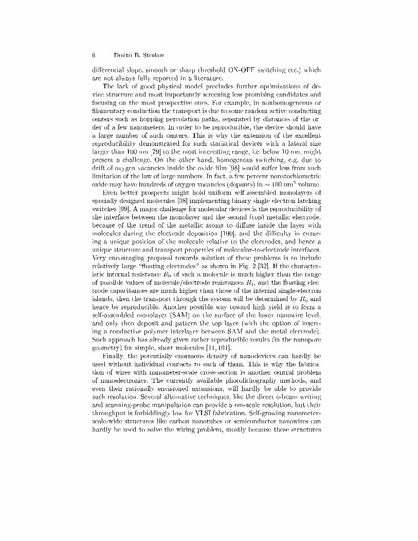
It is also clear that a shift of the nanowire/nanodevice subsystem by onenano-wiring pitch with respect to the CMOS base does not a�ect the circuitproperties. Moreover, a straightforward analysis of CMOL interface (Fig. 5)shows that at an optimal shape of the interface pins (for example, when topradius of both upper and lower level interface pins, the nanowire width andnanowire spacing are all equal) even a complete lack of alignment of thesetwo subsystems leads to a theoretical interface yield of 100%. (Note that thelast statement is only true for the latest version of CMOL [26, 29] in whichpin, going to the upper nanowire level, intentionally interrupts a lower layerwire - see Fig. 4.) Even if the interface yield will be less than 100%, it may beacceptable, taking into account that the cost of the nanosystem fabrication,including the chemically-directed assembly of molecular devices may be ratherlow, especially in the context of an unparalleled density of active devices inCMOL circuits.
More recently, several approaches to the interface between CMOS andnano subsystems, very similar to CMOL, have been proposed. In Ref. 126,interface between nano and CMOS wires is supposed to be formed by exposingportions of CMOS wires with precisely angled cut in the insulator layer (Fig.6). The key point in this proposal is that the interface yield can be up to100% without any overlay alignment between nano and CMOS layers if thevertical gap wgap between CMOS openings and its height are exactly equal tonanowire width wnano and nanowire spacing sspace, correspondingly. Clearly,the idea behind it is the same as that of CMOL, if one replaces CMOS areaopenings with CMOS pillars.
The advantage over CMOL approach is that the cut is much easier toimplement than the pins. On the other hand, this approach has also rather
12 Dmitri B. Strukov
fine
Shift along the top level:
Shift along the bottom level:
fine fine fine finebad!
fine fine fine finebad? bad!
Fig. 5. The idea of 100% CMOS-to-nano interface yield without any overlay align-ment.
wCMOS sCMOS
wcut
open cuts
CMOS wire
wgap
α insulator
nanowire (b)
(a)
snano
wnano
Fig. 6. The idea of 100% CMOS-to-nano interface yield without any overlay align-ment [126].
substantial disadvantages: (I) The interface density is more than twice lowerthat the maximum possible one; (II) the proposed interface is peripheral sincethe suggested technique only feasible for interfacing one layer of nanowires at atime. Hence, it may be used on the crossbar periphery rather than distributedover all the area as CMOL. As a result, the implementation of logic circuitsin this technology is hardly feasible (cf. Section 5).

Title Suppressed Due to Excessive Length 13
pin pad
pin CMOS
nano
CMOS
nano
FPNI
pin pin pin
CMOL
pad
Fig. 7. Comparison of CMOL and HP's FPNI circuits (adapted from Ref. 42).
The area interface without nanometer-scale pins is suggested recently inHP's FPNI circuits [42]. According to the authors, such FPNI circuits is ageneralization of the CMOL FPGA approach, allowing for simpler fabricationand more conservative process parameters. More speci�cally, authors indicatethat the sharply-pointed interface pins with nanometer-scale top radii presenta fabrication challenge and at the initial stage it is easier to replace them withCMOS-scale pins. For such change the nanowire crossbar requires CMOS-scalealignment with respect to CMOS subsystem and will be much sparser thanthe original used in CMOL (Fig. 7). Another feature that simpli�es fabri-cation of FPNI is the fact that nanodevices are used only as programmableresistance switches. The downside of FPNI approach is that more function-ality is transferred in CMOS subsystem and together with sparser nanowirecrossbar the areal density of FPNI logic circuits is substantially lower thanthat of CMOL-based ones [42]. The performance degradation is expected tobe much less in memories. For example, our preliminary results indicate thatdensity of FPNI-based memory is only about 50% less than that of originalCMOL ones [30].
Finally, very recently another promising concept based on CMOL idea wassuggested [25]. It is clear from Fig. 5 that the most challenging part in theinterface is connection to top layer nanowires. (Actually, the bottom layerinterface can be even further simpli�ed by choosing better pin geometry, e.g.,

14 Dmitri B. Strukovprolonging pin shape along the nanowire direction, without sacri�cing thedensity of the interface.) The suggested modi�cation of CMOL removes thischallenging part by placing top layer interface pins on the other side of crossbararray (Fig. 8). This requires stacking of two separately prepared CMOS dies,one with a set of parallel nanowires and device layer on top and another withperpendicular set of parallel nanowires. Clearly, due to the additional CMOSactive layer the performance of such CMOL circuits could be even furtherimproved [24] as compared to the ones based on the original CMOL concept.
nanodevices
nanowire crossbar
interface pins
CMOS stack
die 1
die 2 interface pins
CMOS stack
Fig. 8. 3D CMOL circuits [25].
4 CMOL MemoriesThe most straightforward application of crossbar CMOS/nanodevice hybridsis in memory circuits - see, e.g., theoretical proposals [18, 27, 30, 127] andthe �rst experimental demonstrations [64, 111, 116]. Note that such circuitscan be thought of as an extension of more general \crossbar" or \resistive"memory species. In particular, it includes very promising crossbar memorieswith CMOS-scale wires [56, 65, 128, 129], which have a potential to be thedensest among memories based on the conventional photolithography-basedtechnologies. This is why our discussion of these circuits is somewhat relevantfor a much wider types of memories.
In crossbar memories, nanodevices are used as a single-bit memory cells,while the semiconductor transistor subsystem performs all the peripheral (in-put/output, coding/decoding, line driving, and sense ampli�cation) functionsthat require relatively smaller number of devices (scaling as N1=2, where Nis the memory size in bits). If area overhead associated with periphery cir-cuits is negligible then the footprint of the crossbar memories can be as smallas (2Fnano)2, which might result in the unprecedented density in excess of1 Terabit/cm2 at the end of the hybrid technology roadmap (for Fnano = 3

Title Suppressed Due to Excessive Length 15nm), i.e. three orders of magnitude higher than that in existing semiconductormemory chips. 5
VREAD
Vout
A
+VWRITE
-VWRITE
A
(a) (b)
Fig. 9. Equivalent circuits of the crossbar memory array showing (a) read and (b)write operations for one of the cells (marked A). On panel (a), green arrow showsthe useful readout current, while red arrow shows the parasitic current to the wrongoutput wire, which is prevented by the nonlinearity of the I � V curve of device A(if the output voltage is not too high, Vout < Vt).
The basic operation of crossbar memories can be explained using simpli�edequivalent circuits shown on Fig. 9. In the low-resistive state presenting binary1, the nanodevice is essentially a diode, so that the application of voltage Vt <VREAD < V+ to one (say, horizontal) nanowire leading to the memory cell givesa substantial current injection into the second wire (Fig. 9a). This currentpulls up voltage Vout which can now be read out by a sense ampli�er. Thediode property to have low current at voltages above �Vt prevents parasiticcurrents which might be induced in other state-1 cells by the output voltage -see the red line in Fig. 9a. On the other hand, it is easy to show that memoryarrays with purely linear (resistive) nanodevices do not scale well and hardlypractical [130].
In state 0 (which presents binary zero) the crosspoint current is very small,giving a nominally negligible contribution to output signals at readout. Inorder to switch the cell into state 1, the two nanowires leading to the deviceare fed by voltages �VWRITE (Fig. 9b), with VWRITE < V+ < 2VWRITE. (Theleft inequality ensures that this operation does not disturb the state of \semi-selected" devices contacting just one of the biased nanowires.) The write 0operation is performed similarly using the reciprocal switching with threshold
5Here, we do not include in our comparison the data storage systems (such ashard disk drives, etc.) which cannot be used for bit-addressable memories becauseof their very large (millisecond-scale) access time.

16 Dmitri B. StrukovV- (Fig. 1). It is evident from Figs. 9a, b that the read and write operationsmay be performed simultaneously with all cells of one row.6
The two main approach for �ghting errors in semiconductor memory tech-nology is recon�guration, i.e. the replacement of memory array lines (rows orcolumns) containing bad cells by spare lines [131,132]. The e�ectiveness of thereplacement depends on how good its algorithm is [132,133]. The ExhaustiveSearch approach (trying all possible combinations) �nds the best repair solu-tion, though it is not practicable because of the exponentially large executiontime. A more acceptable choice is the \Repair Most" method that allows asimple hardware implementation and an execution time scaling linearly withthe number of bits. In this approach, the number of defects in each line of amemory block (matrix) is counted, and the lines having the largest numberof defects are replaced with a spare lines.
For a larger fraction of bad bits, better results may be achieved [18,112,134]by combining the bad line exclusion with ECC techniques. The simulation re-sults for application of such technique for crossbar hybrid memories [18, 112]have shown that defect tolerance up to � 10% may be achieved using verypowerful ECC, e.g. Reed-Solomon and Bose-Chaudhuri-Hocquenghem (BCH)codes [135]. Unfortunately, in those works, the contributions of the circuits im-plementing these codes to the memory access time (which for some codes maybe extremely large) and the total memory area have not been estimated. Alsothe account of the �nite leakage current through nominally closed crosspoints(which was neglected in Ref. 18) may change the memory scaling rather sub-stantially [117]. What follows is the review of our own approach to terabit-scaledefect tolerant CMOL-based nanoelectronic memories, where we included allrelevant overheads in our estimations.
Figure 10a shows the assumed general structure of the CMOL memory.Essentially, it is similar to that of the conventional memories, i.e. it is a rect-angular array of L crosspoint memory banks (\blocks"), so that during asingle operation, a particular row of CMOL blocks is accessed with the helpof block address decoders. In contrast, the block architecture (Fig. 10b) isspeci�c for the CMOL interface which allows the placement of CMOS \relay"cells under the nanowire crossbar. These cells are controlled by CMOS-leveldecoders, four per each block (Fig. 10b). At each elementary operation, onepair of block decoders (shown in magenta in Fig. 10b, as well as in Figs. 11and 12a below) addresses one vertical and one horizontal CMOS line, andthus selects a certain relay cell at their crosspoint. This cell (Fig. 12a) appliesthe data signal to a \red" interface pin contacting a bottom-layer nanowire.The other pair of decoders (shown in violet in Figs. 10b, 11, and 12a) selectsa set of di�erent relay cells which provide similar biasing of the corresponding
6Actually, only one of the \write 0" and \write 1" operations can be performed si-multaneously with all cells. Because of the opposite polarity of the necessary voltagesacross nanodevices for these two operations, the complete write may be implementedin two steps, e.g., �rst writing 0s and then writing 1s.

Title Suppressed Due to Excessive Length 17
(a)
cell addresses
block row address
data I/O
block address decoder
block
block
block
block
block
block
block
block
block
(b)
select decoder
data I/O
external address
memory cell array
select decoder
address control
mapping table
data decoder
data decoder
Acol1
Acol2
Arow2
Arow1
ECC unit
Fig. 10. CMOL memory structure: (a) global and (b) block architectures.
top level nanowires through \blue" pins. These nanowires may now address allcrosspoint nanodevices (memory cells) of a particular nanowire segment. Thusthe four decoders of the block, working together, can provide every memorycell of the segment with voltages necessary for the read and write operations.
The remaining circuitry shown in Fig. 10b, i.e. CMOS-based mapping ta-ble and address control circuits, is needed to convert the logical (external)addresses, which are fed to the CMOL blocks, into internal addresses of mem-ory cells inside the block. In particular, the mapping table converts the logicaladdress of the segment (which is the same for all selected blocks) into a pairof block-speci�c physical addresses, Acol1 and Arow1, and CMOS-implementeddecoders activate the corresponding CMOS-level lines.
Figure 11 shows the low-level structure of the CMOL memory for a par-ticular (unrealistically small) values of the block size and the main topologi-cal parameter of CMOL, a = 4. The top-level nanowires (here shown quasi-horizontal) stretch over the whole block, but the low-level (nearly-vertical)nanowires are naturally cut into segments of equal length. An elementaryanalysis of the CMOL geometry (Fig. 4) shows that each nanowire segmentstretches over a CMOS cells and contacts a2 (in Fig. 11, sixteen) crosspointnanodevices.
Signals Acol1 and Arow1 are applied to CMOS wires, feeding the \red" linesof the corresponding CMOS-implemented relay cells (Fig. 12a). By opening allpass transistors of the row, Arow1 selects a speci�c \red" pin of column Acol1,so that the data Acol1 are fed only to a speci�c nanowire segment contactinga2 crosspoint nanodevices. In parallel, addresses Acol1 and Arow1 are sent tothe CMOS-based address control circuitry to generate another pair of physicaladdresses Arow2 and Acol2. Signal Arow2 opens the \blue"-pin pass transistorsin relay cells of a row, and thus connects each of a2 quasi-horizontal nanowires

18 Dmitri B. Strukov
select
select
Arow1
Arow2a
Arow2b
data Acol1
select
select
Arow1
Arow2a
select
Arow2b
data (a2 lines)
data Acol1
(a)
(b)
barrel shifter
barrel shifter
data (a2 lines)
select
Acol2
Acol2
Fig. 11. CMOL block architecture: Addressing of an interior column of nanowiresegments (for a = 4). The �gure shows only one (selected) column of the segments,the crosspoint nanodevices connected to one (selected) segment, and continuous top-level nanowires connected to these nanodevices. (In reality, the nanowires of bothlayers �ll all the array plane, with nanodevices at each crosspoint.) The block arrowsindicate the location of CMOS lines activated at addressing the shown nanodevices.

Title Suppressed Due to Excessive Length 19of the top layer to a speci�c CMOS lines (shown purple), thus enabling a reador write operation.
Our defect tolerance is based on the synergetic approach where memoryarray recon�guration is combined with ECC [134].7 In order to implement thismemory cells are divided into fragments of certain size (\granularity"). Eachof these fragments is tested using ECC circuitry, and those of them which maynot be ECC-corrected are excluded from operation. (For that, the addressesof good fragments are written into the mapping table, see Fig. 10b). If thefraction q of bad bits is large, the large granularity of exclusion is impracti-cable, due to the exponential growth of the number of necessary redundantresources. On the other hand, �ne granularity requires an unacceptably largemapping table. This is why we have used a very exible approach when thegranularity of exclusion is not related to the physical structure of the memoryarray. This means that the data fragment length, equal to g nanowire seg-ments (i. e. ga2 memory cells) may be either smaller or larger than the onesegment (which has a2 memory cells).
Requiring that the total yield Y is �xed at a certain level and using detailedperformance model [30] we have calculated the total chip area A necessaryto achieve a certain useful bit capacity N , and hence the area per useful bit,A=N . The last number, normalized to the CMOS half-pitch area,
a � AN(FCMOS)2 ; (2)
is a very convenient �gure of merit that depends only on the ratio FCMOS=Fnanorather than on the absolute parameters of the fabrication technology.Figure 13 presents typical �nal results8 of our optimization procedure,
carried out for several values of the total access time. (For our parametersthe access time is dominated by the ECC decoding, while intrablock and in-terblock latencies are negligible.) The cusps on the curves are due to suddenchanges of discrete parameters (ga2, and the number of total and informationbits in ECC) for which the largest memory density is achieved. In particular,Fig. 13 shows that CMOL memories may become denser than purely CMOSones at the fraction of bad bit devices as high as � 15 if the latency require-ment is not too small (i.e. > 10 nm) for both considered cases of pitch ratio.On the other hand, to reach 5� and 10� advantage in density such fractionof bad bits should be below 5% and 2% for FCMOS=Fnano = 3:3 and 10 pitchratios, correspondingly.
7We have only considered \stuck-on-open" kind of defects in this work. It isworth mentioning that considered architecture is very e�cient for tolerating allother types of defects (e.g., broken or shorted nanowires), except for \stuck-on-close" (permanently shortened) nanodevices.8Though formally the results depend on the total memory size N and yield Y ,they are rather insensitive to these parameters in the range of our interest (N � 1012bits, Y � 90%). As Fig. 13 shows, the required memory access time � also has amarginal e�ect on density, provided that � is not too small.

20 Dmitri B. Strukov (a) (b)
CMOS column 1
CMOS column 2
CMOS row 2
CMOS row 1
input nanowire
output nanowire
CMOS inverter
2βFCMOS
in
CMOS column 1
CMOS column 2
CMOS row 2
CMOS row 1
CMOS latch
4βFCMOS
(d) CMOS column 1
CMOS column 2
CMOS row 2
CMOS row 1
input nanowire (not used)
output nanowire
2βFCMOS
CMOS pass gate
CMOS control
(f)
1 2 3
4 5 6
7 8 9
6βFCMOS
all output pins
input pins 1, 3, 7, 9
input pins 2, 4, 5, 6, 8 OE
clk
in out
OS
ON
OW
IS
IE
IW
IN CN CE CS CW
SEL
data
Arow1 select
input nanowire
output nanowire
2βFCMOS
Rpd
data Acol1
Arow2 select
(c)
out
(e)
Fig. 12. Possible structure of CMOL cells: (a) memory relay cell; (b) the basic cell,and (c) the latch cell of CMOL FPGA; and (d) control cell, and (e, f) programmablelatch cell of CMOL DSP. Here red and blue points indicate the corresponding in-terface pins. For the sake of clarity panels (a-e) shows only nanowires which arecontacted by interface pins of the given cells. Also for clarity, panel (e) shows onlythe con�guration circuitry, while panel (f) shows the programmable latch implemen-tation.

Title Suppressed Due to Excessive Length 21
10-5 10-4 10-3 10-2 10-1 10010-1
100
101
FCMOS/Fnano=3.3
Ideal CMOL
Ideal CMOS
Access time (ns) 3 10 30 100
Fraction of bad nanodevices, q
Are
a pe
r use
ful b
it, a =
A/N
(FC
MO
S)2
10-5 10-4 10-3 10-2 10-1 10010-2
10-1
100
101
FCMOS/Fnano=10
Ideal CMOS
Are
a pe
r use
ful b
it, a =
A/N
(FC
MO
S)2
Fraction of bad nanodevices, q
Access time (ns) 3 10 30 100
Ideal CMOL
(a)
(b)
Fig. 13. The total chip area per one useful memory cell, as a function of the badbit fraction q, for several values of the memory access time and two typical values ofthe FCMOS=Fnano ratio. The horizontal lines indicate the area for \perfect" CMOSand CMOL memories. In the latter case, this line shows our results for negligible q,while for the former case we use the ITRS data [3] for the densest semiconductor( ash) memories.

22 Dmitri B. StrukovNote, however, that our optimistic results for the memory speed are based
on the fundamental physical limitations for the crosspoint nanodevice param-eters, in particular, RON, which was of the order of few Ks. For the currentlyimplemented programmable diodes, the picture is somewhat di�erent. For ex-ample, for the simple and reproducible CuOx devices [79], scaled down toFnano = 3 nm, the e�ective value of RON=D would be � 2 M, resulting inintrablock latency of about 50 ns. This means that our results (Fig. 13) woulddegrade only slightly. On the other hand, for the demonstrated reproduciblemolecular monolayers [101], typical RON=D of a similarly scaled crosspointdevice would be in the G range, so that the memory speed would be muchlower. Nevertheless, a considerable progress of the improvement of molecularprogrammable diodes during the next few years may be readily anticipated.
5 CMOL FPGA CircuitsThe practical techniques for high defect tolerance in digital (Boolean) logicis less obvious. In the usual custom logic circuits the location of a defectivegate from outside is hardly possible, while spreading around additional logicgates (e.g., providing von Neumann's majority multiplexing [136]) for errordetection and correction becomes very ine�cient for fairly low fraction q ofdefective devices. For example, even the recently improved von Neumann'sscheme requires a 10-fold redundancy for q as low as � 10�5 and a 100-foldredundancy for q � 3� 10�3 [137].
This is why the most signi�cant previously published proposals for theimplementation of logic circuits using CMOL-like hybrid structures had beenbased on recon�gurable regular structures like the �eld-programmable gatearrays (FPGA). Before this work, two FPGA varieties had been analyzed,one based on look-up tables (LUT) and another one using programmable-logic arrays (PLA).
In the former case, all possible values of an m-bit Boolean function ofn binary operands are kept in m memory arrays, of size 2n � 1 each. (Form = 1, and some representative applications the best resource utilizationis achieved with n close to 4 [138], while the famous recon�gurable computerTeramac [115] is using LUT blocks with n = 6 and m = 2.) The main problemwith this approach is that the memory arrays of the LUTs based on realisticmolecular devices cannot provide address decoding and output signal sensing(recovery). This means that those functions should be implemented in theCMOS subsystem, and the corresponding overhead may be estimated usingour results discussed in the previous section. Using the results from Section 4one can show that for the memory array with 26�2 bits, performing the func-tion of a Teramac's LUT block, and for a realistic ratio FCMOS=Fnano = 10 thearea overhead would be above four orders of magnitude (!), and would evenloose the density (and hence performance) competition to a purely-CMOS cir-cuit performing the same function. On the other hand, increasing the memory

Title Suppressed Due to Excessive Length 23array size to the optimum is not an option, because the LUT performancescales (approximately) only as a log of its capacity [138].
The PLA approach is based on the fact that an arbitrary Boolean functioncan be re-written in the canonical form, i.e. in the two-level logical representa-tion. As a result, it may be implemented as a connection of two crossbar arrays,for example one performing the AND, and another the OR function [33]. The�rst problem with the application of this approach to the CMOS/nanodevicehybrids is the same as in the case of LUT's: the optimum size of the PLAcrossbars is �nite, and typically small [139], so that the CMOS overhead isextremely large. Moreover, any PLA logic built with diode-like nanodevicesfaces an additional problem of high power consumption. In contrast with LUTarrays, where it is possible to have current only through one nanodevice ata time, in PLA arrays the fraction of open devices is of the order of onehalf [36]. Let us estimate the static power dissipated by such an array. Thespeci�c capacitance of a wire in an integrated circuit is always of the orderof 2� 10�10 F/m [28]. With Fnano = 3 nm, this number shows that in orderto make the RC time constant of the nanowire below than, or of the order ofthe logic delay in modern CMOS circuits (�10�10s), the ON resistance RONof a molecular device has to be below � 7 � 107 ohms. For reliable opera-tion of single-electron transistor (and apparently any other active electronicnanodevice) at temperature T , the scale VON of voltage across it has to beat least 10kBT [1]. For room temperature this gives VON > 0:25 Volt, so thatstatic power dissipation per one open device, PON = V 2ON=RON is close to 10nW. With the open device density of 0:5=(2Fnano)2 � 1012 cm�2, this createsa power dissipation density of at least 10 kW/cm2, much higher than thecurrent and prospective technologies allow to manage [3].
As a matter of principle, power consumption may be reduced by usingdynamic logic, but this approach requires more complex nanodevices. Forexample, Refs. 17, 35 describe a dynamic-mode PLA-like structure (with im-proved functional density via wrapped logic mapping) using several typesof molecular-scale devices, most importantly including �eld-e�ect transistorswhich are formed at crosspoints of two nanowires. In such transistor, one(semiconductor) nanowire would serve as a drain/channel/source structure,while the perpendicular nanowire would play the role of the gate. Unfor-tunately, such circuits would fail because of the same fundamental physicalreason that provides the fundamental limitation to the Moore's Law: anysemiconductor MOSFET with a-few-nm-long channel is irreproducible be-cause of exponential dependence of the threshold voltage on the transistordimensions [140].9 Similar problems are likely to prevent hybrid circuits de-
9In principle, this problem can be alleviated by making the width of nanowires inone dimension comparable with that of lithographically de�ned wires [35]. However,that also means that such hybrid circuits cannot take full advantage (only in onedimension) of nanodevice nanometer-scale footprints.

24 Dmitri B. Strukovscribed in Refs. 15,113 from scaling down beyond 10-nm range, since they arebased on nanoscale FETs.
Finally, the last signi�cant category of suggested crossbar hybrids includescircuits based on Goto-pair logic [33]. In particular, Refs. 22, 44 describe anarchitecture where Goto-pair logic is implemented with two-terminal resistivecrossbar latches [45]. The main architectural challenge of this approach is dueto the fact that nanodevice bistability is employed during Goto pair operation.10 Since the assumed nanodevices have no third state, and hence, cannot beenabled or disabled, it is unclear how to map a particular circuit on sucharchitectures. (Having a third state would be more challenging since multi-state devices are not very reliable.)
Moreover, the use of bistability in the circuit operation is rather imprac-tical due to the relation between the retention time and the switching speedin the crossbar latches. In order to be useful for most electronics applications,the latches should be switched very fast (in a few picoseconds in order to com-pete with advanced MOSFETs), but retain their internal state for the timenecessary to complete the calculation (ideally, for a few years, though severalhours may be acceptable in some cases). This means that the change of theapplied voltage by the factor of two (the di�erence between the fully selectedand semi-selected crosspoints of a crossbar) should change the switching rateby at least 16 orders of magnitude. However, even the most favorable physicalprocess we are aware of (the quantum-mechanical tunneling through high-quality dielectric layers like the thermally-grown SiO2) may only produce,at these conditions, the rate changes below 10 orders of magnitude, even ifuncomfortably high voltages of the order of 12 V are used [141].
Let us now discuss an alternative approach to Boolean logic circuits basedon CMOL concept [26,28,29], that is closed to the so-called cell-based FPGA[142]. We have studied two varieties of CMOL FPGA fabrics [26,28,29]. Thearchitecture of the simplest variety, one-cell fabric [28], is very convenientfor elaborating the concept and basic properties of CMOL FPGA, though itcannot be used for sequential circuit design. On the other hand, a two-cellfabric [26, 29], which is a generalization of the single cell structure, can beused for mapping arbitrary circuits, and all simulation results in this sectionwe will be given for a such variety of CMOL FPGAs.
Figure 14 shows a fragment of one-cell CMOL FPGA fabric. Essentially, itis a uniform structure which is built by replicating \basic" cells with an areaA = (2�FCMOS)2. In this case, the angle � is given by the generic formula forCMOL, i.e. tan� � 1=a (Eq. 1), where a is an integer de�ning the range of cellinteraction (Fig. 14).11 For �xed fabrication technology parameters FCMOS,
10As a reminder, in all discussed crossbar circuits above, as well as in our approachfor Boolean logic described in this section and Section 6), the state of nanodevicesremains unchanged during circuit operation.11Note that even though the nanowire crossbar in Ref. 28 was rotated by theadditional 45� angle, which was convenient for manual mapping, it does not a�ectthe performance results.

Title Suppressed Due to Excessive Length 25
(a) α 2βFCMOS 2βFCMOS×a
(b) 2βFCMOS×a
2Fnano
2aFnano
2(βFCMOS)2
Fnano
Fig. 14. The fragment of one-cell CMOL FPGA fabric for the particular case a = 4.In panel (a), output pins of M = a2 � 2 = 14 cells (which form so-called input cellconnectivity domain) painted light-gray may be connected to the input pin of aspeci�c cell (shown dark-gray) via a pin-nanowire-nanodevice-nanowire-pin links.Similarly, panel (b) shows cells (painted light gray) whose inputs may be connecteddirectly to the output pin of a speci�c cell (called output connectivity domain).

26 Dmitri B. StrukovFnano, and �min, the lower bound on a is given by inequality:
a2 > (�minFCMOS=Fnano)2 � 1: (3)Each basic cell (Fig. 12b) consists of an inverter and two pass transistors
that serve two pins (one of each type) serving as the cell input and output,respectively. During the con�guration stage, all inverters are disabled by anappropriate choice of global voltages VDD and Vgnd (Fig. 12b), and testingand setting of all nanodevices is carried out absolutely similarly to memorywrite operation described in previous section.
In contrast with CMOL memories, nanowires in upper layer are also fabri-cated with small breaks repeated with period L = 2(�FCMOS)2=Fnano. Withthis arrangement, each nanowire segment is connected to exactly one inter-face pin.12 As a result, each input or output of a basic cell can be connectedthrough a pin-nanowire-nanodevice-nanowire-pin link to each of
M = a2 � 2 (4)other cells located within a square-shaped \cell connectivity domain" aroundthe initial cell - see Fig. 14. (For in�nitesimal gaps, M would equal a2 � 1,but for a more feasible gap width of the order of 2Fnano, the connectivitydomain is by one cell smaller.) Note that in reality both input and output cellconnectivity domains would be much larger than those shown in Fig. 14 forpractical values of a > 10 and have the same roughly square shape (with someprotrusions of the cells on the perimeter of the domain). This fact simpli�esthe design automation for CMOL FPGA circuits [26].
When the con�guration stage has been completed, the pass transistors areused as pull-down resistors, while the nanodevices set into ON (low-resistive)state are used as pull-up resistors. Together with CMOS inverters, these com-ponents may be used to form the basic \wired-NOR" gates (Fig. 15). Forexample, if only the two nanodevices shown in a Fig. 15b are in the ON state,while all other latching switches connected to the input nanowire of cell Hare in the OFF (high resistance) state, then cell H calculates NOR functionof signals A and B. Clearly, the gates with high fan-in (Fig. 15c) and fan-outor broadcast (Fig. 15d) may be readily formed as well by turning ON thecorresponding latching switches. Having these primitives is su�cient to im-plement any Boolean function, as well as to perform routing, providing thatthe hardware resources are su�cient.
12The best performance is achieved if the pin contacts the wire fragment in itsmiddle, and our analysis has been carried out with this assumption. Since lower layernanowire segments are cut by upper layer pins, a connection exactly in a center iseasily achievable, i.e. by locating upper level pins correspondingly. For upper layerpins, a similar trick can be done, if upper layer nanowire breaks are provided byfeatures of the same lithographic mask that de�nes interface pin positions. Alsonote, that a modest misalignment of the pin and the breaks (by � FCMOS) reducesthe circuit performance only by a small factor of the order of 1=� � 1.

Title Suppressed Due to Excessive Length 27
H
A B
CMOS inverter
nanodevices
pass transistor
A H
RON
Rpass Cwire
B
A
H
(b) (a)
B A
H
E
D G
F
C
A B C D E F G
H
B
(c)
A
B
C
D
H B
A
H
D
C
(d)
Fig. 15. Logic and routing primitives in CMOL FPGA circuits: (a) equivalentcircuit of fan-in-two NOR gate, (b) its physical implementation in CMOL, (c) theexample of 7-input NOR gate and (d) the example of fan-out of signal to four cells.Note that only several (shown) nanodevices on the input nanowires in panels (b),(c), and output nanowire in panel (d) of cell H are set to the ON state, while others(not shown) are set to the OFF state. Also, for the sake of clarity panels (b), (c),and (d) shows only the nanowires used for the gate and the broadcast.

28 Dmitri B. Strukov
tile boundary latch cell basic cell
2βFCMOS
2Fnano
2aFnano
α
interface pin to bottom layer nanowires
interface pin to upper layer nanowires
program- mable latch cell
tile
control cell
basic cells
2βFCMOS
2aFnano
interface pin to a bottom layer nanowire
interface pin to an upper layer nanowire
2Fnano
α
(a)
(b)
Fig. 16. A fragment of (a) two-cell CMOL FPGA fabric and (b) three cell CMOLDSP fabric for the particular case a = 4.

Title Suppressed Due to Excessive Length 29
4×A×2βFCMOS 4×2βFCMOS
I
O1
O2
R
Fig. 17. Tile connectivity domain: Any cell of the central tile (shown dark gray)can be connected with any cell in the tile connectivity domain (shown light gray) viaone pin-nanowire-nanodevice-nanowire-pin link (e.g., cells I and O1). Cells outsideof each other's tile connectivity domain (e.g., I and O2) can be connected withadditional routing inverters (e.g., R). Note that nanowire width and nanodevice sizeare boosted for clarity. For example, for the considered CMOL parameters, 1600crosspoint nanodevices may �t on one basic cell area.
SIS: Technology (NOR gates and latch)
Input circuit blif format
Initial value of K
Heuristic placement
Global router
Exit with success
Increase K
countmax < T-K -∆ countmax > T-K K = 0
Circuit processing
Defective cells
Decrease K
otherwise
Exit without success
Detail router Defective nanodevicefailed
passed
Fig. 18. CMOL FPGA design ow used in this work.
30 Dmitri B. StrukovA genuine optimization of CMOL FPGA circuit architectures would re-
quire a completely new set of CAD tools, whose development is a challengingtask. At this preliminary stage, our choice was instead to get as much lever-age as possible from the existing ideas and algorithms used for mapping andarchitecture exploration of semiconductor logic, in particular, from the designautomation algorithms for island-type CMOS FPGAs [143].
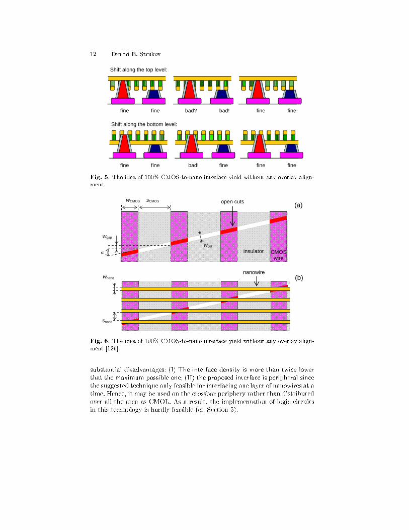
In order to use such design automation algorithms, we have restricted ourdesign to a speci�c, simple two-cell-species CMOL fabric. The fabric is a uni-form mesh of square-shaped \tiles" (Fig. 16a). Each tile consists of a shellof T basic cells (Fig. 12c) surrounding a single \latch" cell (Fig. 12d). Thelatter cell is just a level-sensitive latch implemented in the CMOS subsys-tem, connected to 8 interface pins, plus two pass transistors used for circuitcon�guration. Note that all four pins of each (either input or output) groupare always connected, so that the nanowires they contact always carry thesame signal. This means that at con�guration, groups of four nanodevices sit-ting on these wires may be turned on or o� only together. A simple analysisshows that this does not impose any restrictions on the CMOL FPGA fabricfunctionality.
The convenience of the proposed two-cell CMOL FPGA structure is that,from the design point of view, the CMOL tile can be treated in the sameway as that of the island-type CMOS FPGA. To demonstrate that let us �rstintroduce a very useful concept of \tile connectivity domain" which makesrouting of CMOL FPGA circuits similar to CMOS FPGA ones. Similarlyto the cell connectivity domain, the tile connectivity domain of a given tile isde�ned as such fabric fragment that any cell within it can be connected to anycell of the initial tile directly, i.e. via one pin-nanowire-nanodevice-nanowire-pin link (Fig. 17). Just as for cell connectivity domains all tile connectivitydomains are similar and have square shape. (Note that we assume that inputand output tile connectivity domain are the same.) The linear size A of thetile connectivity domain for the assumed tile size T = 16 can be found as
A = 2ba=8c � 1: (5)For instance, Fig. 17 shows a tile connectivity domain for the case A = 5: (Inmore realistic cases a = �FCMOS=Fnano � 40, i.e. A � 9.)
The main idea of the proposed design ow for CMOL FPGAs (Fig. 18)is to reserve some number of basic cells (T �K) inside each tile for routingpurposes, while use the rest (K) cells for logic during the placement step. Theplacer tries to put gates into such locations (with maximum one latch andK NOR gates per tile) so that their interconnect is local or, equivalently, iswithin tile connectivity domain of each other. At the global routing step, idlecells inside each tile are used to interconnect global connections. If there isa congestion after the global routing step, i.e. the number of requested basiccells during routing countmax is larger than the actual number of idle cellsT � K � � (here � is parameter which allows to trade-o� the number of

Title Suppressed Due to Excessive Length 31iterations with the mapping quality), then we decrease K and repeat the owagain until there is no congestion.
We have applied our methods to analyze possible CMOL FPGA imple-mentation of the Toronto 20 benchmark circuit set [144]. Using the completelycustom design automation ow [26, 29] we have �rst mapped the circuits onthe two-cell CMOL FPGA fabric. Then, assuming a plausible power supplyvoltage VDD = 0.3 V [29], we �nd the smallest acceptable nanodevice resis-tances, and consequently the lowest delay of CMOL gates, such that the powerconsumption density does not exceed the ITRS-speci�ed value of 200 W/cm2and the voltage swing on the input of CMOS inverters is su�ciently largerthan the corresponding shot and thermal noise of nanodevices [28, 29]. Fromsuch optimization the crosspoint resistance in the ON state is about 280 K,while delay �0 of a NOR-1 gate is about 80 ps.
Table 1 summarizes the performance results for the benchmark circuitsmapped on CMOL FPGA without any defects. Note that in contrast withearlier nanoelectronics work, the results for di�erent circuits are obtainedfor the CMOL FPGA fabric with exactly the same operating conditions andphysical structure for all the circuits, thus enabling a fair comparison withCMOS FPGA. For this comparison, the same benchmark circuits have beensynthesized into cluster-based island-type logic block architecture [143] andscaled (using very optimistic assumptions) to get CMOS FPGA performancefor similar CMOS technology node [28]. Also, for a comparison we show inTable 1 the simulation results for NanoPLA concept presented in Ref. 118.
Finally, our simulations have shown that the CMOL FPGA is very re-silient to various types of defects [26,28]. For example, �gure 19b shows thatat realistic parameter a = 40 circuits may have a fabrication yield above 99%with up to 20% of stuck-on-open nanodevices [28]. Such high defect toleranceshould not be surprising because only a small percent of nanodevices (about0.1% of the total on average) is utilized. A huge redundancy can be e�cientlyexploited by the detail routing algorithm, which allows to pick completelydeferent set of nanodevices by moving positions of the gates [28]. Indeed, insome cases successful recon�guration around as many as 50% of bad nanode-vices is possible (Fig. 19a). Also, our simulations have shown that the CMOLFPGA is very resilient to defective CMOS cells [26]. In particular, the aver-age swelling of the circuit area is rather limited: only about 20% and 80%for 10% and 30%, respectively, uniformly distributed defective cells (see, e.g.,Figure 20). This means that faulty interface pins, nanowires and/or CMOScircuitry can be very e�ectively tolerated. On the other hand, the toleranceto stuck-on-close crosspoint defects is rather low (equivalent to about 0.02%of defective nanodevices for 30% defective cells, so that some other defecttolerance mechanism should be used to reduce the e�ects of such faults.

32 Dmitri B. Strukov
1
0.01 0.1 10
20
40
60
80
100
1E-5 1E-4 1E-3 0.01 0.1 190
99
1E-3
99.99
0.01 0.1 10
20
40
60
80
100
Bad Nanodevice Fraction q
r'=17, r = 17
r'=10, r = 10 11 12 13
Circ
uit Y
ield
Y (%
)Bad Nanodevice Fraction q
r'=10 r=12
r'=10, r=10
crossbar adder
99.9
Circ
uit Y
ield
Y (%
)
r'=17, r= 17 18 19
r'=10, r= 10 11 12
Circ
uit Y
ield
Y (%
)
Bad Nanodevice Fraction q
(b)
(a)
Fig. 19. (a) A small fragment of the 32-bit Kogge-Stone adder mapped on one-cellCMOL fabric after the recon�guration as around 50% stuck-on-open nanodevices.Bad nanodevices are shown black, good used devices green, unused devices are notshown, for clarity. Colored circles are only a help for the eye, showing the locationof interface pins (red and blue points) and used nanodevices. Thin vertical andhorizontal lines show CMOS cell borders. (b) The �nal (post-recon�guration) defecttolerance of 32-bit Kogge-Stone adder and the 64-bit full crossbar for several valuesof FCMOS=Fnano. For more details - see Ref. 28.

Title Suppressed Due to Excessive Length 33
CMOS FPGA (FCMOS = 45 nm)
CMOL FPGA (FCMOS = 45 nm, Fnano = 4.5 nm, max fan-in = 7)
Comparison
Circuit
Area (μm2)
Delay (ns)
Area (μm2)
Delay (ns)
ACMOS /ACMOL
AnanoPLA /ACMOL
alu4 137700 5.1 1004 4.0 137 0.28
apex2 166050 6.0 914 4.6 182 3.09
apex4 414619 5.5 672 3.6 617 0.58
bigkey 193388 3.1 829 2.7 233 1.82
clma 623194 13.1 9308 10.2 67 1.74
des 148331 4.2 1097 4.5 135 3.21
diffeq 100238 6.0 1194 10.4 84 2.27
dsip 148331 3.2 829 3.4 179 1.63
elliptic 213638 8.6 4581 12.7 47 1.63
ex1010 391331 9.0 3486 5.7 112 0.28
ex5p 100238 5.1 829 4.3 121 0.19
frisc 230850 11.3 4199 17.6 55 2.64
misex3 124538 5.3 1004 3.6 124 0.56
pdc 369056 9.6 4979 6.8 74 0.15
s298 166050 10.7 829 8.1 200 1.33
s38417 462713 7.3 9308 7.2 50 1.24
s38584 438413 4.8 9872 8.8 44 -
seq 151369 5.4 1296 4.0 117 1.15
spla 326025 7.3 2994 5.8 109 0.12
tseng 78469 6.3 1194 11.5 66 2.48 Table 1. Performance results for Toronto 20 benchmark set mapped on two-cellCMOL fabric with no defects.
6 CMOL DSP CircuitsIn general, any type of Boolean logic circuits can be mapped on CMOL FP-GAs. With several modi�cations CMOL FPGA can be turned into a circuitarchitecture which is especially e�cient for a very important class of applica-tions - low-level image processing tasks. (Such low-level tasks are performedfrequently in spatial �ltering, edge detection, feature extraction, etc. and typ-ically present a bottleneck in image processing systems.) More speci�cally, letus discuss possible performance of such circuits on a simple but representativeexample of 2D image convolution:
Tx;y =FXi=1
FXj=1
Sx+i;y+j'i;j ; (6)

34 Dmitri B. Strukov
latch primary input
NOR gate
routing inverter
primary output
defective cell
idle cell
Fig. 20. Example of mapping on two-cell CMOL fabric with a presence of defec-tive cells: dsip.blif circuit of the Toronto 20 set, mapped on the (21+2)�(21+2)tile array with 30% defective cells. Here the additional layer of tiles at the arrayperiphery is used exclusively for I/O functions. The cells from these peripheral tilesare functionally similar to input and output pads and cannot be con�gured to NORgates.
where S and T are input and output images, correspondingly, with N�Npixels each, and ' is a F�F pixel �lter function. Though sometimes specialrules for calculating the edge pixels of image T are used [4], we will considera simpli�ed version of the algorithm where the linear size of output image issmaller by (F � 1) pixels (Fig. 21), so that all output signals T are calculatedaccording to Eq. (6). Such simpli�cation should not a�ect the performanceresults for more general case since, typically, F � N . For example, the baselineparameters used for estimates in this work are F = 32, N = 1024, with the

Title Suppressed Due to Excessive Length 35similar accuracy (nS = nT = n' = n = 12 bits) of the input, output, and�lter data.
S plane (input) T plane (output) pixel
N
N
F
F
N – F + 1
Fig. 21. Scheme of the 2D image convolution for particular (impracticably small)sizes of the initial image (N = 16), and �lter window (F = 5).
Figure 22 shows the top-level architecture of the proposed CMOL-basedDSP. Here we assume the most challenging I/O option when the data are fedto, and picked up from the array from the periphery, e.g., the right side on theFig. 22. (If an area-distributed, 2D I/O is available, the circuit performancewould only be better.) The key part of the architecture, the CMOL array,is similar for each pixel. The pixel area is organized into a uniform mesh ofsquare-shaped \tiles" (Fig. 16). The number of tiles per pixel depends onthe data word length n; in our case it is close to 12�12. Each tile consistsof 26 basic cells, one control cell of the similar size, and one programmablelatch cell of a larger area (Fig. 16b). Just like in circuits discussed above theCMOS circuitry of each cell type is di�erent (see Fig. 12b, d, e, f), but theinterface and nanowire levels are the same for all cell types: similarly locatedpins of each elementary cell contact nanowire fragments of the same length.The CMOS-implemented con�guration circuitry, comprised of a pair of signallines (shown blue and magenta in Fig. 12b, d, e) and a pass transistor perpin, is also similar for each cell.
There are two new types of cells. The control cell (Fig. 12d) connects itsoutput nanowire to the CMOS control unit memory (outside the CMOL array)via the designated CMOS control lines [8]. The programmable latch cell (Figs.12e, f) is designed to provide not only temporary data storage but also a fast(CMOS-wire) interconnect between each tile and its four nearest neighbors -see inputs IS, IN, IW, IE and outputs OS, ON, OW, OE in Fig. 12f. The latter

36 Dmitri B. Strukov
Fig. 4
Test
/Con
figur
e
Control Unit
CMOL ARRAY
Test/Configure
data (S, φ & T)
input/output
CMOL array configuration &
test data
control unit
configuration data
Fig. 22. The top-level structure of the CMOL DSP.
feature may be used both for window operations and for a fast transfer of datain and out the CMOL array. To implement these functions, each latch cell hasa CMOS latch with a programmable input. More speci�cally, depending on thevalue of signal SEL, which may arrive from any of �ve input nanowires (Fig.12e), the input of CMOS latch can be connected to either any of other fourinput nanowires or one of the neighboring latch cells. The particular choiceof the neighbor is determined by the signals arriving via CMOS-implementedselect lines CS, CN, CW, CE, which are common to all programmable latchcells. CMOS layout estimates have shown that control cells can be �t intothe 64(FCMOS)2 squares each, thus giving �min = 4. The programmable latchreadily �ts into an area nine times larger.
It is obvious from Eq. (6) that the convolution can be e�ectively par-allelized. For example, the convolution process may be broken into F 2 se-quential steps, each corresponding to a speci�c pair of indices i, j, the samefor all pixels. At each step, every pixel with coordinates x, y of the CMOLarray is supplied with one component Sx+i;y+j of the input signal matrix,and all pixels are supplied, in parallel, with the same component 'i;j of thewindow function. During the step, the pixel circuitry calculates the productSx+i;y+j'i;j and adds it to the partial sum of Tx;y, which is kept in thatpixel all the time. These add-and-multiply operations are done in all pixelsin parallel (Fig. 23), so that the whole convolution (of one input frame) isaccomplished in F 2 steps.

Title Suppressed Due to Excessive Length 37
Step 1:
T2,2
T3,2
T4,2
T2,3
T3,3 T4,3
T2,4
T3,4
T4,4
φ2,2 φ2,2
φ2,2 φ2,2
φ2,2 φ2,2 φ2,2
S1,1 S2,1 S3,1 S4,1
S1,2 S2,2 S3,2 S4,2
S1,3 S2,3 S3,3 S4,3
S1,4 S2,4 S3,4 S4,4
S5,1
S5,2
S5,3
S5,4
S1,5 S2,5 S3,5 S4,5
pixel
S2,1 S3,1 S4,1
S1,2 S3,2 S4,2
S1,3 S2,3 S3,3 S4,3
S1,4 S2,4 S3,4 S4,4
S5,1
S5,2
S5,3
S5,4
S1,5 S2,5 S3,5 S4,5 S5,5
T2,2
T3,2
T4,2
T2,3
T3,3 T4,3
T2,4
T3,4
T4,4
φ2,3 φ2,3
φ2,3 φ2,3 φ2,3
φ2,3 φ2,3 φ2,3
Step 2:
T2,2
T3,2
T4,2
T2,3
T3,3 T4,3
T2,4
T3,4
T4,4
φ1,3 φ1,3 φ1,3
φ1,3 φ1,3 φ1,3
φ1,3 φ1,3 φ1,3
S1,1 S2,1 S3,1 S4,1
S1,2 S2,2 S3,2 S4,2
S1,3 S2,3 S3,3 S4,3
S1,4 S2,4 S3,4 S4,4
S5,1
S5,2
S5,3
S5,4
S1,5 S2,5 S3,5 S4,5 S5,5
Step 3:
T2,2= S1,1φ1,1+S2,1φ2,1+S3,1φ3,1+
S1,2φ1,2+S2,2φ2,2+S3,2φ3,2+
S1,3φ1,2+S2,3φ2,3+S3,3φ3,3
T2,2= S1,1φ1,1+S2,1φ2,1+S3,1φ3,1+
S1,2φ1,2+S2,2φ2,2+S3,2φ3,2+
S1,3φ1,2+S2,3φ2,3+S3,3φ3,3
T2,2= S1,1φ1,1+S2,1φ2,1+S3,1φ3,1+
S1,2φ1,2+S2,2φ2,2+S3,2φ3,2+
S1,3φ1,2+S2,3φ2,3+S3,3φ3,3
Fig. 23. Three sequential time steps of the convolution in the left top corner of theCMOL DSP array for F = 3. Colored terms in the formulas below each panel showthe calculated partial sums in the pixel 2,2. For the (uncharacteristically small) �ltersize, it takes just F 2 = 9 steps to complete the processing of one frame.

38 Dmitri B. StrukovOne of the advantages of the considered parallelization algorithm is that all
pixels may have similar structure (Fig. 24). In this schematics, the two mostcomplex parts are the 12-bit multiplier (for the partial product generationand reduction) and the 32-bit adder. The adder is used both for the last stepin the multiplication and for the summation of the products in Eq. (6). Suchdual use of the adder requires additional multiplexers (whose CMOL-DSPimplementation is described in details in Ref. 8) at the input of the adder(i.e., cA and cB on Fig. 24) and latch M for keeping intermediate values.
32 bits
S 12 bits
out out out
out out out in in in T
32 bits
in in in
φ (12 bits)
32-bit Kogge Stone Adder
1 0
cT
12-bit Wallace Tree Multiplier (Partial Product Generation and Reduction)
out out out in in in
M 24 bits
1 2 0
cM
24 bits
12 bits
cA cB 0 1 1 0
0
Fig. 24. Pixel schematics for the 2D convolution with considered parameters. Notethat this picture only shows connections which are implemented with nanowires. Inreality there are also connections (between neighbor programmable latches) imple-mented with CMOS scale lines.
We have found [8] that the best performance for the convolution taskwith the considered parameters can be achieved with a multiplier featuring

Title Suppressed Due to Excessive Length 39straightforward partial product generation and the Wallace-tree like reductionscheme [145]. The summation is implemented with a parallel 32-bit Kogge-Stone adder, designed in our previous work [28]. The remaining pixel hardware(not shown in Fig. 24) includes bypass circuitry - see Ref. [8] for more dis-cussion. Figure 25 shows the typical pixel mapping. Though the utilization isvery high, i.e. about 80% of the whole area of the pixel, there is still somespace to add more functions to the pixel (e.g., a more sophisticated roundingscheme, etc.) if necessary, without increasing its area.
We have estimated the performance of the 2D image convolution mappedon CMOL DSP chip for a particular choice of parameters, Fnano = 4.5 nm andFCMOS = 45 nm, which might be typical for the initial stage of the CMOLtechnology development [146]. Using the cell area estimates made in previoussections, the size of one pixel is about 25�25 �m2, while the size of full CMOLarray with N = 1024 pixels is �25�25 mm2.
Our latency calculations also followed those of previous works on digitalCMOL circuits [28, 29]. Because of slightly higher nanodevice utilization ascompared to circuits in the previous section in CMOL DSP the delay �0 ofa NOR-1 gate is about 100 ps. Including the delay of shifting data in andout of the array the full delay for our parameters may be estimated as 25microseconds. Also, our simulation has shown that a similar defect toleranceto that of previous section is plausible for CMOL DSP circuits [8].
Even assuming a very optimistic (linear) delay scaling and possible in-crease in the number of cores (from 8 to 32), the corresponding latency of ahypothetical 45-nm 6.4 GHz Cell processor would be about 3.5 ms [8]. Thisnumber is at least 100 times larger than that of proposed CMOL DSP. This isnot surprising since the CMOL DSP has a much higher peak performance. Forexample, it can theoretically perform 250�1012 32-bit additions per second orabout 100�1012 12-bit multiply-add operations per second, i.e. above two or-ders of magnitude higher than Cell. Moreover, the theoretical data bandwidthof a CMOL DSP could be as high as 10 Tbit/s, which should be enough foreven very demanding applications.13
7 ConclusionsSimulation results presented in this work clearly show that CMOL-based dig-ital circuits may continue the performance scaling of microelectronics wellbeyond the limits of currently dominating CMOS technology. We believe thatthese prospects more than justify large-scale research and development e�ortsin the synthesis of functional molecular devices, their chemically-directed self-
13It is worth noting that a major advantage of the Cell-type processors for thelow-level image processing tasks is a very fast (nanosecond-scale) time necessary forchanging the running task (e.g., the �lter size). CMOL DSP can almost certainlyhave a sub-100-microsecond time of switching from one task to another.

40 Dmitri B. Strukov
0 1 2 3 4 5 6 7 8 9 10 11 12 13 14 15 16 17 18 19 20 21 22 23 24 25 26 27 28 29 30 31 32 33 34 35 36 37 38 39 40 41 42 43 44 45 46 47 48 49 50 51 52 53 54 55 56 57 58 59 60 61 62 63 64 65 66 67 68 69 70 71
0
1
2
3
4
5
6
7
8
9
10
11
12
13
14
15
16
17
18
19
20
21
22
23
24
25
26
27
28
29
30
31
32
33
34
35
36
37
38
39
40
41
42
43
44
45
46
47
48
49
50
51
52
53
54
55
56
57
58
59
60
61
62
63
64
65
66
67
68
69
70
71
Control cell Programmable latch cell multiplier adder multiplexer other
used
not used
used not used
Basic cell
not used
S0 S1 S2 S3 S4 S5 S6 S7 S8 S9 S10 S11
M0 M1 M2 M3 M4 M5 M6 M7 M8 M9 M10 M11
M23 M22 M21 M20 M19 M18 M17 M16 M15 M14 M13 M12
T0 T1 T2 T3 T4 T5 T6 T7 T8 T9 T10 T11
T23 T22 T21 T20 T19 T18 T17 T16 T15 T14 T13 T12
T24 T25 T26 T27 T28 T29 T30 T31
A0 A1 A2 A3 A4 A5 A6 A7 A9 A10 A11
B0 B1 B2 B3 B4 B5 B6 B7 B8 B9 B10 B11
Fig. 25. The mapping of the pixel on CMOL DSP (for FCMOS=Fnano = 10) after itssuccessful recon�guration of the circuit around as many as 40% of bad nanodeviceswith random locations. Programmable latches A and B are used for bypass circuitryduring the data up and down shift operations.

Title Suppressed Due to Excessive Length 41assembly, nanowire patterning, and CMOL circuit architectures. In particular,the range of urgent hardware development tasks includes [146]:� the design, fabrication, and characterization of programmable diodes, and� scaling of reproducible crosspoint nanodevices below 10 nm (which may
require the transfer from the metal-oxide-based programmable diodes tosingle-electron-based SAM junctions [1, 32], and
� experimental demonstration of an area-distributed CMOL interface, whichmay radically change the industrial perception of the hybrid CMOS/nanodevicecircuits.
AcknowledgementsThe author is especially grateful to K. K. Likharev who equally contributed tothe results presented in this chapter. Also, useful discussions of various aspectsof digital CMOL circuits with J. Barhen, V. Beiu, R. Brayton, S. Chatter-jee, S. Das, A. DeHon, D. Hammerstrom, A. Korkin, P. Kuekes, J. Lukens,A. Mayr, A. Mishchenko, N. Quitoriano, G. Snider, M. Stan, D. Stewart, N.H. Di Spigna, R. S. Williams, T. Zhang, and N. Zhitenev are gratefully ac-knowledged. The work has been supported in part by AFOSR, DTO, andNSF.
References1. K. K. Likharev, Electronics below 10 nm, in Nano and Giga Challenges in
Microelectronics, pages 27{68, Elsevier, Amsterdam, 2003.2. D. J. Frank et al., Proc. IEEE 89, 259 (2001).3. International Technology Roadmap for Semiconductors. 2006 Update, availableonline at http://public.itrs.net/.4. R. Lewis, Practical Digital Image Processing, Ellis Horwood, New York, 1990.5. P. H. Swain and S. M. Davis, Remote Sensing. The QuantitativeApproach,McGraw-Hill, New York, 1978.6. S. M. Chai et al., Appl. Optics 39, 835 (2000).7. D. C. Pham et al., IEEE J. Solid-State Circ. 41, 179 (2006).8. D. B. Strukov and K. K. Likharev, IEEE Tran. Nanotechnol. (2007), acceptedfor publication.9. K. K. Likharev, Proc. IEEE 87, 606 (1999).10. C. A. Sta�ord, D. M. Cardamone, and S. Mazumdar, Nanotechnology 18,424014 (2007).11. W. Wang, T. Lee, and M. Reed, Intrinsic electronic conduction mechanismsin self-assembled monolayers, in Introducing Molecular Electronics, edited byG. Cuniberti, G. Fagas, and K. Richter, pages 275{300, Springer, Berlin, 2005.12. D. Porath, DNA-based devices, in Introducing Molecular Electronics, editedby G. Cuniberti, G. Fagas, and K. Richter, pages 411{446, Springer, Berlin,2005.13. S. C. Goldstein and M. Budiu, NanoFabrics: Spatial computing using molecularelectronics, in Proc. of ISCA'01, pages 178{189, G�oteborg, Sweden, 2001.

42 Dmitri B. Strukov14. M. Masoumi, F. Raissi, M. Ahmadian, and P. Keshavarzi, Nanotechnology 17,89 (2006).15. T. Wang, Z. Qi, and C. A. Moritz, Opportunities and challenges in application-tuned circuits and architectures based on nanodevicess, in Proc. of CCF'04,pages 503 { 511, Italy, 2004.16. M. M. Ziegler and M. R. Stan, IEEE Trans. Nanotechnol. 2, 217 (2003).17. A. DeHon, IEEE Trans. Nanotechnol. 2, 23 (2003).18. A. DeHon, S. C. Goldstein, P. J. Kuekes, and P. Lincoln, IEEE Trans. Nan-otechnol. 4, 215 (2005).19. M. M. Ziegler et al., Molecular Electronics III 1006, 312 (2003).20. T. Hogg and G. Snider, JETTA 23, 117 (2007).21. G. Snider, P. Kuekes, T. Hogg, and R. S. Williams, Appl. Phys. A-Mater. Sci.Process. 80, 1183 (2005).22. G. S. Snider and P. J. Kuekes, IEEE Trans. Nanotechnol. 5, 129 (2006).23. T. Hogg and G. S. Snider, IEEE Trans. Nanotechnol. 5, 97 (2006).24. C. Dong, W. Wang, and S. Haruehanroengra, Micro & Nano Lett. 1, 74 (2007).25. D. Tu, M. Liu, W. Wang, and S. Haruehanroengra, Micro & Nano Lett. 2, 40(2007).26. D. B. Strukov and K. K. Likharev, CMOL FPGA circuits, in Proc. of CDES'06,pages 213{219, Las Vegas, NE, 2006.27. D. B. Strukov and K. K. Likharev, Nanotechnology 16, 137 (2005).28. D. B. Strukov and K. K. Likharev, Nanotechnology 16, 888 (2005).29. D. B. Strukov and K. K. Likharev, A recon�gurable architecture for hybridCMOS/Nanodevice circuits, in Proc. of FPGA'06, pages 131{140, New York,NY, 2006, ACM Press.30. D. B. Strukov and K. K. Likharev, J. Nanosci. Nanotechnol. 7, 151 (2007).31. A. DeHon and K. Likharev, Hybrid CMOS/nanoelectronic digital circuits:Devices, architectures, and design automation, in Proc. of ICCAD'05, pages375{382, 2005.32. K. K. Likharev and D. B. Strukov, CMOL: Devices, circuits, and architectures,in Introducing Molecular Electronics, edited by G. Cuniberti, G. Fagas, andK. Richter, pages 447{478, Springer, Berlin, 2005.33. M. R. Stan, P. D. Franzon, S. C. Goldstein, J. C. Lach, and M. M. Ziegler,Proc. IEEE 91, 1940 (2003).34. P. J. Kuekes, G. S. Snider, and R. S. Williams, Sci. Am. 293, 72 (2005).35. A. DeHon, ACM J. Emerg. Technol. Comput. Syst. 1, 109 (2005).36. S. Das, G. Rose, M. M. Ziegler, C. A. Picconatto, and J. E. Ellenbogen, Archi-tecture and simulations for nanoprocessor systems integrated on the molecularscale, in Introducing Molecular Electronics, edited by G. Cuniberti, G. Fagas,and K. Richter, pages 479{515, Springer, Berlin, 2005.37. K. K. Likharev, Hybrid semiconductor/nanoelectronic circuits, in Proc. of
NanoTech'07, pages 552{555, Cambridge, MA, 2007.38. K. K. Likharev, A. Mayr, I. Muckra, and �O. T�urel, Ann. NY Acad. Sci. 1006,146 (2003).39. O. T�urel, J. H. Lee, X. L. Ma, and K. K. Likharev, Int. J. Circ. Theory App.32, 277 (2004).40. J. H. Lee and K. K. Likharev, Int. J. Circ. Theory App. 35, 239 (2007).41. G. S. Snider, Nanotechnology 18, 365202 (2007).42. G. S. Snider and R. S. Williams, Nanotechnology 18, 035204 (2007).

Title Suppressed Due to Excessive Length 4343. A. A. Gayasen, N. Vijaykrishnan, and M. J. Irwin, Exploring technology alter-natives for nano-scale FPGA interconnects, in Proc. of DAC'05, pages 921{926,2005.44. G. Snider, Appl. Phys. A-Mater. Sci. Process. 80, 1165 (2005).45. P. J. Kuekes, D. R. Stewart, and R. S. Williams, J. Appl. Phys. 97, 034301(2005).46. D. R. Stewart et al., Nano Lett. 4, 133 (2004).47. G. Dearnaley, A. M. Stoneham, and D. V. Morgan, Reports on Progress inPhys. 33, 1129 (1970).48. G. Cuniberti, G. Fagas, and K. Richter, editors, Introducing Molecular Elec-
tronics, Springer, Berlin, 2005.49. J. C. Scott and L. D. Bozano, Adv. Mater. 19, 1452 (2007).50. A. M. Bratkovsky, Current recti�cation, switching, polarons, and defects inmolecular electronics devices, in Polarons in Advanced Materials, edited byA. S. Alexandrov, Canopus/Springer, Bristol, England, 2007.51. H. Pagnia and N. Sotnik, Phys. Status Solidi A-Appl. Res. 108, 11 (1988).52. L. P. Ma, S. Pyo, J. Ouyang, Q. F. Xu, and Y. Yang, Appl. Phys. Lett. 82,1419 (2003).53. L. D. Bozano, B. W. Kean, V. R. Deline, J. R. Salem, and J. C. Scott, Appl.Phys. Lett. 84, 607 (2004).54. J. Y. Ouyang, C. W. Chu, C. R. Szmanda, L. P. Ma, and Y. Yang, NatureMater. 3, 918 (2004).55. F. Verbakel, S. C. J. Meskers, and R. A. J. Janssen, Appl. Phys. Lett. 89,102103 (2006).56. R. Sezi et al., IEDM Tech. Digest , 10.2.1 (2003).57. L. P. Ma, Q. F. Xu, and Y. Yang, Appl. Phys. Lett. 84, 4908 (2004).58. Y. S. Lai, C. H. Tu, D. L. Kwong, and J. S. Chen, Appl. Phys. Lett. 87, 122101(2005).59. Q. X. Lai, Z. H. Zhu, Y. Chen, S. Patil, and F. Wudl, Appl. Phys. Lett. 88,133515 (2006).60. J. H. A. Smits, S. C. J. Meskers, R. A. J. Janssen, A. W. Marsman, and D. M.de Leeuw, Adv. Mater. 17, 1169 (2005).61. C. P. Collier et al., Science 285, 391 (1999).62. J. H. Krieger, S. V. Trubin, S. B. Vaschenko, and N. F. Yudanov, SyntheticMetals 122, 199 (2001).63. C. Li et al., App. Phys. Lett. 82, 645 (2003).64. W. Wu et al., App. Phys. A-Mater. Sci. Process. 80, 1173 (2005).65. Y.-C. Chen et al., IEDM Tech. Digest , 37.4.1 (2003).66. M. Kund et al., IEDM Tech. Digest , 31.5 (2005).67. Z. Wang et al., IEEE Elec. Dev. Lett. 28, 14 (2007).68. H. B. Chung, K. Shin, and J. M. Lee, J. Vac. Sci. Technol. A 25, 48 (2007).69. M. H. R. Lankhorst, B. W. S. M. M. Ketelaars, and R. A. M. Wolters, NatureMater. 4, 347 (2005).70. M. N. Kozicki, M. Park, and M. Mitkova, IEEE Trans. Nanotechnol. 4, 331(2005).71. J. Hu, A. J. Snell, J. Hajto, M. J. Rose, and W. Edmiston, Thin Solid Films396, 240 (2001).72. J. M. Shannon, S. P. Lau, A. D. Annis, and B. J. Sealy, Solid-State Electron.42, 91 (1998).

44 Dmitri B. Strukov73. C. A. Richter, D. R. Stewart, D. A. A. Ohlberg, and R. S. Williams, Appl.Phys. A-Mater. Sci. Process. 80, 1355 (2005).74. J. R. Jameson et al., Appl. Phys. Lett. 91, 112101 (2007).75. B. J. Choi et al., J. Appl. Phys. 98, 033715 (2005).76. D. S. Jeong, H. Schroeder, and R. Waser, Electrochem. Solid State Lett. 10,G51 (2007).77. K. M. Kim, B. J. Choi, Y. C. Shin, S. Choi, and C. S. Hwang, Appl. Phys.Lett. 91, 012907 (2007).78. H. Sim et al., Microelectron. Eng. 80, 260 (2005).79. A. Chen et al., IEDM Tech. Digest , 31.3 (2005).80. D. C. Kim et al., Appl. Phys. Lett. 88, 202102 (2006).81. H. Shima et al., Appl. Phys. Lett. 91, 012901 (2007).82. S. Seo et al., Appl. Phys. Lett. 85, 5655 (2004).83. H. Shima, F. Takano, Y. Tamai, H. Akinaga, and I. H. Inoue, Jap. J. Appl.Phys. 2 46, L57 (2007).84. G. Stefanovich, A. Pergament, and D. Stefanovich, J. Phys.-Cond. Matter 12,8837 (2000).85. B. G. Chae, H. T. Kim, D. H. Youn, and K. Y. Kang, Phys. B-Cond. Matt.369, 76 (2005).86. A. Asamitsu, Y. Tomioka, H. Kuwahara, and Y. Tokura, Nature 388, 50(1997).87. K. Szot, W. Speier, G. Bihlmayer, and R. Waser, Nature Mater. 5, 312 (2006).88. D. S. Kim, Y. H. Kim, C. E. Lee, and Y. T. Kim, Phys. Rev. B 74, 174430(2006).89. A. Sawa, T. Fujii, M. Kawasaki, and Y. Tokura, Appl. Phys. Lett. 88, 232112(2006).90. S. Karg, G. I. Meijer, D. Widmer, and J. G. Bednorz, Appl. Phys. Lett. 89,072106 (2006).91. R. Fors, S. I. Khartsev, and A. M. Grishin, Phys. Rev. B 71, (2005).92. M. Hamaguchi, K. Aoyama, S. Asanuma, Y. Uesu, and T. Katsufuji, Appl.Phys. Lett. 88, 142508 (2006).93. J. R. Contreras et al., Appl. Phys. Lett. 83, 4595 (2003).94. P. Levy et al., Phys. Rev. B 65, 140401 (2002).95. C. N. Lau, D. R. Stewart, R. S. Williams, and M. Bockrath, Nano Lett. 4, 569(2004).96. D. S. Jeong, H. Schroeder, and R. Waser, Appl. Phys. Lett. 89, 082909 (2006).97. J. J. Blackstock et al., APS Meeting Abstracts , 10004 (2006).98. J. Blanc and D. L. Staebler, Phys. Rev. B 4, 3548 (1971).99. S. F�olling, �O. T�urel, and K. K. Likharev, Single-electron latching switches asnanoscale synapses, in Proc. of IJCNN'01, pages 216{221, Mount Royal, NY,2001, Int. Neural Network Soc.100. N. B. Zhitenev, H. Meng, and Z. Bao, Phys. Rev. Lett. 88, 226801 (2002).101. H. B. Akkerman, P. W. M. Blom, D. M. de Leeuw, and B. de Boer, Nature441, 69 (2006).102. J. Goldberger, A. I. Hochbaum, R. Fan, and P. D. Yang, Nano Lett. 6, 973(2006).103. T. Bryllert, L. E. Wernersson, T. Lowgren, and L. Samuelson, Nanotechnology17, S227 (2006).104. C. M. S. Torres et al., Mater. Sci. Eng. C-Biomimetic Supramol. Syst. 23, 23(2003).
Title Suppressed Due to Excessive Length 45105. L. J. Guo, J. Phys. D-Appl. Phys. 37, R123 (2004).106. D. J. Wagner and A. H. Jayatissa, Nanoimprint lithography: Review of aspectsand applications, in Nanofabrication: Technologies, Devices, and Applications
II, edited by W. Y. Lai, L. E. Ocola, and S. Pau, volume 6002, page 60020R,SPIE, 2005.107. I. W. Hamley, Angewandte Chemie-International Edition 42, 1692 (2003).108. S. R. J. Brueck, There are no fundamental limits to optical lithography, inInternational Trends in Applied Optics, pages 85{109, SPIE Press, Bellingham,WA, 2002.109. H. H. Solak et al., Microelectron. Eng. 67-8, 56 (2003).110. G.-Y. Jung et al., Nano Lett. 2, 351 (2006).111. Y. Chen et al., Nanotechnology 14, 462 (2003).112. F. Sun and T. Zhang, IEEE Trans. Nanotechnol. 6, 341 (2007).113. G. Snider, P. Kuekes, and R. S. Williams, Nanotechnology 15, 881 (2004).114. A. DeHon and H. Naeimi, IEEE Des. Test Comput. 22, 306 (2005).115. J. R. Heath, P. J. Kuekes, G. S. Snider, and R. S. Williams, Science 280, 1716(1998).116. J. E. Green et al., Nature 445, 414 (2007).117. C. J. Amsinck, N. H. Di Spigna, D. P. Nackashi, and P. D. Franzon, Nanotech-nology 16, 2251 (2005).118. A. DeHon, Design of programmable interconnect for sublithographic pro-grammable logic arrays, in Proc. of FPGA'05, pages 127{137, Monterey, CA,2005.119. S. C. Goldstein and D. Rosewater, Digital logic using molecular electronics, inProc. of ISSCC'02, page 12.5, San Francisco, CA, 2002.120. A. DeHon, P. Lincoln, and J. E. Savage, IEEE Trans. Nanotechnol. 2, 165(2003).121. P. J. Kuekes, W. Robinett, G. Seroussi, and R. S. Williams, App. Phys. A-Mater. Sci. Process. 80, 1161 (2005).122. P. J. Kuekes et al., Nanotechnology 17, 1052 (2006).123. B. Gojman, E. Rachlin, and J. E. Savage, ACM J. Emerg. Technol. Comput.Syst. 1, 73 (2005).124. G. F. Cerofolini, Appl. Phys. A-Mater. Sci. Process. (2006), in press.125. K. K. Likharev, Interface 14, 43 (2005).126. N. H. Di Spigna, D. P. Nackashi, C. J. Amsinck, S. R. Sonkusale, and P. Fran-zon, IEEE Trans. Nanotechnol. 5, 356 (2006).127. R. J. Luyken and F. Hofmann, Nanotechnology 14, 273 (2003).128. N. E. Gilbert and M. N. Kozicki, IEEE J. Solid-State Circ. 42, 1383 (2007).129. I. G. Baek et al., IEDM Tech. Digest , 31.4 (2005).130. P. P. Sotiriadis, IEEE Trans. Inf. Theory 52, 3019 (2006).131. B. Prince, Semiconductor Memories: A Handbook of Design, Manufacture, and
Application, Wiley, Chichester, 2nd edition, 1991.132. K. Chakraborty and P. Mazumder, Fault-Tolerance and Reliability Tech-
niques for High-Density Random-Access Memories, Prentice Hall, Upper Sad-dle River, NJ, 2002.133. C. T. Huang, C. F. Wu, J. F. Li, and C. W. Wu, IEEE Trans. Reliab. 52, 386(2003).134. C. H. Stapper and H. S. Lee, IEEE Trans. Comput. 41, 1078 (1992).135. R. E. Blahut, Algebraic Codes for Data Transmission, Cambridge UniversityPress, Cambridge, 2003.

46 Dmitri B. Strukov136. J. von Neumann, Probabilistic logics and the synthesis of reliable organismsfrom unreliable components, in Automata Studies, edited by G. Cuniberti,G. Fagas, and K. Richter, pages 329{378, Princeton Univeristy Press, Prince-ton, NJ, 1956.137. S. Roy and V. Beiu, IEEE Trans. Nanotechnol. 4, 441 (2005).138. E. Ahmed and J. Rose, IEEE Trans. VLSI 12, 288 (2004).139. J. Kouloheris and A. E. Gamal, PLA-based FPA versus cell granularity, in
Proc. of CICS'92, pages 4.3.1{4, Boston, MA, 1992.140. V. A. Sverdlov, T. J. Walls, and K. K. Likharev, IEEE Trans. Electron Dev.50, 1926 (2003).141. W. D. Brown and J. Brewer, Nonvolatile semiconductor memory technology:
a comprehensive guide to understanding and to using NVSM devices, IEEEPress series on microelectronic systems., IEEE Press, New York, 1998.142. J. M. Rabaey, A. P. Chandrakasan, and B. Nikolic, Digital Integrated Circuits:
A Design Perspective, Pearson Education, Upper Saddle River, NJ, 2nd edition,2003.143. V. Betz, J. Rose, and A. Marquardt, Architecture and CAD for deep-submicron
FPGAs, Kluwer Int. Series in Eng. and Comp. Science 497, Kluwer Academic,Boston; London, 1999.144. FPGA place-and-route challenge, 1999, Available online athttp://www.eecg.toronto.edu/�vaughn/challenge/ challenge.html/.145. M. J. Flynn and S. F. Oberman, Advanced Computer Arithmetic Design, Wiley,New York, 2001.146. K. K. Likharev and D. B. Strukov, Prospects for the development of digitalCMOL circuits, in Proc. of NanoArch'07, 2007, accepted for publication.