hybrid go-kart university of connecticut department of electrical engineering
DESCRIPTION
Hybrid Go-Kart University of Connecticut Department of Electrical Engineering. Team Members: Jonathan Blake (EE), Nathan Butterfield (EE), Joshua Calkins (EE), Anupam Ojha (EE) Advisor: Prof . Sung- Yeul Park 11/18/2013. Outline. Introduction Power Sources Boost Converter Revisions - PowerPoint PPT PresentationTRANSCRIPT

1
Hybrid Go-KartUniversity of ConnecticutDepartment of Electrical
Engineering
Team Members: Jonathan Blake (EE), Nathan Butterfield (EE), Joshua Calkins (EE),
Anupam Ojha (EE)Advisor: Prof. Sung-Yeul Park
11/18/2013

2
Outline• Introduction• Power Sources• Boost Converter Revisions• Flyback Converter• EIS Characteristics• Timeline/Next Steps

3
What is Our Project?• Design a power electronics system to
combine three separate power sources in order to drive an electric go-kart.

4
The Power Sources• We will use three power sources:oA 30V Lead Acid batteryoFour ultra-capacitors, wired in series, at 14V across bank
oPhotovoltaic Panel, 8->40V output, 200W

5
System Overview
Boost Converter(30V Output)
Ultra-capacitorBank14V
PV Panel8->40V
FlybackConverter
(14V Output)
Battery Bank30V
Motor Controller

6
Boost Converter Design
• The design of our boost converter has changed drastically.
• The driving factor of these changes has been the input current.
• All of the following topologies were designed for 1.2kW.
7
Initial Design: 12V->36V
• Two boost converters in parallel, one for the ultra-capacitors, one for the battery.
• Input current of 100A.• Finding an inductor rated for this
current within out budget proved impossible.
8
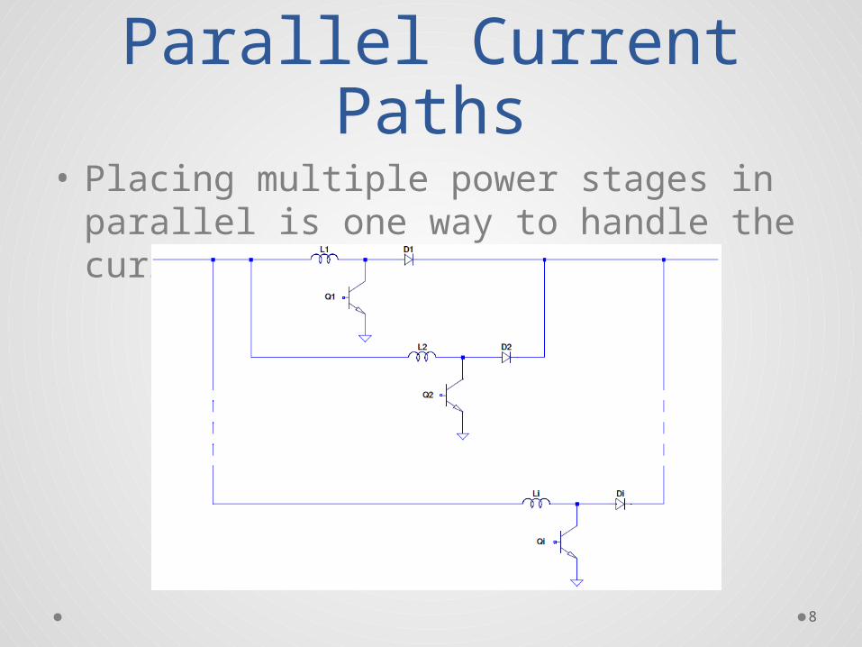
Parallel Current Paths• Placing multiple power stages in
parallel is one way to handle the current.

9
Parallel Paths (cont.)• Again, the inductors caused
problems.
• 8 inductors were required• An integrated circuit controller
solution was found.
10
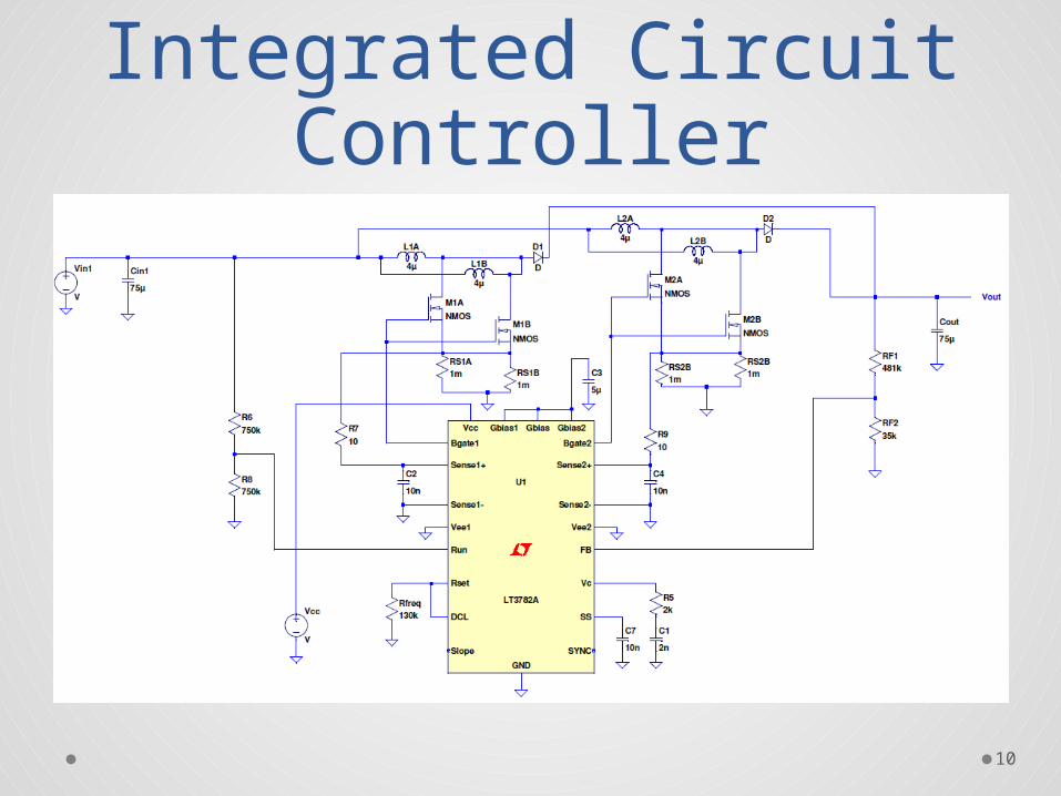
Integrated Circuit Controller
11
PCB Implementation• Some of the paths shown in the
previous diagram would have currents of 100 A.
• The cost of a PCB capable of handling these currents may be cost prohibitive.

12
Boost Power-Stage Platform
• High-current sections of a boost converter placed on separate platform, connected by cables.
• Current and voltage sensor output to microcontroller.
• Gate switching would determined by microcontroller, sent through gate drive circuit.

13
Boost Power-Stage Platform (cont.)

14
Flyback Specifications• High current caused for multiple design
alterations.• 4:7 turns ratio• Voltage Primary 8V-40V. Secondary Voltage 14V.• 16.7% to 50% Duty cycle• Current max 5A in 14.3A• Inductance on primary 20μH

Flyback Schematic

16
Flyback Transformer• Selection of core geometry and material.• Toroid, E I core with gap• Kool mμ, ferromagnetic material, MPP• Core loss due to eddy currents and hysteresis ,
where k,m and n are constants that pertain to specific core material, is frequency and is the maximum flux density.

17
𝐵𝑀𝑎𝑥• Core saturation• Residual flux• Gauss• Units used for B and H
are not consistant

18
Litz Wire• High frequency
increases wire loss due to skin effect.
• Multistrand Litz wire distributes current
• Small wire gauge allows signal to penetrate into the wire.
• Higher cost• Window fill

• Measure impedance at different frequencies• Different sources and loads have different
electrochemical characteristics that can change overtime
• Humidity, temperature, oxidation & electrode corrosion
• Diffusion creates impedance at low frequencies (Warburg) makes impedance difficult to determine
• Electron & ion transport, gas & solid phase reactant transport, heterogeneous reactions different characteristic time-constants exhibited at different AC frequencies.
EIS Testing

EIS Setup• The device under test (DUT) will be the
battery, PV panel and ultra-capacitor.
Block diagram required for FRA to preform tests and obtain data.

FRA & eLoad• FRA injects a range of
frequencies along with a perturbation into the test device & signals the programmable load
• Measures voltage and current; creates Bode and Nyquist Plots
• Programmable eLoad varies impedance throughout the test.
Programmable eLoad
Frequency Response Analyzer (FRA)

EIS Setup Phases• FRA Computer
interfaceo Manuals, Drivers, XP OS
• FRA out signalo Frequency sweep test
• Cooling T connectoro Battery, ultra-capacitors,
PV panel
• C2E2 EIS testing setupo Battery & ultra-capacitors
FRA Computer interface
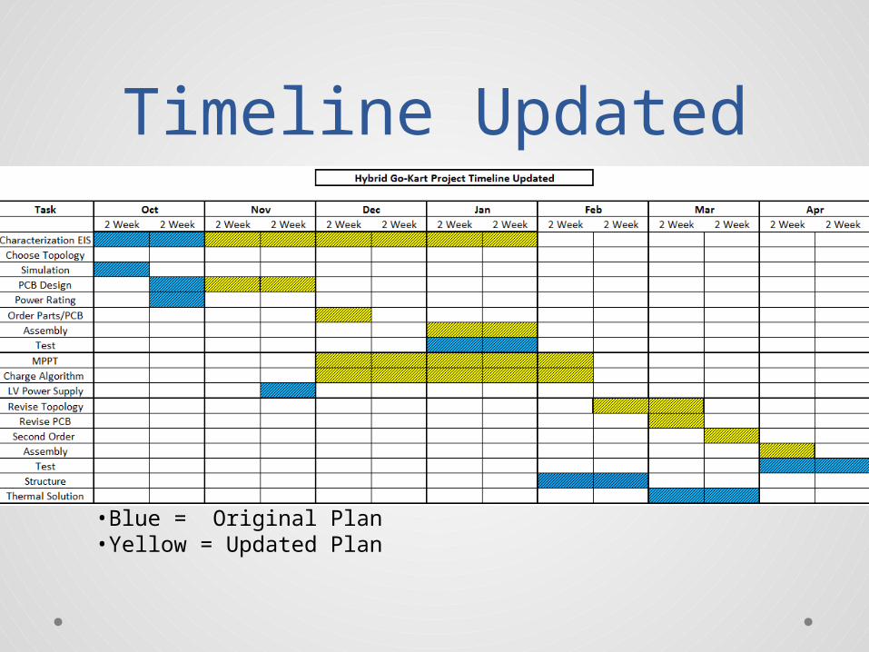
Timeline Updated
•Blue = Original Plan•Yellow = Updated Plan

24
Next Steps• PCB Design of Flyback and Gate Drivers
• Physical Layout of Boost Power-Stage Platform
• EIS of Battery and Ultra-Capacitors
• Software algorithm and MPPT

25
Questions?