high speed printed circuit board design - universiteit … · -reduction of crosstalk and radiation...
TRANSCRIPT
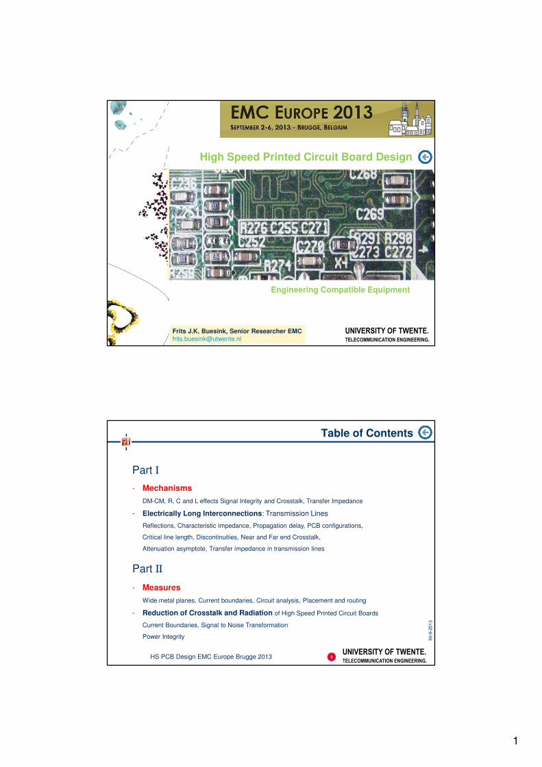
1
Frits J.K. Buesink, Senior Researcher [email protected]
Picture or Drawing 20.7 x 8.6 cm
UNIVERSITY OF TWENTE.
TELECOMMUNICATION ENGINEERING.
High Speed Printed Circuit Board Design
Engineering Compatible Equipment
UNIVERSITY OF TWENTE.
TELECOMMUNICATION ENGINEERING.
Table of Contents
2HS PCB Design EMC Europe Brugge 2013
- Mechanisms
DM-CM, R, C and L effects Signal Integrity and Crosstalk, Transfer Impedance
- Electrically Long Interconnections: Transmission Lines
Reflections, Characteristic impedance, Propagation delay, PCB configurations,
Critical line length, Discontinuities, Near and Far end Crosstalk,
Attenuation asymptote, Transfer impedance in transmission lines
- Measures
Wide metal planes, Current boundaries, Circuit analysis, Placement and routing
- Reduction of Crosstalk and Radiation of High Speed Printed Circuit Boards
Current Boundaries, Signal to Noise Transformation
Power Integrity
Part Ι
Part ΙΙ

2
UNIVERSITY OF TWENTE.
TELECOMMUNICATION ENGINEERING.
Table of Contents
3HS PCB Design EMC Europe Brugge 2013
- Mechanisms
DM-CM, R, C and L effects Signal Integrity and Crosstalk, Transfer Impedance
- Electrically Long Interconnections: Transmission Lines
Reflections, Characteristic impedance, Propagation delay, PCB configurations,
Critical line length, Discontinuities, Near and Far end Crosstalk,
Attenuation asymptote, Transfer impedance in transmission lines
Part Ι
UNIVERSITY OF TWENTE.
TELECOMMUNICATION ENGINEERING.
Elementary Electromagnetic Principles
a. What about currents?
4HS PCB Design EMC Europe Brugge 2013
I1 I2
I3213 III +=
Kirchhoff’s Electrical Current Law
Ia Ib
Every current must
have a return path!ba Ι=Ι
when applied to one conductor…

3
UNIVERSITY OF TWENTE.
TELECOMMUNICATION ENGINEERING.
Interconnections: Common Mode Current “Leaks Out”
every current has a return path! where does your (return) current flow?
5HS PCB Design EMC Europe Brugge 2013
Source Load
“Ground”
Icm
“Common-mode” current
“Differential-mode” currentIdm
UNIVERSITY OF TWENTE.
TELECOMMUNICATION ENGINEERING.
Interconnections: Common Mode Current “Leaks Out”
the path of the common-mode current could be a second, comparable circuit
6HS PCB Design EMC Europe Brugge 2013
Source Load
Icm“Common-mode” current
“Differential-mode” currentIdm
Several mechanisms are possible:
• Resistive
• Capacitive
• Inductive
4
UNIVERSITY OF TWENTE.
TELECOMMUNICATION ENGINEERING.
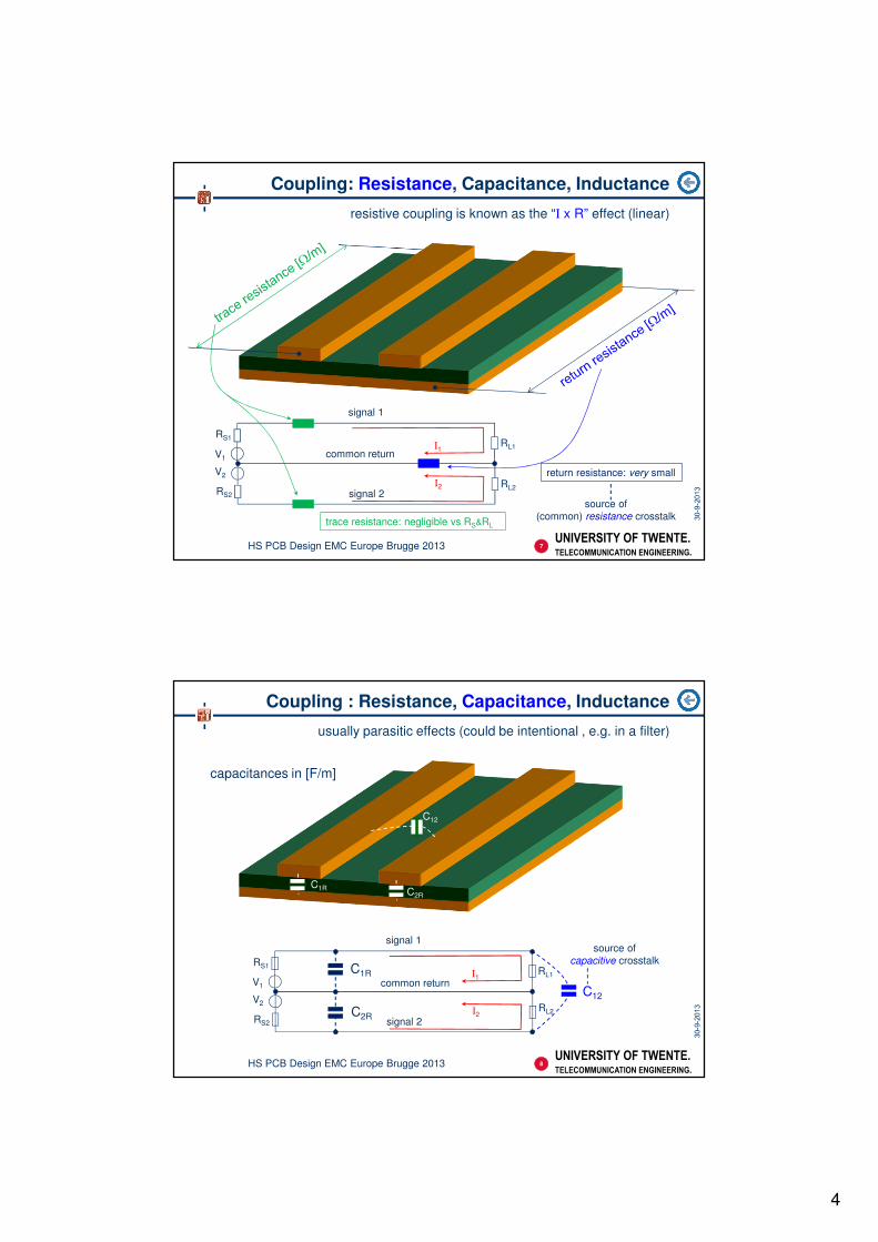
Coupling: Resistance, Capacitance, Inductance
resistive coupling is known as the “Ι x R” effect (linear)
7HS PCB Design EMC Europe Brugge 2013
signal 1
common return
signal 2
V1
V2
RS1
RS2
RL1
RL2
trace resistance: negligible vs RS&RL
return resistance: very small
Ι1
Ι2
source of
(common) resistance crosstalk
UNIVERSITY OF TWENTE.
TELECOMMUNICATION ENGINEERING.
Coupling : Resistance, Capacitance, Inductance
usually parasitic effects (could be intentional , e.g. in a filter)
8HS PCB Design EMC Europe Brugge 2013
signal 1
common return
signal 2
V1
V2
RS1
RS2
RL1
RL2
Ι1
Ι2
source of
capacitive crosstalk
C12
C1R
C2R
C1R C2R
C12
capacitances in [F/m]

5
UNIVERSITY OF TWENTE.
TELECOMMUNICATION ENGINEERING.
Coupling : Resistance, Capacitance, Inductance
usually parasitic effects (could be intentional)
9HS PCB Design EMC Europe Brugge 2013
signal 1
common return
signal 2
V1
V2
RS1
RS2
RL1
RL2
Ι1
Ι2
source of
inductive crosstalk
M12
L1 L2
M12
inductances in [H/m]
L1
L2
Lreturn
k=
Coupling Coefficient
UNIVERSITY OF TWENTE.
TELECOMMUNICATION ENGINEERING.
Inductive EMI Effects
Every current is accompanied by a magnetic field (conditio sine qua non)
10HS PCB Design EMC Europe Brugge 2013
H = Magnetic Field [A/m] - H
Magnetic Flux Density:
B = µ.H
= current towards reader
Legend
= current into paper
original current conductor return current conductor

6
UNIVERSITY OF TWENTE.
TELECOMMUNICATION ENGINEERING.
Combined Magnetic Field Pattern (Moiré Effect)
two radial line patterns model the actual magnetic field pattern
11HS PCB Design EMC Europe Brugge 2013
Conductors collocate:
complete cancellation
Conductors close:
complex patterns
UNIVERSITY OF TWENTE.
TELECOMMUNICATION ENGINEERING.
Elementary Electromagnetic Principles
What about voltages? Faraday’s and Lenz’ Law
12HS PCB Design EMC Europe Brugge 2013
Kirchhoff’s Voltage Law
Us
R1
R2
UR1
UR
2
021 =++ RRS UUU
Faraday’s Law:
?
The minus sign indicates that the induced
voltage, when shorted, would produce a
current with a magnetic field opposing the
original field direction!
This effect is referred to as Lenz’ Law

7
UNIVERSITY OF TWENTE.
TELECOMMUNICATION ENGINEERING.
Elementary Electromagnetic Principles
magnetic field changes induce voltages in conductor loops (self-inductance)
13HS PCB Design EMC Europe Brugge 2013
loop 1flux Φ
( )2
2
1iLE ⋅⋅=Energy contained in Magnetic Field: [Joule]
UNIVERSITY OF TWENTE.
TELECOMMUNICATION ENGINEERING.
A Wire Loop on a PCB Groundplane
to demonstrate the effect of changes in looparea
14HS PCB Design EMC Europe Brugge 2013
8
UNIVERSITY OF TWENTE.
TELECOMMUNICATION ENGINEERING.
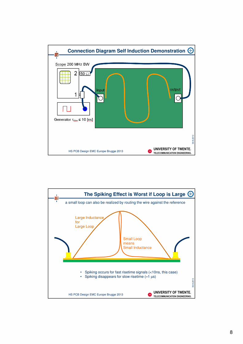
Connection Diagram Self Induction Demonstration
15HS PCB Design EMC Europe Brugge 2013
UNIVERSITY OF TWENTE.
TELECOMMUNICATION ENGINEERING.
The Spiking Effect is Worst if Loop is Large
a small loop can also be realized by routing the wire against the reference
16HS PCB Design EMC Europe Brugge 2013
Large Inductance
for
Large Loop
Small Loop
means
Small Inductance
• Spiking occurs for fast risetime signals (<10ns, this case)
• Spiking disappears for slow risetime (≈1 µs)

9
UNIVERSITY OF TWENTE.
TELECOMMUNICATION ENGINEERING.
Time Domain Response of Self Induction Board
spike on channel 1 shows time needed to build up magnetic field
17HS PCB Design EMC Europe Brugge 2013
Channel 1
Channel 2
UNIVERSITY OF TWENTE.
TELECOMMUNICATION ENGINEERING.
Frequency Domain Response of Self Induction Board
high frequencies are attenuated if the loop is made larger
18HS PCB Design EMC Europe Brugge 2013

10
UNIVERSITY OF TWENTE.
TELECOMMUNICATION ENGINEERING.
Setting up the Spectrum Analyzer (SA) for Transfer
19HS PCB Design EMC Europe Brugge 2013
UNIVERSITY OF TWENTE.
TELECOMMUNICATION ENGINEERING.
SA “Transfer” Measurement 1 MHz – 1 GHz
20HS PCB Design EMC Europe Brugge 2013

11
UNIVERSITY OF TWENTE.
TELECOMMUNICATION ENGINEERING.
Better Performance with Foil on Top
21HS PCB Design EMC Europe Brugge 2013
UNIVERSITY OF TWENTE.
TELECOMMUNICATION ENGINEERING.
Wide ground planes also show: the Skin Effect
related effect of Lenz’Law and the basis for shielding absorption
22HS PCB Design EMC Europe Brugge 2013
Ι
Current
Source
0 dInduced Eddy currents oppose
direction of external current
(Lenz’ Law)Sheet metal
Ed
dy c
urr
en
ts
curr
ent
density
0 d
J0
δ
e
J0
δ
d
d eJJ−
⋅= 0
12
UNIVERSITY OF TWENTE.
TELECOMMUNICATION ENGINEERING.
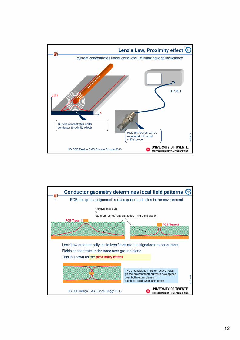
Lenz’s Law, Proximity effect
current concentrates under conductor, minimizing loop inductance
23HS PCB Design EMC Europe Brugge 2013
Ι
Current concentrates under
conductor (proximity effect)
R=50Ω
Field distribution can be
measured with small
sniffer probe
x
J(x)
UNIVERSITY OF TWENTE.
TELECOMMUNICATION ENGINEERING.
Conductor geometry determines local field patterns
PCB designer assignment: reduce generated fields in the environment
24HS PCB Design EMC Europe Brugge 2013
Lenz’Law automatically minimizes fields around signal/return conductors:
Fields concentrate under trace over ground plane.
This is known as the proximity effect
PCB Trace 1
PCB Trace 2
Relative field level
or
return current density distribution in ground plane
Two groundplanes further reduce fields
(in the environment) currents now spread
over both return planes (!)
see also: slide 22 on skin effect

13
UNIVERSITY OF TWENTE.
TELECOMMUNICATION ENGINEERING.
Return Current Distribution Magnitude in Ground Plane
lowering the trace reduces volume “filled with flux”
25HS PCB Design EMC Europe Brugge 2013
H
D
J0 or Φ0 JD or ΦD
2
001
1
+
≈Φ
Φ=
H
DJ
J DDSource:
Johnson, H
“High-Speed
Digital Design”
1993
UNIVERSITY OF TWENTE.
TELECOMMUNICATION ENGINEERING.
Skin Effect, Proximity Effect, Induction
Two messages
26HS PCB Design EMC Europe Brugge 2013
1. Keep all signal lines close to their return conductors
on a PCB this choice is made at design time!
2. Make return conductors as wide as possible (A-Symmetric)and, if possible enclose the signal line in the return
(coax, not so easy on a Printed Circuit Board)
compromise: use 2 wide return conductors above and below (strip-line)
Symmetric: ws = wr
ws
wr
ws
A-Symmetric: ws<< wr
wr

14
UNIVERSITY OF TWENTE.
TELECOMMUNICATION ENGINEERING.
Lenz’ Law: the Board
PCB traces with different widths and return paths
27HS PCB Design EMC Europe Brugge 2013
UNIVERSITY OF TWENTE.
TELECOMMUNICATION ENGINEERING.
Lenz’ Law PCB: the Schematic Diagram
seven PCB traces with different widths and return paths
28HS PCB Design EMC Europe Brugge 2013
6. Trace on Ground Plane
7. Trace on Ground Plane with adjacent “Guard Traces”
Ground Via
5. Trace on Edge of Ground Plane
4. Thin Long Trace (big ‘loop’far from ground trace)
3. Wide ‘Meandering’ Trace (big loop, far from ground plane)
2. Thin Short Trace (big loop, far from ground plane)
1. Wide Short Trace (big loop, far from ground plane)
Sq
ua
re-w
ave
Ge
ne
rato
r
Effects shown previously form the basis for this set of experiments
50
Te
rmin
ate
with
50
Ωlo
ad
scope
hop
inputs
15
UNIVERSITY OF TWENTE.
TELECOMMUNICATION ENGINEERING.
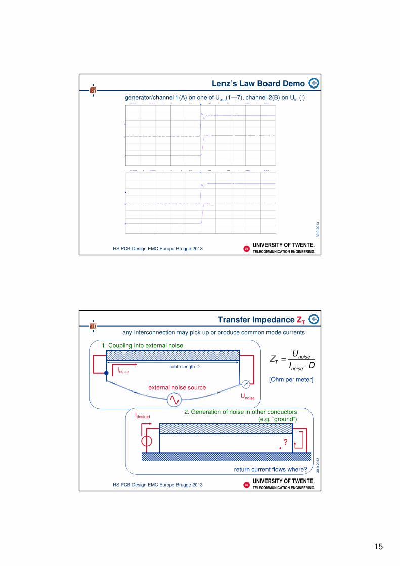
Lenz’s Law Board Demo
generator/channel 1(A) on one of Uout(1—7), channel 2(B) on Uin (!)
29HS PCB Design EMC Europe Brugge 2013
UNIVERSITY OF TWENTE.
TELECOMMUNICATION ENGINEERING.
Transfer Impedance ZT
any interconnection may pick up or produce common mode currents
30HS PCB Design EMC Europe Brugge 2013
external noise source
Inoise
Unoise
1. Coupling into external noise
cable length D
Idesired
return current flows where?
?
2. Generation of noise in other conductors
(e.g. “ground”)
DI
UZ
noise
noiseT
⋅=
[Ohm per meter]

16
UNIVERSITY OF TWENTE.
TELECOMMUNICATION ENGINEERING.
Coupling of Circuit Loops: Mutual induction
field loop 1 induces voltage in loop 2: crosstalk, transformer, reduction of ZT
31HS PCB Design EMC Europe Brugge 2013
I1
loop 1
loop 2
MModel:
flux Φ11
2
12
loop
loop
IM
Φ=
1
11
IL
Φ=
UNIVERSITY OF TWENTE.
TELECOMMUNICATION ENGINEERING.
Transformer Principle with a Printed Circuit Board
bottom line: a PCB can act as a (CM) noise source into the outside world
32HS PCB Design EMC Europe Brugge 2013
Coupled Flux
trace
ground plane = return conductor
Bottom Line: a Printed Circuit Board has Transfer-Impedance!
ΙCM

17
UNIVERSITY OF TWENTE.
TELECOMMUNICATION ENGINEERING.
Mechanism of the transfer impedance
common-mode current flows in return impedance, M reduces ZT
33HS PCB Design EMC Europe Brugge 2013
Ιcm
RS LS
L1
R0
Uin
Cable
Vin
MS1
cmSMjU Ι⋅⋅= 1ω
( )Scmin LjRU ω+Ι= ( )( )1SSScmin MLjRU −+Ι= ω
Transfer Inductance (LT)
1
S
UNIVERSITY OF TWENTE.
TELECOMMUNICATION ENGINEERING.
Demonstration of Transfer Impedance
uses several cables to demonstrate the effects
34HS PCB Design EMC Europe Brugge 2013

18
UNIVERSITY OF TWENTE.
TELECOMMUNICATION ENGINEERING.
Transfer Impedance Demo Schematic Diagram
generator loaded with 1 ohm and cable shield
35HS PCB Design EMC Europe Brugge 2013
Generator Analyzer
(50 Ω in)
51
51
51
ZT = 1 Ωis -34 dB
(conversion to dBΩ)
UNIVERSITY OF TWENTE.
TELECOMMUNICATION ENGINEERING.
Measured Impedances for UTP & Coax with/without Pig Tail
36HS PCB Design EMC Europe Brugge 2013
0 dBΩ line

19
UNIVERSITY OF TWENTE.
TELECOMMUNICATION ENGINEERING.
Cable ZT Assessment on Measurement Receiver
37HS PCB Design EMC Europe Brugge 2013
UNIVERSITY OF TWENTE.
TELECOMMUNICATION ENGINEERING.
Trace Separation over Groundplane is Important
once a wide metal plane is used for flux reduction
38HS PCB Design EMC Europe Brugge 2013
H
D
Current distribution of Ιsource over ground plane is
measure of flux density, Φ, coupling into cable:
at source ~L, at victim ~M!
source
sourcesourceL
Ι
Φ≈
source
victim
victim
sourceMΙ
Φ≈
proximity effect
closer line
“catches” more flux

20
UNIVERSITY OF TWENTE.
TELECOMMUNICATION ENGINEERING.HS PCB Design EMC Europe Brugge 2013
Mutual induction in practice
crosstalk created by mutual induction between two loops
source (50Ω)
scope
“ground” litz wire
single wire (source)
single wire (passive)
Only a change in current produces crosstalk!
39
50 Ω
dt
dIVnoise ~
B
50
Ω
A
Note that a slower rise time
produces less or no crosstalk at all!
UNIVERSITY OF TWENTE.
TELECOMMUNICATION ENGINEERING.
Ground Plane
Wide ground plane is preferred
return path for current!
HS PCB Design EMC Europe Brugge 2013
Mutual induction in practice
noise greatly reduced with wide return conductor (ground plane)
source (50Ω)
scope
single wire (source)
single wire (passive)
40
50 Ω
B
50
Ω
A
Icm “squeezes”
under cable
(proximity
effect)
21
UNIVERSITY OF TWENTE.
TELECOMMUNICATION ENGINEERING.
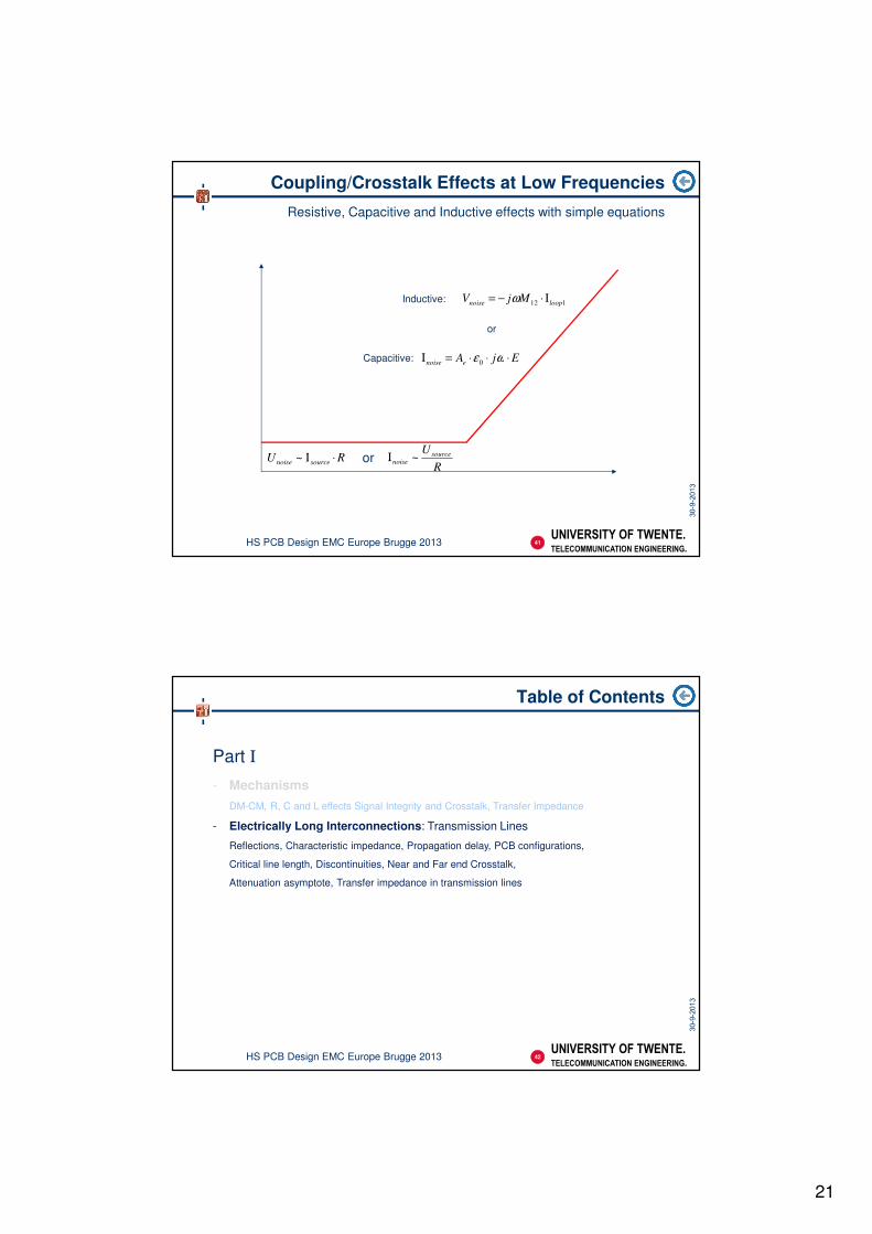
Coupling/Crosstalk Effects at Low Frequencies
Resistive, Capacitive and Inductive effects with simple equations
41HS PCB Design EMC Europe Brugge 2013
RU sourcenoise ⋅Ι~
or
orR
U sourcenoise ~Ι
112 loopnoise MjV Ι⋅−= ω
EjAenoise ⋅⋅⋅=Ι ωε 0
Inductive:
Capacitive:
UNIVERSITY OF TWENTE.
TELECOMMUNICATION ENGINEERING.
Table of Contents
42HS PCB Design EMC Europe Brugge 2013
- Mechanisms
DM-CM, R, C and L effects Signal Integrity and Crosstalk, Transfer Impedance
- Electrically Long Interconnections: Transmission Lines
Reflections, Characteristic impedance, Propagation delay, PCB configurations,
Critical line length, Discontinuities, Near and Far end Crosstalk,
Attenuation asymptote, Transfer impedance in transmission lines
Part Ι

22
UNIVERSITY OF TWENTE.
TELECOMMUNICATION ENGINEERING.
What Frequency is High and what is a Low Frequency?
wavelength or rise time is the key in comparison to interconnection length
43HS PCB Design EMC Europe Brugge 2013
“Small” ≤ 10% of Critical size
Analog world:
Critical size = half wavelength fmax [m]
Digital world:
Critical size = length of the rising edge [m]
τpd = X [ns/m] prop. delay
τr = Y [ns]
][msizeCriticalpd
r
τ
τ=
Achievement of EMC is easier on “small” systems (low frequencies)
UNIVERSITY OF TWENTE.
TELECOMMUNICATION ENGINEERING.
Combined Effects Above the Critical Frequency
example: crosstalk between two 3 [m] parallel lines
44HS PCB Design EMC Europe Brugge 2013
1 103
× 1 104
× 1 105
× 1 106
× 1 107
× 1 108
× 1 109
×
100−
80−
60−
40−
20−
0
Frequency [Hz]
Cro
ssta
lk [
dB
]
Resistive Effects “Transmission line” Effects
InductiveEffects
Capacitive
Critical Frequency
“Low Frequency”
Approach Acceptable

23
UNIVERSITY OF TWENTE.
TELECOMMUNICATION ENGINEERING.
Charactristic Impedance and Propagation Delay
a function of “per unit length” (PUL) parameters
45HS PCB Design EMC Europe Brugge 2013
speed νννν
L/2
L/2
Cv(t) i(t) v(t+δδδδt)i(t+δδδδt)
δδδδx
[ ]Ω==C
LZ
ti
tv0
)(
)(Characteristic Impedance
Ratio
⋅==
m
nsCLPD
ντ
1Propagation Delay
Z0
Loss Free transmission line
ZSZL
VS
UNIVERSITY OF TWENTE.
TELECOMMUNICATION ENGINEERING.
Transmission Lines and Signal Integrity
when properly terminated, only delay remains; otherwise: reflections occur
46HS PCB Design EMC Europe Brugge 2013
RS
(50
Ω)RL
(50 Ω)
So
urc
e
Lo
ad
VS
Coax Cable (50 Ω)
2SV
time delay
A
B
Scope Picture
B
A
SV
Without RL:
Reflections!

24
UNIVERSITY OF TWENTE.
TELECOMMUNICATION ENGINEERING.
Long interconnections: transmission lines
terminated in characteristic impedance
47HS PCB Design EMC Europe Brugge 2013
50
Ω
coax cable
Waveform for fast edge
stable impedance over length
A B
A
B
Using a cable,
appropriate for the job,
transient effects disappear
propagation delay remains
3 m RG58
UNIVERSITY OF TWENTE.
TELECOMMUNICATION ENGINEERING.
Long interconnections: transmission lines
if electrically “long” measures are needed to avoid reflections
48HS PCB Design EMC Europe Brugge 2013
A
coax cable
Waveform for fast edge
cable without termination
B
A
B
Long cable (50Ω line)
without termination:
reflections!
25
UNIVERSITY OF TWENTE.
TELECOMMUNICATION ENGINEERING.
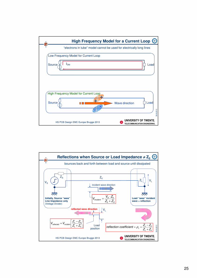
High Frequency Model for a Current Loop
“electrons in tube” model cannot be used for electrically long lines
49HS PCB Design EMC Europe Brugge 2013
Source Load
Low Frequency Model for Current Loop
Source Load
High Frequency Model for Current Loop
++
--
Wave direction
ΙDM
UNIVERSITY OF TWENTE.
TELECOMMUNICATION ENGINEERING.
Reflections when Source or Load Impedance ≠≠≠≠ Z0
bounces back and forth between load and source until dissipated
50HS PCB Design EMC Europe Brugge 2013
S
SIncident
ZZ
ZVV
+
⋅=
0
0
incident wave direction
0
0
ZZ
ZZtcoefficienreflection
L
LL
+
−== ρ
VLreflected wave direction
+
−=
0
0
ZZ
ZZVV
L
Lincidentreflected Load
position
Z0ZS
ZLVS
VL
Initially, Source “sees”Line Impedance only(Voltage Divider)
Load “sees” incidentwave + reflection
26
UNIVERSITY OF TWENTE.
TELECOMMUNICATION ENGINEERING.
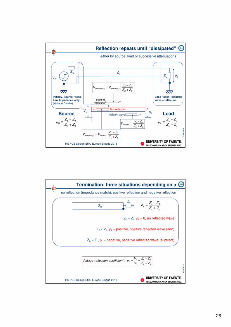
Reflection repeats until “dissipated”
either by source, load or successive attenuations
51HS PCB Design EMC Europe Brugge 2013
0
0
ZZ
ZZ
L
LL
+
−=ρ
0
0
ZZ
ZZ
S
SS
+
−=ρ
first reflection
+
−=
0
0)1(
ZZ
ZZVV
L
Lincidentreflected
second
reflection
+
−=
0
0)1()2(
ZZ
ZZVV
S
Sreflectedreflected
incident wave
S
SIncident
ZZ
ZVV
+
⋅=
0
0
VS VL
Z0ZS
ZLVS
VL
Initially, Source “sees”Line Impedance only(Voltage Divider)
Load “sees” incidentwave + reflection
LoadSource
UNIVERSITY OF TWENTE.
TELECOMMUNICATION ENGINEERING.
Termination: three situations depending on ρρρρ
no reflection (impedance match), positive reflection and negative reflection
52HS PCB Design EMC Europe Brugge 2013
Z0
ZL
0
0
ZZ
ZZ
L
LL
+
−=ρ
Z0 = ZL, ρL = 0, no reflected wave
Z0 < ZL, ρL = positive, positive reflected wave (add)
Z0 > ZL, ρL = negative, negative reflected wave (subtract)
0
0:ZZ
ZZ
V
VtcoefficienreflectionVoltage
L
L
i
rV
+
−==ρ

27
UNIVERSITY OF TWENTE.
TELECOMMUNICATION ENGINEERING.
Time Domain Reflectometry
fast oscilloscope + fast generator allow analysis of interconnection
53HS PCB Design EMC Europe Brugge 2013
Fast rise time
pulse generator
integrated
fast scope
interconnections
under test
Sa
mp
ling
He
ad
50 Ω
line
UNIVERSITY OF TWENTE.
TELECOMMUNICATION ENGINEERING.
Measurement of shielded twisted pair (STP) line
using Time Domain Reflectometry
54HS PCB Design EMC Europe Brugge 2013
time
ρ
1
-1
0-0.2
0.76
ρ
0 V
2.5 V2 V
4.4 V
5 V
50 Ω
input
reflection
scope display
convers
ions
ρ
Z=
∙ 0
Z0 = 50 Ω
Z= 50∙
A
A
“33 Ω”
“open”
“shorted”
3.5 m “33 Ω”
shielded twisted pair
1 m 50 W coax
1 m coax
3.5 m STP
33 Ω
oror
sw
itch

28
UNIVERSITY OF TWENTE.
TELECOMMUNICATION ENGINEERING.
ZS = 50 [Ω]
Z0 = 33 [Ω]
ZL = ∞ [Ω]
Vg= 5V (t ≥ 0)
Propagationdelay: T
The Lattice Diagram
simple tool / approach to show the effects of repeated reflections
55HS PCB Design EMC Europe Brugge 2013
t = 0:
t = T:
t = 2T:
t = 4T:
t = 3T:
ρ
= 0.2 ρ
= 1
2.0 V
2.0 + 2.0 + 0.4 =
= 4.4 V
4.4 + 0.4 + 0.08 =
= 4.88 V
2.0 + 2.0=
= 4.0 V
4.0 + 0.4 + 0.4=
= 4.8 VZ0
ZSZL
VS VL
Vg
Source: VS Load: VL
= Vg
= 2.0
time
VS
2T 4T0
UNIVERSITY OF TWENTE.
TELECOMMUNICATION ENGINEERING.
Transmission Lines on Printed Circuit Boards
micro striplines, striplines and asymmetric dual striplines
56HS PCB Design EMC Europe Brugge 2013
Micro-Stripline Stripline
PCB Lecher line
(only possible for one trace)
Signal
Return
Asymmetric
Dual Stripline
Buried
Micro-Stripline
d
b
t
wS
wR
εr
general dimensions
b = dielectric heightd = height over ground planet = copper thicknesswS= Trace WidthwR= Ground Plane Widthεεεεr = relative dielectric constant
order of magnitude
Z0 = 30 - 100 [ΩΩΩΩ]ττττpd = 5 - 10 [ns/m]
29
UNIVERSITY OF TWENTE.
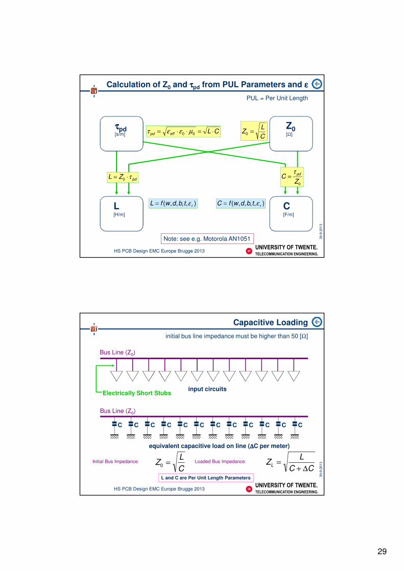
TELECOMMUNICATION ENGINEERING.
Calculation of Z0 and ττττpd from PUL Parameters and εεεε
PUL = Per Unit Length
57HS PCB Design EMC Europe Brugge 2013
ττττpd[s/m]
Z0[Ω]
L[H/m]
C[F/m]
CLeffpd ⋅=⋅⋅= 00 µεετC
LZ =0
0ZC
pdτ=
pdZL τ⋅= 0
),,,,( rtbdwfL ε= ),,,,( rtbdwfC ε=
Note: see e.g. Motorola AN1051
UNIVERSITY OF TWENTE.
TELECOMMUNICATION ENGINEERING.
Capacitive Loading
initial bus line impedance must be higher than 50 [Ω]
58HS PCB Design EMC Europe Brugge 2013
input circuits
Bus Line (Z0)
C C C C C C C C C C C
equivalent capacitive load on line (∆∆∆∆C per meter)
C
Bus Line (Z0)
Initial Bus Impedance:
C
LZ =0
Loaded Bus Impedance:
CC
LZL
∆+=
L and C are Per Unit Length Parameters
Electrically Short Stubs

30
UNIVERSITY OF TWENTE.
TELECOMMUNICATION ENGINEERING.
What Makes a Transmission Line Long?
determined by wavelength of highest frequency in the transported signal
59HS PCB Design EMC Europe Brugge 2013
A
50%
90%
10%
τh
τr
Fknee
hτπ ⋅
1
rτπ ⋅
1
rτ⋅2
1
F1 F2
am
plit
ude
log (frequency)
f
1~
2
1~
f
Signal on Digital Board:
A Trapezoid in the Time DomainCharacterized by:Rise or Fall Time: ττττr
Pulse Duration: ττττh
Fknee source:
Johnson, H
“High-Speed
Digital Design”
1993
UNIVERSITY OF TWENTE.
TELECOMMUNICATION ENGINEERING.
Critical Line Length: Analog and Digital Worlds
half wavelength of Fknee equals length of leading edge
60HS PCB Design EMC Europe Brugge 2013
[ ]mX2
λ=
X
Analog World
[ ]mXpd
r
τ
τ=
Digital World
[ ]mF pd
r
r
pdkneeFknee
τ
τ
ττ
υλ=
⋅⋅⋅
=⋅
=
2
12
1
22
=
s
m
pdτυ
1
propagationspeed:
[ ]1
2
1 −
⋅= sF
r
kneeτ

31
UNIVERSITY OF TWENTE.
TELECOMMUNICATION ENGINEERING.
A Line is Long if FKNEE approaches FCross-Over
FCO is a property (related to length) of the the actual line
61HS PCB Design EMC Europe Brugge 2013
FCross-Over or FCO is related to actual Line Length
One “Half Wavelength” of FCO fits the line (or cable) length
FCO is also called the “Critical Frequency”
Fknee
hτπ ⋅
1
rτπ ⋅
1
rτ⋅2
1
F1 F2
am
plit
ude
log (frequency)
Fknee is related to Signal Rise (or Fall) Time
Sig
na
l P
rop
ert
y: F
KN
EE
Ph
ysic
al L
ine
Pro
pe
rty: F
CO
UNIVERSITY OF TWENTE.
TELECOMMUNICATION ENGINEERING.
Comparison of some Logic Families
knee frequencies and corresponding critical lengths
62HS PCB Design EMC Europe Brugge 2013
Logic Family Rise Time
[s]
Knee Frequency
[MHz]
Critical length
in FR4 [m] )*
“Low Frequency” (Crit./6) [m]
4000 CMOS 10-6 0.5 143 24
HCMOS 10-8 50 1.43 0.24
LVCMOS 3x10⁻⁹ 167 0.43 0.07
AHCMOS 10-9 500 0.143 0.02
Note: Lines over this Length need “Transmission Line Treatment”
)* Using Strip Line Propagation Delay: τpd = 7 [ns/m]
Advice: Choose the Slowest Acceptable Logic Family if there is a Choice!
FKneelcrit=
λ
=
ν

32
UNIVERSITY OF TWENTE.
TELECOMMUNICATION ENGINEERING.
Transfer Impedance of a PCB Interconnection
all interconnections have it, PCB traces are no exception!
63HS PCB Design EMC Europe Brugge 2013
D
UZ
cm
noiseT
⋅Ι=
+-
Ιcm
Unoise
Das receiver….
as source…. Ιdm
Udm
Ιnoise
UNIVERSITY OF TWENTE.
TELECOMMUNICATION ENGINEERING.
Printed Circuit Board has transfer impedance
Either susceptible or emitting! Connected cabling acts as antennae
64HS PCB Design EMC Europe Brugge 2013
“Twin-wires”
traces over ground trace or plane = two conductor interconnections!
reduced fields and noise
antenna
antenna
Vnoise Vnoise
AS = 0 0 < AS < 1

33
UNIVERSITY OF TWENTE.
TELECOMMUNICATION ENGINEERING.
Avoid “Long Stubs” route a “Daisy Chain”!
certainly no branches longer than the critical length
65HS PCB Design EMC Europe Brugge 2013
Instead of this…
Try this…
output /driver
input/load
input/loadinput/load
input +termination
Use high-currentdriver when
located mid-line
UNIVERSITY OF TWENTE.
TELECOMMUNICATION ENGINEERING.
Discontinuities in the Signal Trace
Impedance change and branches
66HS PCB Design EMC Europe Brugge 2013

34
UNIVERSITY OF TWENTE.
TELECOMMUNICATION ENGINEERING.
Measurements on Discontinuities Board (1)
top line 1 almost 50 Ohms
67HS PCB Design EMC Europe Brugge 2013
50 Ω
ρ
UNIVERSITY OF TWENTE.
TELECOMMUNICATION ENGINEERING.
Measurements on Discontinuities Board (2)
line 2: 100 Ohms
68HS PCB Design EMC Europe Brugge 2013
50 Ω
ρ
100 Ω
ρ
ρ
−
+⋅=1
150Znote:

35
UNIVERSITY OF TWENTE.
TELECOMMUNICATION ENGINEERING.
Measurements on Discontinuities Board (3)
line 3: partly 65, partly 117 Ohms
69HS PCB Design EMC Europe Brugge 2013
65 Ω
ρ
117 Ω
ρ
ρ
−
+⋅=1
150Znote:
UNIVERSITY OF TWENTE.
TELECOMMUNICATION ENGINEERING.
Measurements on Discontinuities Board (4)
line 4: impedance decreases as lines dissect; multiple reflections
70HS PCB Design EMC Europe Brugge 2013
50 Ω
ρ
100 Ω
ρ
ρ
−
+⋅=1
150Znote:
first side-track (drop to 59 Ω)
second side-track (to 46 Ω)

36
UNIVERSITY OF TWENTE.
TELECOMMUNICATION ENGINEERING.
Discontinuities (Video)
71HS PCB Design EMC Europe Brugge 2013
UNIVERSITY OF TWENTE.
TELECOMMUNICATION ENGINEERING.
Vias in Signal Traces
return current needs a path too: if not available, it will find one elsewhere!
72HS PCB Design EMC Europe Brugge 2013
Signal traceReference 1
Reference 2
Reference 2
Reference 3
?
?
A
B
C
Signal trace

37
UNIVERSITY OF TWENTE.
TELECOMMUNICATION ENGINEERING.
Provide a return current path when “changing layers”
shoot ground-via in close proximity (existing well within critical length O.K.)
73HS PCB Design EMC Europe Brugge 2013
Signal traceReference 1
Reference 2
Reference 2
Reference 3
A
B
C
Signal trace
The Ground Viaprovides a Pathfor the Return Current
UNIVERSITY OF TWENTE.
TELECOMMUNICATION ENGINEERING.
Discontinuities in the Return Current Path
ground plane interruptions
74HS PCB Design EMC Europe Brugge 2013

38
UNIVERSITY OF TWENTE.
TELECOMMUNICATION ENGINEERING.
Measurements on the Ground Slot Board (1)
Track 1, wide slot; unaided—with ground trace—with capacitively coupled ground trace
75HS PCB Design EMC Europe Brugge 2013
50 Ω
ρ
100 Ω
ρ
ρ
−
+⋅=1
150Znote:
UNIVERSITY OF TWENTE.
TELECOMMUNICATION ENGINEERING.
Wide Ground Slot (Video)
76HS PCB Design EMC Europe Brugge 2013

39
UNIVERSITY OF TWENTE.
TELECOMMUNICATION ENGINEERING.
Measurements on the Ground Slot Board (2)
Track 2, 1.8 mm slot; unaided—covered with metal plate
77HS PCB Design EMC Europe Brugge 2013
50 Ω
ρ
90 Ω
ρ
ρ
−
+⋅=1
150Znote:
59 mm 1.8 mm
UNIVERSITY OF TWENTE.
TELECOMMUNICATION ENGINEERING.
Narrow Ground Slot (Video)
78HS PCB Design EMC Europe Brugge 2013

40
UNIVERSITY OF TWENTE.
TELECOMMUNICATION ENGINEERING.
Crosstalk when Risetime << Line Propagation Delay
effects occur at the current location of the transition
79HS PCB Design EMC Europe Brugge 2013
Capacitive
iC (forward)iC (backward)
Near end Far end
Inductive
M
i
iL (backward)
Near end Far end
iC (forward) - iL (backward)iC (backward) + iL (backward)
Propagation
Direction
UNIVERSITY OF TWENTE.
TELECOMMUNICATION ENGINEERING.
Influence of Propagation Delay on Shape of Crosstalk
“Far End” goes with Incident Wave, “Near End” returns for two line delays
80HS PCB Design EMC Europe Brugge 2013
Near end Far end
t = 0
t = T = l. τpd
“now”
t = 2T =2 l. τpd
≈ rise time
tim
e
distance0 l
Source: Johnson, H.W. et. al. “High-Speed Digital Design”, Prentice Hall,New Jersey, 1993
Far end:
signal edge
and crosstalk
arrive together
Near end:
Crosstalk
spreads out
over time
41
UNIVERSITY OF TWENTE.
TELECOMMUNICATION ENGINEERING.
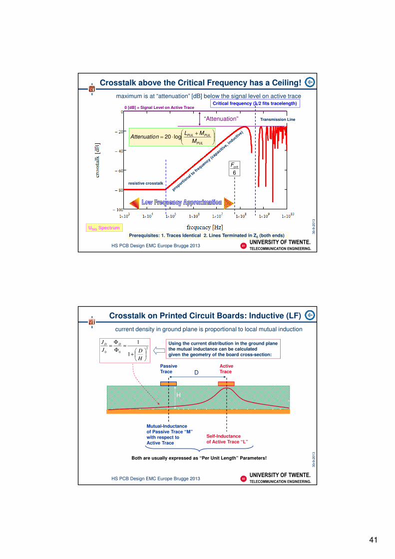
Crosstalk above the Critical Frequency has a Ceiling!
maximum is at “attenuation” [dB] below the signal level on active trace
81HS PCB Design EMC Europe Brugge 2013
Critical frequency (λλλλ/2 fits tracelength)
Transmission Line
resistive crosstalk
0 [dB] = Signal Level on Active Trace
“Attenuation”
+⋅=
PUL
PULPUL
M
MLnAttenuatio log20
Prerequisites: 1. Traces Identical 2. Lines Terminated in Z0 (both ends)
USIG Spectrum
6critF
UNIVERSITY OF TWENTE.
TELECOMMUNICATION ENGINEERING.
Crosstalk on Printed Circuit Boards: Inductive (LF)
2
001
1
+
≈Φ
Φ=
H
DJ
J DD
82HS PCB Design EMC Europe Brugge 2013
current density in ground plane is proportional to local mutual induction
ActiveTrace
PassiveTrace
Self-Inductanceof Active Trace “L”
Mutual-Inductanceof Passive Trace “M”with respect toActive Trace
Both are usually expressed as “Per Unit Length” Parameters!
D
H
Using the current distribution in the ground planethe mutual inductance can be calculatedgiven the geometry of the board cross-section:

42
UNIVERSITY OF TWENTE.
TELECOMMUNICATION ENGINEERING.
Combination of capacitive and inductive crosstalk
depending on load of source line, capacitive or inductive effects dominate
83HS PCB Design EMC Europe Brugge 2013
50 Ω instrument
or termination
50 Ω instrument
or termination
50 Ω generator
50 Ω lines
Termination
select switch
H
E Z0
active line
passive line
(Source) (Load)
Original Source:
J.J. Goedbloed
“EMC”, Kluwer 1993
Passive Line
Active Line
Near End Far End
UNIVERSITY OF TWENTE.
TELECOMMUNICATION ENGINEERING.
Crosstalk on PCB Demonstration (Proto)
Board with active trace and “20” and “30” [dB] Passive traces
84HS PCB Design EMC Europe Brugge 2013
ActiveTrace
-20 [dB]Trace
-30 [dB]Trace
Tracelengths: active 430 [mm]
-20 [dB] 430 [mm]
-30 [dB] 430 [mm]
FR4: εr = 4.7 εeff = 3.75

43
UNIVERSITY OF TWENTE.
TELECOMMUNICATION ENGINEERING.
Crosstalk PCB with “20 & 30 [dB] Attenuation” Lines
three micro stripline traces, total length each: 43 [cm]
85HS PCB Design EMC Europe Brugge 2013
εr = 4.7
2.7 [mm] 2.7 [mm] 2.7 [mm]
6 [mm] 2 [mm]
1.6 [mm]
-30
[d
B]
Pa
ssiv
e tra
ce
-20
[d
B]
Pa
ssiv
e tra
ce
Active
tra
ce
Trace Impedances: 50 [ΩΩΩΩ]
Propagation Delay: 5.2 [ns/m]
Trace Inductance: 264 [nH/m]
Trace Capacitance: 103 [pF/m]
Effective Dielectric Constant: εεεεr = 3.75
Trace ParametersSeparation 2 [mm] 6 [mm]
Mutual Inductance [nH/m] 27 9
Mutual Capacitance [pF/m] 11 3.4
IEEE Trans. on EMC Vol. 55 No. 4 Aug. 2013
“Overview of Signal Integrity and EMC Design Technologies on PCB”
UNIVERSITY OF TWENTE.
TELECOMMUNICATION ENGINEERING.
Crosstalk Measurement Results for Test PCB
all traces terminated. note: most analysers have a linear frequency scale
86HS PCB Design EMC Europe Brugge 2013
“20 [dB]” Trace
“30 [dB]” Trace
20 [dB] Attenuation Trace
-70
-60
-50
-40
-30
-20
-10
0
1.00E+06 2.01E+08 4.01E+08 6.01E+08 8.01E+08 1.00E+09 1.20E+09
linear frequency scale
20 [dB] Attenuation Trace
-70
-60
-50
-40
-30
-20
-10
0
1.00E+06 1.00E+07 1.00E+08 1.00E+09
logarithmic frequency scale
174 [MHz]
44
UNIVERSITY OF TWENTE.
TELECOMMUNICATION ENGINEERING.
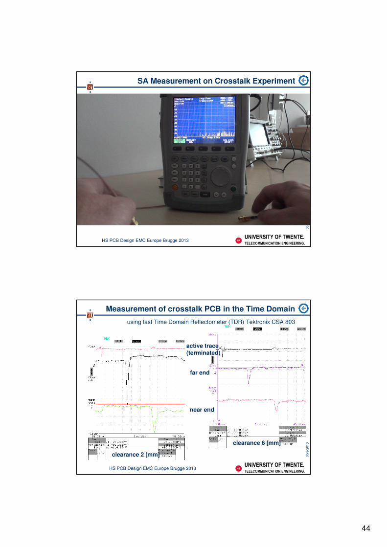
SA Measurement on Crosstalk Experiment
87HS PCB Design EMC Europe Brugge 2013
UNIVERSITY OF TWENTE.
TELECOMMUNICATION ENGINEERING.
Measurement of crosstalk PCB in the Time Domain
using fast Time Domain Reflectometer (TDR) Tektronix CSA 803
88HS PCB Design EMC Europe Brugge 2013
active trace(terminated)
far end
near end
clearance 2 [mm]
clearance 6 [mm]

45
UNIVERSITY OF TWENTE.
TELECOMMUNICATION ENGINEERING.
Summary of Effects
designable parameters: asymmetry and line length
89HS PCB Design EMC Europe Brugge 2013
line length
Shorter LineLonger Line
- Att
line geometry
moreasymmetry
lessasymmetry
log(frequency)
cro
ssta
lk[d
B]
0
(attenuation)
Longer Line:LF and MF
crosstalk increases
UNIVERSITY OF TWENTE.
TELECOMMUNICATION ENGINEERING.
The End of Part ΙΙΙΙ
90HS PCB Design EMC Europe Brugge 2013
1. H.W.Johnson, M. Graham “High Speed Digital Design, A Handbook of
Black Magic” Prentice Hall, 1993, ISBN 0-13-395724-1
2. J.J. Goedbloed, “EMC”, Prentice Hall, 1992, ISBN 0-13-249293-8
3. H.W. Ott “EMC Engineering”, Wiley, 2009, ISBN 978-0-470-18930-6
6. F.J.K.Buesink “Printed Circuit Boards for the Education aimed at
Understandig Electromagnetic Effects”, User manual, University of
Twente, 2009http://www.utwente.nl/ewi/te/education/emc_demonstration_boards/Understandingelectro
magnetic_Effects_using_PCB_demos.pdf
7. IEEE “EMC Education Manual”, 1992http://www.emcs.org/pdf/EMCman.pdf

46
UNIVERSITY OF TWENTE.
TELECOMMUNICATION ENGINEERING.
Table of Contents
91HS PCB Design EMC Europe Brugge 2013
- Measures
Wide metal planes, Current boundaries, Circuit analysis, Placement and routing
- Reduction of Crosstalk and Radiation of High Speed Printed Circuit Boards
Current Boundaries, Signal to Noise Transformation
Power Integrity
Part ΙΙ
UNIVERSITY OF TWENTE.
TELECOMMUNICATION ENGINEERING.
The Principle of the Current Boundary
a provision to split loops (and shut out noise sources)
92HS PCB Design EMC Europe Brugge 2013
“Ground 1” “Ground 2”
Icm (noise current)
loop closes through “ground”
“Ground 2”“Ground 1”Icm
loop closes through “ground”
Create one or more “inner-loops”Short
circuit(s)
reduce looparea
check
module 1
module 2
(Mains cord 1)
(Mains cord 2)(I/O cable 1-2)
Situation in practicedetector:
AM-radio

47
UNIVERSITY OF TWENTE.
TELECOMMUNICATION ENGINEERING.
The concept of a current boundary on a PCB (1)
concept model
93HS PCB Design EMC Europe Brugge 2013
Module A
groundplane
Module B
conceptual boundary
boundary
Signal
Return
(Plane)
ground(-plane)
Signal
Return
boundary
decouplingcapacitor
to common
power supply
UNIVERSITY OF TWENTE.
TELECOMMUNICATION ENGINEERING.
The concept of a current boundary on a PCB (2)
traditionally, PCB edge forms boundary: interface electronics resides there
94HS PCB Design EMC Europe Brugge 2013
B
A
Sig
nal
tow
ard
s A
Sig
nal
tow
ard
s B
Po
wer
Lin
e
= buffer (can be bidirectional)
deco
up
lin
g c
ap
acit
or
Improvement:
• No current can pass unattended from module 1 to module 2
• Sources and Sinks of DM current are placed on the boundary
• All DM signals are “processed/polished” at the boundary
Note: Power Line Decoupling at a
Current Boundary is Not Possible
when Power Planes are used!

48
UNIVERSITY OF TWENTE.
TELECOMMUNICATION ENGINEERING.
Equivalent of Cable System Current Boundaries on PCB’s
quasi active shielding using a ground plane
95HS PCB Design EMC Europe Brugge 2013
Instead of
Cable Categories
we now have
Trace categories!
note: power supply is decoupled with capacitance to ground plane (see slide 134)
UNIVERSITY OF TWENTE.
TELECOMMUNICATION ENGINEERING.
Difference between Analog and Digital Circuits
analog: differences in currents & frequencies; digital: all signals are similar
96HS PCB Design EMC Europe Brugge 2013
C OUT
D
C IN
P0P1
P2
P3
UP/DNGND
VCC
PRE EN
CLK
Q0
Q1Q2
Q3
D Q
Q
Q
PRE
PRE GND
Q
Clock
Board lay-out Analog Circuits
separate current loops
sort loops: largest dΙ/dt smallest
minimize “common impedance”
Board lay-out Synchronous Digital
separate data from clocks&strobes
data/address lines may crosstalk
keep clock and strobe lines “clean”

49
UNIVERSITY OF TWENTE.
TELECOMMUNICATION ENGINEERING.
The Current Return Path is Important!
just a ground symbol is not sufficient
97HS PCB Design EMC Europe Brugge 2013
“ ”Is not enough!
UNIVERSITY OF TWENTE.
TELECOMMUNICATION ENGINEERING.
Simple High Speed PCB Stackup
two copper layers, suitable for “home fabrication”
98HS PCB Design EMC Europe Brugge 2013
Component side = Ground Plane
Traces on 1.6 [mm] FR-4 board over ground plane
0
20
40
60
80
100
120
0 1 2 3 4 5 6
Trace Width [mm]
Tra
ce I
mp
ed
an
ce [
Oh
m]
drill out copperfor pins not connected
to ground
1.6 [mm]
Propagation Delay: 5.2 [ns/m](MicroStripLine)
Notes:
Use wire jumpers
for “impossible” connections
Impedance considerations only
needed for long lines!
(>> 0.1 x critical length)
Interference from environment may havehigher frequencies than thosegenerated on the board!

50
UNIVERSITY OF TWENTE.
TELECOMMUNICATION ENGINEERING.
Discontinuities in Transmission Lines
two solutions: end termination and series termination
99HS PCB Design EMC Europe Brugge 2013
End Termination:
Z0
GND
+ VDD
VME Bus(Both Ends)
330 Ω
470 Ω
R = Z0
(NoGo: HighDissipation)
R
R = Z0
CTerm ≈≈≈≈ (2∙FCO∙R)-1
RCTerm
make sure line is “constant impedance”(Strip Line or Micro Strip Line)Average Impedance ≈≈≈≈ 50 [ΩΩΩΩ]
open endZ0
GND
ZSSeries Termination:R ≈ |Z0 - ZS|
Only use this method for point to point interconnections
proper transition seriousringing
A. ResistiveLoad
B. CapacitiveCoupling
C. T
heven
inN
etw
ork
short with respect to critical length!
UNIVERSITY OF TWENTE.
TELECOMMUNICATION ENGINEERING.
Effect of End Termination on Transmission Line
Low impedance driver on high(er) impedance line
100HS PCB Design EMC Europe Brugge 2013
Propagation delay UTP: ττττPD = 4.8 [ns/m], i.e. for length len = 3 [m]: nslent PDprop 4.14=⋅= τ
3 m “Z0 = 120Ω” line
Sourc
e 5
0Ω
?“open” end
ρS = -0.41 ρL = 1
Vg = 5 V
T: 7 V(!)
0:
3.5 V
2T:
3.5+3.5-1.4 =
= 5.6 V
3T:
7 -1.4 -1.4 =
4.2 V

51
UNIVERSITY OF TWENTE.
TELECOMMUNICATION ENGINEERING.
Simulation with LTSPICE
101HS PCB Design EMC Europe Brugge 2013
UNIVERSITY OF TWENTE.
TELECOMMUNICATION ENGINEERING.
Effect of End Termination on Transmission Line
demonstration using 3 [m] unshielded twisted pair line of 120Ω
102HS PCB Design EMC Europe Brugge 2013
Propagation delay UTP: ττττPD = 4.8 [ns/m], i.e. for length len = 3 [m]: nslent PDprop 4.14=⋅= τ
[ ]pFtoZ
lenC PD
Term 1501200
≈⋅
=τ
λ
2
=
∙∙
≈35 MHz
3 m “Z0 = 120Ω” line
50
Ωsourc
e
RL
= 1
20 Ω
CTerm ≈ total line capacitance
0 =#$
#$
τ#%= #$ ∙ #$
#$ =τ
= 40pF/m
+,-. ≥1
2 ∙ 0 ∙
150 pF

52
UNIVERSITY OF TWENTE.
TELECOMMUNICATION ENGINEERING.
Table of Contents
103HS PCB Design EMC Europe Brugge 2013
- Measures
Wide metal planes, Current boundaries, Circuit analysis, Placement and routing
- Reduction of Crosstalk and Radiation of High Speed Printed Circuit Boards
Current Boundaries, Signal to Noise Transformation
Power Integrity
Part ΙΙ
UNIVERSITY OF TWENTE.
TELECOMMUNICATION ENGINEERING.
Practical example: Emissions from a PCB
dual sided board with “as much ground plane as possible”
104HS PCB Design EMC Europe Brugge 2013
Printed Circuit Board withwired connections on all sides
EMC limit violations up to 20 [dB]

53
UNIVERSITY OF TWENTE.
TELECOMMUNICATION ENGINEERING.
Same PCB, Ground Plane Apertures covered with Foil
now the system is within its emission limits!
105HS PCB Design EMC Europe Brugge 2013
No more limit violations!
UNIVERSITY OF TWENTE.
TELECOMMUNICATION ENGINEERING.
Method of Trace Separation on Printed Circuit Boards
reduce mutual induction by separation over ground plane or use skin effect
106HS PCB Design EMC Europe Brugge 2013
distance reduces coupling
Skin effect reduces coupling

54
UNIVERSITY OF TWENTE.
TELECOMMUNICATION ENGINEERING.
Power Supply Decoupling
close to fast circuits; propagation speeds are equal for signal and power!
107HS PCB Design EMC Europe Brugge 2013
Effective
Loop
Area AE
∆∆∆∆i
∆∆∆∆t
∆∆∆∆Vsupplyvoltagetolerance
t
VCi
∂
∂⋅=capacitor equation:
max
minV
tiC
∆
∆⋅∆=
decoupling capacitor
design goal:
C
PCB traces
PCB traces
bo
nd
ing
wir
es
bo
nd
ing
wir
es
Larger C’s have more Inductance!
UNIVERSITY OF TWENTE.
TELECOMMUNICATION ENGINEERING.
Capacitors have parasitic elements
equivalent circuit diagram and high-frequency behaviour
108HS PCB Design EMC Europe Brugge 2013
LWire
LWire
LInternal
C
RESR
log(frequency)
|ZC|
fresonance
RESR
Cω
1SUMLω

55
UNIVERSITY OF TWENTE.
TELECOMMUNICATION ENGINEERING.
Parasitic Elements can be Located on the Board!
keep PCB traces short, select smallest capacitor for the job (size & value)
109HS PCB Design EMC Europe Brugge 2013
UNIVERSITY OF TWENTE.
TELECOMMUNICATION ENGINEERING.
Same capacitor, different on board inductances
Resonances between 67 and 195 MHz
110HS PCB Design EMC Europe Brugge 2013

56
UNIVERSITY OF TWENTE.
TELECOMMUNICATION ENGINEERING.
Measuring Capacitors
111HS PCB Design EMC Europe Brugge 2013
UNIVERSITY OF TWENTE.
TELECOMMUNICATION ENGINEERING.112HS PCB Design EMC Europe Brugge 2013

57
UNIVERSITY OF TWENTE.
TELECOMMUNICATION ENGINEERING.
Frequencies > 500 MHz: Use Distributed Capacitance
instead of one capacitor use many smaller values, ultimately distributed
113HS PCB Design EMC Europe Brugge 2013
Comparison of decoupling with four different
and four identical capacitors (Source: Ott)
100n//10n//1n//100pF
4 x 100nF
due to propagation delay, only a limited
area capacitance is available (Source Ott)
UNIVERSITY OF TWENTE.
TELECOMMUNICATION ENGINEERING.
Power Plane Combination is a Transmission Line
“attenuation” is only 6 dB! cutting up one layer into smaller patches improve it
114HS PCB Design EMC Europe Brugge 2013
Symmetric Power Transmission Line
has large “transfer-impedance”(little noise reduction)
and large “slot-antenna” emission!
solid reference plane
“data” traces
Possible other layers
individual power “patches”
separate electronic modules
connected by “thin” traces
high εand/or
very thin!

58
UNIVERSITY OF TWENTE.
TELECOMMUNICATION ENGINEERING.
Power Planes or Power Traces?
noise on power planes is only attenuated by 6 dB
115HS PCB Design EMC Europe Brugge 2013
Maximum symmetry
e.g. Power Planes
Asymmetry
e.g. narrow Trace over wide Ground
SN
T
frequency
SN
T
frequency
>20 dB
Attenuation 6 dB
UNIVERSITY OF TWENTE.
TELECOMMUNICATION ENGINEERING.
Simultaneous Switching Causes GroundBounce
reason is the internal (bonding) wire inductance and high current spikes
116HS PCB Design EMC Europe Brugge 2013
Vcc
Cin Rin
Lout
LVcc
Lgnd
Icc
Iout
(smd) bypass C
Chip internal GND is lifted
from the Board GND.
Lgnd = bondwire inductance
59
UNIVERSITY OF TWENTE.
TELECOMMUNICATION ENGINEERING.
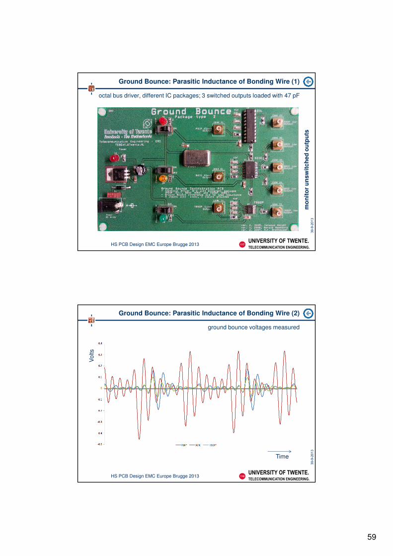
Ground Bounce: Parasitic Inductance of Bonding Wire (1)
octal bus driver, different IC packages; 3 switched outputs loaded with 47 pF
117HS PCB Design EMC Europe Brugge 2013
mo
nit
or
un
sw
itc
he
do
utp
uts
UNIVERSITY OF TWENTE.
TELECOMMUNICATION ENGINEERING.
Ground Bounce: Parasitic Inductance of Bonding Wire (2)
ground bounce voltages measured
118HS PCB Design EMC Europe Brugge 2013
Vo
lts
Time

60
UNIVERSITY OF TWENTE.
TELECOMMUNICATION ENGINEERING.
The Ground Lift Problem also Affects A/D Convertors
heavy load on digital outputs lifts (digital) ground: input offset created!
119HS PCB Design EMC Europe Brugge 2013
=
Vin
Analog
Input
Digital Output
Long Output Bus Lines
A/D
Converter
Re
ce
ivin
g C
ircu
its
?
Buffer reduces output loadA_GND D_GND
UNIVERSITY OF TWENTE.
TELECOMMUNICATION ENGINEERING.
Solution to PCB cable noise: add current boundary
separate “inside” (PCB) from “outside” (the world)
120HS PCB Design EMC Europe Brugge 2013
Ιcm
noise
short-circuit

61
UNIVERSITY OF TWENTE.
TELECOMMUNICATION ENGINEERING.
More Information
121HS PCB Design EMC Europe Brugge 2013
http://www.utwente.nl/ewi/te/education/
Understanding electromagnetic effects using PCB demos
High Speed PCB Design EMC Europe Brugge 2013
SigNoise
A book describing the PCB demos used
This presentation as a .pdf
Program to do calculations on PCB transmission lines
(does not run on Windows7; use Windows XP virtual PC)
UNIVERSITY OF TWENTE.
TELECOMMUNICATION ENGINEERING.
Literature
122HS PCB Design EMC Europe Brugge 2013
1. H.W.Johnson, M. Graham “High Speed Digital Design, A Handbook of
Black Magic” Prentice Hall, 1993, ISBN 0-13-395724-1
2. J.J. Goedbloed, “EMC”, Prentice Hall, 1992, ISBN 0-13-249293-8
3. H.W. Ott “EMC Engineering”, Wiley, 2009, ISBN 978-0-470-18930-6
4. F.B.J. Leferink “Reduction of Radiated Electromagnetic Fields
by Creation of Geometrical Asymmetry”, PhD Thesis, University of
Twente, 2001, ISBN 90-365-1689-7
5. F.B.J. Leferink “Power and Signal Integrity and Electromagnetic
Emission, the balancing act of decoupling, planes and tracks”, IEEE
EMC Symposium, Honolulu, 2007
6. F.J.K.Buesink “Printed Circuit Boards for the Education aimed at
Understandig Electromagnetic Effects”, User manual, University of
Twente, 2009http://www.utwente.nl/ewi/te/education/emc_demonstration_boards/Understandingelectrom
agnetic_Effects_using_PCB_demos.pdf
7. IEEE “EMC Education Manual”, 1992http://www.emcs.org/pdf/EMCman.pdf

62
UNIVERSITY OF TWENTE.
TELECOMMUNICATION ENGINEERING.
The End of Part ΙΙΙΙΙΙΙΙ
123HS PCB Design EMC Europe Brugge 2013