a practical guide to high-speed printed circuit board layout - wdv
TRANSCRIPT

Th W ld L d i Hi h P f Si l P i S l tiThe World Leader in High Performance Signal Processing Solutions
A Practical Guide to A Practical Guide to High-Speed Printed Circuit
Board LayoutBoard LayoutJohn Ardizzoni Dennis FallsAnalog Devices Avnet Electronics Marketing

Agendag
OverviewSchematicLocation, location, locationTrust no oneTrust no onePower supply bypassingParasiticsGround and power planes PackagingRF Signal routing and shieldingg g gChecking the layoutSummary
2

Overview
PCB layout is one of the last steps in the design process and y p g poften one of the most criticalHigh-speed circuit performance is heavily dependant on layoutyA high-performance design can be rendered useless due to a poor or sloppy layoutToday’s presentation will help:Today s presentation will help:
Improve the layout processEnsure expected circuit performance is achievedReduce design timeReduce design timeLower cost Lower stress for you and the PCB designer
3

Th W ld L d i Hi h P f Si l P i S l tiThe World Leader in High Performance Signal Processing Solutions
Schematic

Schematic
The strength of any structure (including PCB’s) is only as g y ( g ) ygood as the foundation on which it built upon!A good layout starts with a good Schematic!Schematic flow and contentSchematic flow and contentInclude as much information as you canWhat should you include?
5

Items to Include on a Schematic
NotesComponent tolerances and case sizesPart numbers (internal/external/alternative)Board stack upT t li t dTests or alignment proceduresPower dissipationControlled impedance and line matchingComponent de ratingComponent de-rating Thermal requirementsKeep outsMechanical considerationsMechanical considerationsCritical component placementWarning flagsWhat ever else you can think of!
6
y

Schematic
40 MHz
C10.1uF
U1
+5V
R6301
S1C4
2.2uF
+5V
40 MHz OSC Out
Must be right at op amp supply
pins
Put C4 and C7 on back of board right under the
power supply pin.
Run 40MHz traces on bottom
Place this cap right at pin 14 to digital ground
+
R3562 ADA4860-
1
-
+
R4210
C50.01uF
R5562
C2 C3
C60.01uF
C7
U2
VIN
VOUT
R250
R750
of the board ensure signal trace is the same length
40 MHz OSC Out
R11K
Linear Regulator
Temperature
-5V
SAT SAT C72.2uF
U3
U4D11N4148
Must be right at op amp supply
pins
+5V
50+5V
FREQUENCY ADJUST1.0 C2=C3, use these 2 capacitors to adjust the -3dB BW
D ti T bl
+
See critical component placement drawing for location
AD590
ADP667Temperature
Sensor+12V +5V
VOUT
Linear Regulator
-12V -5V
+ +
U5
8
D21N4148
C810uFCase size 1210
C90.01uF
C110.1uF
C1210uFCase size1210
C1310uf
C16
-5V
V
+5V
R81K
1K
Derating Table
R1
R2R3C1C2C3U1
U2
VALUE12345678
62mW 10mWITEM REF DES ACTUALRATING
++10ufCase size1210 C14
0.1uFC15
0.1uF
10uF Case size
1210
2.0 All Resistors in ohms unless noted otherwise.3.0 All capacitors in pF unless noted otherwise.
6 0 U1 SOIC-14 U2 SOT-23-6 U3 SOIC-8 U4 SOIC-80.062"
Signal 1 Analog Ground 1
Digital GroundPower plane
A l G d 2
BOARD STACK UP1.0 All resistors and capacitors are 0603 case size unless noted otherwise.
4.0 Run analog traces on Signal 1 layer, run digital traces on Signal 2 layer
NOTES:
5.0 Remove ground plane on all layers under the mounting pins of U2
7
6.0 U1 SOIC 14, U2 SOT 23 6, U3, SOIC 8, U4 SOIC 8 Analog Ground 2 Signal 2

Th W ld L d i Hi h P f Si l P i S l tiThe World Leader in High Performance Signal Processing Solutions
Location, location, location!

Location, Location, Location, ,
Just as in real estate location is everything!Just as in real estate location is everything!Input/output and power connections are typically defined…Everything else is undefined
Critical component placementSignal routingCircuit and component proximityCircuit and component proximity
9

Th W ld L d i Hi h P f Si l P i S l tiThe World Leader in High Performance Signal Processing Solutions
Trust No One

Trust No One
If you’re doing your own y g ylayout, that’s one thing.If you’re not ….
11

Trust No One
If you’re doing your own y g ylayout, that’s one thing.If you’re not ….
Don’t assume the CAD group isDon t assume the CAD group is going to read your mind and get it right!
12

Trust No One
If you’re doing your own y g ylayout, that’s one thing.If you’re not ….
Don’t assume the CAD group isDon t assume the CAD group is going to read your mind and get it right!In the end you’re responsible ffor making it work!
13

Trust No One
If you’re doing your own y g ylayout, that’s one thing.If you’re not ….
Don’t assume the CAD group isDon t assume the CAD group is going to read your mind and get it right!You’re responsible for making it work!
When working with the CAD Group
14

Trust No One
If you’re doing your own y g ylayout, that’s one thing.If you’re not ….
Don’t assume the CAD group isDon t assume the CAD group is going to read your mind and get it right!You’re responsible for making it work!
When working with the CAD Group
Make sure you and the designer are on the same page
15

Trust No One
If you’re doing your own y g ylayout, that’s one thing.If you’re not ….
Don’t assume the CAD group isDon t assume the CAD group is going to read your mind and get it right!You’re responsible for making it work!
When working with the CAD Group
Make sure you and the designer are on the same pageBrief circuit explanation
16

Trust No One
If you’re doing your own y g ylayout, that’s one thing.If you’re not ….
Don’t assume the CAD group isDon t assume the CAD group is going to read your mind and get it right!You’re responsible for making it work!
When working with the CAD Group
Make sure you and the designer are on the same pageBrief circuit explanationC iti l t l t
17
Critical component placement

Trust No One
If you’re doing your own layout, that’s one thing.If you’re not ….
Don’t assume the CAD group is going to read your mind and getgoing to read your mind and get it right!You’re responsible for making it work!
When working with the CAD Group
Make sure you and the designer are on the same pageare on the same pageBrief circuit explanationCritical component placementInput/Output connections
18
Input/Output connections

Trust No One
If you’re doing your own layout, th t’ thithat’s one thing.If you’re not ….
Don’t assume the CAD group is going to read your mind and get it g g y gright!You’re responsible for making it work!
When working with the CADWhen working with the CAD Group
Make sure you and the designer are on the same pageBrief circuit explanationBrief circuit explanationCritical component placementInput/Output connectionsBoard outline drawing and stack up
19

Trust No One
If you’re doing your own layout, that’s one thingthat’s one thing.If you’re not ….
Don’t assume the CAD group is going to read your mind and get it i ht!right!
You’re responsible for making it work!
When working with the CAD GroupMake sure you and the designer are on the same pageBrief circuit explanationCritical component placementp pInput/Output connectionsBoard outline, stack upTell them to call you if they have a question!
20
question!

Th W ld L d i Hi h P f Si l P i S l tiThe World Leader in High Performance Signal Processing Solutions
Power Supply Bypassing

Power Supply Bypassingpp y yp g
Bypassing is essential to yp ghigh speed circuit performance
22

Power Supply Bypassingpp y yp g
Bypassing is essential to yp ghigh speed circuit performanceCapacitors right at power p g psupply pins
23
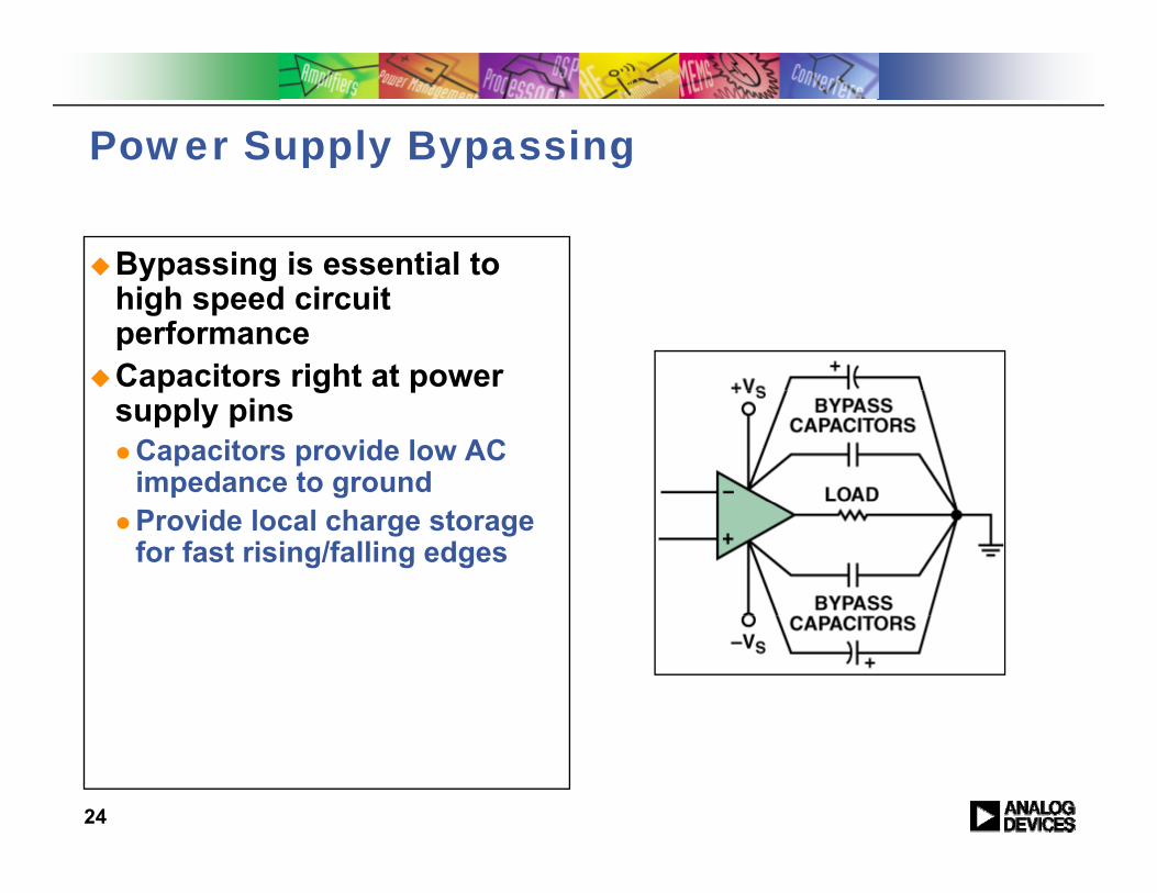
Power Supply Bypassingpp y yp g
Bypassing is essential to yp ghigh speed circuit performanceCapacitors right at power p g psupply pins
Capacitors provide low AC impedance to ground Provide local charge storage for fast rising/falling edges
24

Power Supply Bypassingpp y yp g
Bypassing is essential to yp ghigh speed circuit performanceCapacitors right at power
IC+VS
L1
1µHp g psupply pins
Capacitors provide low AC impedance to ground
C10.1µF
Provide local charge storage for fast rising/falling edges
Keep trace lengths shortEQUIVALENT DECOUPLED POWER LINE CIRCUIT RESONATES AT:
f =1
2π LC√
f = 500kHz
25
f = 500kHz

Power Supply Bypassingpp y yp g
Bypassing is essential to yp ghigh speed circuit performanceCapacitors right at power p g psupply pins
Capacitors provide low AC impedance to groundProvide local charge storage for fast rising/falling edges
Keep trace lengths short
26

Power Supply Bypassingpp y yp g
Bypassing is essential to yp ghigh speed circuit performanceCapacitors right at power p g psupply pins
Capacitors provide low AC impedance to groundProvide local charge storage for fast rising/falling edges
Keep trace lengths shortClose to load return
Helps minimize transient currents in the ground plane
27

Power Supply Bypassingpp y yp g
Bypassing is essential to high speed circuit performanceCapacitors right at power supply pinssupply pins
Capacitors provide low AC impedance to groundProvide local charge storage g gfor fast rising/falling edges
Keep trace lengths shortClose to load return
Helps minimize transient currents in the ground plane
ValuesIndividual circuit performance
28
Individual circuit performance

Power Supply Bypassingpp y yp g
Bypassing is essential to high speed circuit performanceCapacitors right at power supply pinssupply pins
Capacitors provide low AC impedance to groundProvide local charge storage for fast rising/falling edgesfast rising/falling edges
Keep trace lengths shortClose to load return
Helps minimize transient currentsHelps minimize transient currents in the ground plane
ValuesIndividual circuit performance
29
Maintains low AC impedance

Power Supply Bypassingpp y yp g
Bypassing is essential to high speed circuithigh speed circuit performanceCapacitors right at power supply pins
Capacitors provide low AC impedance to groundProvide local charge storage for fast rising/falling edges
Keep trace lengths shortKeep trace lengths shortClose to load return
Helps minimize transient currents in the ground plane
V lValuesIndividual circuit performanceMaintains low AC impedanceMultiple resonances
30
p

Power Supply Bypassingpp y yp g
Bypassing is essential to high d i it fspeed circuit performance
Capacitors right at power supply pins
Capacitors provide lowCapacitors provide low impedance AC return Provide local charge storage for fast rising/falling edges
Keep trace lengths shortKeep trace lengths shortClose to load return
Helps minimize transient currents in the ground plane
V lValuesIndividual circuit performanceMaintains low AC impedanceMultiple resonances
31
Multiple resonancesFerrite beads

Th W ld L d i Hi h P f Si l P i S l tiThe World Leader in High Performance Signal Processing Solutions
Parasitics

Parasitics
Parasite – An organism that grows, feeds, and is sheltered on g g , ,or in a different organism while contributing nothing to the survival of its host.
Parasitics in high-speed PCB’s, can destroy circuit performance!
33

Parasitics
PCB parasites take the form of undesired capacitors, inductors and resistors embedded within the PCBinductors and resistors embedded within the PCBParasitics are extremely difficult to remove from a PCBPrevention is the best method to minimize parasitics
34

Trace/Pad Capacitancep
dA
kAC =d
C3.11
K = relative dielectric constantK = relative dielectric constantA = area in cm2
d = spacing between plates in cm
35

Trace/Pad Capacitancep
dAExample: Pad of SOIC
L = 0.2cm W = 0.063cm
kA
K= 4.7
A = 0.0126cm2
dkAC3.11
=
K = relative dielectric constant
d = 0.073cm
C = 0.072pFK = relative dielectric constant
A = area in cm2
d = spacing between plates in cm
36

Trace/Pad Capacitancep
Example: Pad of SOIC
L = 0 2cm W = 0 063cm
dA
L = 0.2cm W = 0.063cm
K= 4.7
A = 0.0126cm2
kA
A 0.0126cm
d = 0.073cm
C = 0.072pF
dkAC3.11
=
K = relative dielectric constant C
p
K = relative dielectric constantA = area in cm2
d = spacing between plates in cm
Reduce Capacitance1) Increase board thickness or layers
2) Reduce trace/pad area 3) Remove ground plane
37

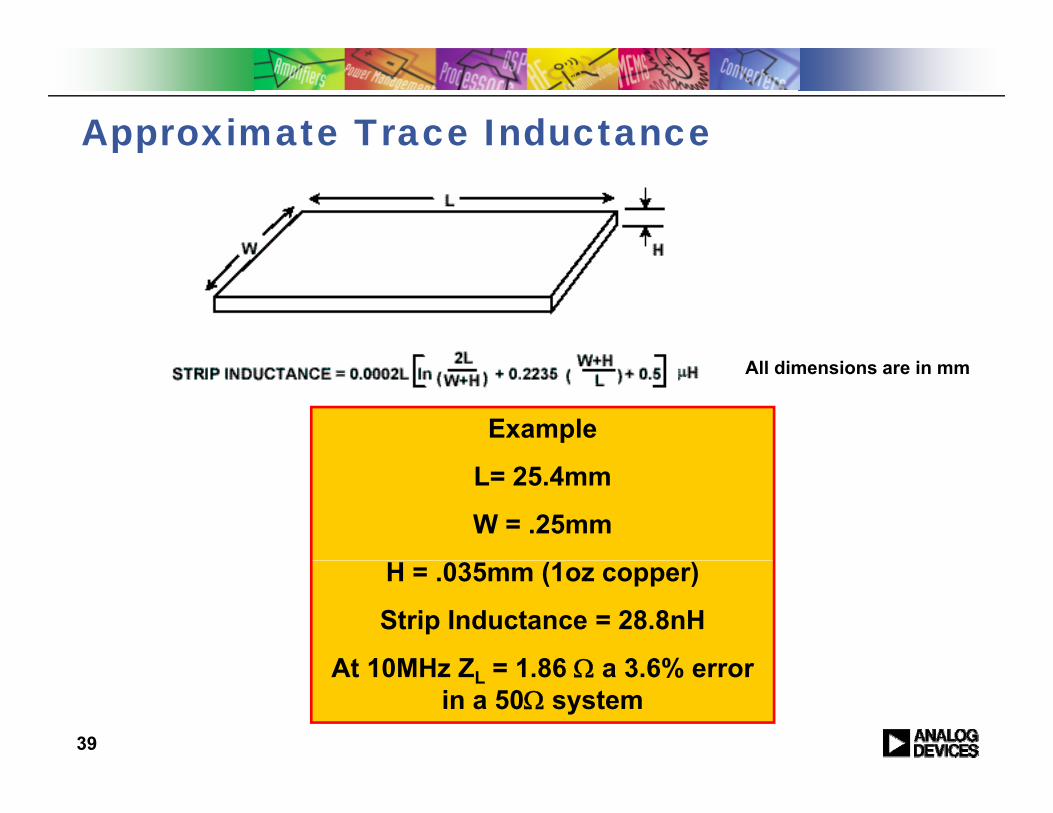
Approximate Trace Inductancepp
38
All dimensions are in mm
Approximate Trace Inductancepp
Example
All dimensions are in mm
L= 25.4mm
W = .25mm
H = .035mm (1oz copper)
Strip Inductance = 28.8nH
At 10MH Z 1 86 Ω a 3 6% error
39
At 10MHz ZL = 1.86 Ω a 3.6% error in a 50Ω system

Approximate Trace Inductancepp
Example
All dimensions are in mm
Minimize Inductance L= 2.54cm =25.4mm
W = .25mm1) Use Ground plane
2) Keep length short (halving the length reducesH = .035mm (1oz copper)
Strip Inductance = 28.8nH
At 10MH Z 1 86 Ω a 3 6% error
the length reduces inductance by 44%)
3) Doubling width only reduces inductance by
40
At 10MHz ZL = 1.86 Ω a 3.6% error in a 50Ω system
reduces inductance by 11%

Via Parasitics
Via Inductance Via Capacitance
⎤⎡ ⎞⎛ 4h 155.0 TDC r≈ε pF
L = inductance of the via, nHD2 = diameter of clearance hole in the ground plane, cmD di t f d di i
nH⎥⎦
⎤⎢⎣
⎡ +⎟⎠⎞
⎜⎝⎛≈ 14ln2
dhhL
12
1
DDC r
−≈ pF
H = length of via, cmD = diameter of via, cm
D1 = diameter of pad surrounding via, cmT = thickness of printed circuit board, cm
= relative electric permeability of circuit board materialC = parasitic via capacitance, pF
rε
Given:H= 0.157 cm thick board,D= 0.041 cm
C parasitic via capacitance, pF
Given:T = 0.157cm,D 0 071
L ~ 1.2nhD1=0.071cm D2 = 0.127
C ~ 0.51pf
41

Via Cross Section
D
T&H
D2
T&H
D
D1
D
42

Capacitor Parasitic Modelp
LRP RS
r
C
C = Capacitor
RDA CDA
RP = insulation resistance RS = equivalent series resistance (ESR)L = series inductance of the leads and plates RDA = dielectric absorption
43
RDA = dielectric absorptionCDA = dielectric absorption

Resistor Parasitic Model
C LCP L
RR = ResistorCP = Parallel capacitanceL= equivalent series inductance (ESL)
R
44
L= equivalent series inductance (ESL)

Low Frequency Op Amp Schematicq y p p
45

High Speed Op Ampg p p pSchematic
46

High Speed Op Ampg p p pSchematic
Parasitic Capacitance
47

48
http://www.analog.com/en/design-tools/dt-multisim-spice-program-download/design-center/index.html

Stray Capacitance Simulation Schematicy p
49

Frequency Response with 2pF Stray Capacitanceq y p p y p
1.8dB peaking
1.8dB peaking
1.8dB peaking
50

Stray Inductance y
Parasitic Inductance
51

Parasitic Inductance Simulation Schematic
AD8055 24.5mm x .25mm” =29nH
52

Pulse Response With and Without Ground pPlane
0.6dB overshoot
53

Transient Response AD8009p1GHz Current Feedback Amplifier
RF402Ω
+5V10uF
402ΩRG
0.1uF
150Ω0.1uF
10 F
-5V10uF
54

Small Changes Can Make a Big Difference!g g
55
Circuit BCircuit A

Improper Use of Scope Probe Ground Clipp p p p
56

Effect of Clip Lead Inductancep
57

Proper Grounding for Scope Probe in High-p g p gSpeed Measurments
58

Small Changes Make Big Differencesg gCircuit BCircuit A
21ns 17ns
59
25% reduction in ringing duration and amplitude

Th W ld L d i Hi h P f Si l P i S l tiThe World Leader in High Performance Signal Processing Solutions
Ground and Power Planes

Ground and Power Planes Provide
A common reference pointpShieldingLower noiseLower resistanceLower resistanceLower impedanceReduces parasiticsHeat sinkPower distribution
61

Ground Plane
II
I
62
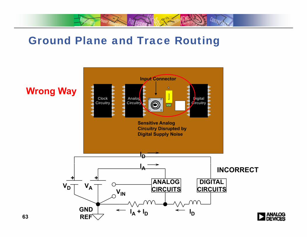
Ground Plane and Trace RoutingGround Plane and Trace Routing
DigitalCircuitry
AnalogCircuitry
Res
isto
r
ClockCircuitry
Wrong WayInput Connector
CircuitryCircuitryCircuitry
Sensitive Analog Circuitry Disrupted by Digital Supply NoiseDigital Supply Noise
ID
ANALOGCIRCUITS
DIGITALCIRCUITSVD VA
+ +
IA
VIN
INCORRECT
63IDIA + ID
VIN
GNDREF

Ground Plane and Trace RoutingGround Plane and Trace Routing
DigitalCircuitry
AnalogCircuitry
Res
isto
r
ClockCircuitry
Wrong WayCircuitryCircuitryCircuitry
Sensitive Analog Circuitry Disrupted by Digital Supply NoiseDigital Supply Noise
ID
ANALOGCIRCUITS
DIGITALCIRCUITSVD VA
+ +
IA
VIN
INCORRECT
64IDIA + ID
VIN
GNDREF

Ground Plane and Trace RoutingGround Plane and Trace Routing
DigitalCircuitry
AnalogCircuitry
Res
isto
r
Right WayCircuitry
ClockCircuitry
Sensitive Analog Circuitry Safe from Digital Supply Noise
IDIA CORRECT
ANALOGCIRCUITS
DIGITALCIRCUITSVD VA
+ +
VIN
65ID
IAGNDREF

Ground Plane and Trace RoutingGround Plane and Trace Routing
DigitalCircuitry
AnalogCircuitry
Res
isto
r
Right WayCircuitry
ClockCircuitry
Sensitive Analog Circuitry Safe from Digital Supply Noise
IDIA CORRECT
ANALOGCIRCUITS
DIGITALCIRCUITSVD VA
+ +
VIN
66ID
IAGNDREF

Ground Plane and Trace RoutingGround Plane and Trace Routing
Grounding Example:
Top layer is solid ground.
Res
isto
r
Signal Input Termination p y g
Bottom has a trace/transmission line connecting the RF connector to the load. R t t fl i th t l
Top Side
Resistor
Return current flows in the top layer ground plane directly above the trace on the opposite side.
Bottom side
67

Ground Plane and Trace Routing
Grounding Example: DC Current vs. AC Current:
AC current follows the
path of least impedance
Ground Plane and Trace Routing
In a split or broken ground, the return currents follow the path of least i d
Res
isto
r
DC currentimpedanceAt DC, the current follows the path of least resistance As the frequency increases the
DC current follows the
path of least resistance
As the frequency increases, the current follows the path of least inductanceSince there is now a ‘loop’ the inductance can be quite high and the circuit can now propagate EMI/RFI
68

Grounding Mixed Signal ICs: Single PC Boardg g g
ANALOG DIGITAL
VA VD
MIXEDVA VDANALOGCIRCUITS
DIGITALCIRCUITS
AGND DGND
SIGNALDEVICE
SYSTEMSTAR
GROUNDA A D D
ANALOGGROUND PLANE
DIGITALGROUND PLANE
GROUND
DA
DIGITALANALOG
69
SUPPLYSUPPLY

Ground Plane Recommendations
There is no single grounding method which is guaranteed to work 100% of the time!R d l d t d itiRemove ground plane under op amps to reduce parasitic capacitanceAt least one layer on each PC board MUST be dedicated to ground plane!pProvide as much ground plane as possible especially under traces that operate at high frequencyUse thickest metal as feasible (reduces resistance and provides improved thermal transfer)improved thermal transfer)Use multiple vias to connect same ground planes togetherDo initial layout with split analog and digital ground planesFollow recommendations on device data sheet (read datasheet)Follow recommendations on device data sheet (read datasheet)Keep bypass capacitors and load returns close to reduce distortionConnect analog, digital and RF grounds at one point
70

Th W ld L d i Hi h P f Si l P i S l tiThe World Leader in High Performance Signal Processing Solutions
Packaging and Pinout

Op Amp Packaging and Pinoutp p g g
Packaging plays a large role in high-speed applicationsg g p y g g p ppSmaller packages
Better at higher speedsLess parasiticsLess parasiticsCompact layout
Analog Devices Low Distortion PinoutAnalog Devices Low Distortion PinoutIntuitively makes more sense Compact layoutStreamline signal flowStreamline signal flowLower distortion
72

Op Amp SOIC Packagingp p g g
Traditional SOIC-8 layoutFeedback routed around or underneath amplifierp
73

Op Amp SOIC Packagingp p g g
Traditional SOIC-8 layoutFeedback routed around or underneath amplifierp
74

Analog Devices Low Distortion Pinoutg
Pinout enables compact Original Pin-Outplayout Disable FB 1
2
3
8
7
6
–IN
+IN
+VS
V+
-
NC
3
4
6
5–VS
+IN VOUT
NC
SOIC
1 8NC +VS
SOIC
2
5
6
7FEEDBACK–IN+IN
S
OUTPUTNC–VS
3
4
14-0
-001
75
0481
LFCSP

Analog Devices Low Distortion Pinoutg
Pinout enables compact Original Pin-OutplayoutLower distortion
Disable FB 1
2
3
8
7
6
–IN
+IN
+VS
V+
-
3
4
6
5–VS
+IN VOUT
NC
SOIC
1 8NC +VS
SOIC
2
5
6
7FEEDBACK–IN+IN
S
OUTPUTNC–VS
3
4
4-0-
001
76
0481
LFCSP

Analog Devices Low Distortion Pinoutg
Pinout enables compact Original Pin-OutplayoutLower distortionImproved thermal
Disable FB 1
2
3
8
7
6
–IN
+IN
+VS
V+
-
Improved thermal performance
3
4
6
5–VS
+IN VOUT
NC
SOIC
1 8NC +VS
SOIC
2
5
6
7FEEDBACK–IN+IN
S
OUTPUTNC–VS
3
4
4-0-
001
77
0481
LFCSP

Analog Devices Low Distortion Pinoutg
Pinout enables compact Original Pin-OutplayoutLower distortionImproved thermal
Disable FB 1
2
3
8
7
6
–IN
+IN
+VS
V+
-
Improved thermal performanceLFCSP
AD8099 AD8045 AD8000
3
4
6
5–VS
+IN VOUT
NC
SOICAD8099, AD8045, AD8000, ADA4899, ADA4857, ADA4817
1 8NC +VS
SOIC
2
5
6
7FEEDBACK–IN+IN
S
OUTPUTNC–VS
3
4
4-0-
001
78
0481
LFCSP

Low distortion pinout enables compact p pand streamline layout
79

Low distortion pinout enable compact and p pstreamline layout
Tantalum
C
RF
C
RL
AD
80XX
RT
RG R
00
Tantalum
80

Th W ld L d i Hi h P f Si l P i S l tiThe World Leader in High Performance Signal Processing Solutions
RF Signal Routing and Shielding

In This Section
RF Components from Analog DevicesPC Board Circuit Material Types and Minimizing Lossesyp gMicrostrip and Stripline Transmission Lines Ground Plane Layout ConsiderationsDeveloping a RF Printed Circuit BoardDeveloping a RF Printed Circuit Board Using Discrete Components with RF DevicesShielding of RF Circuit Boards
82

RF Components from Analog Devices
http://www.analog.com/en/rfif-components/products/index.html
83
p g p p

Analog Devices Components Requiring Matched RF Interfaces
AD60x, AD8xxx and ADL533x series of RF/IF and Variable Gain AmplifiersADF70xx and 702x series Radio Transmitters and TransceiversAD4xxx and ADF7xxx series of PLL Synthesizers and VCO’sAD84xx and ADL53xx series of Modulators and DemodulatorsAD83xx and ADL539x series of Mixers and MultipliersAD83xx and ADL539x series of Mixers and MultipliersAD83xx and ADL5519 series of Log Amps and DetectorsAD836x and ADL550x series of RMS DetectorsADG9 i f RF S it hADG9xx series of RF Switches
84

PC Board Circuit Material Type and Minimizing Losses
PC board material selection is usually based on price versesPC board material selection is usually based on price verses performanceSelect PC board dielectric material to have the lowest loss tangentSome types of “FR4” dielectric materials are low loss below 8-10Some types of FR4 dielectric materials are low loss below 8-10 GHzPTFE(Teflon) dielectric material is usually used for the lowest loss at the higher RF and microwave frequency ranges, but at a much g q y g ,higher priceBe sure that the correct impedance transmission line is used for the interconnection of the RF devicesUse as wide of a transmission line as possible for the correct impedance, and try to keep it short to reduce “Skin Effect” lossesUse high “Q”, or low loss passive components for all RF matching, coupling and bypassing requirements
85
coupling, and bypassing requirements

Microstrip and Stripline Transmission Lines p p
50 ohm interfaces are most often used between most “integrated” RF devices Interconnects less than 1/20 of a wavelength long can usually be made without a matched transmission lineAvoid long microstrip lines as they could become g p y“antennas”(microstrip) and radiate RFTo minimize coupling to the transmission line, DO NOT place other traces or ground plane closer than three times of the dielectric h i htheightUse proper technique for making bends in microstrip linesLocate the microstrip lines on the component side of the board if possiblepossible
86

Microstrip Transmission Linesp
MicrostripControlled Impedance Line
C S tiCross SectionAdvantages:Transmission line on outside layer of boardEasy to attach components to traceComponents can be placed at different locations along the line to aid in tuningAid in RF testing as you are able to measure levels along the line
Disadvantages: ⎤⎡ H98.587gSlightly higher loss Not shielded and could radiate RF signal
( )⎥⎦⎤
⎢⎣
⎡++
=TW
HZr
O 8.098.5ln
41.187
ε
87

Stripline Transmission Lines
Stripline Controlled Impedance Line
Cross SectionAdvantages:Lower loss at higher microwave frequenciesfrequenciesShielded transmission line, no RF radiation from board
Disavantages:Requires vias to connect to lineNo ability to connect tuning or termination components to linetermination components to lineNo access to line to make adjustments or connections to line for RF testing ( )⎥⎦
⎤⎢⎣
⎡+
=ΩTW
BZO 8.0)(9.1ln60)(
ε
88
Higher PCB cost( )⎦⎣r

Microstrip and Stripline Transmission Linesp p
Bends in Microstrip and Stripline
In order to preserve a constant impedance around a bend, some general layout rules MUST begeneral layout rules MUST be followedDO NOT make a right angle bend as shownA i ht l b d b d ithA right angle bend can be made with a “swept” bend, or a “Mitered” bendBends in a transmission line that are less than 90 degrees can also be gmitered as shown
89

Ground Plane Layout Considerationsy
Do NOT have breaks or voids in the RF ground plane under, or over RF transmission linesGround plane Vias around the RF circuits should be spaced closer than 1/20 of a wavelength as a minimum, or closer if possible at the higher frequenciesUse as large size vias as practical to minimize inductance“Stitch” the top and bottom ground planes together with as many vias as possibleSignal and bias lines can be placed below RF ground plane layer followed by another “power” ground plane layer for the DC and digital returnsUnder components that require heat sinking have solid groundUnder components that require heat sinking, have solid ground plane with many closely spaced vias to transfer heat to all ground plane layers
90

Ground Plane Layout Considerationsy
Closely spaced vias under
Vias placed in ground plane at each end of the DC bias bypass
components50 ohm microstrip
Closely spaced vias under components requiring heat
sinking
components 50 ohm microstrip transmission line
Proper spacing of ground plane
Closely spaced G d l i
Proper layout pattern for connecting edge mounted
away from transmission line(gap= 3 times dielectric height)
Ground plane vias along transmission line
“Stitch” ground l t th
connecting edge mounted RF connector to PC board
Maximum amount of ground plane
91
planes together with multiple vias
Maximum amount of ground plane on top and bottom sides of PC board

Developing a RF Printed Circuit Board
Draw Schematic of circuit to be placed on the PC boardHave data sheets on components to indicate pkg size, pinouts, etcDetermine location and orientation of active devices to optimize RF interfacesPlace RF matching/terminating components around the device to provide the shortest possible connectionsprovide the shortest possible connectionsUse as small of mounting pad as possible with discrete RF components to keep stray capacitance to a minimumObserve proper orientation of discrete components if placed next to
h th t id li ff teach other to avoid coupling effectsSeparate inductors from each other in the layout, or place perpendicular to each other to prevent coupling of their magnetic fieldsMake sure that components that are connected to the ground plane have a via(s) as close to the end of the component as possibleUse wide power traces if possible to lower DC losses and provide higher stray capacitance to ground(will also act as a RF bypass cap)
92
higher stray capacitance to ground(will also act as a RF bypass cap)
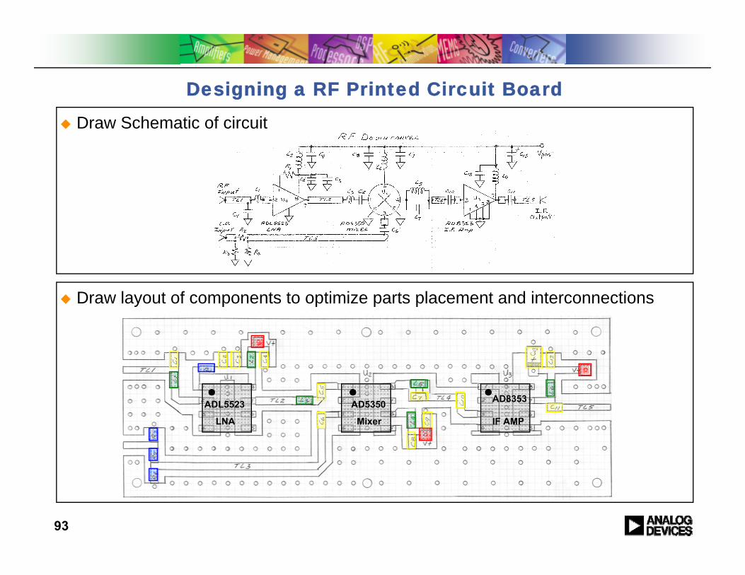
Designing a RF Printed Circuit Board
Draw Schematic of circuit
Draw layout of components to optimize parts placement and interconnections
AD8353ADL5523 AD5350 AD8353
LNA Mixer IF AMP
93

Designing a RF Printed Circuit Board
Matching components placed close to RF device
Place bias line bypassing components close to RF
device
Large number of vias under devices to provide good RF grounds and
thermal conductivity
Ground vias at end of RF and bypass
components
Ground plane Is not close totransmission line to reduce
RF Input
line to reducecoupling
ADL5523 AD5350 AD8353LNA Mixer IF AMP
RF Input
IF Output
LO Input
Inductors placed at right angles to reduce coupling
of their magnetic fields
RF devices placed in a straight line to aid in overall circuit
stability
Short interstage RF transmission lines
between stages
Very short ground leads from device to ground plane
RF attenuator placed close to
board connector
94

Shielding on RF Circuit BoardsgOn multilayer circuit boards, use Stripline transmission lines if possibleRoute DC bias and signal traces on inner layers between the ground planesIf required, place shielded enclosures around the RF stages on the boardequ ed, p ace s e ded e c osu es a ou d t e stages o t e boa dBe careful as to the physical size of the shielded enclosures, as it could become a resonate “cavity” at the higher frequenciesTraces going to or from shielded sections should be routed on inner layers if possibleif possible
Shield enclosure outlines DC bias line on inner layer
ADL5523 AD5350 AD8353
LNA Mixer IF AMP
D C BiasRF Input
IF Output
All board mounting holes should be On multilayer board use stripline
L O Input
95
All board mounting holes should be plated through to provide good RF
grounds to the external housing
On multilayer board use stripline transmission lines to provide
shielding

Th W ld L d i Hi h P f Si l P i S l tiThe World Leader in High Performance Signal Processing Solutions
Checking the Layout

Checking the Layoutg y
Design reviewgColleague review
97

Checking the Layoutg y
Design reviewgColleagueColored pencils
Old SchoolOld SchoolHelps trace signal path on schematic and PCB
98

Checking the Layoutg y
Design reviewgColleagueColored pencils
Old SchoolOld SchoolHelps trace signal path on schematic and PCB
Sit with the designer whenSit with the designer when board corrections are made
Trust no oneA change in one area of theA change in one area of the board could inadvertently change another part of the board
99

Next Stepsp
Order BoardsBuild and testEvaluate performanceIterate and try again if requiredIterate and try again if requiredSuccessful High Speed/RF PCB design is a combination of education and experience
100

Th W ld L d i Hi h P f Si l P i S l tiThe World Leader in High Performance Signal Processing Solutions
Summary

Summaryy
High speed PCB design requires deliberate thought and attention to detail!Load the schematic with as much information as possibleWhere you put individual components on the board is just as important as to where you put entire circuitsTake the lead when laying out your board, don’t leave anything to chanceUse multiple capacitors for power supply bypassingUse multiple capacitors for power supply bypassingParasitics must be considered and dealt withGround and Power planes play a key role in reducing noise and parasiticsNew packaging and pinout options allow for improved performance andNew packaging and pinout options allow for improved performance and more compact layoutsThere are many options for signal distribution, make sure you choose the right one for your applicationCh k th l t d h k it iCheck the layout and check it againSuccessful High Speed PCB design is a combination of education and experience and sometimes a little luck!
102

Summaryy
Work directly with PC board designer as they most likely will not understand proper RF layout techniquesP id d i ith d i f th l ti f th iti l hi hProvide designer with a drawing of the location of the critical high frequency components and transmission lines Instruct the board designer that transmission line widths and lengths are very critical and must be exactly as calculatedg y yPlace the components to minimize the length of RF interconnectionsGenerally try to place components in a “straight line” to avoid feedback loops and instabilitiesfeedback loops and instabilitiesPlace circuit blocks such as oscillators, mixers, amplifiers in separate sections on the board if possibleDo NOT mix digital, low level analog, or bias traces with RF g , g,interconnects to avoid unwanted couplingLocate the components operating at the highest frequencies close to board interconnectsWith the PC board designer check and recheck the layout before
103
With the PC board designer, check, and recheck the layout before sending out for fabrication

ReferencesArdizzoni, John “A Practical Guide to High-Speed Printed-Circuit-Board Layout ”Ardizzoni, John, “Keep High-Speed Circuit-Board Layout on Track,” Ardizzoni, John, Keep High Speed Circuit Board Layout on Track, EE Times, May 23, 2005.Brokaw, Paul, “An IC Amplifier User’s Guide to Decoupling, Grounding, and Making Things Go Right for a Change,” Analog Devices Application Note AN-202.Brokaw, Paul and Jeff Barrow, “Grounding for Low- and High-Frequency Circuits,” Analog Devices Application Note AN-345.Buxton, Joe, “Careful Design Tames High-Speed Op Amps,” Analog Devices Application Note AN-257.DiSanto, Greg, “Proper PC-Board Layout Improves Dynamic Range,” EDN, November 11, 2004.Grant, Doug and Scott Wurcer, “Avoiding Passive-Component Pitfalls,” Analog Devices Application Note AN-348Johnson, Howard W., and Martin Graham, High-Speed Digital Design, a Handbook of Black Magic, Prentice Hall, 1993.Jung, Walt, ed., Op Amp Applications Handbook, Elsevier-Newnes, 2005 available on Amazon.com
104
Kester, Walt, The Data Conversion Handbook, Elsevier-Newnes, 2005 available on Amazon.com

References
Hartley, Rick, “RF / Microwave PC Board Design and Layout”y g yReed, Dale, RF and Microwave Basics Impact PCB DesignMercer, Sean, “Minimizing RF PCB Electromagnetic Emissions,” RF Design, January 1999.Fabian Kung Wai Lee, “Open notes on High-Speed Printed CircuitBoard (PCB) Design (August 2008) “ Available at http://persona.mmu.edu.my/~wlkung/ADS/ads.htm”H H l “St i li Ci it D i ”Howe, Harlan, “Stripline Circuit Design”Rogers Corporation, “A Low cost Laminate for WirelessApplications,” Microwave Journal, Sept 1996Rogers Corporation “Microwave Impedance Calculator (MWIJ 1 0)”Rogers Corporation, “Microwave Impedance Calculator (MWIJ 1.0)”
105

Contact Information
John Ardizzoni Dennis FallsAnalog Devices, Inc.804 Woburn StreetWilmington MA 01887 1017
Avnet Electronics Marketing9200 Indian Creek ParkwaySuite 600Wilmington, MA 01887-1017
Email:
Suite 600Overland Park, Kansas 66210
[email protected] E-mail:[email protected]
106

Th W ld L d i Hi h P f Si l P i S l tiThe World Leader in High Performance Signal Processing Solutions
Thank You