printed circit board layot · printed circit board layot specializing in high-performance pcbs t...
TRANSCRIPT

PRINTED CIRCUIT BOARD LAYOUTSpecializing In High-Performance PCBs
Manufacturing That Eliminates Risk & Improves Reliability www.epectec.comToll Free: (888) 995-5171
Definition: Providing the physical printed circuit board layout of your completed schematic design.
Schematic Input Format/Supported Software• Eagle • DXF • PDF • Allegro• OrCAD • Design Spark • Gerber • Image File• ASCII • Cadence • PADS • Altium
Board Details Needed1. Board Outline Dimensions, 1:1 Drawing, or detailed info.2. Technology (SMD/Thru-Hole, Mixed, Double Sided Component Placement.3. Any test points or programming points needed?4. Key Component Locations and Locations of any artwork/logos.5. Netlist or Block Diagram if available.
Listing of Unusual Requirements:• Gold Fingers • Min Tolerances • High Currents/Voltages• Thickness Constraints • Keep Out Locations • Star Grounds• Controlled Impedance • Differential Pairs • Min/Max Spacing• High Frequency • Cutouts/Mounting Holes • Target Layer Count• IPC / Mil Spec / ITAR • Via Fill • RoHS
Bill Of Materials (BOM) Requirements• Complete component list with manufacturers part numbers.• Data sheets for custom/non standard components.
Special Customer Requirements• Will customer be seeking UL, CE, FCC or IEC certification or approval?• If processors are used, who will be providing the programming?• What is the desired timeline for completion of the project?
Epec DeliverablesDescription Format Description Format
Gerber Files • RS 274X Pick and Place • ExcelFabrication Drawing • RS274X, PDF Assembly Drawings • RS274X, PDFNative CAD database • Various Design Database Files • AllegroNetlist • IPC-D-356A ODB++ Files (If required) • ZIP / TARNC Drill File • Excellon 3D Models (If required) • STP Files
TimelinesQuotes: 2 - 5 Days From The Day The Quote Request Is Submitted.Usually includes a conference call to discuss requirements on complex designs.Standard Layout Delivery - 2-3 Weeks (1 week with a premium)Complexity (layer count, high speed, analog, number of nets) will determine actual lead time.Lead time will be outlined on the quote provided.
Manufacturing That Eliminates Risk & Improves Reliability www.epectec.comToll Free: (888) 995-5171
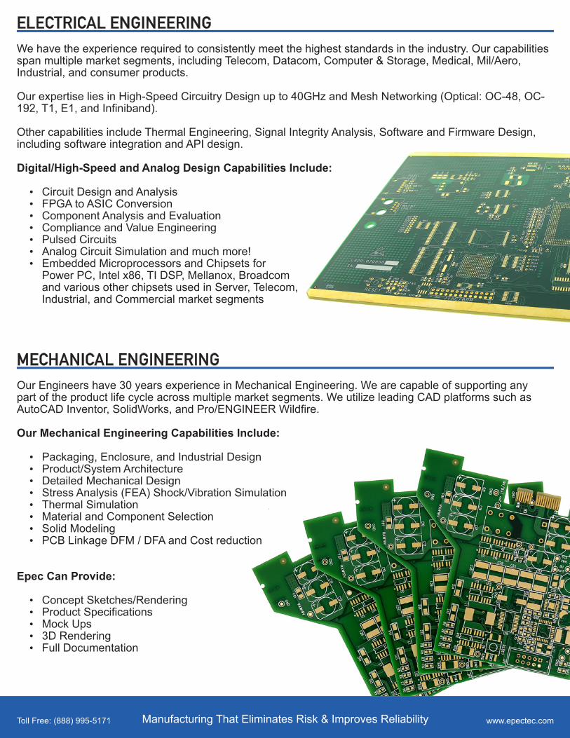
We have the experience required to consistently meet the highest standards in the industry. Our capabilities span multiple market segments, including Telecom, Datacom, Computer & Storage, Medical, Mil/Aero, Industrial, and consumer products.
Our expertise lies in High-Speed Circuitry Design up to 40GHz and Mesh Networking (Optical: OC-48, OC-192, T1, E1, and Infiniband).
Other capabilities include Thermal Engineering, Signal Integrity Analysis, Software and Firmware Design, including software integration and API design.
Digital/High-Speed and Analog Design Capabilities Include:
• Circuit Design and Analysis• FPGA to ASIC Conversion• Component Analysis and Evaluation• Compliance and Value Engineering• Pulsed Circuits• Analog Circuit Simulation and much more!• Embedded Microprocessors and Chipsets for
Power PC, Intel x86, TI DSP, Mellanox, Broadcom and various other chipsets used in Server, Telecom, Industrial, and Commercial market segments
Our Engineers have 30 years experience in Mechanical Engineering. We are capable of supporting any part of the product life cycle across multiple market segments. We utilize leading CAD platforms such as AutoCAD Inventor, SolidWorks, and Pro/ENGINEER Wildfire.
Our Mechanical Engineering Capabilities Include:
• Packaging, Enclosure, and Industrial Design• Product/System Architecture• Detailed Mechanical Design• Stress Analysis (FEA) Shock/Vibration Simulation• Thermal Simulation• Material and Component Selection• Solid Modeling• PCB Linkage DFM / DFA and Cost reduction
Epec Can Provide:
• Concept Sketches/Rendering• Product Specifications• Mock Ups• 3D Rendering• Full Documentation
MECHANICAL ENGINEERING
ELECTRICAL ENGINEERING