high speed on-chip measurement circuit - diva - simple search
TRANSCRIPT

HIGH SPEED ON-CHIPMEASUREMENT CIRCUIT
By
Arvid Stridfelt
Reg nr: LiTH-ISY-EX-3599-2005
Linköping 2005-01-05


HIGH SPEED ON-CHIPMEASUREMENT CIRCUIT
Master Thesis
Division of Electronic Devices
Department of Electrical Engineering
Linköping University
By
Arvid Stridfelt
Reg nr: LiTH-ISY-EX-3599-2005
Supervisor: Atila Alvandpour
Examiner: Atila Alvandpour
Linköping, February 17, 2005.


Avdelning, InstitutionDivision, Department
Institutionen för systemteknik581 83 LINKÖPING
DatumDate2005-02-17
SpråkLanguage
RapporttypReport category
ISBN
Svenska/SwedishX Engelska/English
LicentiatavhandlingX Examensarbete
ISRN LITH-ISY-EX-3599-2005
C-uppsatsD-uppsats
Serietitel och serienummerTitle of series, numbering
ISSN
Övrig rapport____
URL för elektronisk versionhttp://www.ep.liu.se/exjobb/isy/2005/3599/
TitelTitle
Inbyggd krets för höghastighetsmätning på chip
High Speed On-Chip Measurment Circuit
Författare Author
Arvid Stridfelt
SammanfattningAbstract
This master thesis describes a design exploration of a circuit capable of measuring high speed signalswithout adding significant capacitive load to the measuring node.
It is designed in a 0.13 CMOS process with a supply voltage of 1.2 Volt. The circuit is a master andslave, track-and-hold architecture incorporated with a capacitive voltage divider and a NMOS sourcefollower as input buffer to protect the measuring node and increase the input voltage range.
This thesis presents the implementation process and the theory needed to understand the designdecisions and consideration throughout the design.
The results are based on transistor level simulations performed in Cadence Spectre. The results showthat it is possible to observe the analog behaviour of a high speed signal by down converting it to alower frequency that can be brought off-chip. The trade off between capacitive load added to themeasuring node and input bandwidth of the measurment circuit is also presented.
NyckelordKeywordCMOS, 0.13, sampling, periodic sampling, digital oscilloscope, time equivalent sampling, track andhold, master and slave, sampling clock generator, voltage divider, source follower, sampling switch,transmission gate, RLC-line


i
ABSTRACT
This master thesis describes a design exploration of a circuit capable of measuring high speed signals without adding signifi-cant capacitive load to the measuring node.
It is designed in a 0.13 CMOS process with a supply voltage of 1.2 Volt.
The circuit is a master and slave, track-and-hold architecture incorporated with a capacitive voltage divider and a NMOS source follower as input buffer to protect the measuring node and increase the input voltage range.
This thesis presents the implementation process and the theory needed to understand the design decisions and consideration throughout the design.
The results are based on transistor level simulations performed in Cadence Spectre. The results show that it is possible to observe the analog behaviour of a high speed signal by down converting it to a lower frequency that can be brought off-chip. The trade off between capacitive load added to the measuring node and input bandwidth of the measurment circuit is also pre-sented.

ii

iii
ACKNOWLEDGEMENTS
I would like to thank some persons that has made the work on this master thesis possible one way or another.
• My supervisor and examiner Professor Atila Alvandpour for his advice, help, and support during this project.
• PhD students Behzad Mesgarzadeh, Kalle Folkesson, Martin Hansson and Peter Caputa. They have helped me by answering my many questions about everything.
• Professor Christer Svensson for giving me very valuable tips dur-ing the design. Professor Jerzy Dabrowski for helping me under-stand some frequency domain issues.
• My roommates at work, Rebecca Källsten and Christian Kullberg, for discussions about more or less electronic related topics.
• All my friends who has made the time spend on this master thesis and the last five years enjoyable.
• My girlfriend for having patience with my many late hours.
• The rest of the members of the Electronic Devices group for creat-ing an enjoyable working atmosphere.

iv

1
TABLE OF CONTENTS
Abstract i
Acknowledgements iii
1 Introduction 11.1 Purpose. . . . . . . . . . . . . . . . . . . . . . . . . . . . . . . . . . . . . . . . . . . . . 21.2 Reading guidelines. . . . . . . . . . . . . . . . . . . . . . . . . . . . . . . . . . . . 21.3 Abbreviations. . . . . . . . . . . . . . . . . . . . . . . . . . . . . . . . . . . . . . . . 3
2 Sampling Theory 52.1 Basics of sampling . . . . . . . . . . . . . . . . . . . . . . . . . . . . . . . . . . . . 5
2.1.1 Sampling theorem . . . . . . . . . . . . . . . . . . . . . . . . . . . . . . . . . 52.1.2 Bandpass sampling . . . . . . . . . . . . . . . . . . . . . . . . . . . . . . . . 72.1.3 Aliasing . . . . . . . . . . . . . . . . . . . . . . . . . . . . . . . . . . . . . . . . . 82.1.4 Periodic sampling . . . . . . . . . . . . . . . . . . . . . . . . . . . . . . . . . 9
2.2 Real time sampling . . . . . . . . . . . . . . . . . . . . . . . . . . . . . . . . . . 102.3 Time equivalent sampling . . . . . . . . . . . . . . . . . . . . . . . . . . . . . 102.4 Topologies of digital oscilloscopes off-chip . . . . . . . . . . . . . . . 11
2.4.1 DSO topology . . . . . . . . . . . . . . . . . . . . . . . . . . . . . . . . . . . 112.4.2 Sampling oscilloscope topology . . . . . . . . . . . . . . . . . . . . . 12
3 System Description 133.1 Alternative system architectures . . . . . . . . . . . . . . . . . . . . . . . . 13
3.1.1 System with on-chip Sampling Clock Generator . . . . . . . . 143.1.2 System with External Sample Clock Generation. . . . . . . . . 153.1.3 System selection and motivation . . . . . . . . . . . . . . . . . . . . . 16
3.2 Sampling frequency in periodic sampling . . . . . . . . . . . . . . . . . 163.2.1 Requirements on sampling frequency . . . . . . . . . . . . . . . . . 163.2.2 Requirements on practical sampling frequency. . . . . . . . . . 18
3.3 Simulation . . . . . . . . . . . . . . . . . . . . . . . . . . . . . . . . . . . . . . . . . 203.3.1 Simulation setup . . . . . . . . . . . . . . . . . . . . . . . . . . . . . . . . . 203.3.2 Simulation results . . . . . . . . . . . . . . . . . . . . . . . . . . . . . . . . 23
4 Architectures and building blocks 254.1 Track-and-hold circuits . . . . . . . . . . . . . . . . . . . . . . . . . . . . . . . 254.2 Master and Slave sampler . . . . . . . . . . . . . . . . . . . . . . . . . . . . . 264.3 Source follower . . . . . . . . . . . . . . . . . . . . . . . . . . . . . . . . . . . . . 27

2
4.4 Switch structures . . . . . . . . . . . . . . . . . . . . . . . . . . . . . . . . . . . . 304.4.1 NMOS switch . . . . . . . . . . . . . . . . . . . . . . . . . . . . . . . . . . . 314.4.2 PMOS switch . . . . . . . . . . . . . . . . . . . . . . . . . . . . . . . . . . . . 334.4.3 Clock feed through and channel charge injection . . . . . . . . 344.4.4 Transmission-gate switch . . . . . . . . . . . . . . . . . . . . . . . . . . 364.4.5 Dummy transistor . . . . . . . . . . . . . . . . . . . . . . . . . . . . . . . . 384.4.6 Linearized switch. . . . . . . . . . . . . . . . . . . . . . . . . . . . . . . . . 394.4.7 Bootstrap switch . . . . . . . . . . . . . . . . . . . . . . . . . . . . . . . . . 40
5 Design and implementation 435.1 Requirements . . . . . . . . . . . . . . . . . . . . . . . . . . . . . . . . . . . . . . . 435.2 The DSO and sampling oscilloscope on-chip . . . . . . . . . . . . . . 44
5.2.1 Architecture example - sampling oscilloscope on-chip. . . . 445.2.2 Architecture example - DSO on-chip . . . . . . . . . . . . . . . . . 465.2.3 Motivation of selected architecture . . . . . . . . . . . . . . . . . . . 46
5.3 Implementation plan . . . . . . . . . . . . . . . . . . . . . . . . . . . . . . . . . 475.3.1 Voltage range and input buffer . . . . . . . . . . . . . . . . . . . . . . 475.3.2 Master switch. . . . . . . . . . . . . . . . . . . . . . . . . . . . . . . . . . . . 515.3.3 Master buffer . . . . . . . . . . . . . . . . . . . . . . . . . . . . . . . . . . . . 535.3.4 Slave switch . . . . . . . . . . . . . . . . . . . . . . . . . . . . . . . . . . . . . 545.3.5 Slave buffer . . . . . . . . . . . . . . . . . . . . . . . . . . . . . . . . . . . . . 54
5.4 Implementation . . . . . . . . . . . . . . . . . . . . . . . . . . . . . . . . . . . . . 545.4.1 Slave buffer . . . . . . . . . . . . . . . . . . . . . . . . . . . . . . . . . . . . . 545.4.2 Integration slave switch - slave buffer. . . . . . . . . . . . . . . . . 565.4.3 Integration master buffer - slave switch - slave buffer . . . . 615.4.4 Integration master switch - master buffer - slave switch -
slave buffer . . . . . . . . . . . . . . . . . . . . . . . . . . . . . . . . . . . . . 625.4.5 Integration voltage divider - input buffer - master switch -
master buffer - slave switch - slave buffer. . . . . . . . . . . . . . 63
6 Results and discussion 696.1 Input capacitance vs. bandwidth . . . . . . . . . . . . . . . . . . . . . . . . 69
6.1.1 1:1 ratio . . . . . . . . . . . . . . . . . . . . . . . . . . . . . . . . . . . . . . . . 696.1.2 5:1 ratio . . . . . . . . . . . . . . . . . . . . . . . . . . . . . . . . . . . . . . . . 70
6.2 Sampling example . . . . . . . . . . . . . . . . . . . . . . . . . . . . . . . . . . . 716.3 Conclusions . . . . . . . . . . . . . . . . . . . . . . . . . . . . . . . . . . . . . . . . 756.4 Personal reflections . . . . . . . . . . . . . . . . . . . . . . . . . . . . . . . . . . 75
6.4.1 Future improvements . . . . . . . . . . . . . . . . . . . . . . . . . . . . . . 76
7 References 77Appendix A: Simulation Parameters 79

1
1INTRODUCTION
As the speed in digital design increases, the design will be more affected by analog issues i.e. inductive and capacitive crosstalk. Relative timing between signals also becomes more important as speed increases. System-on-Chip design is becoming more common, the need for testing analog blocks embedded in digital integrated circuits also increases.
There are few alternatives to monitor the analog behaviour of a digital signal, analog buffers can be used to bring a signal off-chip, but are limited to a few hundred MHz. Microprobing or E-beam probing is very expensive and require available top-level metal for probing.
There are oscilloscopes that actually can perform sampling of periodic signals of very high frequency. The problem is to bring this very high frequency signal of chip.
Traditional on-chip testing in digital design such as automatic test pattern generation (ATPG) and built-in self-test (BIST) are limited by the binary abstraction and are usually used in lower speeds. Their focus is on the functionality, and cannot adress the analog behaviour of a signal.

2
1.1 Purpose
The purpose of this project is to perform a design exploration for a high-speed on-chip measurement circuit, which adds as little capacitive load to the measuring node as possible. The measure-ment circuit uses the principle of periodic sampling, to down-convert periodic signals to lower frequency, which are possible to bring off-chip and measure with standard equipment.
The schematic design and simulation is to be performed in a 0.13 process with supply voltage of 1.2 V.
1.2 Reading guidelines
The reader should have a good understanding of standard CMOS digital design. Basic knowledge about the MOSFET tran-sistor is also required since this theory is not covered in this report.
Chapter 2 and 3 presents some background theory that is needed to understand the design discussions in the chapters that follows.
Chapter 2 - Theory
The basic theory regarding sampling is presented. Related infor-mation regarding off-chip oscilloscopes are also presented.
Chapter 3 - System description
The project is discussed at a system level, and from the future users point of view. Some additional theory needed to under-stand the system description is presented.
Chapter 4 - Presentation of different structures
A brief presentation of the main structures of track and hold cir-cuits are presented here. Different structures of the building
µm

3
blocks such as buffers and switches are also presented.
Chapter 5 - Design and implementation
The design methodology is described and the different struc-tures of each building block is compared, selected and moti-vated.
Chapter 6 - Results and conclusions
The simulation results of some different designs of the chosen topology is presented. Discussion and conclusions regarding the design are presented.
References
A list of all references in this report.
1.3 Abbreviations
ATPG - Automatic Test Pattern Generation
BIST - Built-In Self-Test
CMOS - Complementary Metal Oxide Semiconductor
IF - Intermediate Frequency
LPF - Low Pass Filter
MOSFET - Metal Oxide Semiconductor Field Effect Transistor
NMOS - Negative-channel Metal Oxide Semiconductor
PLL - Phase Locked Loop
PMOS - Positive-channel Metal Oxide Semiconductor
RF - Radio Frequency
SCG - Sampling Clock Generator
VTC - Voltage Transfer Characteristics

4

5
2SAMPLING THEORY
This chapter covers the basic theory regarding sampling and how it is used in real time sampling and time equivalent sam-pling performed by digital oscilloscopes [1]. Essential informa-tion about off-chip oscilloscopes are also presented.
2.1 Basics of sampling
Sampling is the operation of converting a time and amplitude continuos signal to a number of electrical values. These electrical values are discrete in time but continuos in amplitude, and each sampling point is ideally equal to the amplitude of the sampled signal at the time instant the sample was taken.
Usually some sort of A/D-convertion is performed on these val-ues to make them discrete in amplitude as well. The samples are converted to a binary representation, which opens possibilities of digital storing and processing.
If certain rules regarding the sampling process are fulfilled, the original signal can be reconstructed from the previous taken samples.
2.1.1 Sampling theorem
If a signal that is band limited in frequency is sampled it can,

6
theoretically, be fully restored if the sampling frequency is selected in a proper way. The sampling theorem states that a sig-nal can be fully restored if the sampling frequency is higher than twice the highest frequency component of the original signal. In the time domain this means that there will be at least two sam-ples whitin the period time of the highest frequency component. If this is fulfilled, enough information regarding the original sig-nal is in the samples to ensure a correct reconstruction. [2]
The sampling theorem can be expressed both in frequency- and time-domain:
(2.1)
(2.2)
Where is the sampling frequency, is the bandwidth of the
signal that is sampled, is the sampling period and is the
periodtime of the highest frequency component in the original signal. Observe that the original signal is assumed to contain fre-quency components from DC ( ) to . [2]
If these requirements are fulfilled the signal spectrum of the original signal and the sampled signal looks like figure 2.1.
f s 2 f 0>
T s12---T 0<
f s f 0
T s T 0
f 0= f f 0=

7
Figure 2.1 Signal sampled at . a) original spectrum, b) spectrum of the sampled signal.
The sampled signals spectrum will be repeated at a rate defined by the sampling frequency. The unwanted higher frequencies that is produces can easily be filtered out with a LPF (Low Pass
Filter) with a cutoff-frequency equal to . [2]
2.1.2 Bandpass sampling
For signals which do not extend to dc, the minimum required sampling rate is a function of the bandwidth of the signal as well as its position in the frequency spectrum.
If a signal is limited to a certain frequency-band, , it
is possible to reconstruct the original signal when it is sampled at [2]. This type of sampling is referred to by
many names such as Bandpass sampling [3], IF sampling, Harmonic sampling [4], Sub-Nyquist sampling and under sampling [5]. This type of sampling is common in applications like digital receiv-ers. This is however in the realm of RF and will not be utilized in
f0-f0
f0-f0 fsfs
fs/2-fs/2
a)
b)
f s 2 f 0>
f s
2-----
f 1 f 0 f 2< <
f s 2 f 2 f 1–( )>

8
this work.
2.1.3 Aliasing
If a signal that is limited in bandwidth is sampled with a fre-quency that does not fulfil the sampling theorem, it is not guar-anteed that the original signal can be reconstructed. In figure 2.2it is visible what could happen if a signal is sampled at a sam-pling frequency that violates the sampling theorem.
Figure 2.2 Signal sampled at , a) original spectrum b) aliased spectrum.
The different repetitions of signal spectrum of the discrete sig-nal, will overlap each other. High-frequency component are “folded down” to a lower frequency. If the sampled signal that is aliased would be filtered in a LPF with a cutoff-frequency
equal to , a distorted signal would be the result, since the sig-
nal spectrum is no longer identical to the spectrum of the origi-nal signal. [2]
f0-f0
f0-f0
fs
fs/2-fs/2
a)
b)
-fs
f s 2 f 0<
f s
2-----

9
2.1.4 Periodic sampling
If a signal is repetitive, it is possible to perform a sampling at a much lower frequency than in the case of real time sampling. Most signals are in fact periodic, or can at least be presented in a repetitive manner.
If a periodic signal has the period time and a sample is taken
at a certain time-point in the signal, the next sample can be taken later, where . New information of the signal is
thus gathered. This second sample can in fact be taken
later. Where is an integer and defines the number of periods later. The sampling period is thus related to the periodtime in the following way:
(2.3)
where is the sampling period, is period of the signal
and . In this way a very low can be used. The idea
can be visualised by figure 2.3. [8], [9], [10]
T d
T d ∆t+ ∆t T d«
nT d ∆t+
n
T s n, nT d ∆t n+ 1 2 3 …, , ,= =
T s n, T d
∆t T d n,« f s

10
Figure 2.3 Periodic sampling in the time domain.
The output frequency, or the beat frequency, , is the result of
the downconversion that occur when a multiple of the used sampling frequency is close to the data frequency. This can be expressed by
(2.4)
Where and . [14]
A derivation of the requirements of the sampling frequency is performed in section 3.2.1.
2.2 Real time sampling
In real time sampling the sampling frequency is chosen as high as possible. The goal is to collect as many samples as possible from a single sweep of a signal. The intention of real time sam-pling is to capture single shot signals, or transient signals.
To be able to sample a transient-event that has high frequency component it is necessary to have a high sampling rate. This is hard to implement and if is not high enough, aliasing will
occur.
In the realm of conventional digital oscilloscopes there is also a problem regarding the high speed memories that are needed to store the signal data acquired from a high-speed real time sam-pling after it has been digitalized. [1]
2.3 Time equivalent sampling
Digital oscilloscopes that performs time equivalent sampling utilizes periodic sampling. The use of time equivalent sampling opens possibilities for higher bandwidth of the oscilloscope since can be much lower than in the case of real time sam-
f b
f b f d n f s n,– n 1 2 3 …, , ,= =
n f s n,n
T s n,----------= f d
1T d------=
f s
f s

11
pling.
Depending on how the oscilloscope triggs the signal, two meth-ods are defined. The methods are random time equivalent sam-pling and sequential equivalent time sampling. [1]
In random equivalent time Sampling the samples are taken on a clock that runs asynchronously with respect to the input signal and the signal trigger. Samples are taken continuously, inde-pendent of the trigger position. The samples are sequential in time, but random with respect to the trigger. They are ordered from their relative position to the trigger. [1]
In sequential equivalent time Sampling one sample per trigger is taken. The trigger arrives at the same rate as the periods of data that is to be sampled. When a trigger is detected, a sample is taken in a short but well defined delay ( ). When the next trig-
ger is detected this delay is incremented ( ). [1]
2.4 Topologies of digital oscilloscopes off-chip
There are two main architectures of digital oscilloscopes. Both sample the signal in some way, yet one architecture is known as “sampling oscilloscope” and the other as “DSO” (digital storage oscilloscope).
The difference between the architectures lies in how the incom-ing signal is received. This difference leads to different attributes of the oscilloscopes.
2.4.1 DSO topology
This is the conventional type of oscilloscope. The input signal is attenuated and then amplified to have a voltage range and dc-level that suits the actual sampler. The architecture can be seen in figure 2.4
∆t
2∆t

12
Figure 2.4 DSO topology.
Since the sampler is protected by the attenuator/amplifier, the input voltage range can be about 50 to 100 volts [1]. The draw-back is that the input bandwidth is at the same time restricted to the bandwidth of the attenuator/amplifier.
Time equivalent sampling can be performed but since the band-width is limited it can not be exploited at its full extent. [1]
2.4.2 Sampling oscilloscope topology
This architecture can exploit more of the potential of time-equiv-alent sampling. The signal is sampled without any attenuation/amplification-unit at the input. When the signal has been down-converted to a lower frequency it is amplified by an amplifier with low input bandwidth. The architecture can be seen in fig-ure 2.5
Figure 2.5 Sampling oscilloscope.
This leads to a very high input bandwidth of the oscilloscope, but on the other hand hard restrictions of the input signals volt-age range. Most sampling oscilloscopes has a 1V peak to peak dynamic range. [1]
Attenuator Amplifier SamplingUnit
OscilloscopeInput
SamplingUnit
OscilloscopeInput Amplifier

13
3SYSTEM DESCRIPTION
This chapter describes the on-chip sampling oscilloscope in its context from a high level. No details about design of the differ-ent blocks are given. Design decisions on a system level are taken and motivated.
It is also covered how a possible user might use the oscilloscope. Theory about how to choose a proper sampling frequency is derived. This theory is also tested on a measuring circuit built with ideal components.
3.1 Alternative system architectures
The ideal on-chip sampling oscilloscope is supposed to measure the analog behaviour of very high speed periodic signals with-out adding significant load to the signal source. The signal source could be any kind of wire that carries a signal.
The signal that is brought off chip via an ordinary analog pad is monitored through an ordinary oscilloscope that is standard equipment in most laboratories.
There are two main architectures.
1) The sampling clock is generated by an external clock generator
2) The sampling clock is generated on-chip by a Sampling Clock Genera-

14
tor (SCG).
3.1.1 System with on-chip Sampling Clock Generator
This system can be understood from figure 3.1.
Figure 3.1 System with on-chip Sampling Clock Generator.
In this system the user does not need to take the sampling fre-quency into consideration. This signal is generated on-chip by a Sampling Clock Generator (SCG). This type of system can be found in [7], [8] and [9].
The benefits of this system is that the user does not need to be concerned by choosing a correct sampling frequency, all this is taken care of by the SCG. The requirements on the test environ-ment is relaxed since a well defined signal generator is not needed for sampling clock generation.
The typical way to implement the SCG is to use a Voltage Con-trol Delay Line based approach. In this way is controlled
Circuitry
clk
ON-CHIP OFF-CHIP
Oscilloscope
On-chipMeasurment
Circuit
Low FrequencyFrequency
High
Sampling Clock Generator
Sampling clk
clk
ON-CHIP OFF-CHIP
Oscilloscope
On-chipMeasurment
Circuit
Low FrequencyFrequency
High
∆t

15
rather than . A PLL (Phase Locked Loop) approach is not
suitable since the generation of would be dependent on the clock frequency, which is not wanted. The PLL approach also consumes more area and offers less portability [7].
3.1.2 System with External Sample Clock Generation
This system can be understood from figure 3.2
Figure 3.2 System with External Sampling Clock Generator.
In this system the sampling clock is generated off-chip in an external signal generator. This type of system can be found in [10].
The benefits of this system is that the measuring tool consumes a smaller area and the complexity of the chip is reduced compared to the system with SCG.
The drawbacks is that the measuring tool consumes one extra input to the chip and a good signal generator is required. Thus a more complex laboratory environment is required.
T ∆t+
∆t
Circuitry
Sampling clk
clk
ON-CHIP OFF-CHIP
Oscilloscope
On-chipMeasurment
Circuit
Low FrequencyFrequency
High

16
The user need to have good knowledge about the signal that is supposed to be measured. It is also required that the user from this knowledge can derive a suitable sampling frequency.
3.1.3 System selection and motivation
A system with an on-chip SCG could be better in a certain case of signal to measure. If the signal to be measured always has the same period and the on-chip SCG is implemented with respect to this. In this case it does not allow signals with different period time. The complexity of an on-chip SCG increases if signals with different period times is to be measured. The cost, limited design time and complexity of this system puts it beyond the scope of this master thesis. The system with off-chip sample clock generation is chosen so that more time can be allocated on implementing a sampling unit. An off-chip SCG is also better since it does not limit the usability in any sence. If a signal has a different period time, the sampling frequency can be adjusted manually without any extra hardware on-chip.
3.2 Sampling frequency in periodic sampling
Since the system with external sample clock generation is cho-sen it is required that the user manually adjusts the sampling frequency.
It is neccesary to have a good understanding of how the sam-pling frequency relates to the data that is to be sampled. It is also important to understand which requirements on the sampling frequency that has to be fulfilled in order to achieve a correct periodic sampling.
3.2.1 Requirements on sampling frequency
To achieve a correct output signal when performing periodic sampling I have derived requirements that have to be fulfilled regarding the sampling frequency. A correct output signal is defined as a signal that is not mirrored or aliased.

17
Parts of this discussion and derivation is based on the theory presented in section 2.1.
The constraints on the sampling frequency, is best under-
stood if they are derived from the constraints on . If the data will be sampled backwards, this leads to an output sig-nal that either is a mirrored image or an aliased mirrored image.
If the same point will be sampled each period, this leads to an output signal with a constant voltage value and
. Hence is the first constraint on that .
The upper boundary of is defined from the highest frequency
component of the data, .
In ordinary sampling two samples within the period time of the highest frequency component is at least needed. Since the peri-ods in a periodic signal are identical, the samples can be taken at two different periods. To make sure that we still get two samples within the period time of the highest frequency component has to be smaller than half the periodtime of the highest fre-quency component. This sets the second constraint on as
. Notice the similarity to the sampling theorem. Con-
sequently the requirement on is formulated as
(3.1)
Combining (2.3) and (3.1) we get
This can be rewritten as
f s n,
∆t ∆t 0<
∆t 0=
f b 0= ∆t 0 ∆t<
∆t
f hfc
∆t
∆t
∆t12---T hfc<
∆t
0 ∆t 0.5T hfc< <
0 T s n, nT d–12---T hfc< < nT d T s n,
12---T hfc nT d+< <⇔ ⇔
nf d------ 1
f s n,---------- 1
2 f hfc------------- n
f d------+< < 1
12 f hfc------------- n
f d------+
-------------------------- f s n,f d
n------< <⇔

18
(3.2)
If (3.2) is fulfilled the periodic sampling will be correctly per-formed without aliasing.
In ordinary sampling that fulfils (2.2), all information about the original signal is in the samples. In periodic sampling the infor-mation of the original signals frequency is not in the samples. So the trade-off is that the user has to gain knowledge regarding the original signal in some other way, but instead much faster signals can be sampled since the sampling rate can be low.
3.2.2 Requirements on practical sampling frequency
As can be seen in section 2.1.4 the sampling period relates to the period of data. An expression (3.2) for the constraints on the sampling frequency when a periodic sampling is performed was derived in 3.2.1.
The on-chip oscilloscope is assumed to measure periodic bit-streams. A square-wave consists of very high frequency compo-nents, but in the following discussion these high frequencies are not considered.
In a periodic bitstream it is assumed that at some point in the
bits are toggled at the fastest rate (usually ) i.e. the
duration of one bit equals . Thus:
To be sure to have a correct sampling, it is common [11] that the second constraint on is written
(3.3)
This means that we need at least five samples within the period-
2 f hfc f d
f d 2nf hfc+---------------------------- f s n,
f d
n------ n< < 1 2 3 …, , ,=
12--- f sysclk
0.5T hfc
T hfc
T duration of one bit
2------------------------------------ =2T sysclk( )=
∆t
∆t15---T hfc≤

19
time of the highest frequency component. This will also be more suitable regarding the high frequency component in square-waves.
Following the previous derivation in section 2.1.4 we get
(3.4)
Equation (3.4) is theoretically valid, but for very high frequen-cies of data a problem occurs. If a sampling frequency that fulfils
the lower constraint of theoretically allowed is used, the
beat frequency, , will be relatively high. Notice that the basic
idea of an on-chip sampling unit is to produce a signal of low frequency that can be brought off chip without attenuation.
Example 3.1 explains the problem.
Example 3.1
We have a sinusiodal signal that has the frequency of 6
GHz. is chosen since a very good clock generator is available. It is also assumed that the high sampling sig-nal could be brought on-chip. Equation (3.4) gives that
If is chosen as low as possible, in this case 5 GHz,
according to (3.4).
If is instead chosen closer to the upper constraint, in
this case 5.98 GHz according to (3.4).
The in Example 3.1 is theoretically valid but does not fulfil
5 f hfc f d
f d 5nf hfc+---------------------------- f s n,≤
f d
n------ n< 1 2 3 …, , ,=
f s n,
f b
n 1=
5 6 9×10 6 9×10⋅ ⋅6 9×10 5 1 6 9×10⋅ ⋅+--------------------------------------------------- f s 1,≤ 6 9×10
1-------------- ⇔<
5 9×10 f s 1, 6 9×10<≤
f s 1,
f b1 f d 1 f s 1,⋅– 6 9×10 5 9×10– 1GHz= = =
f s 1,
f b2 f d 1 f s 1,⋅– 6 9×10 5.98 9×10– 20MHz= = =
f b1

20
the basic concept, it is not a signal that can be said to have low frequency. has a frequency that is more in line with the basic
concept.
The last buffer stage of the design will have a relatively low bandwidth to filter out noise from the sampled signal. The bandwidth of this stage will set a new requirement on the choice of sampling frequency. This requirement is added when this component has been implemented.
3.3 Simulation
A sampling unit has been constructed with ideal components in verilogA. At this stage it is not important which topology the sampling unit has, the theory regarding choosing a suitable sampling frequency should fit for all topologies that intends to perform periodic sampling. The last requirement on the sam-pling frequency relates to the attenuation of the last buffer stage in the sampling unit I intend to implement, and is not of interest at a system level. This requirement is therefor not tested at this stage.
3.3.1 Simulation setup
The sampler topology used in [12] was used as a model when creating ideal components.
The simple bit-stream in figure 3.3 was generated and sampled at different frequencies.
f b2

21
Figure 3.3 Simple bitstream.
The first test simulates when is set to be equal to 502MHz and
then swept down to 442MHz. According to 3.4 the range of suit-able sampling frequencies when sampling each period (n=1) is
..
Interval [us] Ts [ps] fs [MHz] fb [MHz] Result
0-0.8 1990 502.5 - mirrored
0.8-1.6 1995 501.2 - mirrored
1.6-2.4 2000 500 0 constant level
2.4-3.2 2005 498.7 1.25 correct
3.2-4.0 2010 497.5 2.49 correct
4.0-4.8 2015 496.3 3.72 correct
4.8-5.6 2020 495.0 4.95 correct
5.6-6.4 2025 493.8 6.17 correct
6.4-7.2 2030 492.6 7.39 correct
7.2-8.0 2050 487.8 12.2 correct
Table 3.1 n=1, one sample each period.
f s
476 f s 500< <

22
The simulation can be interpreted as if a user “turns the knob” on the signal generator that supplies the sampling frequency to the chip. Initially the user will se a mirrored waveform
, at a certain frequency a constant voltage will appear
, then a correct output signal will be achieved when
the correct region of is entered. As is further decreased
increases, and when the correct region of is passed, the
output signal becomes more and more aliased.
The second test simulates when is set to be equal to 501MHz
and then swept down to 166MHz. In this simulation it is verified that the output is correct in the intervals of that corresponds
to n = 2 and n = 3 as well.
8.0-8.8 2100 476.2 23.8 correct
8.8-9.6 2200 454.5 45.5 corrupted
9.6-10.4 2230 448.4 51.6 corrupted
10.4-11.2 2240 446.4 53.6 corrupted
11.2-12 2250 444.4 - corrupted
12-12.8 2260 442.5 - corrupted
n Interval [MHz]
1
2
3
Table 3.2 Intervals of for different values of n.
Interval [us] Ts [ps] fs [MHz] fb [MHz] Result
Table 3.1 n=1, one sample each period.
f s f d>( )
f s f d=( )
f s f s
f b f s
f s
f s
476.2 f s 1, 500< <
243.9 f s 2, 250< <
163.9 f s 3, 166.7< <
f s n,

23
The simulation can be interpreted as if a user “turns the knob” on the signal generator that supplies the sampling frequency to the chip. Three different correct regions of are passed.
3.3.2 Simulation results
The result shows that the derived requirements of is correct.
A future user might start at the known and gradually
decrease to find the first correct region. Or the user can use the
Interval [us] Ts [ps] fs
[MHz]fb
[MHz] Result n
0-0.8 1995 501.2 - mirrored -
0.8-1.6 2000 500 0 constant level
-
1.6-2.4 2010 497.5 2.49 correct 1
2.4-3.2 2030 492.6 7.39 correct 1
3.2-4.0 2100 476.2 23.8 correct 1
4.0-4.8 2260 442.5 - corrupted -
4.8-5.6 2800 357.1 - corrupted -
5.6-6.4 3000 333.3 - corrupted -
6.4-7.2 3500 258.7 - corrupted -
7.2-8.0 4000 250 0 constant level
-
8.0-8.8 4010 249.3 1.24 correct 2
8.8-9.6 4050 246.9 6.17 correct 2
9.6-10.4 4100 243.9 12.2 correct 2
10.4-11.2 4500 222.2 - corrupted -
11.2-12 6000 166.9 0 constant level
-
12-12.8 6020 166.1 1.66 correct 3
Table 3.3 n=1, n = 2, n = 3.
f s
f s
f s f d=

24
derived equations to find as many correct regions of as
wanted, and then choose a that is suitable.
f s
f s
25
4ARCHITECTURES AND BUILDING
BLOCKS
This chapter covers different track and hold circuits as well as different structures of building blocks such as buffers and switches.
When a complex analog design is implemented a division into smaller blocks is a good strategy to ensure an efficient imple-mentation process. Before any division and structured presenta-tion of possible blocks can be done, the general structure of the track and hold circuit has to be chosen.
4.1 Track-and-hold circuits
Track and hold circuits can be classified into two main classes: open-loop architectures and closed-loop architectures. These two classes are suitable for different areas. The open-loop archi-tectures is suitable for high speed but not high precision. The idea of this general structure can be seen in figure 4.1.

26
Figure 4.1 Open-loop track-and-hold circuit architecture.
The closed-loop architecture is a more complex structure and is suitable for high precision applications, but it lacks in speed. This type of general structure can be seen in figure 4.2
Figure 4.2 Closed-loop track-and-hold circuit architecture.
Since the goal is to sample as fast signals as possible, speed is a more attractive attribute than precision and linearity. Thus an open-loop track and hold circuit structure is chosen. [12], [18]
4.2 Master and Slave sampler
The regular sampler setup that is used in this type of applica-tions is a master-slave type track-and-hold sampler. This circuit is described in figure 4.3.
Vin Vout
Switch
Ch
B1 B2
Vin Vout
Switch
Ch
B1B2

27
Figure 4.3 Master and slave setup and basic idea.
The signal is sampled by the master switch on the sampling
clock. The value held on is resampled on a complementary
clock signal by the slave switch. High frequency components that are produced from the clock are filtered out by the last slave buffer, which usually has a low bandwidth to fulfil this task. The signal has been donwconverted to a lower frequency that can be brought off chip. [14]
4.3 Source follower
The source follower, also known as the common-drain stage, is often used as a voltage level shifter or as a buffer for a small swing signal driving a large capacitive load. A NMOS source follower is usually implemented as in figure 4.4
V in
mCh

28
Figure 4.4 Source follower with a NMOS transistor as cur-rent source.
The current source is implemented as a NMOS transistor biased into the saturation region via the current-mirror.
It can be replaced by a resistor but then the linearity of the input-output characteristics will be heavily dependent of the input dc-level.
The source follower senses the signal at the gate of and then drives the load at the source. The output follows the input with a voltage shift of . The VTC (Voltage Transfer Characteris-
tics) for a NMOS source follower can be studied in figure 4.5. [13]
Vdd
M1Vin
Vout
M2M3
Ibias
M 1
V GS

29
Figure 4.5 VTC of NMOS source follower.
To find an expression of the gain we need to study the small-sig-nal schematic of the source follower, figure 4.6
Figure 4.6 Small-signal schematic of NMOS source follower.
From figure 4.6 a node analysis can be performed:
(4.1)
From this the small-signal gain can be expressed as:
(4.2)
Vgs=Vin-Vout
+
-gm1(Vin-Vout)
1/gds1 1/gds2
gm1 V in V out–( )– V out gds1 gds2+( )+ 0=
AV out
V in----------
gm1
gm1 gds1 gds2+ +------------------------------------------ gm gds»{ } 1≈ ≈= =

30
Source followers has a high input impedance and a moderate output impedance which makes them good as buffers. They are not very linear and has voltage headroom limitation. The non-linearity that comes from the body-effect can be reduced by con-necting the bulk-terminal of transistor to its source-termi-
nal. Thus setting . [13]
The voltage headroom limitation is caused by the fact that the DC-level of the output signal is shifted by . For a NMOS-
source follower the signal is shifted down, and for a PMOS-source follower the signal is shifted up. [13]
As can be seen in figure 4.5 the VTC of the NMOS source fol-lower has most linear behaviour in the interval ~ V. This
is because transistor is in its strongest saturation region at
this input voltage levels. This means that a NMOS source fol-lower is preferred if the input voltage range is within this region. For a PMOS source follower it is the lower part of the voltage span that is suitable as input-range. [13]
4.4 Switch structures
The switch is an important part of a sampling unit. It is the switch that is supposed to sample a value at a capacitance, see figure 4.7.
M 1
V BS 0=
V GS
0.7 1.2–
M 1

31
Figure 4.7 Track and hold switch.
When the switch is closed, the output tracks the input. The out-put level is stored at the capacitance at the instant when the switch is opened, or turned off. The ideal switch has no resist-ance in closed mode and infinite resistance in open mode.
How fast and precise the switch can sample is determined by which type of switch that is used.
In CMOS-design there are three main types of switches. NMOS-, PMOS- and the transmission gate-switch. There are also differ-ent structures around these switches to improve linearity or pre-cision. The MOS-devices works well as switches, but they suffer from non-idealities which will be discussed in the following sec-tions. [13]
4.4.1 NMOS switch
The NMOS acting as a switch is the fastest and most simple switch in CMOS-design. As a sampling switch it is implemented as in figure 4.8
CLK
Vin Vout
Ch

32
Figure 4.8 NMOS transistor acting as a switch.
When is high, the NMOS transistor is on, and the switch is closed. The NMOS transistor is acting in the linear (triode) region and if it is assumed that the on-resist-
ance equal to [13]:
(4.3)
As can be understood by (4.3) and figure 4.9 the on-resistance is non-linear and dependent on the input voltage. If
then , and equivalently, the maxi-
mum output voltage that a NMOS transistor can deliver is equal to .
CLK
Vin Vout
Ch
CLK
CLKmax Vdd=
RON N,1
µnCoxWL----- V dd V in– V tn–( )
----------------------------------------------------------------=
V in V dd V T–→ RON N, ∞→
Vdd Vt–

33
Figure 4.9 Resistance of NMOS-transistor as function of input voltage.
The NMOS-transistor as a switch is thus most suitable for volt-age levels in the lower region of the voltage span. [13]
4.4.2 PMOS switch
The PMOS transistor acting as a switch is implemented like the NMOS it is implemented as in figure 4.8
The on-resistance of the PMOS transistor equals to:
(4.4)
As can be understood from (4.4) and figure 4.10 increases
towards infinity when approaches .
RON P,1
µ pCoxWL----- V in V tp–( )
----------------------------------------------------=
RON P,
V in V tp

34
Figure 4.10 Resistance of PMOS-transistor as function of input voltage.
The PMOS-transistor as a switch is most suitable for voltage lev-els in the upper region of the voltage span. [13]
4.4.3 Clock feed through and channel charge injection
There are two effects related to a MOS transistor acting as a switch in a track and hold setup that will produce a voltage off-set in the sampled voltage. These effects are clock feed through and channel charge injection. Figure 4.11 shows how these are related to the transistor.

35
Figure 4.11 Channel charge injection and clock feed through.
The charges that forms the channel when the transistor is on is injected to the drain and source terminals when the transistor is turned off. The charges that are injected to the terminal where the hold capacitance is connected will result in a offset voltage in the sampled voltage. If it is assumed that half of the charges are injected to either terminal this voltage is described by:
(4.5)
Where the denominator is the amount of charges that forms the channel. is the channel width, is the channel length, is
the gate oxide capacitance and is the hold capacitance. From
(4.5) it can be understood that the offset voltage depends on the input voltage level the relative sizing of the transistor and the hold capacitance.
Clock feed through is when a switch couples a clock transition through the gate-source of gate-drain overlap capacitance. This will add a constant offset voltage that is independent of the input voltage level and only dependent of the relative sizing of the transistor and the hold capacitance. The magnitude of the
...
...
V offset1
WLCox V dd V in– V th–( )2CH
-------------------------------------------------------------=
W L Cox
CH

36
offset voltage is described by:
(4.6)
Where is the overlap capacitance per unit width.
The total offset voltage that is added to the sampled voltage is the sum of the offset voltages related to channel charge injection and clock feed through.
(4.7)
[13].
4.4.4 Transmission-gate switch
The transmission gate as a sampling switch is implemented as in figure 4.12
Figure 4.12 Transmission-gate acting as a switch.
The on-resistance is more linear than a single MOS-transistor acting as a switch, since it consists of a NMOS- and a PMOS-transistor in parallel. [13]
If then can be written as
V offset2 V clk
W Cov
W Cov CH+-----------------------------=
Cov
V offset V offset1 V offset2+=
CLK
Vin Vout
Ch
CLK
µ pCoxWL-----⎝ ⎠
⎛ ⎞p
µnCoxWL-----⎝ ⎠
⎛ ⎞n
= RON TG,

37
(4.8). is then independent of the input voltage.
(4.8)
In figure 4.13, is compared to and . [13]
Figure 4.13 Resistance of transmission gate as a function of input voltage.
The transmission gate has the benefit that it can pass rail-to-rail signals, and as mentioned earlier, the on-resistance is more lin-ear than for a single MOS-device. If the transmission gate is properly sized can the errors caused by channel charge injection and clock feed through that was described in section 4.4.3 be reduced. The positive channel charge that is injected from the PMOS-transistor is cancelled by the negative channel charge injected from the NMOS-transistor. This is hard to accomplish since the channel charge is dependent on the input voltage level [13]. For a certain sizing the cancellation is only total for a cer-
RON TG,
RON TG, RON N, RON P,||
1
µnCoxWL-----⎝ ⎠
⎛ ⎞n
V dd V– tn V tp–( )---------------------------------------------------------------------------
=
=
RON TG, RON N, RON P,

38
tain voltage level. The clock feed through is suppressed since the transmission gate is driven by complementary clocks, but it is not complete because the gate-drain overlap capacitance is not equal for the NMOS and PMOS transistor.
The drawback is that it requires complementary clocks. If a cir-cuit consists of a large number of switches units, this will be a problem. The faster signal the transmission-gate is supposed to sample the more important will it be to have a very good com-plementary clock. If, for example, the PMOS transistor turns off
seconds after the NMOS device, the output will track the input during this time. The significant non linearity due to input dependency of the PMOS will add distortion to the output.
4.4.5 Dummy transistor
The purpose of the dummy transistor is to reduce the error caused by channel charge injection and clock feed through that was described in section 4.4.3. The dummy transistor is a single MOS transistor of the same type as the switch, and its source and drain terminals are shorted and connected to the switch output as can be seen in figure 4.14 It should be driven by the complement of the signal that drives the main switch.
The dummy transistor should be half the size of the sampling transistor. If it is assumed that 50% of the channel charge is injected towards the hold capacitance when the sampling tran-sistor turns off this charge will be absorbed by the dummy-tran-sistor when it turns on.
The positive feed through from the sampling switch is also can-celled by the negative feed through from the dummy-switch.
∆t

39
Figure 4.14 NMOS-switch and NMOS-dummy-transistor.
4.4.6 Linearized switch
In [14] a linearized switch is proposed. The idea is to keep
of the sampling switch constant. This will minimize the sam-pling errors due to variable on-resistance of the switch, input-dependent channel charge injection and the input dependent sampling instant variation. This switch is implemented as in fig-ure 4.15. The two buffers are source followers of PMOS type.
V gs

40
Figure 4.15 Linearized T/H circuit presented in [14].
4.4.7 Bootstrap switch
The idea of the bootstrapped switch [15] is similar to the linear-ized switch presented in section 4.4.6, to achieve a constant
for the sampling transistor. The idea is realized by connecting a voltage source between the input and the gate of the sampling transistor as can be seen in figure 4.16. The voltage source can be implemented as a capacitor that is disconnected and charged to
during hold mode. In track-mode it is connected between
input and gate and gives:
(4.9)
All problems related to dependency of are solved this way.
The drawbacks are that a gate voltage of the sampling transistor that exceeds can reduce the lifetime of the device [6]. Since
a continuous charging and discharging of a capacitor has to be performed the operation of the bootstrapped switch is limited for higher sampling frequencies.
SF
SF
Ch
VoutVin
CLK
V gs
V dd
V gs V dd V in V in–+ V dd= =
V gs
V dd

41
Figure 4.16 Bootstrapped NMOS-switch in track-mode.
SF
Ch
VoutVin
Vgs=Vdd+Vin-VinVdd

42

43
5DESIGN AND IMPLEMENTATION
This chapter describes the different levels of the design process. Different topologies are discussed from a higher abstraction level. When a topology is chosen the arrangement of each build-ing block is discussed from the “front-to-back” with respect to the chosen voltage range. The implementation is finally per-formed “back-to-front”, starting with the assumed 2.45pF capac-itance as load, see below for motivation.
All simulations are performed in Cadence spectre simulator.
5.1 Requirements
Since this is a design exploration, no specific requirements regarding input-bandwidth, capacitive load on the measure-ment node, power dissipation or other characteristics are set as specific requirements. The focus is to get as high bandwidth as possible, and at the same time add as little capacitive load as possible to the measurement node.
The linearity of the circuit is of some importance, but will not be given any heavy priority. In a design situation where linearity is the trade-off for high bandwidth or low capacitive load, the later properties will be favoured. The most important is that the input-output voltage transfer function never is “flat” for the designed input-voltage range. A flat voltage transfer function

44
means that several input-voltage levels generates the same out-put voltage.
The circuit should also be able to bring the resulting signal off-chip. The pad and the laboratory oscilloscope probe is assumed to have a capacitive load of 2.45pF. This figure was estimated from information regarding the top-metal and a 1.5pF labora-tory probe.
The circuit should be able to handle input rail-to-rail signals with 20% over- and under-shoot. The input voltage range is thus
for .
5.2 The DSO and sampling oscilloscope on-chip
The topology of the conventional DSO and sampling oscillo-scope that was presented in sections 2.4.1 and 2.4.2 can be implemented directly on-chip. The major properties of the two topologies will be similar on-chip, but will have different impact.
5.2.1 Architecture example - sampling oscilloscope on-chip
When a sampling oscilloscope is implemented on chip, there is no significant need for handling voltage swings that are much larger than rail-to-rail. Most signals are limited to the
range. A sampling oscilloscope architecture appears to be a good choice regarding this.
In a master and slave track-and-hold setup usually a buffer is inserted between the two switches. This buffer is often a source follower with the drawback of limited input voltage range. This source follower will be the component that limits the input volt-age range.
In [8] the problem of rail-to-rail input swing is solved by remov-ing the buffer between master and slave stage, see figure 5.1 to understand this setup.
0.24V V in 1.44V< <– V dd 1.2=
0 V dd–

45
Figure 5.1 Master and slave setup that performs charge shar-ing.
In this case a charge-sharing will occur between and ,
that divides the signal down to below . The idea is to
get the voltage range within the acceptable input range for the source follower of Ptype that follows the samplers. It is claimed that the input voltage range of the switches are -300mV to
. The supply voltage in this case is 2.5V which
means an input voltage range of . This means
that this architecture can detect voltage over- and under-shoots of ~12%. This is in fact limited by the treshold voltage of the transistors acting as master switch.
In the 0.13 process that is used in this project, the treshold voltage for the transistor is ~0.24V, which happen to be 20% of
.
This way of arranging the switches could give an acceptable input voltage range, the problem that can’t be overlooked is that
loads the measuring node when the master switch is
closed. It is also required that the master switch is implemented as a transmission-gate, which requires a very well defined com-plementary clock signal.
Vin Vout
clk
mCh sCh
master switch slave switchclk_bar
mCh sCh
V dd V tp–
V dd 300mV+
0.3V V in 2.8V< <–
µm
V dd
mCh

46
5.2.2 Architecture example - DSO on-chip
Since the requirement on the input signal is a voltage range of . The signal needs to be attenuated to a
more suitable range regarding the sampling switch, otherwise information of the signal will be lost. Compared to the conven-tional DSO:s, the input voltage range is relatively low, thus the bandwidth can be increased.
If a buffer in between the measuring node and the track-and-hold is used, the hold capacitance will not load the measuring node. As described in section 4.3 the usual source follower has a very high input impedance. This suits the requirements on the input buffer. The input impedance is expected to be much lower than the capacitive load would inflict.
In [12] a on-chip measurement circuit of this architecture is implemented. This circuit is designed with respect to rail-to-rail signal, it does not consider over- and under swings. It does not either investigate the trade-off between capacitive load and bandwidth. It is built from a certain requirement on bandwidth only. An common source stage is used as an input buffer, which has a higher capacitive input load than the source follower
5.2.3 Motivation of selected architecture
Since the capacitive load the circuit adds to the measuring node is of high priority, a conventional DSO architecture will be implemented. This leads to an architecture as in figure 5.2
0.24V V in 1.44V< <–
mCh

47
Figure 5.2 DSO-topology, mB/sB means master/slave-buffer.
The attenuator and buffer will be the critical point in the trade-off between input capacitive load and bandwidth.
5.3 Implementation plan
Since this 0.13 process has a of 1.2V, the implementation
process begins with an estimation of how this headroom will be used to its full extent.
The topology that will be implemented is discussed from front-to-back. Most considerations and some tests will be performed on the critical point; the attenuator and the input buffer. The dif-ferent building blocks are found in figure 5.3.
Figure 5.3 Building blocks and their order in the design.
5.3.1 Voltage range and input buffer
As stated in 4.3, the source followers that is used as buffers works best if the input voltage range is in the upper/lower 30% of the voltage range, depending if it is of N/Ptype. Following
Vout
clk
master switch slave switchclk_bar
Vin Vout
clk
master switch slave switchclk_bar
Att/Amp
Ch2Ch1
mB sB
µm V dd
Master MasterSwitchSwitch
SlaveSlaveBufferBuffer
Vin VoutVoltageDivider/InputBuffer

48
this reasoning, the voltage of the input signal should be attenu-ated to ~400mV.
It is expected that the signal will be further attenuated through-out the design since the source follower buffers do not have a gain that is exactly 1.
If the source follower is of Ntype, the dc-voltage should be 1V. If it is of Ptype it should be 0.2V
Voltage divider
Attenuation can be performed as a simple voltage division over two capacitances or two resistances as in figure 5.4.
When resistances are used in this way, they will implement a path from the driving transistor to which will draw a con-
stant current. The dc-level at will be dependent on the
sizes of and .
When capacitances are used, the dc-component will be removed from the incoming signal. A suitable dc-level can be added to the signal via a resistor, in this case implemented as a long chan-nel PMOS transistor. This forms a high pass filter. This means that depending on the frequency, there will be a limit in the number of consecutive zeros or ones that can be sent to the measuring circuit. The signal will in this case approach .
gnd
Vout
R1 R2
V b
Vb
Ca
Cb
Vin VoutVin VoutR1
R2
a b

49
Figure 5.4 a) resistance-based voltage divider b) capacitive based voltage divider.
Comparison of Ntype and Ptype source follower acting as input buffer
As stated earlier the input buffer should have as high band-width as possible, and at the same time add as low input capaci-tive load to the measuring node. A comparison of a Ntype source follower to a Ptype source follower shows that the Ntype has a lower input capacitance at the same bandwidth.
A Ntype source follower is optimized regarding the bandwidth for a certain input transistor width. It drives a capacitive load of 100fF. The input capacitance, , is measured by applying a
step via a resistance in the voltage range the source follower is optimized for. See figure 5.5 for understanding of setup. This setup is known as a lumped model [16]. The capacitances related to the gate of the input transistor is lumped into .
Figure 5.5 Lumped model of source follower input capaci-tance.
is calculated from
(5.1)
Where is the risetime from 10% -> 90% of the defined voltage
Cin
Cin
R
source follower
Cin
Cin
Cin
tr
2.2R-----------=
tr

50
range.
The following steps are performed during optimization of both Ntype and Ptype source followers. The length and width of the transistor acting as current source , and the current mirror
are equal. See figure 4.4 for transistor identification. The
length is set to 250nm.
Input voltage range is set to for the Ntype and
for the Ptype
1) Select a width of transistor
2) Select a current that feeds the current mirror
3) Sweep to find the width of and when the input voltage is held at its lowest expected value that ensures for is ful-filled with minimum margin. This leads to the fastest setup and ensures that is saturated for all possible input voltage.
4) Set the input voltage to the middle point of the input range. Measure the bandwidth.
5) Select a different current and go back to step 3. Repeat until the setup that gives the highest bandwidth is found.
Table 5.1 lists the results of comparison between two source fol-lowers that are optimized for bandwidth. A source follower of
I_bias[mA]
w_M1[um]
w_M2/3 [um]
3dbBW[GHz]
Cin[fF]
~Output- range
[V]
Ntype 2.8 25 29.5 16.1 14 0.28-0.68
Ptype 0.5 11 24.68 3.8 15 0.5-0.9
Table 5.1 Max bandwidth for similar input capacitance of Ntype and Ptype source follower.
M 3
M 2
1 0.2V±0.2 0.2V±
M 1
I bias
M 2 M 3
V dsat V ds< M 2
M 3

51
Ntype is the best choice as input buffer. It has ~4 times higher bandwidth for the same input capacitance.
5.3.2 Master switch
The master switch has to be able to function for the output volt-age levels from the Ntype source follower. The output voltage range will according to simulation be around . This voltage levels could suit a NMOS-switch and a transmission-gate. If a transmission gate is to be used as master switch a clock generator that has good complementary outputs has to be designed as well.
There is also a possibility to take advantage of the negative off-set that a single NMOS switch will cause due to channel charge injection and clock-feed through. The part of the offset that comes from channel charge injection is input voltage dependent. The part that comes from clock feed through is not voltage dependent and gives a constant contribution to the offset. The problem is if the offset variation for different voltage levels is too large.
The offset is determined by the relative size of the hold capaci-tance and the NMOS transistor.
Since the following stages is dependent on the design of the master switch the offset-variation is compared between a NMOS switch and a NMOS switch with dummy transistor. The result can be seen in figure 5.6.
An ideal driver was used to produce four different voltage lev-els over the interval . The difference
between the maximum offset and the minimum is plotted ver-sus the NMOS transistor width - hold capacitance ratio.
.
0.48V 0.2V±
V in 0.48V 0.2V±=
Ch 100 fF=

52
Figure 5.6 Offset variation for different transistor width hold capacitance ratios for .
The dummy switch is designed to cancel the offset caused by the NMOS transistor as much as possible. The average offset for the different voltage levels for a NMOS transistor and optimized dummy switch is ~0V. In figure 5.7 the average offset over the input voltage range for different NMOS transistors and hold capacitance ratios can be seen.
V in 0.48V 0.2V±=

53
Figure 5.7 Average offset for different transistor width hold capacitance ratios for .
The offset variation is not significant compared to the magni-tude of the offset. This could be used as an advantage since volt-age range of the samples can be lowered to a range that suits the Ptype source follower master buffer better.
The master buffer will be designed for an input voltage range of .
5.3.3 Master buffer
The master buffer will be of PTYPE. Due to the sampling offset from the master switch, will the voltage range of the samples be suitable for this type of buffer. A voltage range at a higher level leads to a slower source follower that has to be scaled up to achieve speed and thus add more capacitive load to the input buffer, with lower input bandwidth as result. The output range will be approximately when an input range of
is assumed.
V in 0.48V 0.2V±=
Vin 0.25V 0.2V±=
0.68V 0.18V±Vin 0.25V 0.2V±=

54
5.3.4 Slave switch
The voltage level from the master buffer will suit a PMOS tran-sistor or a transmission gate. If a PMOS transistor is used it might be good to have a dummy-transistor to reduce clock feed through and channel charge injection. This is because we want to resample the sampled value exactly. The offset is investigated in section 5.4.2.
5.3.5 Slave buffer
The slave buffer will be a Ntype source follower, since the out-put range of the master buffer will be a suitable input range. To filter out noise from the clock and the edges between the sam-pled levels it will have a rather low bandwidth. The bandwidth for this stage will be defined as 0.45dB bandwidth, that is if the bandwidth is 100MHz, a 100MHz signal will be attenuated 5%. In a full layout implementation it is recommended that this bandwidth is set to a smaller value. For simulations at schematic level, lower output frequencies is problematic to simulate due to the amount of simulation time required.
5.4 Implementation
As stated earlier, the implementation will be performed from back-to-front, in several integration steps. This will lead to sev-eral possible solutions, which will show the trade-off between input capacitance and bandwidth for this topology.
When nothing else is defined, the minimum channel length 130nm is used.
During the entire design .
5.4.1 Slave buffer
The slave buffer is designed to have a 5% (-0.45dB) attenuation at ~100MHz this ensures that not to much frequency compo-nents is filtered out of a signal of the worst case beat frequency.
Cload 2.45 pF=

55
Noise that are introduced by the clock will usually be high fre-quent and will be filtered out.
The input signal is assumed to have a voltage range of .
The optimization process described in section 5.3.1 is used to design the slave buffer.
The buffer and the transistor names can be seen in figure 5.8
Figure 5.8 Slave buffer with transistor names.
The extracted parameter settings are presented in table 5.2.
The properties of the slave buffer are presented in table 5.3
Table 5.3 Properties of slave buffer.
Where is the input capacitance measured in the specified
M11 width [um]
M12,M13 width [um]
M12,M13 length [um]
ibias3 [mA]
10 103 0.26 0.4
Table 5.2 Parameters of slave buffer.
Ci [fF] 3dB Bw [MHz]
0.45 dB [MHz]
15 319 105
0.68V 0.18V±
Vb3
Vout
Cload
Ibias3
M11
M12M13
Vin
Ci

56
input voltage range. is measured as earlier described in
5.3.1.
5.4.2 Integration slave switch - slave buffer
The slave switch should only resample the sampled values. The speed requirements is thus released here.
The switch has to be suited for the voltage levels from the mas-ter buffer. The possible solutions is PMOS transistor/PMOS transistor and dummy transistor and the transmission gate. The switch should not introduce any offset level in the resampled value.
Since a transmission gate will be tested as slave switch, a clock generator will be implemented before any test or comparison.
Complementary clock generator
The clock generator that produces a good complementary clock is described in [17]. It implements as two inverter chains that has the same input clock. It is implemented as in figure 5.9. The load is a transmission gate where the transistors have the width 10um.
The idea is to get size the inverters so that the delay through each chain is equal.
When the output is complementary.
Figure 5.10 shows the complementary clocks at a frequency of 5.95 Ghz.
Ci
T A T B T C+ + T 1 T 2+=

57
Figure 5.9 Complementary clock generator a) delay calibrat-ing part. b) inverters to make rise/fall-times better.
Figure 5.10 Complementary clock.
The sizes of the transistors of the clock driver is presented in table 5.4
A [um]
B [um]
C [um]
1 [um]
2 [um]
Inv1 [um]
Inv2 [um]
NMOS 15 3.1 10 2.2 10 15 30
PMOS 39 8.1 26 5.7 26 39 93
Table 5.4 Parameter settings of clock generator.
A B C
Load
Load
1 2
In
a b
clk
clkbarInv1 Inv2

58
PMOS switch
The simulation setup can be seen in figure 5.11
Figure 5.11 Setup during PMOS test.
Even if the hold capacitance is made very large, an unacceptable offset is present due to channel charge injection and clock-feed through.
See figure 5.12 for example of offset. Here a DC-level is sampled. Parameters are Ch2 = 200fF, M10_width = 20um.
Figure 5.12 PMOS offset example.
As can be seen the offset is ~50mV for this setting. It increases if
Vb3
Ch2
Clk
Vout
Cload
Ibias3
M10 M11
M12M13
Vin

59
is made smaller or if the PMOS is made wider.
PMOS transistor and dummy switch and transmission gate switch
The simulation setup can be seen in figure 5.13.
Figure 5.13 Setup during PMOS & dummy transistor and transmission gate tests.
The offset from figure 5.12 is dependent to the input voltage level. Figure 5.14 shows the offset over the voltage range
when an optimized dummy switch is used com-pared to when a optimized transmission gate is used. Both switches are connected to the same load. The PMOS transistor is of the same size for comparison reason.
Parameters that are equal for both setups are Ch = 200fF,
Ch
Vb3
Ch2
Clkbar
ClkVout
Cload
Ibias3
M9
M10 M11
M12M13
Vin
Vdd
0.68V 0.18V±

60
M10_width = 70u
In the PMOS setup Md_width =32um.
In the transmission gate setup M9_width = 58um
Figure 5.14 Comparison of offset from PMOS with dummy transistor and transmission gate.
As can be seen the offset in the PMOS and dummy switch can be made smaller than in the transmission gate case. However, the difference is not significant and if the other benefits of a trans-mission gate such as the low on-resistance (see section 4.4.4) is taken into consideration the transmission gate has better per-formance in the given voltage range.
The scaling factor between the PMOS and the NMOS transistor in the transmission gate is 0.833 if defined as (5.2).
(5.2)
The exact size of the transmission gate will be held open because its impact on the master buffer must be examined first. To have a small offset the switch has to be relatively small to the hold
PMOS Scale NMOS×=

61
capacitance. The hold capacitance is set to 110fF.
5.4.3 Integration master buffer - slave switch - slave buffer
The simulation setup can be seen in figure 5.15
Figure 5.15 Setup during master buffer integration.
Several optimized setups of the master buffer, together with three setups of the slave switch can be found in appendix A.1. Simulations show that the switch can be quite small. When the switch is in track mode, it has to track a constant level, which does not require any high bandwidth. The bandwidth of the master buffer is dependent on the size of the slave switch. A larger switch adds more load.
The impact of changing the switch size and the bandwidth ver-sus input transistor width for several master buffer setups can be seen in figure 5.16. Each point in the graph is a setup of the master buffer that is optimized for a certain input width.
Vb2
Vb3
Ch2
Vdd
Clkbar
ClkVout
Cload
Ibias2
Ibias3
M6
M7M8
M9
M10M11
M12M13
Vin

62
Figure 5.16 Impact of slave switch on master buffers band-width vs input transistor width (M6_width) ratio in three different setups of the slave switch.
The slave switch with M10_width = 8.4um and M9_width = 7um will be used in further integration steps. It is fast enough to resample the sampled value.
5.4.4 Integration master switch - master buffer - slave switch - slave buffer
The simulation setup can be seen in figure 5.17

63
Figure 5.17 Setup during master switch integration.
The master switch and hold capacitance is designed to shift the incoming to .
As stated in section 5.3.2 the offset from the master switch will depend on the relation between the size of the switch and the size of the hold capacitance. Here will the gate capacitance from the master buffer be added to the hold capacitance. The sample will thus be stored on the total hold capacitance which consists of the gate capacitance and the hold capacitance. The correct off-set is achieved by testing many different setups of switch and hold capacitance together with four different setups of the mas-ter buffer.
The purpose is to have many setups to choose amongst when designing the input buffer.
These setups can be studied in appendix A.2.
5.4.5 Integration voltage divider - input buffer - master switch - master buffer - slave switch - slave buffer
The final implementation on transistor level can be seen in fig-ure 5.18
Vb2
Vb3Ch1
Ch2
Vdd
Clk
Clkbar
ClkVout
Cload
Ibias2
Ibias3
M5 M6
M7M8
M9
M10M11
M12M13
Vin
V in 0.45V 0.2V±= V in 0.25V 0.2V±=

64
The integration of the input buffer and the voltage divider is merged into one step, since the voltage divider is relatively easy to implement.
Three final setups are presented. Relatively low bandwidth, medium bandwidth and high bandwidth.
The input buffer is in each case optimized as described in section 5.3.1
Each of the three setups are tested in slow, fast and typical proc-ess variations. Two different settings on the voltage divider is also tested for each of the setups. One where there is a 1:1 rela-tionship between of and , and also when the
relation ship is 5:1.
The gate area of the three different setups and the clock genera-tor is presented in table 5.5,
setupGate area
Setup 1 (slow) 115
Setup 2 (medium) 136
Setup 3 (fast) 161
Clock generator 42
Table 5.5 Gate area of the three setups
Cgs Cgb+ M 1 Cb
µm2[ ]

65
.
Figure 5.18 Complete schematic without clock generator.
Vb1
Vb2
Vb3
Ch1
Ch2
dcV
dd
Clk
Clkbar
Clk
Ca
Cb
Vin
Vout
Cload
M1
M2
M3
M4
Ibias1
Ibias2
Ibias3
M5
M6
M7
M8
M9
M10
M11
M12
M13

66
In table 5.6 are the transistors that are unchanged between the different setups listed.
In table 5.7 are the other parameters of the design that are unchanged between the different setups listed.
Setup 1 - low bandwidth
In table 5.8 are the parameters specific for setup 1 listed.
Transistor W/L [um/um] Transistor W/L
[um/um]
M1 0.15/10 M11 10/0.13
M9 7/0.13 M12 103/0.26
M10 8.4/0.13 M13 103/0.26
Table 5.6 Unchanged transistor sizes.
Capacitance [fF] Bias current [mA] Bias
voltage [V]
Cload 2450 Ibias3 0.4 dc 1
Ch2 110
Table 5.7 Unchanged parameter values.
Transistor W/L [um/um] Transistor W/L
[um/um]
M2 7/0.13 M6 50/0.13
M3 12.5/0.13 M7 87.5/0.25
M4 12.5/0.13 M8 87.5/0.25
M5 20/0.13
Table 5.8 Transistor parameters of setup 1.

67
In table 5.9 are the other parameters that are specific for setup 1.
Setup 2 - medium bandwidth
In table 5.10 are the parameters specific for setup 2 listed.
In table 5.11 are the other parameters that are specific for setup 2.
Capacitance [fF] Bias current [mA]
Ch1 20 Ibias1 0.9
Ibias2 2.1
Table 5.9 Parameters in setup 1.
Transistor W/L [um/um] Transistor W/L
[um/um]
M2 25/0.13 M6 75/0.13
M3 31.9/0.13 M7 105.4/0.25
M4 31.9/0.13 M8 105.4/0.25
M5 25/0.13
Table 5.10 Transistor parameters of setup 2.
Capacitance [fF] Bias current [mA]
Ch1 20 Ibias1 2.8
Ibias2 2.8
Table 5.11 Parameters in setup 2.

68
Setup 3 - high bandwidth
In table 5.12 are the parameters specific for setup 3 listed.
I table 5.13 are the other parameters that are specific for setup 3.
Transistor W/L [um/um] Transistor W/L
[um/um]
M2 40/0.13 M6 100/0.13
M3 44.5/0.25 M7 138.5/0.25
M4 44.5/0.25 M8 138.5/0.25
M5 30/0.13
Table 5.12 Transistor parameters of setup 3.
Capacitance [fF] Bias current [mA]
Ch1 30 Ibias1 4.2
Ibias2 3.7
Table 5.13 Parameters in setup 3.

69
6RESULTS AND DISCUSSION
This chapter presents results from the final simulations. The results are then discussed.
6.1 Input capacitance vs. bandwidth
The implementation has been performed in several integration steps, from the back to the front, starting at the 2.45pF load esti-mates the Pad and oscilloscope probe load. Many setups of dif-ferent integration steps has been extracted. Three final setups have been chosen to represent the trade-off between input capacitance and bandwidth.
The setups are compared under the impact of process variations. The setups are in turn implemented at two different ratios between the size of the capacitance of the voltage divider
and the of the input transistor in the input buffer.
6.1.1 1:1 ratio
The relationship between input capacitance and bandwidth under the impact of process variations can be seen in Figure 6.1.
Cb
Cgs Cgb+
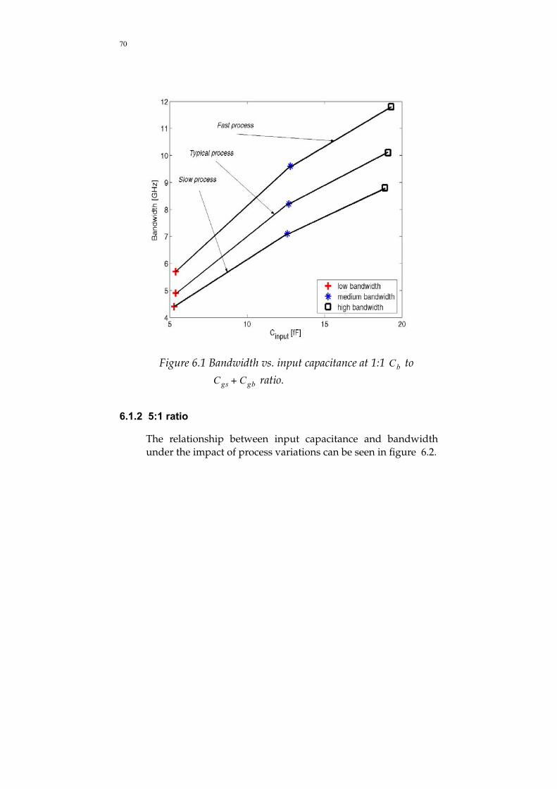
70
Figure 6.1 Bandwidth vs. input capacitance at 1:1 to
ratio.
6.1.2 5:1 ratio
The relationship between input capacitance and bandwidth under the impact of process variations can be seen in figure 6.2.
Cb
Cgs Cgb+

71
Figure 6.2 Bandwidth vs. input capacitance at 5:1 to
ratio.
6.2 Sampling example
The ideal bit-stream that was used in section 3.3.1 was sent over a distributed RLC-line that suffers from capacitive crosstalk from a neighbouring RLC line. The signal is measured when the signal reaches the receiver of the RLC-line.
The 1:1 high bandwidth setup is selected. Typical process setup is used. The simulation setup can be seen in figure 6.3.
Cb
Cgs Cgb+

72
Figure 6.3 Simulation setup for verification.
The tests are performed at different two bit rates of the test sig-nal.
The ideal bitstream is periodic with .
which means that the bits toggle at 3GHz rate, the
signal contains much higher frequency components.
As can be seen in Figure 6.4, the signal at the receiving node is not an ideal one.
Ideal
Bit-stream
Generator
Distributed
RLC-line
Distributed
RLC-line
Capacitive crosstalk
RecieverTransmitter
Bit-stream
Measuring node
f d 750MHz=
f hfc 3GHz=

73
.
Figure 6.4 Signal that is measured in Test 1.
The signal is sampled in two rates that are presented in Table 6.1.
n Output frequency Figure no.
720 MHz 1 30 MHz Figure 6.5
740 MHz 1 10 MHz Figure 6.6
Table 6.1 Four different sampling rates.
f s n,

74
Figure 6.5 Sampled at , .
Most of the waveform has been captured. The small crosstalk glitch in the bottom of the signal has not been detected. The effective sampling frequency was too low, or was too large.
Figure 6.6 Sampled at , .
f s 1, 720MHz= f b 30MHz=
∆t
f s 1, 740MHz= f b 10MHz=

75
At this sampling frequency the effective sampling frequency is high enough, or small enough, to reconstruct the small cross-talk glitch.
6.3 Conclusions
The purpose of this master thesis was to perform a design explo-ration of an on chip measurement circuit and see how much input bandwidth that can be acquired when the capacitive load added to the measuring node is as low as possible.
The circuit is a master and slave track and hold architecture which uses periodic sampling to down convert a high-speed periodic signal to a low frequency that can be brought off chip whitout any attenuation. The work has been done in a 0.13 process at a supply voltage of 1.2V.
The only requirement on the circuit is that it should be able to drive the signal off chip. A capacitance of 2.45pF has been a esti-mation of this load.
This results that is presented shows that the analog behaviour of a high-speed bit stream can be downconverted to a lower fre-quency and be brought off chip. High input bandwidth has been achieved at the cost of relatively low capacitive load.
From the integration tests it is possible to put together a setup that suits application specific requirements. The trade-off that is presented gives an indication of the possibilities of the chosen architecture.
6.4 Personal reflections
During my work with this master thesis I have enhanced my knowledge and understanding of analog design in general, and of track and hold circuits in particular. I have gained experience in many different areas such as sampling theory, design strategy and project management.
I believe that a measuring circuit of this model could be very
∆t
µm

76
useful, especially the setups that have a low input capacitive load. The capacitance that they add to the measuring node is so small that, for instance, a bus driver might not need to take the extra load into consideration when it is designed.
6.4.1 Future improvements
Because of the arrangement of buffers a ~200 mV voltage shift was needed for ultimate performance. This voltage shift was performed in the switch by simply not cancel the clock feed through and channel charge injection. The exact trade-off between gained voltage shift and loss of linearity is not evalu-ated. The effects of using a switch in this way should be investi-gated further.

77
7 REFERENCES
[1] Tektronix “Sampling Oscilloscope Techniques”, Technique Primer 47W-7209
[2] Sune Söderkvist, “Tidsdiskreta Signaler och System”, Tryckeriet Erik Larsson AB, 1994.
[3] R. Lyons “Sampling Bandpass Signals”, http://www.informit.com/articles/article.asp?p=345472&seqNum=3.
[4] Steyskal, H. "Digital Beamforming Antennas", Microwave Journal, January 1987.
[5] G. Hill, "The Benefits of Undersampling" Electronic Design, July 11, 1994.
[6] A. M. Abo, P. R. Gray, “A 1.5-V, 10-bit, 14.3-MS/s CMOS Pipeline Analog-to Digital Converter”, IEEE Journal of Solid-State Circuits, vol. 34, no.5. 599-606, 1999.
[7] M. Takamiya, M. Mizuno, K. Nakamura, “An On-chip 100GHz-Sampling Rate 8-channel Sampling Oscilloscope with Embedded Sampling Clock Gen-erator”, IEEE International Solid-State Circuit Conference, 2002.
[8] K. L. Shepard, Y. Zheng, “On-Chip Oscilloscopes for Non invasive Time-Domain Measurement of Waveforms in Digital Integrated Circuits”, IEEE Transactions on Very Large Scale Integration (VLSI) Systems, vol. 11, no. 3, june 2003.
[9] P. Larsson, C. Svensson, “Measuirng high-bandwidth signals in CMOS cir-cuits”, Electronic Letters, Vol. 29, No. 20 pp. 1761-1762, Sept. 1993.
[10] R. Ho, B. Amrutur, K. Mai, B. Wilburn, T. Mori, M. Horowitz, “Applications of On-Chip Samplers for Test and Measurement of Integrated Circuits”, in Proc. Symposium on VLSI Circuits Digest of Technical Papers, 1998, pp.138-139.

78 Implementering av MSDCT i VHDL
[11] PICO Technology Limited, http://www.picotech.com/applications/oscilloscope_tutorial_swedish.html, January 2005.
[12] N. Forsgren, “Sampling Oscilloscope On-Chip” LiTH-ISY-EX-3301-2003, 2003.
[13] B. Razavi, “Design of Analog CMOS Integrated Circuits”, McGraw-Hill-Education, 2001, ISBN 0-07-238032-2.
[14] D. Jakonis, C. Svensson, “A 1GHz Linearized CMOS Track-and-Hold Cir-cuit”, IEEE International Symposium on Circuits and Systems , Vol. 5, pp. 577-580, May 26-29, 2002.
[15] M. Zin, M.A. Kobayashi, H. Kobayashi, K. Ichimura, J.-I. H. San, Y. Onaya, Y. Kimura, Y. Yuminaka, Y. Sasaki, K. Tanaka, F. Abe, “A High-Speed CMOS Track/Hold Circuit”, Proceedings of the IEEE ICECS, vol.3, pp1709-1712, 1999.
[16] J. M. Rabey, A. Chandrakasan, B Nikolic, “Digital Integrated Circuits, a Des-ing Perspective, second edition”, Prentice Hall, ISBN 0-13-120764-4.
[17] M. Shoji, “Elimination of Process-Dependent Clock Skew in CMOS VLSI”, IEEE Journal of Solid State Circuits, Vol. Sc-21, No.5, October 1986.
[18] E. Säll, “Design of a Low Power, High Performance Track-and-Hold Circuit in a 0.18um CMOS Technology”, LiTH-ISY-EX-3248-2002, 2002.

79
ASIMULATION PARAMETERS
Table A.1 lists the parameters that are unchanged for all integra-tion steps and setups
A.1 Integration master buffer - slave switch - slave buffer
Different setups of the master buffer is presented with three dif-ferent setups of the slave switch.
Transistor W/L [um] Capacitance [fF] Bias
current [mA]
M11 10/0.13 Cload 2450 Ibias3 0.4
M12 103/0.26 Ch2 110
M13 103/0.26
Table A.1 Unchanged parameter values

80
A.1.1 Slave switch setup 1
Table A.2 lists the switch parameters of setup 1.
Table A.3 lists three different optimized setups of the master buffer. The input bandwidth of the master buffer and the gate-drain capacitance of transistor M6 is also presented.
A.1.2 Slave switch setup 2
Table A.4 lists the switch parameters of setup 2.
Transistor W/L [um/um]
M9 10/0.13
M10 12/0.13
Table A.2 Switch parameters of setup 1
width M6
[um]
width M7/M8
[um]
Ibias2 [mA]
M6_cgd [fF]
-3dBBw
[GHz]
100 138.4 3.7 28.1 9.1
150 173 5 46 11.7
250 247 7.6 77.1 14.9
Table A.3 Optimized setups of the master buffer
Transistor W/L [um/um]
M9 7/0.13
M10 8.4/0.13
Table A.4 Switch parameters of setup 2

Table A.3 lists six different optimized setups of the master buffer. The input bandwidth of the master buffer and the gate-drain capacitance of transistor M6 is also presented.
A.1.3 Slave switch setup 3
Table A.6 lists the switch parameters of setup 3.
width M6
[um]
width M7/M8
[um]
Ibias2 [mA]
M6_cgd [fF]
-3dBBw
[GHz]
50 87.4 2.1 15.4 6.3
60 95.7 2.4 18.5 7.3
75 105.4 2.8 23.1 8.7
100 138.4 3.7 28.14 10.7
150 173 5 46 13.5
250 247 7.6 77.11 16.6
Table A.5 Optimized setups of the master buffer
Transistor W/L [um/um]
M9 5/0.13
M10 6/0.13
Table A.6 Switch parameters of setup 3

82
Table A.3 lists three different optimized setups of the master buffer. The input bandwidth of the master buffer and the gate-drain capacitance of transistor M6 is also presented.
A.2 Integration master switch- master buffer - slave switch - slave buffer
Table A.8 lists the parameters that, in addition to parameters in table A.1, are unchanged for setups in this integration step.
Different setups of the master switch is presented for several dif-ferent setups of the master buffer
width M6
[um]
width M7/M8
[um]
Ibias2 [mA]
M6_cgd [fF]
-3dBBw
[GHz]
100 138.4 3.7 28.1 12.7
150 173 5 46 15.4
250 247 7.6 77.1 18.0
Table A.7 Optimized setups of the master buffer
Transistor W/L [um/um]
M9 7/0.13
M10 8.4/0.13
Table A.8 witch parameters in this integration test

A.2.1 Master buffer setup 1
Table A.9 lists the parameters that are unchanged for setup 1.
Table A.10 lists seven different setups of the master switch. The offset voltage produced by the switch for two different input DC-levels are also presented
Transistor W/L [um/um]
Bias current [mA]
M6 50/0.13 Ibias2 2.1
M7/M8 87.44/0.25
Table A.9 Master buffer parameters for setup 1
WidthM5 [um] Ch [fF]
|Offset volt| [mV]
dc=250 dc=650
10 1 219.6 199.4
15 10 201 190.8
20 20 195.8 197
25 30 191.9 200.6
30 30 206.7 226.5
35 45 193.5 214
45 60 193.3 221.8
Table A.10 Different setups of master switch in setup 1

84
A.2.2 Master buffer setup 2
Table A.11 lists the parameters that are unchanged for setup 2.
Table A.12 lists seven different setups of the master switch. The offset voltage produced by the switch for two different input DC-levels are also presented
Transistor W/L [um/um]
Bias current [mA]
M6 60/0.13 Ibias2 2.4
M7/M8 95.7/0.25
Table A.11 Master buffer parameters for setup 2
WidthM5 [um] Ch [fF]
|Offset volt| [mV]
dc=250 dc=650
12 1 203.7 177
17 10 201.2 191.7
23 20 200 203.5
27 30 192.5 200.5
37 45 193.6 213.2
45 60 190 214.7
12 1 203.7 177
Table A.12 Different setups of master switch in setup 2

A.2.3 Master buffer setup 3
Table A.13 lists the parameters that are unchanged for setup 3.
Table A.14 lists seven different setups of the master switch. The offset voltage produced by the switch for two different input DC-levels are also presented
Transistor W/L [um/um]
Bias current [mA]
M6 60/0.13 Ibias2 2.4
M7/M8 95.7/0.25
Table A.13 Master buffer parameters for setup 3
WidthM5 [um] Ch [fF]
|Offset volt| [mV]
dc=250 dc=650
12 1 203.7 177
17 10 201.2 191.7
23 20 200 203.5
27 30 192.5 200.5
37 45 193.6 213.2
45 60 190 214.7
12 1 203.7 177
Table A.14 Different setups of master switch in setup 3

86
A.2.4 Master buffer setup 4
Table A.15 lists the parameters that are unchanged for setup 4.
Table A.16 lists seven different setups of the master switch. The offset voltage produced by the switch for two different input DC-levels are also presented
A.2.5 Master buffer setup 5
Table A.17 lists the parameters that are unchanged for setup 5.
Transistor W/L [um/um]
Bias current [mA]
M6 75/0.13 Ibias2 2.8
M7/M8 105.4/0.25
Table A.15 Master buffer parameters for setup 4
WidthM5 [um] Ch [fF]
|Offset volt| [mV]
dc=250 dc=650
15 1 203.9 182.1
17 1 214.9 200.3
25 20 196.7 198
30 30 193 200.8
45 60 185.2 205.2
Table A.16 Different setups of master switch in setup 4
Transistor W/L [um/um]
Bias current [mA]
M6 100/0.13 Ibias2 3.7
Table A.17 Master buffer parameters for setup 5

Table A.18 lists seven different setups of the master switch. The offset voltage produced by the switch for two different input DC-levels are also presented
A.2.6 Master buffer setup 6
Table A.19 lists the parameters that are unchanged for setup 6.
Table A.20 lists seven different setups of the master switch. The offset voltage produced by the switch for two different input
M7/M8 138.4/0.25
WidthM5 [um] Ch [fF]
|Offset volt| [mV]
dc=250 dc=650
15 1 177.8 145.3
17 1 194 168.9
30 30 180.7 177.9
45 50 187.8 202.2
60 75 185.8 210.3
Table A.18 Different setups of master switch in setup 5
Transistor W/L [um/um]
Bias current [mA]
M6 150/0.13 Ibias2 5
M7/M8 173./0.25
Table A.19 Master buffer parameters for setup 6
Transistor W/L [um/um]
Bias current [mA]
Table A.17 Master buffer parameters for setup 5

88
DC-levels are also presented.
WidthM5 [um] Ch [fF]
|Offset volt| [mV]
dc=250 dc=650
23 1 179 154
50 30 200.5 215
50 50 181 189.4
60 75 174.3 188.4
65 75 180.1 199.1
Table A.20 Different setups of master switch in setup 6

På svenska
Detta dokument hålls tillgängligt på Internet – eller dess framtida ersättare – under en längre tid från publiceringsdatum under förutsättning att inga extra-ordinära omständigheter uppstår.
Tillgång till dokumentet innebär tillstånd för var och en att läsa, ladda ner, skriva ut enstaka kopior för enskilt bruk och att använda det oförändrat för ick-ekommersiell forskning och för undervisning. Överföring av upphovsrätten vid en senare tidpunkt kan inte upphäva detta tillstånd. All annan användning av dokumentet kräver upphovsmannens medgivande. För att garantera äktheten, säkerheten och tillgängligheten finns det lösningar av teknisk och administrativ art.Upphovsmannens ideella rätt innefattar rätt att bli nämnd som upphovsman i den omfattning som god sed kräver vid användning av dokumentet på ovan beskrivna sätt samt skydd mot att dokumentet ändras eller presenteras i sådan form eller i sådant sammanhang som är kränkande för upphovsmannens litterära eller konst-närliga anseende eller egenart.
För ytterligare information om Linköping University Electronic Press se för-lagets hemsida http://www.ep.liu.se/
In English
The publishers will keep this document online on the Internet - or its possible replacement - for a considerable time from the date of publication barring excep-tional circumstances.
The online availability of the document implies a permanent permission for anyone to read, to download, to print out single copies for your own use and to use it unchanged for any non-commercial research and educational purpose. Sub-sequent transfers of copyright cannot revoke this permission. All other uses of the document are conditional on the consent of the copyright owner. The pub-lisher has taken technical and administrative measures to assure authenticity, security and accessibility.
According to intellectual property law the author has the right to be men-tioned when his/her work is accessed as described above and to be protected against infringement.
For additional information about the Linköping University Electronic Press and its procedures for publication and for assurance of document integrity, please refer to its WWW home page: http://www.ep.liu.se/
© Arvid Stridfelt