high speed digital design
TRANSCRIPT

HIGH-SPEED DIGITAL DESIGN
A Handbook of Black Magic
HOWARD W. JOHNSON, PH.D. Olympic Technology Group, Inc.
MARTIN GRAHAM, PH.D. University of California at Berkeley
For book and bookstore information
http://www.prenhall.com gopher to gopher.prenhall.com
Prentice Hall PTR, Englewood Cliffs, New Jersey 07632

Contents
Preface ix
1 Fundamentals 1
1.1 Frequency and Time 1 1.2 Time and Distance 6 1.3 Lumped Versus Distributed Systems 7 1.4 A Note About 3 dB and RMS Frequencies 8 1.5 Four Kinds of Reactance 10 1.6 Ordinary Capacitance 11 1.7 Ordinary Inductance 17 1.8 A Better Method for Estimating Decay Time 22 1.9 Mutual Capacitance 25
1.10 Mutual Inductance 29
2 High-Speed Properties of Logic Gates 37
2.1 Historical Development of a Very Old Digital Technology 37
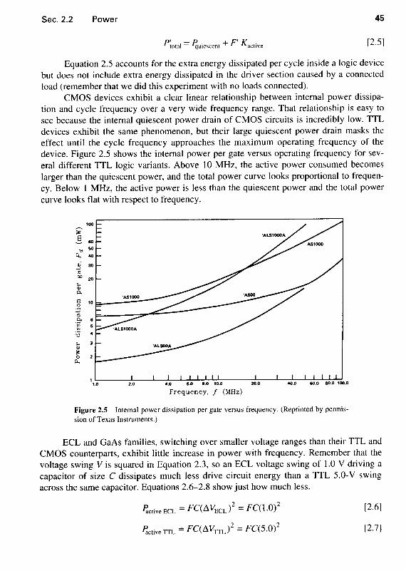
2.2 Power 39 2.3 Speed 59 2.4 Packaging 66
v

vi
3 Measurement Techniques 83
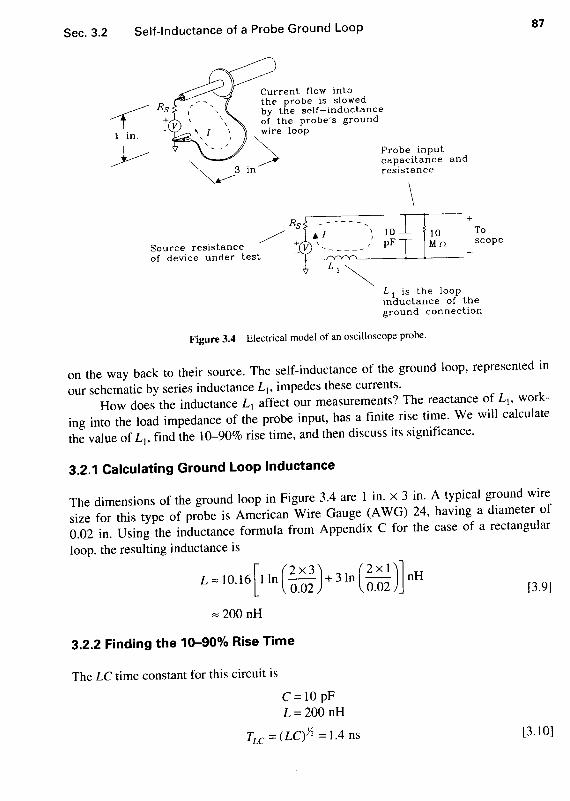
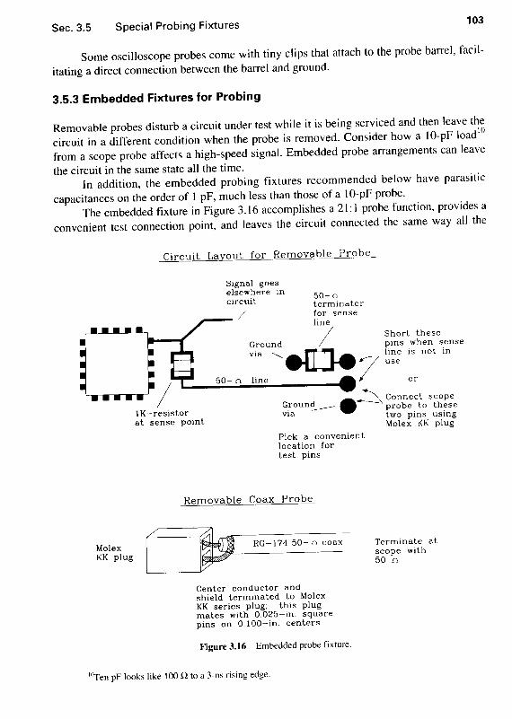
3.1 Rise Time and Bandwidth of Oscilloscope Probes 83 3.2 Self-inductance of a Probe Ground Loop 86 3.3 Spurious Signal Pickup from Probe Ground Loops 92 3.4 How Probes Load Down a Circuit 95 3.5 Special Probing Fixtures 98 3.6 Avoiding Pickup from Probe Shield Currents 104 3.7 Viewing a Serial Data Transmission System 108 3.8 Slowing Down the System Clock 110 3.9 Observing Crosstalk 111
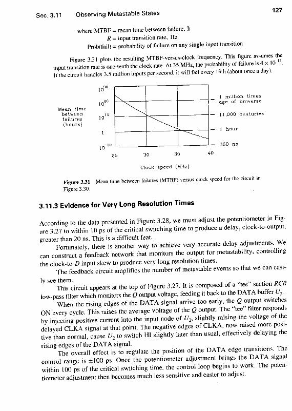
3.10 Measuring Operating Margins 113 3.11 Observing Metastable States 120
4 Transmission Lines 133
4.1 Shortcomings of Ordinary Point-to-Point Wiring 133 4.2 Infinite Uniform Transmission Line 140 4.3 Effects of Source and Load Impedance 160 4.4 Special Transmission Line Cases 167 4.5 Line Impedance and Propagation Delay 178
5 Ground Planes and Layer Stacking 189
5.1 5.2 5.3 5.4 5.5 5.6 5.7 5.8
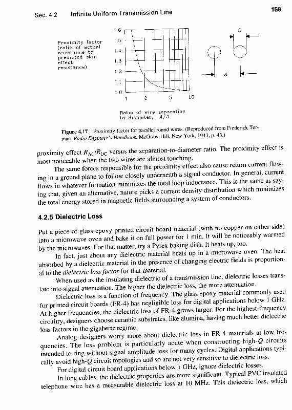
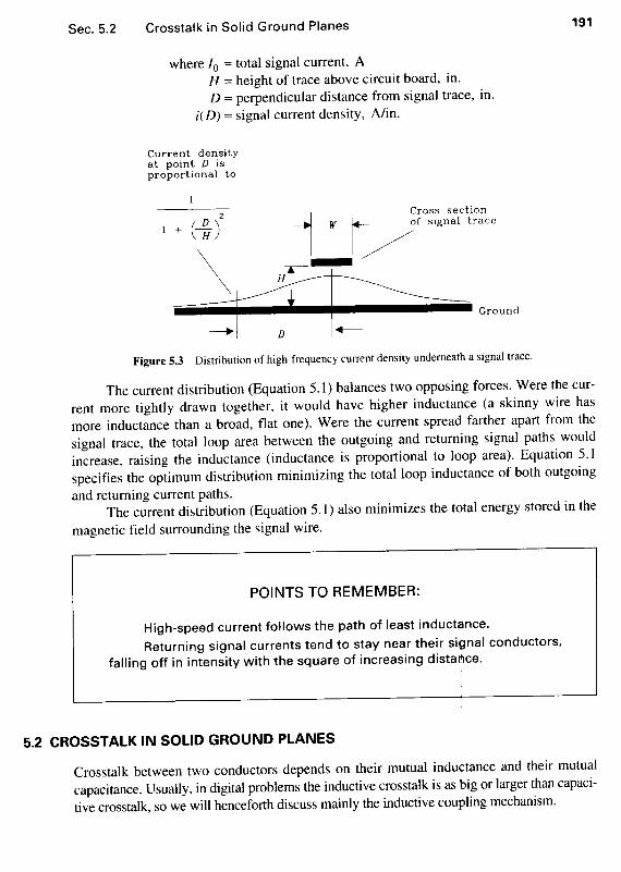
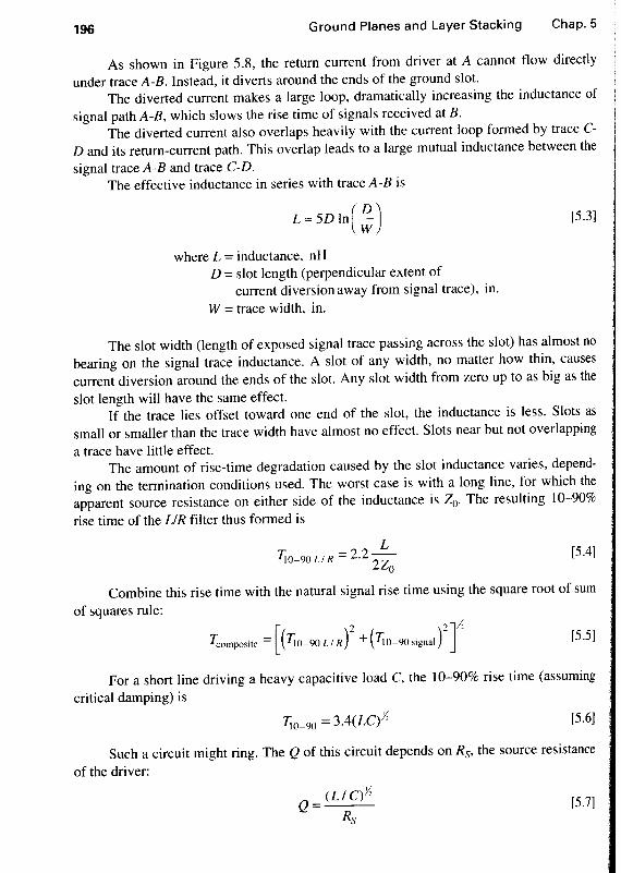
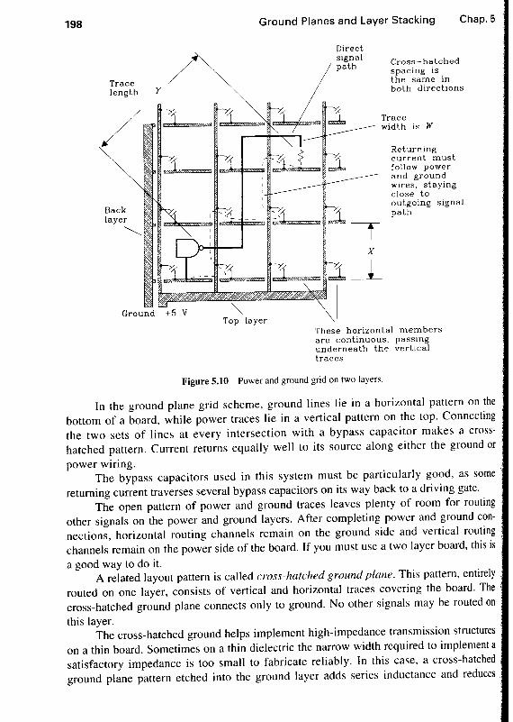
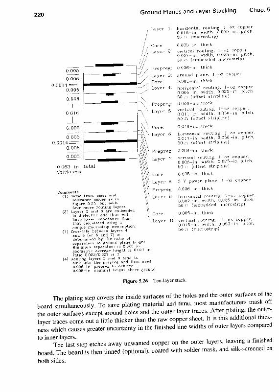
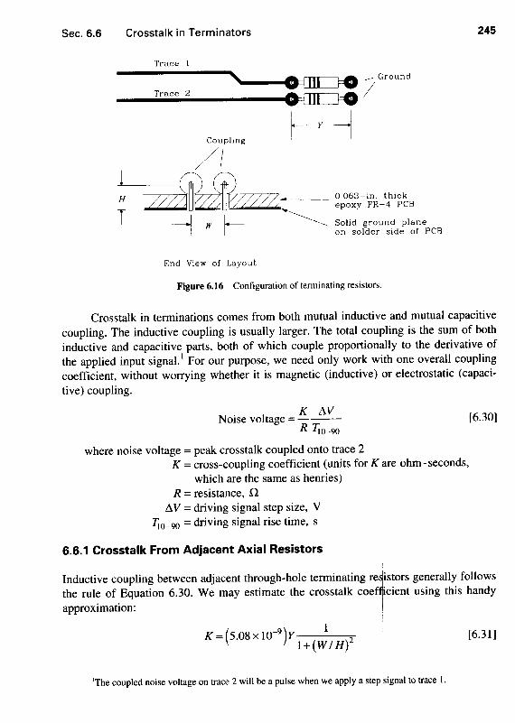
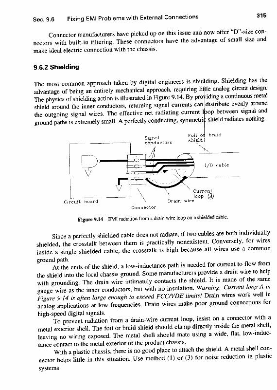
High-Speed Current Follows the Path of Least Inductance Crosstalk in Solid Ground Planes 191 Crosstalk in Slotted Ground Planes 194 Crosstalk in Cross-Hatched Ground Planes Crosstalk with Power and Ground Fingers Guard Traces 201 Near-End and Far-End Crosstalk 204 How to Stack Printed Circuit Board Layers
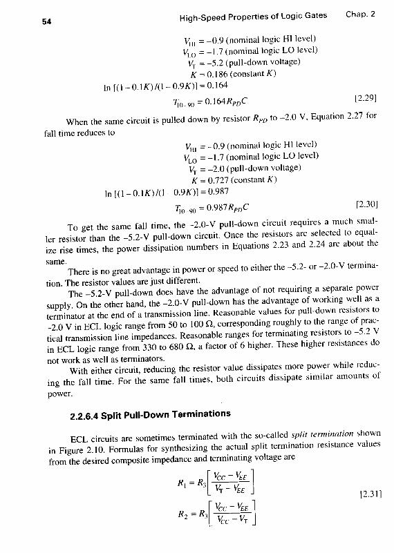
6 Terminations 223
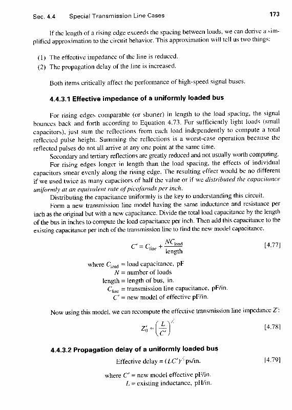
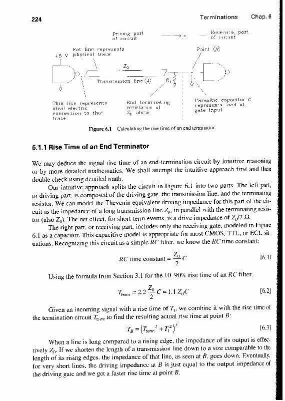
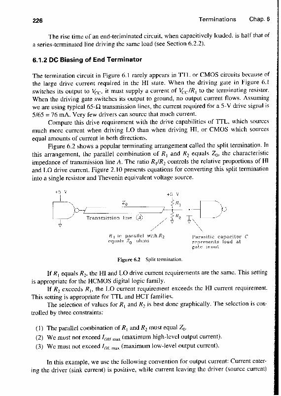
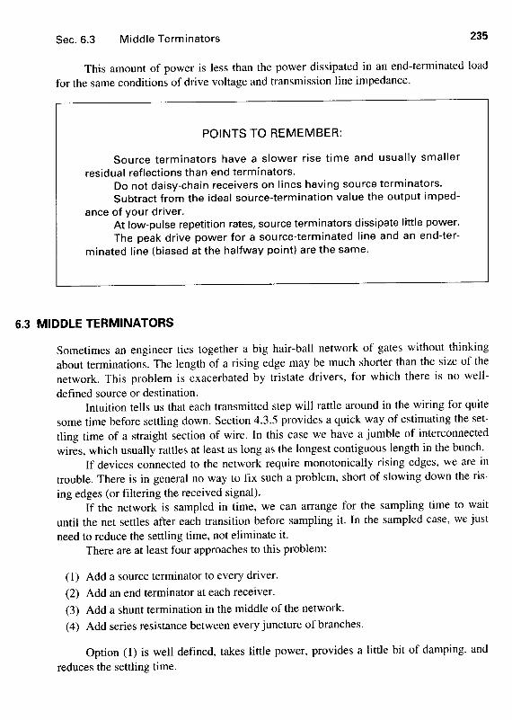
6.1 End Terminators 223 6.2 Source Terminators 231 6.3 Middle Terminators 235 6.4 AC Biasing for End Terminators 236 6.5 Resistor Selection 239 6.6 Crosstalk in Terminators 244
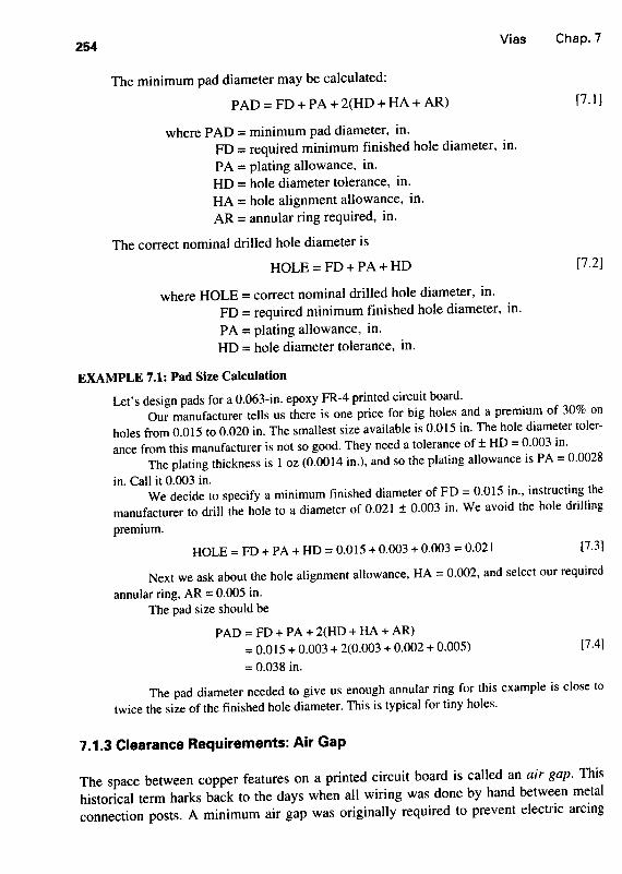
7 Vias 249
7.1 Mechanical Properties of Vias 249 7.2 Capacitance of Vias 257 7.3 Inductance of Vias 258
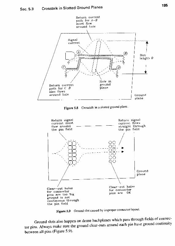
197 199
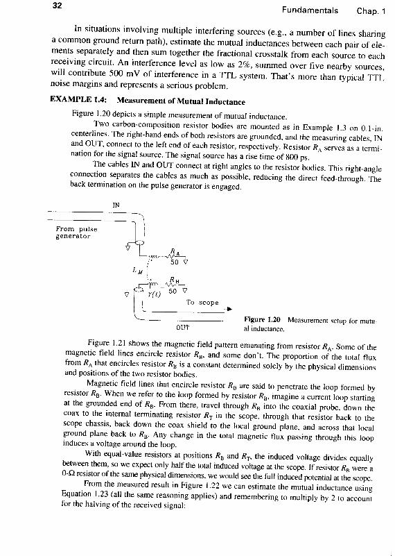
212
7.4 Return Current and Its Relation to Vias 260
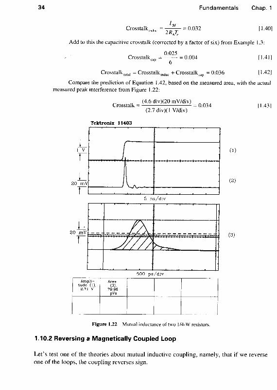
Contents
189

Contents vii
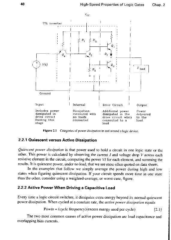
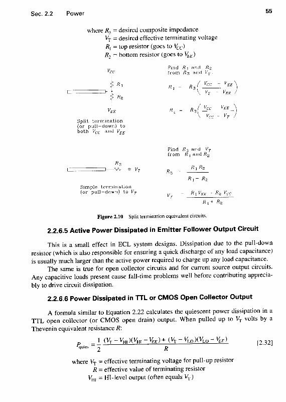
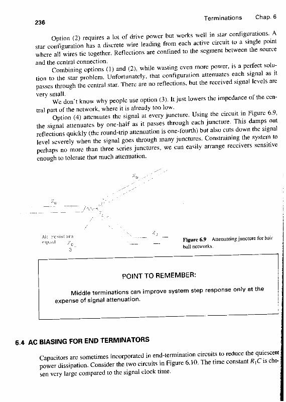
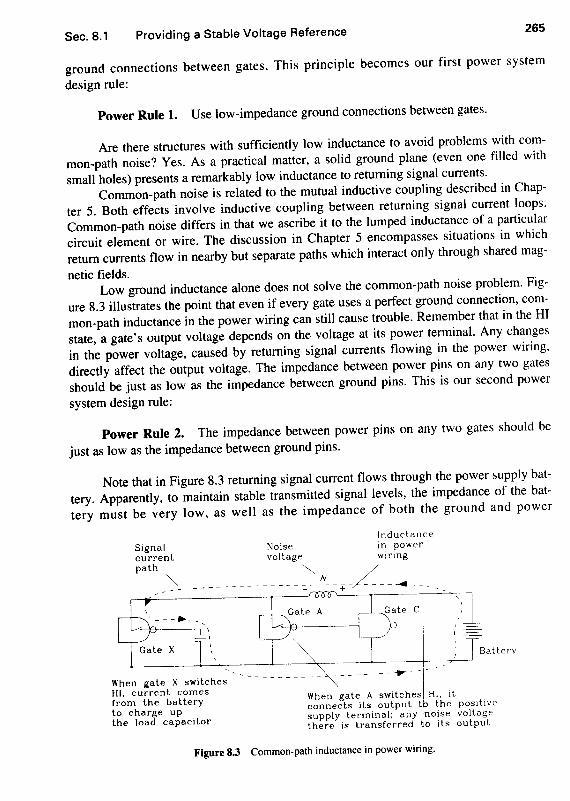
8 Power Systems 263
8.1 Providing a Stable Voltage Reference 263 8.2 Distributing Uniform Voltage 268 8.3 Everyday Distribution Problems 279 8.4 Choosing a Bypass Capacitor 281
9 Connectors 295
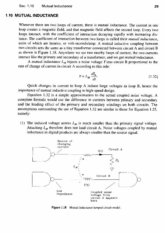
9.1 Mutual Inductance-How Connectors Create Crosstalk 295
9.2 Series Inductance-How Connectors Create EMI 300 9.3 Parasitic Capacitance-Using Connectors on a
Multidrop Bus 305 9.4 Measuring Coupling in a Connector 309 9.5 Continuity of Ground Underneath a Connector 312 9.6 Fixing EMI Problems with External Connections 314 9.7 Special Connectors for High-Speed Applications 316 9.8 Differential Signaling Through a Connector 319 9.9 Power Handling Features of Connectors 321
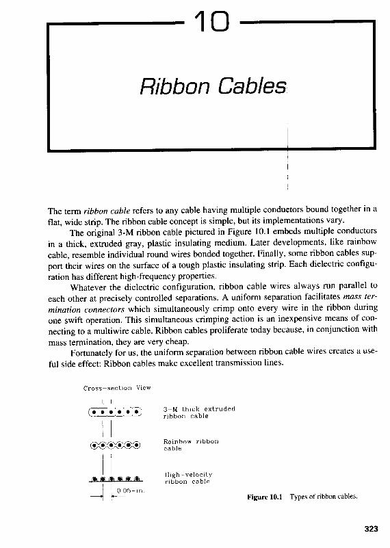
10 Ribbon Cables 323
10.1 Ribbon Cable Signal Propagation 324 10.2 Ribbon Cable Crosstalk 329 10.3 Ribbon Cable Connectors 336 10.4 Ribbon Cable EMI 338
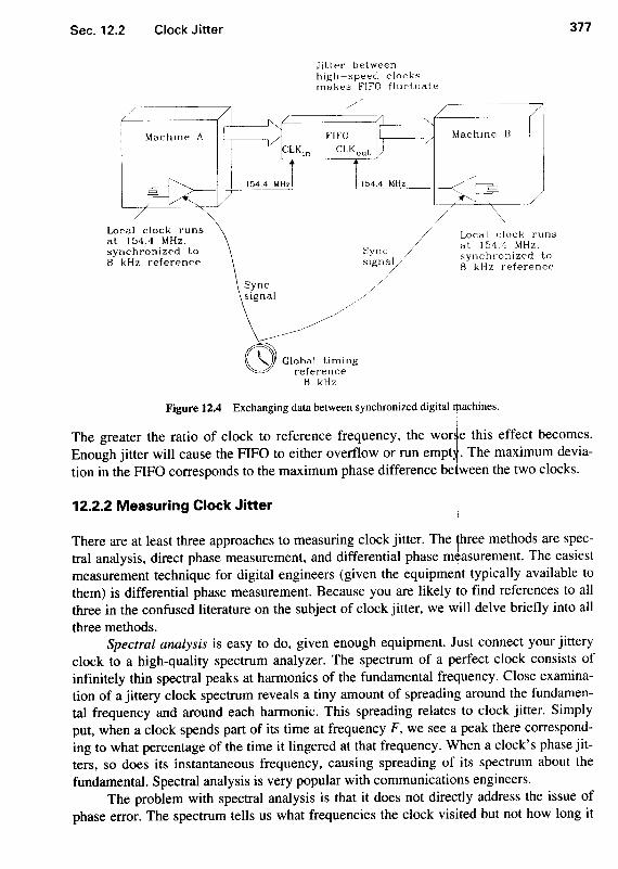
11 Clock Distribution 341
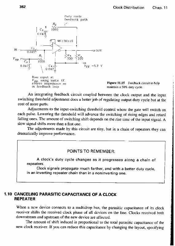
11.1 Timing Margin 341 11.2 Clock Skew 343 11.3 Using Low-Impedance Drivers 346 11.4 Using Low-Impedance Clock Distribution Lines 348 11.5 Source Termination of Multiple Clock Lines 350 11.6 Controlling Crosstalk on Clock Lines 352 11.7 Delay Adjustments 353 11.8 Differential Distribution 360 11.9 Clock Signal Duty Cycle 361
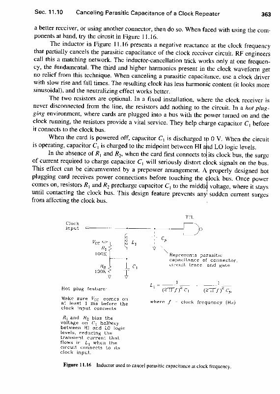
11.10 Canceling Parasitic Capacitance of a Clock Repeater 362
11.11 Decoupling Clock Receivers from the Clock Bus 364
12 Clock Oscillators 367
12.1 Using Canned Clock Oscillators 367 12.2 Clock Jitter 376

viii Contents
Collected References 385
A Points to Remember 389
B Calculation of Rise Time 399
C MathCad Formulas 409
Index 441
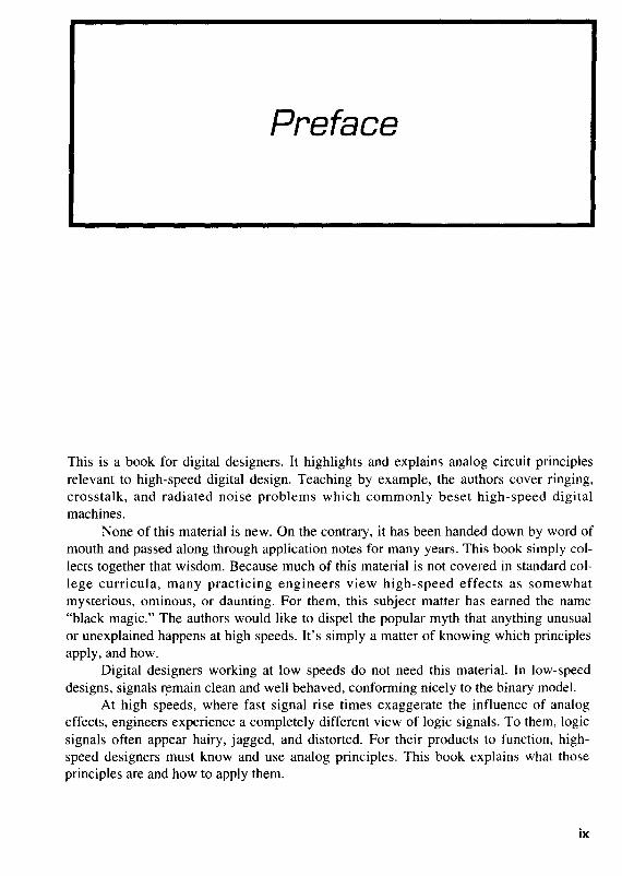
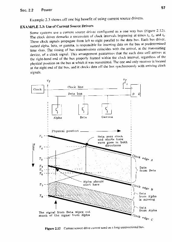
Preface
This is a book for digital designers. It highlights and explains analog circuit principles relevant to high-speed digital design. Teaching by example, the authors cover ringing, crosstalk, and radiated noise problems which commonly beset high-speed digital machines.
None of this material is new. On the contrary, it has been handed down by word of mouth and passed along through application notes for many years. This book simply collects together that wisdom. Because much of this material is not covered in standard college curricula, many practicing engineers view high-speed effects as somewhat mysterious, ominous, or daunting. For them, this subject matter has earned the name "black magic." The authors would like to dispel the popular myth that anything unusual or unexplained happens at high speeds. It's simply a matter of knowing which principles apply, and how.
Digital designers working at low speeds do not need this material. In low-speed designs, signals r~main clean and well behaved, conforming nicely to the binary model.
At high speeds, where fast signal rise times exaggerate the influence of analog effects, engineers experience a completely different view of logic signals. To them, logic signals often appear hairy, jagged, and distorted. For their products to function, highspeed designers must know and use analog principles. This book explains what those principles are and how to apply them.
ix

x Preface
Readers without the benefit of formal training in analog circuit theory can use and apply the formulas and examples in this book. Readers who have completed a first year class in introductory linear circuit theory may comprehend this material at a deeper level.
Chapters 1-3 introduce analog circuit terminology, the high-speed properties of logic gates, and standard high-speed measurement techniques, respectively. These three chapters form the core of the book and should be included in any serious study of highspeed logic design.
The remaining chapters, 4-12, each treat specialized topics in high-speed logic design and may be studied in any order.
Appendix A collects highlights from each section, listing the most important ideas and concepts presented. It can be used as a checklist for system design or as an index to the text when facing a difficult problem.
Appendix B details the mathematical assumptions behind various forms of rise time measurement. This section helps relate results given in this book to other sources and standards of nomenclature.
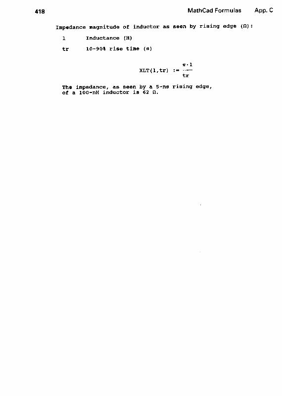
Appendix C lists standard formulas for computing the resistance, capacitance, and inductance of physical structures. These formulas have been implemented in MathCad and are available from the authors in magnetic form.
KNOWLEDGMENTS
Many people have contributed to this book, and we would like to thank them all. To our teachers, employers, fellow workers, clients, customers, and students, we thank you for motivating us to learn, for showing us problems we could not solve, and for occasionally humbling us when we acted like we knew too much.
The authors would like to thank individually the following people for the generous contributions they have made to the writing of this book: For meticulously reviewing the text and for offering many, many good suggestions we thank Dan Nitzan, Jim Pomerene, Joel Cyprus, Ernie Kim, Tim Ryan, and Charlie Adams.
For her efficient and cheerful assistance in preparing the figures, we thank our assistant, Pamela Moore.
Dr. Johnson would like to thank the former officers and management of ROLM corporation, particularly Ken ashman, Bob Maxfield, and Gibson Anderson for giving him a big head start in the electronics industry.
For having a profound effect on his approach to problem-solving, and on his teaching career, Martin Graham wishes to acknowledge his mentor of long ago, Professor William McLean.
Of course, we owe a big debt of gratitude to Tektronix for loaning us a Tek 11403 digitizing oscilloscope. Their scope produced all the fine waveform displays you see in the book. Each waveform was captured, stored in memory, and then plotted directly to hard copy. Thank you, Leo Chamberlain and Jim McGoffin.
Last, and certainly not least, to our wives, Elisabeth and Selma, for their devotion and untiring support, we express our heartfelt appreciation and thanks.

Preface xi
, NOTE TO THE READER
To those of you who will undoubtedly report the discovery of technical errors in the manuscript, thank you for your attention and for taking the time to write to us about it. The authors will personally send a certificate of appreciation to the first person to document each substantive technical error in the book. Please send your comments to:
Howard W. Johnson, Ph.D. Olympic Technology Group, Inc. 16541 Redmond Way, Suite 264 Redmond, W A 98052

High-Speed Digital Design

1
Fundamentals
High-speed digital design, in contrast to digital design at low speeds, emphasizes the behavior of passive circuit elements. These passive elements may include the wires, circuit boards, and integrated-circuit packages that make up a digital product. At low speeds, passive circuit elements are just part of a product's packaging. At higher speeds they directly affect electrical performance.
High-speed digital design studies how passive circuit elements affect signal propagation (ringing and reflections), interaction between signals (crosstalk), and interactions with the natural world (electromagnetic interference).
Let's begin our study of high-speed digital design by reviewing some relationships among frequency, time, and distance.
1.1 FREQUENCY AND TIME
At low frequencies, an ordinary wire will effectively short together two circuits. This is not the case at high frequencies. At high frequencies, only a wide, flat object can short two circuits. The same wire which is so effective at low frequencies has too much inductance to function as a short at high frequencies. We might use it as a high-frequency inductor but not as a high-frequency short circuit.
Is this a common occurrence? Do circuit elements that work in one frequency range normally not work in a different frequency range? Are electrical parameters really that frequency-sensitive?
Yes. Drawn on a log-frequency scale, few electrical parameters remain constant across more than 10 or certainly 20 frequency decades. For every electrical parameter, we must consider the frequency range over which that parameter is valid.
Exploring further this idea of wide frequency ranges, let's first consider very low frequencies, corresponding to extremely long intervals of time. Then we will see what happens at very high frequencies.
1
2 Fundamentals Chap. 1
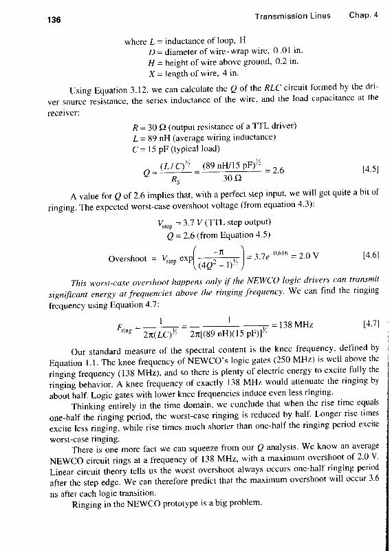
A sine wave of 10- 12 Hz completes a cycle only once every 30.000 years. At 10-12 Hz, a sine wave of transistor-transistor logic (TTL) proportions varies less than II.LV in a day. That is a very low frequency indeed, but not quite zero.
Any experiment involving semiconductors at a frequency of 10-12 Hz will (eventually) reveal that they do not function. It takes so long to run an experiment at 10-12 Hz that the circuits turn to dust. Viewed on a very long time scale, integrated circuits are nothing but tiny lumps of oxidized silicon.
Given this unexpected behavior at 10-12 Hz, what do you suppose will happen at the opposite extreme. perhaps 10+12 Hz?
As we move radically up in frequency, to very short intervals of time, other electrical parameter changes occur. For example, the electric resistance of a short ground wire measuring 0.01 Q at 1 kHz increases, due to the skin effect, to 1.0 Q at I gHz. Not only that, it acquires 50 Q of inductive reactance!
Big changes in performance always occur in electric circuit elements when pushed to the upper end of their operating frequency range.
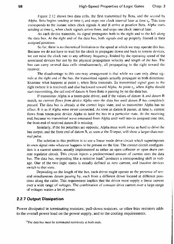
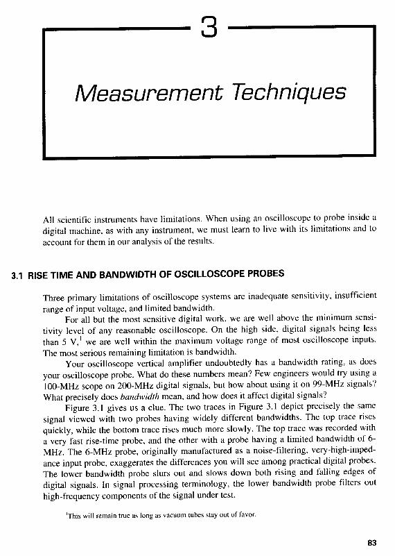
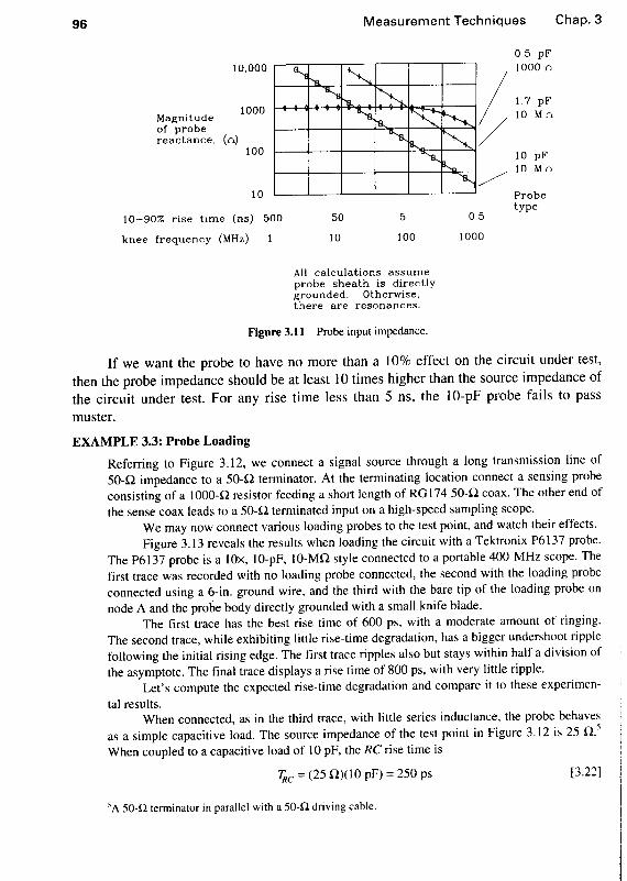
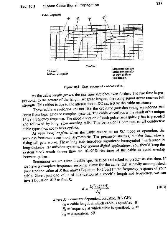
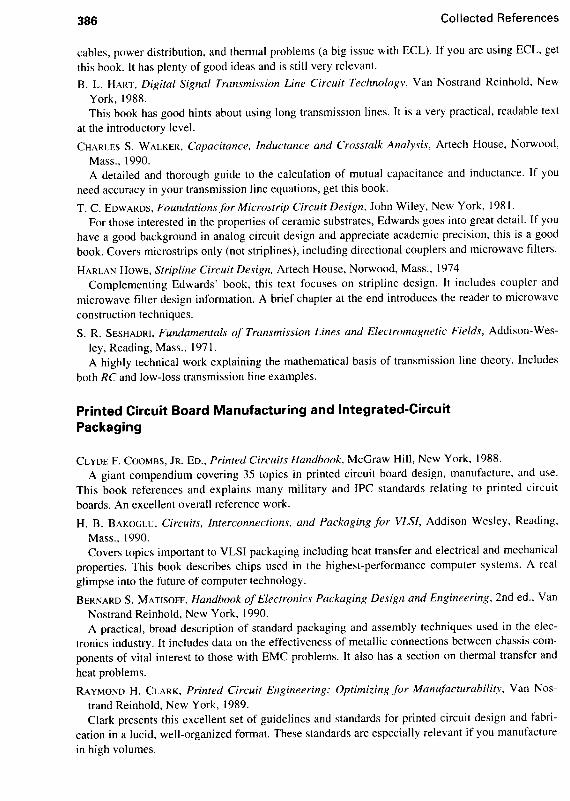
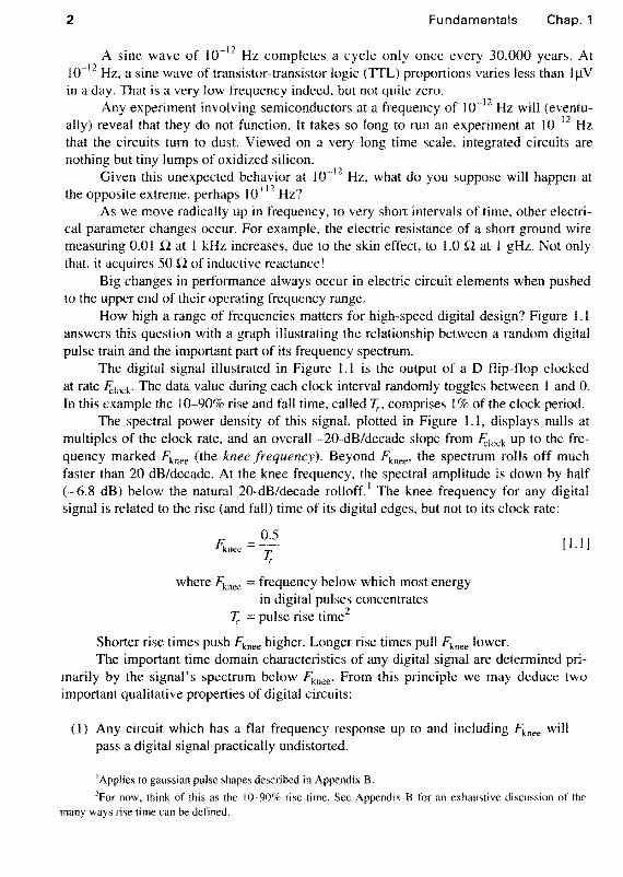
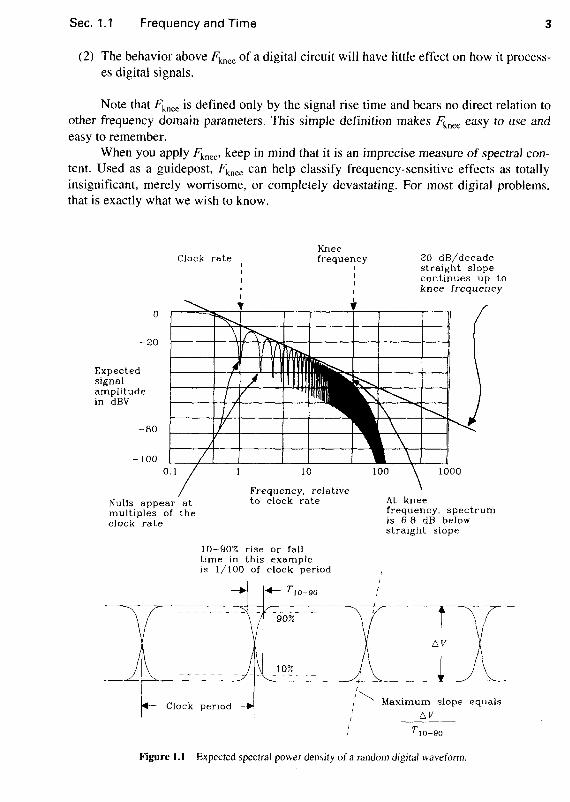
How high a range of frequencies matters for high-speed digital design? Figure 1.1 answers this question with a graph illustrating the relationship between a random digital pulse train and the important part of its frequency spectrum.
The digital signal illustrated in Figure 1.1 is the output of a D flip-flop clocked at rate J;:lock' The data value during each clock interval randomly toggles between I and O. In this example the 10-90% rise and fall time, called T,., comprises 1 % of the clock period.
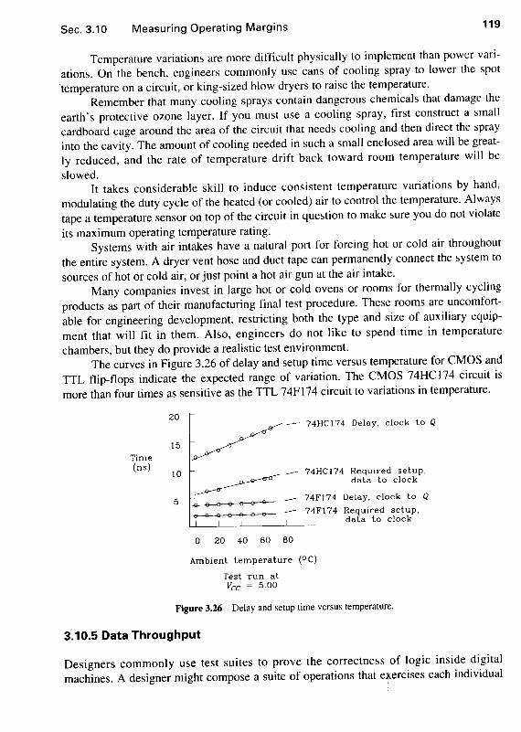
The spectral power density of this signal, plotted in Figure 1.1, displays nulls at multiples of the clock rate, and an overall -20-dB/decade slope from J;:lock up to the frequency marked Fknee (the knee frequency). Beyond Fknee , the spectrum rolls off much faster than 20 dB/decade. At the knee frequency, the spectral amplitude is down by half (-6.8 dB) below the natural 20-dB/decade roIloff.1 The knee frequency for any digital signal is related to the rise (and fall) time of its digital edges, but not to its clock rate:
0.5
1; where Fknee = frequency below which most energy
in digital pulses concentrates 7; pulse rise time2
Shorter rise times push Fknee higher. Longer rise times pull Fknee lower.
[ I.IJ
The important time domain characteristics of any digital signal are determined primarily by the signal's spectrum below finee. From this principle we may deduce two important qualitative properties of digital circuits:
(I) Any circuit which has a flat frequency response up to and including Fknee will pass a digital signal practically undistorted.
I Applies to gaussian pulse shapes described in Appendix B.
"For now, think of this as the 10--90% rise time. See Appendix B for an exhaustive discussion of the many ways rise time can be defined.
Sec. 1.1 Frequency and Time 3
(2) The behavior above Fknee of a digital circuit will have little effect on how it processes digital signals.
Note that Fknee is defined only by the signal rise time and bears no direct relation to other frequency domain parameters. This simple definition makes Fknee easy to use and
easy to remember. When you apply Fknw keep in mind that it is an imprecise measure of spectral con
tent. Used as a guidepost, Fknee can help classify frequency-sensitive effects as totally insignificant, merely worrisome, or completely devastating. For most digital problems, that is exactly what we wish to know.
Clock rate Knee frequency
I
o
-20
Expected signal amplitude in dBV
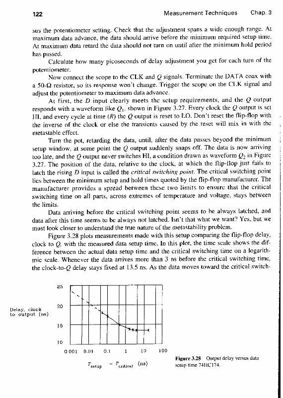
-80
-100 0.1
Nulls appear at multiples of the clock rate
10
Frequency, relative to clock rate
10-905;: rise or fall time in this example is 1/100 of clock period
---. ..f-- T 10 - 90
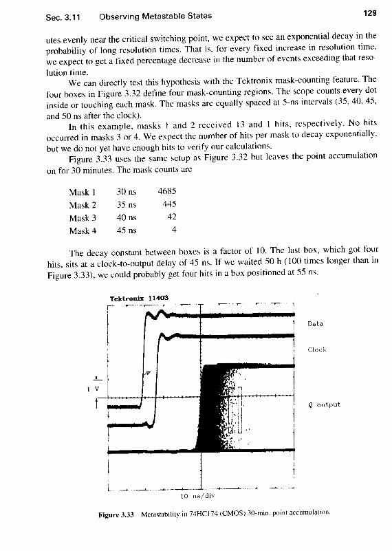
90%
10%
I I
I
20 dB/decade straight slope continues up to knee frequency
1000
At knee frequency, spectrum is 6.8 dB below straight slope
I~ I Maximum slope equals Clock period
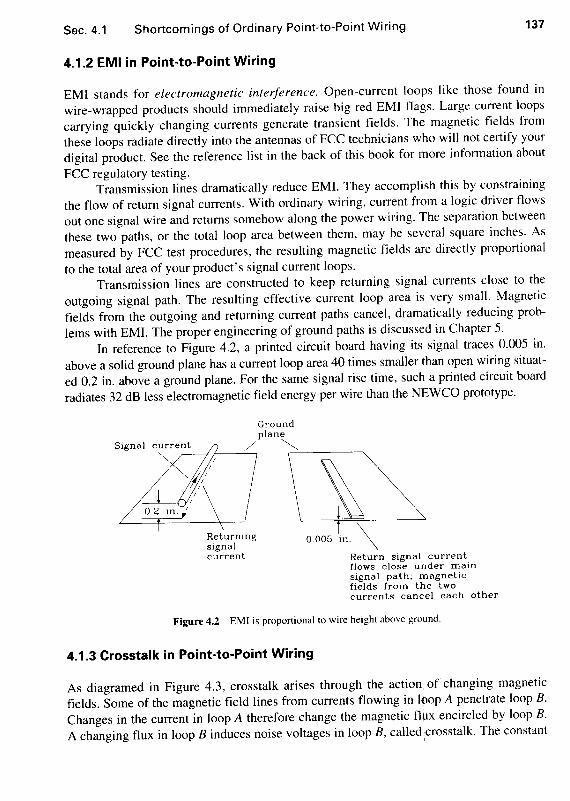
I
I
I
I 6V
Figure 1.1 Expected spectral power density of a random digital waveform.
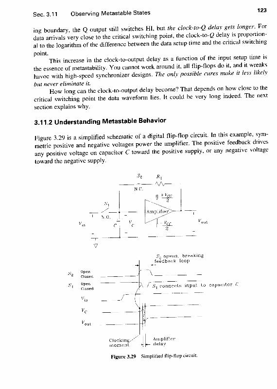
4 Fundamentals Chap. 1
Of course, Fknee has limitations. Fknee cannot make precise predictions about system behavior. It doesn't even define precisely how to measure rise time! It is no substitute for full-blown Fourier analysis. It can't predict electromagnetic emissions, whose properties depend on the detailed spectral behavior at frequencies well above Fknee •
At the same time, for digital signals, Fknee quickly relates time to frequency in a practical and useful manner. We will use Fknee throughout this book as the practical upper bound on the spectral content of digital signals. Appendix B contains additional information, for those interested, about various measures of rise time and frequency.
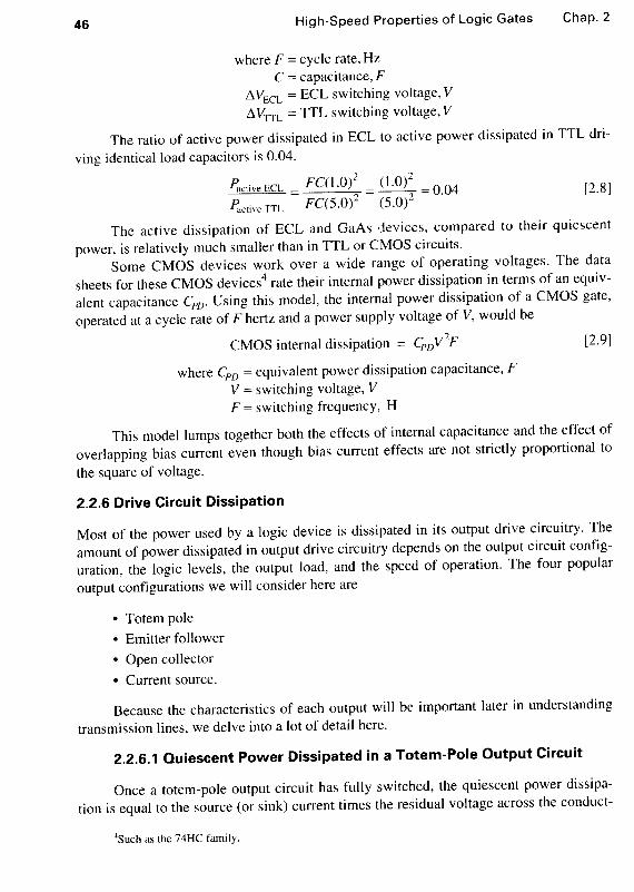
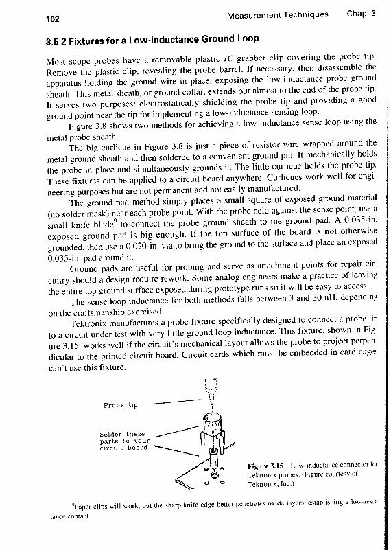
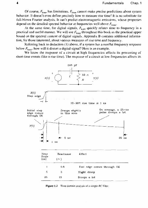
Referring back to deduction (1) above, if a system has a nonflat frequency response below Fknee, how will it distort a digital signal? Here is an example.
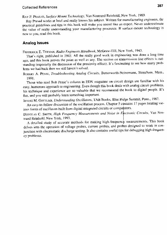
We know the response of a circuit at high frequencies affects its processing of short-time events (like a rise time). The response of a circuit at low frequencies affects its
X(t) Step
500 pF
+ y(t)
1 ns
Initial step Droops slightly On average, a 25-ns pulse droops a lot edge comes in this area
thrOU~nOKI ~ / l y(t) ~-------------l.
~ l- 1 n,' 5 n' 25 "'
Time Reactance Effect Scale (ns) (n)
0.6 Fast edge comes through OK
5 3 Slight droop
25 15 Droops a lot
Figure 1.2 Time domain analysis of a simple RC filter.

Sec. 1.1 Frequency and Time 5
processing of longer-term events (such as a long, steady pulse). Figure 1.2 shows a circuit having different characteristics at high and low frequencies. This circuit passes high-frequency events (the rising edge) but does not pass low-frequency events (the long, steady part).
Let's start our analysis of Figure 1.2 at one particular frequency: F knee. At the frequency Fknee> capacitor C has a reactance (i.e., impedance magnitude) of 1/C21tFknee .
We can calculate the reactance using this formula or substitute rise time for Fknee:
1 Tr Xc == = 1tC == 0.60
21tF/<nee C
where 1', == rise time of step input, s Fknee == highest frequency in step input, Hz
C == capacitance, F
[1.2]
Equation 1.2 shows how to estimate the reactance of a capacitor using either the knee frequency or rise time.
A 0.6-0 reactance acts as a virtual short in the circuit in Figure 1.2. The full amplitude of the leading edge, corresponding to a frequency of Fknee , will come blasting straight through the capacitor.
Over a time interval of 25 ns, corresponding roughly to a frequency of 20 MHz, the capacitive reactance increases to 15 0, causing the coupled signal to droop noticeably.
POINTS TO REMEMBER:
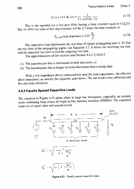
The response of a circuit at high frequencies affects its processing of short-time events.
The response of a circuit at low frequencies affects its processing of long-term events.
cy: Most energy in digital pulses concentrates below the knee frequen-
0.5 Fknee == T
r
The behavior of a circuit at the knee frequency determines its processing of a step edge.
The behavior of a circuit at frequencies above Fknee hardly affects digital performance.

6 Fundamentals Chap. 1
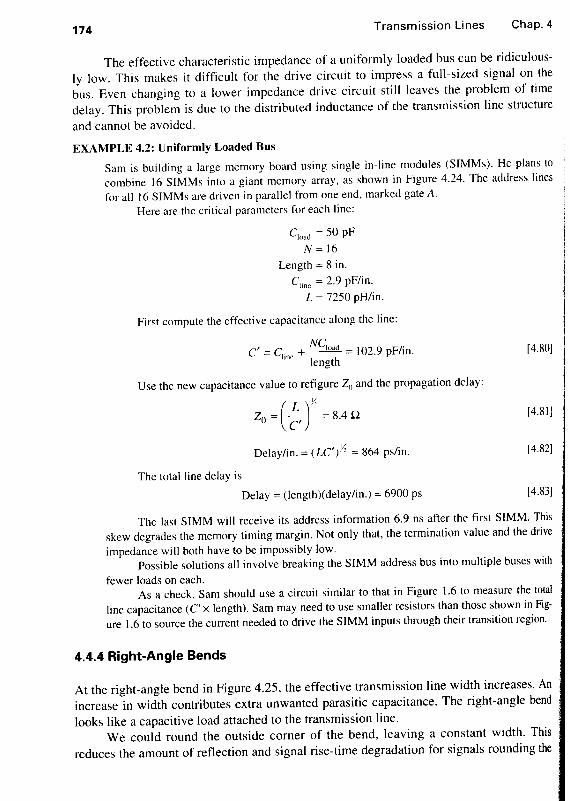
1.2 TIME AND DISTANCE
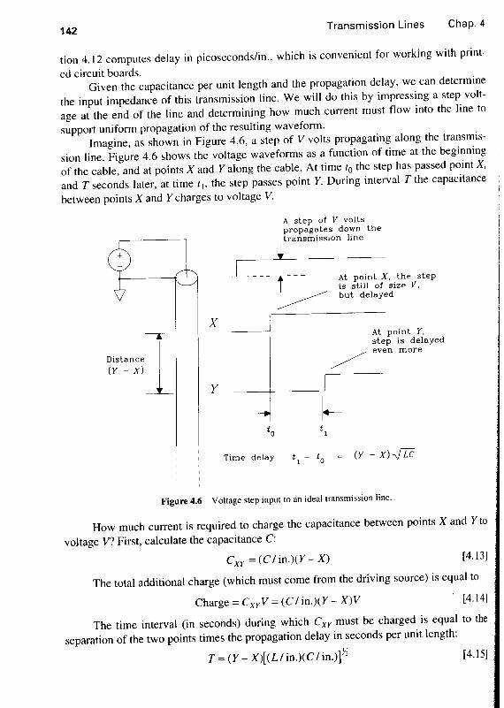
Electrical signals in conducting wires, or conducting circuit traces, propagate at a speed dependent on the surrounding medium. Propagation delay is measured in units of picoseconds per inch. Propagation delay is the inverse of propagation velocity (also called propagation speed), which is measured in inches per picosecond.
TABLE 1.1 PROPAGATION DELAY OF ELECTROMAGNETIC FIELDS IN VARIOUS MEDIA
Delay Dielectric Medium (ps/in.) constant
Air (radio waves) 85 1.0 Coax cable (75% velocity) 113 1.8 Coax cable (66% velocity) 129 2.3 FR4 PCB. outer trace 140-180 2.8~.5
FR4 PCB, inner trace 180 4.5 Alumina PCB, inner trace 240-270 8-10
The propagation delay of conducting wires increases in proportion to the square root of the dielectric constant of the surrounding medium. Manufacturers of coaxial cable often use dielectric insulators made of foam or ribbed material to reduce the effective dielectric constant inside the cable, thus lowering the propagation delay and simultaneously lowering dielectric losses. The difference between the two coax cables listed in Table 1.1 is their dielectric insulation.
The delay per inch for printed circuit board traces depends on both the dielectric constant of the printed circuit board material and the trace geometry. Popular FR-4 printed circuit board material has a dielectric constant at low frequencies of about 4.7 ± 20%, which deteriorates at high frequencies to 4.5. For propagation delay calculations, use the high-frequency value of 4.5.
Trace geometry determines whether the electric field stays in the board or goes into the air. When the electric field stays in the board, the effective dielectric constant is bigger and signals propagate more slowly. The electric field surrounding a circuit trace encapsulated between two ground planes stays completely inside the board, yielding an effective dielectric constant, for typical FR-4 printed circuit board material, of 4.5. Traces laid on the outside surface of the printed circuit board (outer traces) share their electric field between the air on one side and the FR-4 material on the other, yielding an effective dielectric about halfway between I and 4.5. Outer-layer PCB traces are always faster than inner traces.
Alumina is a ceramic material used for constructing very dense circuit boards (up to 50 layers). It has the advantage of a low coefficient of thermal expansion and machines easily in very thin layers, but it is very expensive to manufacture. Microwave engineers like the slow propagation velocity (large delay) of alumina circuits because it shrinks the size of their resonant structures.

Sec. 1.3 Lumped Versus Distributed Systems
POINTS TO REMEMBER:
Propagation delay is proportional to the square root of the dielectric constant.
The propagation delay of signals traveling in air is 85 ps/in. Outer-layer PCB traces are always faster than inner traces.
1.3 LUMPED VERSUS DISTRIBUTED SYSTEMS
7
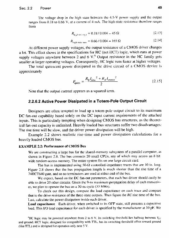
The response of any system of conductors to an incoming signal depends greatly on whether the system is smaller than the effective length of the fastest electrical feature in the signal, or vice versa.
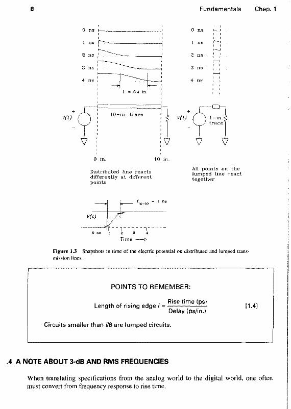
The effective length of an electrical feature, like a rising edge, depends on the time duration of the feature and its propagation delay. For example, let's analyze the rising edge of a IOKH EeL signal. These gates have a rise time of approximately 1.0 ns. This rising edge, when propagating along an inner trace of an FR-4 printed circuit board, has a length of 5.6 in.:
1= ~ D
where I = length of rising edge, in. T,. = rise time, ps D = delay, ps/in.
[1.3]
Figure 1.3 depicts a series of snapshots of the electric potential along a straight trace 10 in. long. A rising edge of I-ns duration impinges on the left end of the trace. Evidently, as the pulse propagates along the trace, the potential is not uniform at all points. The reaction of this system to the incoming pulse is distributed along the trace, which we label a distributed system. The snapshot taken at 4 ns shows the physical length of this rising edge is 5.4 in.
Systems physically small enough for all points to react together with a uniform potential are called lumped systems. Figure 1.3 illustrates the response of a I-in. trace, carrying the same l-ns rising edge, which behaves as a lumped system. The voltage on every part of this line is (almost) uniform at all times.
The classification of a system as distributed or lumped depends on the rise time of the signals flowing through it. The distinguishing characteristic is the ratio of system size to rise-time size. For printed circuit board traces, point-to-point wiring, and bus structures if the wiring is shorter than one-sixth of the effective length of the rising edges, the circuit behaves mostly in a lumped fashion. 3
'Some authors use 1/ .J2rr; others use 1/4. The idea is that small structures are lumped circuits. while big ones are distributed.
8
+ V(t)
0
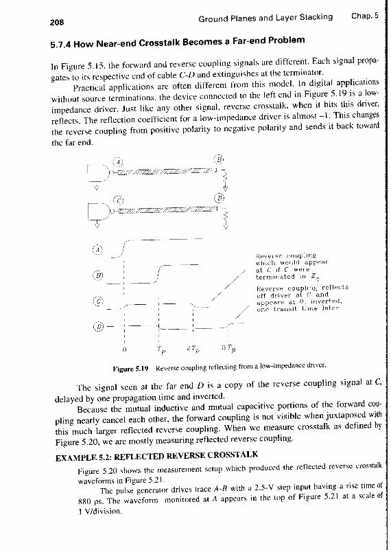
2
3
4
ns I
ns !---ns i ns
~' I I ns I . . . . . .. -----4
I ,
; l = 54 in. ;
10-in. trace
o in. 10 in.
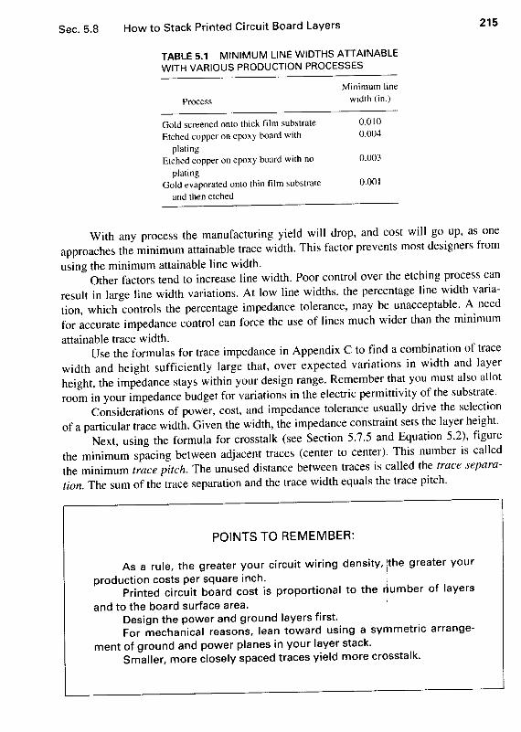
Distributed line reacts differently at different points J r- ',~" ~ , ., V(tJV,~l _ _ T ___ _
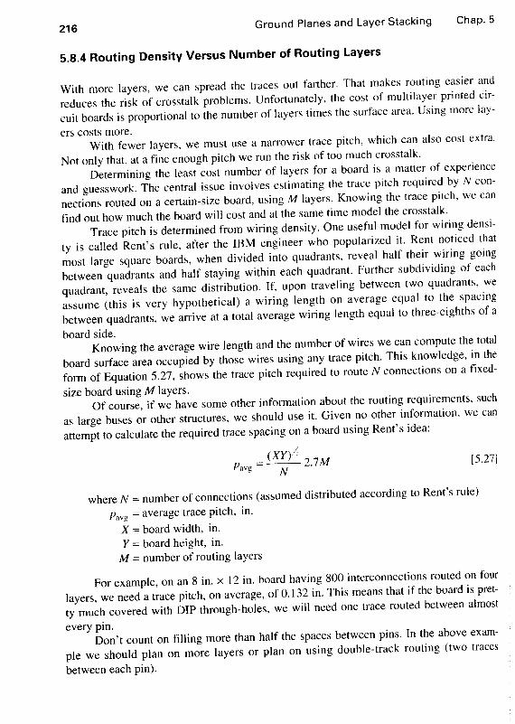
o ns 1 2 3 ..
Time
Fundamentals
I I
0 ns '---J I , I ,
ns r---. I , '-J
2 ns , I , I .---.
3 ns , I
I , <----I
4 ns I
I I , ,
V(t)+~ J tr."~ All points on the lumped line react together
Figure 1.3 Snapshots in time of the electric potential on distributed and lumped transmission lines.
POINTS TO REMEMBER:
Chap. 1
. . Rise time (ps) Length of rlsmg edge I = ------~
Delay (ps/in.) [1.4]
Circuits smaller than //6 are lumped circuits .
. 4 A NOTE ABOUT 3-dB AND RMS FREQUENCIES
When translating specifications from the analog world to the digital world, one often must convert from frequency response to rise time.

Sec. 1.4 A Note About 3-dB and RMS Frequencies 9
For example, oscilloscope manufacturers quote a maximum operating bandwidth for each vertical amplifier and a corresponding maximum bandwidth for each probe. Depending on the manufacturer, they may quote a 3-dB bandwidth or an RMS (noise equivalent) bandwidth. In either case, the conversions between bandwidth and rise time will depend on the exact shape of the scope's frequency response curve.
Fortunately, we do not often need to compute an exact rise time. For the purposes of this book, we may devise an approximate relation that is easy to apply while ignoring complicated details of the exact frequency response shape. Appendix B provides justification for this approach, comparing exact calculations for several different pulse types.
The conversions listed below assume we are translating from frequency response to a 10-90% rise time. As explained in Appendix B, for the accuracy we require in diagnosing and fixing digital problems it hardly matters whether we define rise time using the 10-90% rise time, inverse of the slope at the center of the pulse, or standard deviation method.
where F3dB frequency at which impulse response rolls off by 3 dB r; = pulse rise time (l 0-90%) K :::: constant of proportionality depending on exact pulse shape;
K = 0.338 for gaussian pulses; K = 0.350 for single-pole exponential decay
[ 1.5)
[ 1.6)
If we change our pulse type from gaussian to a single-pole exponential decay, the constant in Equation 1.6 changes from 0.338 to 0.350. For most digital designs, such a subtle distinction hardly matters.
Where a manufacturer quotes the RMS bandwidth, or equivalent noise bandwidth,4 of a subsystem, the following relation computes the 10-90% rise time of that subsystem. Here the constant K changes from 0.36 to 0.55 depending on the pulse type, a slightly more significant change than in Equation 1.6.
T. z K r r
RMS
where FRMS = RMS bandwidth T,. = rise time (10-90%) K == constant of proportionality depending on exact pulse shape;
K 0.361 for gaussian pulses; K = 0.549 for single-pole exponential decay
[ 1.7)
"The noise bandwidth of a frequency response Hi/), or RMS bandwidth, is [he cutoff frequency at which a box-shaped frequency response would pass the same amount of white noise enerty as H(f).

10 Fundamentals Chap. 1
When you look at a scope response to a very fast rising edge (much faster than the scope response), you can usually tell if it has a single-pole or a gaussian-type response. If the leading edge of the response has a sharp comer, suddenly taking off at a steep angle and blending into a long, sweeping tail, it is probably a single-pole response. If the pulse edge sweeps up gently, with symmetric leading and trailing edges, it is probably nearly gaussian. In between, use K = 0.45.
1.5 FOUR KINDS OF REACTANCE
Four circuit concepts separate the study of high-frequency digital circuits from that of low-speed digital circuits: capacitance, inductance, mutual capacitance, and mutual inductance. These four concepts provide a rich language for describing and understanding the behavior of digital circuit elements at high speeds.
There are many ways to study capacitance and inductance. A microwave engineer studies them using Maxwell's equations. A designer of control systems uses Laplace transforms. An advocate of Spice simulations uses linear difference equations. Digital engineers use the step response.
The step response measurement shows us just what we need to see: what happens when a pulse hits a circuit element. From the step response, if we wish, we can derive a curve of impedance versus frequency for a circuit element. In that sense the step response measurement is (at least) as powerful as any frequency-domain measure of impedance.
Our investigation of capacitance and inductance will focus on the step response of circuit elements.
Figure 1.4 illustrates a classic step response measurement for a two-terminal device. In this figure, we use a step source having an output impedance of Rs ohms. The step source is shunted by the device under test, across which we measure the voltage response. In practical measurements, the step input is repeated over and over again while the results are synchronously displayed on an oscilloscope.
X(t) Step
source
Output impedance of step source
/ Device under test shunts the step source
y{t)
Step response
Figure 1.4 Step response test for a two-terminal device.

Sec. 1.6 Ordinary Capacitance 11
With practice, anyone can learn to instantly characterize the device under test by observing the step response and using these three rules of thumb:
(I) Resistors display a flat step response. At time zero, the output rises to a fixed value and holds steady.
(2) Capacitors display a rising step response. At time zero, the step response starts at zero but then later rises to a full-valued output.
(3) Inductors display a sinking step response. At time zero, the output rises instantly to full value and then later decays back toward zero.
To first order, we may characterize any circuit element according to whether, as a function of time, its step response stays constant, rises, or falls. We label these elements resistive, capacitive, and inductive, respectively.
Reactive effects (both capacitance and inductance) further subdivide into ordinary and mutual categories. The ordinary varieties of capacitance and inductance describe the behavior of individual circuit elements (two-terminal devices). The mutual capacitive and inductive concepts describe how one circuit element affects another. In digital electronics, mutual capacitance or inductance usually creates unwanted crosstalk, which we strive to minimize. Plain capacitance or inductance can be a help or a hindrance, depending on the circuit application.
We will define and use a special version of step response for characterizing mutual capacitive and mutual inductive circuit elements.
Our brief study of reactive concepts considers only lumped circuit elements, in this order:
• Ordinary capacitance
• Ordinary inductance
• Mutual capacitance
• Mutual inductance.
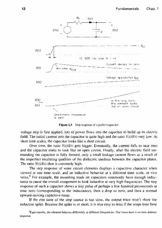
1.6 ORDINARY CAPACITANCE
Capacitance arises wherever there are two conducting bodies charged to different electric potentials. Two bodies at different electric potentials always have an electric field between them. The energy stored in their electric field is supplied by the driving circuit. Because the driving circuit is a limited source of power, the voltage between any two bodies takes a finite amount of time to build up to a steady-state value. The reluctance of voltage to build up quickly in response to injected power, or to decay quickly, is called capacitance. Structures enclosing a large amount of electric flux at low voltages, like two parallel plates, have lots of capacitance.
Figure 1.5 shows idealized current and voltage waveforms for a capacitor driven by a 30-.0 source.5 The step response of a capacitor grows as a function of time. When a
5The 30-0. source is an approximation to the drive capability of a standard TTL output.
12
x(t)
I(t)
y(t)
y(t)
I(t)
Fundamentals Chap. 1
+
X{t) y{t)
10-90% rise time is 1 ns
Current decays to zero
VOltoge approaches Vee
like an open circuit
Short-term impedance is zero
Figure 1.5 Step response of a perfect capacitor.
voltage step is first applied, lots of power flows into the capacitor to build up its electric field. The initial current into the capacitor is quite high and the ratio Y(t)//(t) very low. At short time scales, the capacitor looks like a short circuit.
Over time, the ratio Y(t)/I(t) gets bigger. Eventually, the current falls to near zero and the capacitor starts to look like an open circuit. Finally, after the electric field surrounding the capacitor is fully formed, only a small leakage current flows as a result of the imperfect insulating qualities of the dielectric medium between the capacitor plates. The ratio Y(t)/I(t) then is extremely high.
The step response of some circuit elements displays a capacitive character when viewed at one time scale, and an inductive behavior at a different time scale, or vice versa.6 For example, the mounting leads on capacitors commonly have enough inductance to cause the overall component to look inductive at very high frequencies. The step response of such a capacitor shows a tiny pulse of perhaps a few hundred picoseconds at time zero (corresponding to the inductance), then a drop to zero, and then a normal upward-moving capacitive ramp.
If the rise time of the step source is too slow, the output trace won't show the inductive spike. Because the spike is so short, it is also easy to miss if the scope time base
"Equivalently, the element behaves differently at different frequencies. Our focus here is on time domain response.

Sec. 1.6 Ordinary Capacitance 13
is set for too slow a sweep. It is interesting to contemplate the idea that by adjusting the rise time and setting the time base sweep, we can cause the step response measurement to emphasize the character of a circuit element in a particular frequency range. Roughly speaking, if the step rise time is T" the step response near time zero is related to the impedance magnitude of the circuit element near frequency FA:
r;' _ 0.5 1'A -
T,.
where T,. rise time of step source FA = approximate analysis frequency
[ 1.8]
By visually averaging the step response over a time interval. we can estimate the impedance magnitude at lower frequencies. Use Equation 1.8 to compute the approximate analysis frequency that corresponds to an averaging interval of T, ..
The final value of the step response indicates the impedance magnitude at DC. With a step rise time of T,.. we cannot infer much about the behavior of the compo
nent at frequencies greater than FA- Make sure your step source is fast enough to reveal what you want to see.
Figure 1.6 shows a measurement setup ideal for characterizing capacitors of a few picofarads over a time interval of nanoseconds, This arrangement is ideal for characterizing the capacitance of circuit traces, gate inputs, bypass capacitors, and other common digital circuit elements. This method drives the capacitor under test with a known resis-
r------., ...... ] Internal 50 n , back termination
Pulse I generator~
50 (I
Internal 50.0 termination
V(t) ~\
~''' .. ___ .... _ ....... ____ l _____ i __ n ______________ _ ; _.. . square ;
( . \ ~.~
All resistors 1/8 W
Run coax probes in from opposite sides to reduce direct feed-through
Ground out DUT test point to check for feed~through
Device under test (DUT) goes between these terminals
Figure 1.6 A 500-11 lab setup for measuring capacitanceL

14 Fundamentals Chap. 1
tance. By measuring the rise time of the resulting waveform, we can infer a value for the capacitance. In comparison to techniques used at audio frequencies, this setup is very complicated. The complication follows from the difficulty of containing and directing electromagnetic field energy at high frequencies. The coaxial cables are used to direct the test signals and measured results into and out of a solid ground plane area no more than I in.2 where the actual measurement takes place. Limiting the measurement footprint to I in.2 ensures that the circuit will behave in a lumped fashion.
Example 1.1: Measurement of a Small Capacitance to Ground
The device under test (DUT) in this example (Figure 1.6) is a parallel plate capacitor, 0.5 in. x 0.75 in., printed in 1+ -oz copper on an epoxy FR-4 printed circuit board, nominally 0.008 in. above a solid ground plane. This structure forms a capacitor with extremely low parasitic series inductance.
The measurement setup consists of two RG-174 coaxial eables, IN and OUT. The IN cable, terminated with 50 a to ground, includes a I K drive resistor connected from the terminated output to the device under test. The IK resistor isolates the signal source from the device under test, providing to the source a constant terminating impedance regardless of the impedance of the OUT. Isolation ensures consistent source rise time and amplitude performance regardless of the OUT load impedance.
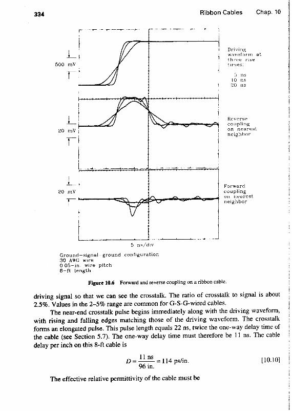
The source pulse generator provides signals of similar amplitude and rise time as that expected in the actual circuit. When measuring passive components, the DC offset of the pulse generator does not much matter. On the other hand, when measuring gate inputs, always adjust the pulse source to span the input switching range and apply power to the gate under test. That biases the gate into its operating range for the test. Gates requiring lots of input drive current may need source resistors smaller than I Kn.
If your signal generator has a 50-a back-termination feature, engage it to reduce reflections on the IN cable. This feature inserts 50 a in series with the signal generator output, reducing ret1ections back and forth along the source cable between the unavoidable slight mismatch at the test jig and the output impedance of the signal source. Using the back termination, unwanted reflections from your source signal now are attenuated first when they bounce off the test jig and a second time as they bounce off the back termination resistor in the signal source on their return path to your measuring apparatus. The back termination reduces the available source drive amplitude by half but improves the system step response.
The OUT cable connects separately through I K a to the circuit under test, running to an oscilloscope input internally terminated with 50 a. The I K resistor acts as a 21: I probe. The advantages of this sensing arrangement are detailed later in this book in the section on oscilloscope probing. Both IN and OUT cables are 3 ft long.
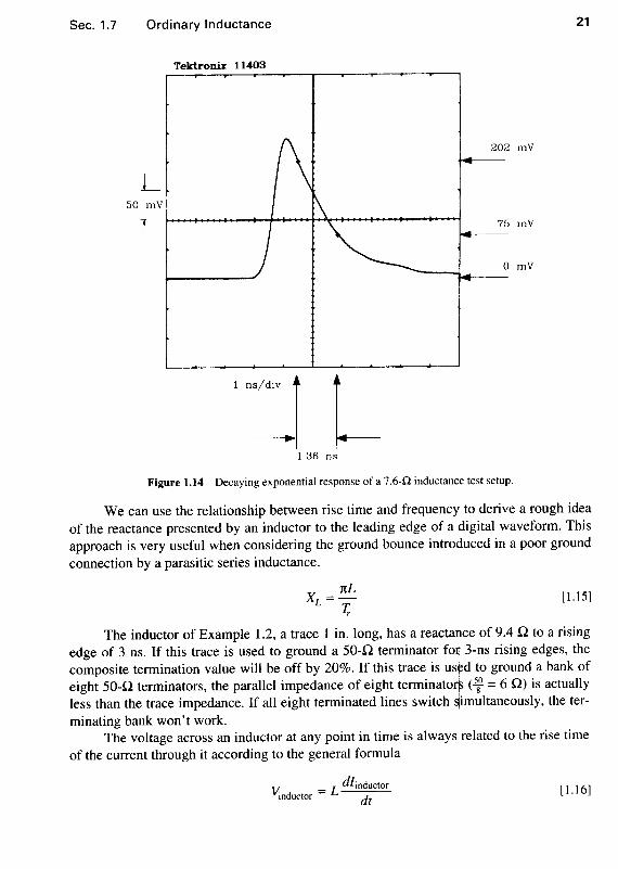
The open-circuit response of this probe, when driven by a 2.6-Y step input from the source with the OUT disconnected, appears in Figure 1.7. The top trace is recorded at 5 ns/division, and the bottom trace is an exploded view of the same signal at 500 ps/division.
The Tektronix 11403 scope used to record this waveform automatically computes a 10-90% rise time of 818 ps. The nominal step amplitude is 63 mY (the scope measures a
7Longer cables can be an advantage. in that reflections occur so late that they do not show on the scope. The disadvantage to longer cables is that they introduce more signal dispersion. At some length the cable response begins to deteriorate the observable rise time. [n Figure 1.7 retlection effects from the 3-ft cables show up about 8 ns into the picture.

Sec. 1.6 Ordinary Capacitance 15
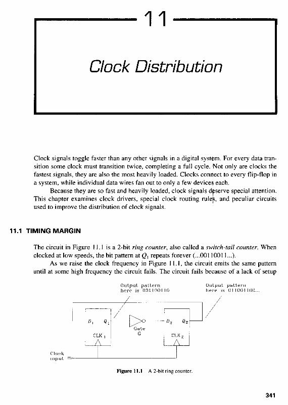
Tektronix 11403 , , --
L """" f
10 mV
r
'--............... 5 ns/div
~--------------------- -----=-::=--------1 L r==-------------
500 ps/div
Figure 1.7 Open-circuit response of a 500-Q capacitance test setup.
peak of 67 mY). Note that the measured step amplitude is t the amplitude at the DUT of 1.3 V, which is in tum half the source drive voltage.
The Thevinen equivalent circuit for this test arrangement, as shown in Figure 1.8, includes the aggregate system rise time lumped into the source. It matters not whether the signal source or the scope contributes more to the slowness of the observed rise time. Any reasonable combination of source and scope having a similar open-circuit rise time will behave similarly under the influence of the DUT. It matters only that we know the aggregate rise time of the source scope combination. When measuring passive components, it similarly matters only that we know the observed step amplitude, details of the actual voltage at the DUT and the probe attenuation ratio being unimportant.
503n
+
x{t)
83-mV step
820-ps 10-90% rise time
y{t)
Figure 1.8 Theve:nin equivalent of a 500-Q capacitance test setup.
16 Fundamentals Chap. 1
The source impedance is 503 fl, as measured at the OUT terminals using an ohmmeter with the pulse source turned off but the back termination to 50 n still connected. This 503 n is the parallel combination of the I K drive resistor and the I K sense resistor.
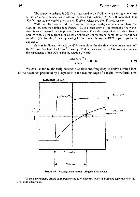
With the DUT connected, the observed voltage displays a capacitive character, starting low and then rising (see Figure 1.9). A stored copy of the original drive waveform is superimposed on this picture for reference. Over the range of time scales observable with this probe, from 800 ps (the aggregate source-probe combination rise time) to 40 ns (the length of trace appearing in the scope photo) the DUT appears perfectly capacitive.
Cursors in Figure 1.9 mark the 63% point along the rise time where we can read off the RC time constant of 23.5 ns. 8 Knowing the drive resistance of 503 n, we can compute the capacitance of the DUT using the relation C::::: 'tIR:
C 23.5 x JO-ll9 S
503 n 46.7 pF [1.9]
We can use the relationship between rise time and frequency to derive a rough idea of the reactance presented by a capacitor to the leading edge of a digital wavefonn. This
TektroDb: 11403
63.0 mV .. L
10 mY 39.7 mY ..
0.6 mY
LnS/divJ 23.5 ns
Figure 1.9 Finding a time constant using the 63% method.
gIn one lime constant, a rising edge progresses to 63% of its final value, and a falling edge deteriorates to 37% of its initial value.

Sec. 1.7 Ordinary Inductance 17
approach is very useful when considering the distortion introduced in a digital waveform by a capacitive load.
'Ty Xc =
n:C [1.1 0)
The capacitor in Example 1.1 has a reactance of 20.44 Q to a rising edge of 3 ns. We therefore predict it will significantly distort (by slowing down) a 3-ns rising edge from a TTL driver having an output impedance of 30 Q.
The current through a capacitor at any point in time is always related to the rise time of the voltage across it according to the general formula
d\{apacitor [capacitor = C dt [1.11]
Equation 1.11 will help us later when calculating crosstalk due to capacitance between circuits.
POINT TO REMEMBER:
A capacitance test jig is easy to build using a pulse source and an oscilloscope.
1.7 ORDINARY INDUCTANCE
Inductance arises wherever there is electric current. Electric current creates a magnetic field, with the energy stored in the magnetic field supplied by some driving circuit. Because any driving circuit is a limited source of power, current always takes a finite amount of time to build up to a steady-state value. The reluctance of current to build up quickly, or to decay quickly, is called inductance.
Figure 1.10 shows idealized current and voltage waveforms for an inductor driven by a 30-Q source. The step response of an inductor shrinks as a function of time. When a voltage step is first applied, almost no current flows, making the ratio y(t)II(t) very high. At short time scales, the inductor looks like an open circuit.
Over time, the ratio Y(t)/I(t) decays. Eventually, the voltage drops to near zero and the inductor starts to look like a short circuit. Later, after the magnetic field surrounding the inductor is fully formed, the current is limited only by the DC resistance of the inductor. The ratio Y(t)lI(t) is then extremely low.
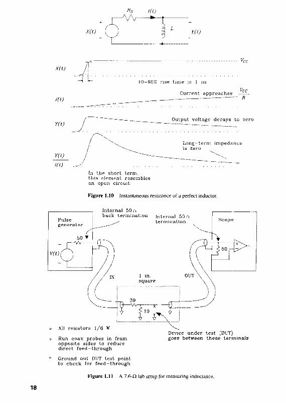
Figure 1.11 shows a measurement setup optimized for characterizing inductors of a few nanohenries. This arrangement is ideal for measuring the inductance of ground traces or short lengths of connecting wiring.
18
X(t)
1ft)
Y(t)
Y(t)
I(t)
Rs I{t)
+
x(t)
In the short term. this element resembles an open circuit
y(t)
Vee
Current R
voltage decays to zero
Long-term impedance is zero
Figure 1.10 Instantaneous resistance of a perfect inductor.
Pulse generator
Internal 50 {l back termination Internal 50 n.
termination
50'" I
)~ LV_(t_) ~====j'/; IN
+
( 1 in. square
Scope
All resistors liB W Device under test (DUT)
Run coax probes in from opposite sides to reduce direct feed-through
Ground out DUT lest point to check for feed-through
goes between these terminals
Ji'igure 1.11 A 7.6-Q lab setup for measuring inductance.

Sec. 1.7 Ordinary Inductance 19
EXAMPLE 1.2: Measurement of a Small Inductance to Ground
The device under test (OUT) in this example (Figure 1.11) is a short I-in. circuit trace printed in 'f -oz copper on an epoxy FR-4 printed circuit board. The trace nominally rides 0.008 in. above a solid ground plane and is 0.0' 0 in. wide. The far end of the trace is shorted to ground with a 0.035-in.- diameter via. This structure has a parasitic capacitance to ground of 2 pF when open-circuited, and half that when the far end is shorted. 9 The calculated inductance is about 9 nH.
We plan to characterize this circuit using an 800-ps rise time. First check that the parasitic capacitive reactance at that speed is much larger than the inductive reactance we wish to see.
[ 1.12]
TtL 35 Q r 1.131
The capacitive reactance, which appears in parallel with our measurement, is eight times bigger than the expected inductive reactance. The effect of this capacitance will be to increase our observed value of LIR by about 12%.
The measurement setup consists of two RG-174 coaxial cables, IN and OUT. The IN cable, terminated in a total of 49 Q to ground, includes a tap of 10 Q for driving the OUT. In this jig the source is not as well isolated from the OUT as in the capacitance test jig. The terminating impedance seen by the source varies from 39 to 49 Q under various OUT load conditions.lO Because we expect reflections off the mismatch at the OUT, do not forget to back-terminate your pulse generator.
The generator is adjusted for no DC offset. The inductor would short out any DC offset anyway.
The source impedance is 7.6 Q as measured at the OUT with the source turned off but the back termination connected. This is a parallel combination of the 50 + 39-Q source impedance, the IO-Q tap resistor, and the 50-Q probe impedance.
We have arranged for a low source impedance at the OUT to exaggerate the LIR decay time. Had we used a test jig with a 500-Q Thevenin equivalent source resistance, the expected LlR time would be only 0.018 ns. With a 7.6-Q source we expect a 1.2-ns LIR decay constant.
The OUT cable connects directly to the OUT in this experiment and runs to an oscilloscope input internally terminated with 50 Q. Both IN and OUT cables are 3 ft long.
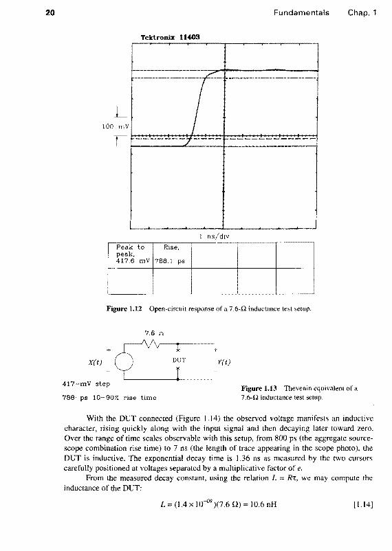
The open-circuit response of this 7.6-Q test setup, when driven by a 2.4-V step input, appears in Figure 1.12. The scope automatically computes a 10-90% rise time of 788 ps. The step amplitude is 417 mY. The probe is a 1:1 arrangement, so the voltage at the OUT is actually 417 mY.
Figure 1.13 shows the Thevenin equivalent circuit of this 7.6-Q test setup.
"For those familiar with short transmission line theory, according to the pi model (C+L+C) for a short transmission line shorting the far end just shorts out one of the two capacitors. The result is a tank circuit composed of the full inductance and half the open circuit capacitance.
'''Because the short-term impedance of the inductor is high, the best choice for the terminating network is 39 and 10 n. giving a 49-0 initial value. This terminates the initial rising step edge with 49 O. Were we measuring the low-inductance capacitor of Example 1.1, the best choice would be 50 and lO ohms. because the short-term impedance of a capacitor is initially zero.
20 Fundamentals Chap. 1
Tektronix 11403
----------------------~t__------_I ,--------------- --- -------------------
L 100 mV
II--__ ~f:_ ______ r ____________ _
I ns/div
Peak to Rise, I
peak, 417.6 mV 768.1 ps
I ,
Figure 1.12 Open-circuit response of a 7.6-Q inductance test setup.
7.6 n
+ +
X(t) Y(t)
417-mV step
788-ps 10-90% rise time Figure 1.13 Thevenin equivalent of a 7.6-Q inductance test setup.
With the DUT connected (Figure 1.14) the observed voltage manifests an inductive character, rising quickly along with the input signal and then decaying later toward zero. Over the range of time scales observable with this setup. from 800 ps (the aggregate sourcescope combination rise time) to 7 ns (the length of trace appearing in the scope photo), the OUT is inductive. The exponential decay time is 1.36 ns as measured by the two cursors carefully positioned at voltages separated by a multiplicative factor of e.
From the measured decay constant, using the relation L := Ri:, we may compute the inductance of the OUT:
L:= (1.4 x 10-09)(7.6 Q):= 10.6 nH [1.14)