high speed backbone for fpga at ess -...
TRANSCRIPT
Hig
h Sp
eed B
ackbo
ne fo
r FPGA
at ESS
Department of Electrical and Information Technology, Faculty of Engineering, LTH, Lund University, 2016.
High Speed Backbone forFPGA at ESS
Max AnderssonGabriel Jönsson
Series of Master’s thesesDepartment of Electrical and Information Technology
LU/LTH-EIT 2016-482
http://www.eit.lth.se
Ma
x An
de
rsson
& G
abriel Jö
nsso
n
Master’s Thesis
High speed backbone for FPGA at ESS
Gabriel Jö[email protected]
Department of Electrical and Information TechnologyLund University
Advisor: Fredrik Kristensen
January 20, 2016

Printed in SwedenE-huset, Lund, 2016

Abstract
The purpose of this project is to reverse engineer and re-design a PCI Expresscommunication system which is currently being used at ESS in Lund. The currentmodel is non-modifiable and our goal is to create a system open for customization.The aspects explored are communication between hardware and software usingPCI Express, data handling and arbitration, direct memory access and how thesecan be implemented in hardware. We have successfully re-created the originaldesign with a fully utilized read interface and a significantly slower write interface.The write function has been studied to find possible options to improve the currentdesign. This system will be installed in 150 different parts of the accelerator andalthough it is a small part, it will be vital for the overall performance.
i

ii

Acknowledgments
A lot of thanks to the warmth and guidance received from the people around us.Fredrik Kristensen you have committed a lot of time and effort to assist and inspireus during the last five months. Yeimy Lopez and Jessica Ericsson you have givenus hope and comfort when everything seemed hopeless. For this we thank youand all of the competent people at ESS that helped us in any way. Urša Rojec,Klemen Strnisa, Maurizio Donna and Niklas Claesson; thank you too for yourcontributions. We would also like to thank Fredik Rusek for taking the role asexaminer.
iii

iv
Table of Contents
1 Introduction 11.1 Background . . . . . . . . . . . . . . . . . . . . . . . . . . . . . . . 11.2 Purpose of the project . . . . . . . . . . . . . . . . . . . . . . . . . 2
1.2.1 Practical application 21.2.2 Goals 3
1.3 Thesis structure . . . . . . . . . . . . . . . . . . . . . . . . . . . . . 6
2 Theory 92.1 PCI Express . . . . . . . . . . . . . . . . . . . . . . . . . . . . . . . 9
2.1.1 Compability 92.1.2 Root complex structure 92.1.3 Enumeration 102.1.4 PCIe hierarchy 112.1.5 TLP - Transaction layer package 12
2.2 AXI - Advanced eXtensible Interface . . . . . . . . . . . . . . . . . . 152.2.1 Master/Slave 16
3 System 173.1 Development tools . . . . . . . . . . . . . . . . . . . . . . . . . . . 17
3.1.1 ISE project navigator 173.1.2 iMPACT 17
3.2 Debugging tools . . . . . . . . . . . . . . . . . . . . . . . . . . . . 173.2.1 ISim - ISE simulator 173.2.2 Questasim 183.2.3 Analyzer 18
3.3 Hardware equipment . . . . . . . . . . . . . . . . . . . . . . . . . . 18
4 Implementation 194.1 Architecture overview . . . . . . . . . . . . . . . . . . . . . . . . . . 194.2 PCI Express interface . . . . . . . . . . . . . . . . . . . . . . . . . . 19
4.2.1 Ingress 194.2.2 Egress 224.2.3 Register file 23
v

4.2.4 DMA 274.3 AXI interconnect - read/write arbiter . . . . . . . . . . . . . . . . . 284.4 Memory interface . . . . . . . . . . . . . . . . . . . . . . . . . . . . 29
4.4.1 AXI controller 304.4.2 User interface 304.4.3 Memory interface controller 30
5 Verification 335.1 Test bench . . . . . . . . . . . . . . . . . . . . . . . . . . . . . . . 335.2 Chipscope . . . . . . . . . . . . . . . . . . . . . . . . . . . . . . . . 335.3 Software tests . . . . . . . . . . . . . . . . . . . . . . . . . . . . . . 33
6 Results 356.1 Design resources . . . . . . . . . . . . . . . . . . . . . . . . . . . . 356.2 Performance . . . . . . . . . . . . . . . . . . . . . . . . . . . . . . 36
6.2.1 Clock frequency 366.2.2 Read 366.2.3 Write 36
7 Analysis 377.1 Conclusions . . . . . . . . . . . . . . . . . . . . . . . . . . . . . . . 377.2 Lessons Learned . . . . . . . . . . . . . . . . . . . . . . . . . . . . 387.3 If we were to do it again . . . . . . . . . . . . . . . . . . . . . . . . 407.4 Future work . . . . . . . . . . . . . . . . . . . . . . . . . . . . . . . 40
References 43
vi

List of Figures
1.1 Overview of the LLRF system setup. . . . . . . . . . . . . . . . . . . 21.2 Setup for cavity testing and electric field regulation . . . . . . . . . . 31.3 First set goal of the project. . . . . . . . . . . . . . . . . . . . . . . 41.4 Second set goal of the project. . . . . . . . . . . . . . . . . . . . . . 41.5 Third set goal of the project. . . . . . . . . . . . . . . . . . . . . . . 51.6 Fourth set goal of the project. . . . . . . . . . . . . . . . . . . . . . 51.7 Fifth set goal of the project. . . . . . . . . . . . . . . . . . . . . . . 6
2.1 Example of a PCIe system with a root complex and multiple endpointsin the form of one memory, two PCIe endpoints and a PCI/PCI-X buswhich can be connected with multiple peripherals which are compatiblewith older bus standards. . . . . . . . . . . . . . . . . . . . . . . . . 10
2.2 Simple representation of a link between the layers of two PCIe devices. 112.3 The contents of a TLP. The parts added by the individual layers are
marked with dotted lines. The Data and ECRC data blocks are op-tional dependent on the purpose of the package. . . . . . . . . . . . 12
2.4 The first header present in all TLPs [5] . . . . . . . . . . . . . . . . 132.5 The TLP header with the additional memory request header. . . . . 142.6 The TLP header with the additional completion header. . . . . . . . 142.7 AXI communication between master and slave. . . . . . . . . . . . . 15
3.1 SIS8300-L MTCA.4 Digitizer Struck Board . . . . . . . . . . . . . . 18
4.1 Overview of the system as a whole. . . . . . . . . . . . . . . . . . . 204.2 FSM with transaction triggers in block Ingress . . . . . . . . . . . . 214.3 FSM with transaction triggers in block Egress . . . . . . . . . . . . . 224.4 FSM with transaction triggers in block DMA . . . . . . . . . . . . . 284.5 Structure of the interconnect. . . . . . . . . . . . . . . . . . . . . . 294.6 Simple representation of the interconnect arbiter. . . . . . . . . . . . 294.7 Overview of the memory interface. . . . . . . . . . . . . . . . . . . . 304.8 Memory initialization process performed by the physical layer in the
memory interface. . . . . . . . . . . . . . . . . . . . . . . . . . . . . 31
7.1 Illustration of correct/incorrect RTL code hierarchy. . . . . . . . . . 39
vii

viii

List of Tables
2.1 TLP formats . . . . . . . . . . . . . . . . . . . . . . . . . . . . . . 132.2 TLP types . . . . . . . . . . . . . . . . . . . . . . . . . . . . . . . . 13
4.1 Register address mapping . . . . . . . . . . . . . . . . . . . . . . . 244.2 Register 0x021 - Memory steady state signals . . . . . . . . . . . . . 254.3 Register 0x221 - IRQ status . . . . . . . . . . . . . . . . . . . . . . 274.4 Register 0x222 - IRQ clear . . . . . . . . . . . . . . . . . . . . . . . 274.5 Memory specification parameters needed for the memory interface. . 30
6.1 Device utilization extracted from place and route report. . . . . . . . 356.2 Logic distribution extracted from place and route report. . . . . . . . 356.3 Part of specific feature utilization from place and route report. . . . . 36
7.1 SDRAM command control signals . . . . . . . . . . . . . . . . . . . 40
ix

x

Abbreviations
ESS European Spallation Source
FPGA Field-Programmable Gate Array
AXI Advanced eXtensible Interface
PCIe Peripheral Component Interconnect Express
I/O Input/Output
ADC Analog to Digital Converter
DAC Digital to Analog Converter
CPU Central Processing Unit
TLP Transaction Layer Package
BDF Bus, Device, Function
BAR Base Address Register
MIG Memory Interface Generator
DDR3 Double Data Rate type Three
SDRAM Synchronous Dynamic Random Access Memory
RTL Register-Transfer Language
IP Intellectual Property
FIFO First In First Out
LLRF Low Level Radio Frequency
DMA Direct Memory Access
FSM Finite State Machine
xi

Chapter1Introduction
This chapter summarizes the report and explains both the motivation and thereason for this project being created. We introduce a background of how the ESSparticle accelerator will be used to split atoms to create neutrons, and we alsohighlight the goals and purposes of this work to give the reader a good overviewof this project.
1.1 BackgroundThe European Spallation Source (ESS) is a multi-disciplinary research facilitybased on what will be the world’s most powerful neutron source [1]. It is a largecollaboration between 17 different countries with employees from over 40 differentnations. The facility will be built in Lund and is projected to reach full capacityin 2025 with a run time of 5000 hours a year and reliability of 95% [2].
ESS will technically include four building parts:
1. The first part is the ion source responsible for delivering a proton beam.For the facility’s current specifications the planned component for this partis a compact Electron Cyclotron Resonance (ECR) source. The beam isplanned to fire with a frequency of 14 Hz and should be held for a periodof 2.86 ms. The reliability should reach 99.9% and thereby only contribute0.1% to the total uncertainty.
2. Within the next part, the accelerator, the protons from the ion source arepushed together and accelerated through the facility. 150 cavities are placedalong the 600 meter long tunnel to accelerate and guide the beam. Eachof these cavities will be connected with a Field-Programmable Gate Array(FPGA), which will be responsible for real time regulation of the electricfield inside the cavity. An overview of the regulator system is shown inFigure 1.1. The idea is to regulate the field so that the proton beam hits iton it’s positive flank, making the protons accelerate. This is in theory doneby representing sampled data on the IQ plane and multiplying them with arotation factor to get to the sought positions [3].The FPGA is also connected to a Central Processing Unit (CPU) responsiblefor the FPGA setup, longtime logging and multi-pulse algorithms.
1

2 Introduction
Figure 1.1: Overview of the LLRF system setup.
3. The purpose of the target is to transform high powered proton beams to lowenergy neutron beams. This is achieved by spallation, a process in whichsplitter is ejected from a body after it is hit by a large impact. In thiscase the impact will be produced by the accelerated proton beam. In thisproject the body (the target) is specified as a rotating wheel of tungstencooled by helium gas. An important factor of this target is a radiationshielding system consisting of approximately 7000 tons of steel. This iscrucial since spallation not only emits neutrons but also dangerous gamma-and fast neutron radiation.
4. Research instruments constitute the final part of ESS. The facility is plannedto have 22 research instruments running in 2025. These instruments gatherneutrons to support research in a multitude of fields such as medicine,biotechnology and energy.
1.2 Purpose of the project1.2.1 Practical applicationThis application is meant to serve as an intermediary between software (SW)driven applications and the FPGA. Figure 1.2 shows the setup for cavity testingas it is today, where our design is placed on the digitizer board in the MTCA.4crate to help the Low-Level Radio Frequency (LLRF) control system communicatewith the CPU. As of today there is a working design for the communication partbut its functionality is questionable. The original design was bought from a third

Introduction 3
party company that only provided a netlist file with constraint information (NGC)for implementation. This makes it impossible to change or adapt the functionality.To get full control of the implementation it would have to be rebuilt in-house. Sincethis design has to fit with the current design SW, all settings and parameters ofthe black-boxed design will therefore have to be reverse engineered.
Figure 1.2: Setup for cavity testing and electric field regulation
1.2.2 Goals
At the start of the project a number of partial goals were decided on, both theo-retical and practical. The theoretical parts encompass the general understandingof how a modern particle accelerator works. The practical parts will be designedin both firmware and software and will be divided into five smaller milestones.By proceeding in this manner the project will have a better structure and theaccomplishments will be easier to measure.
Goal 1
The first goal will be to create the custom Peripheral Component InterconnectExpress (PCIe) interface, as shown in Figure 1.3. The goal will be fulfilled whencommunication between software and the interface behaves as the built in version.
4 Introduction
Figure 1.3: First set goal of the project.
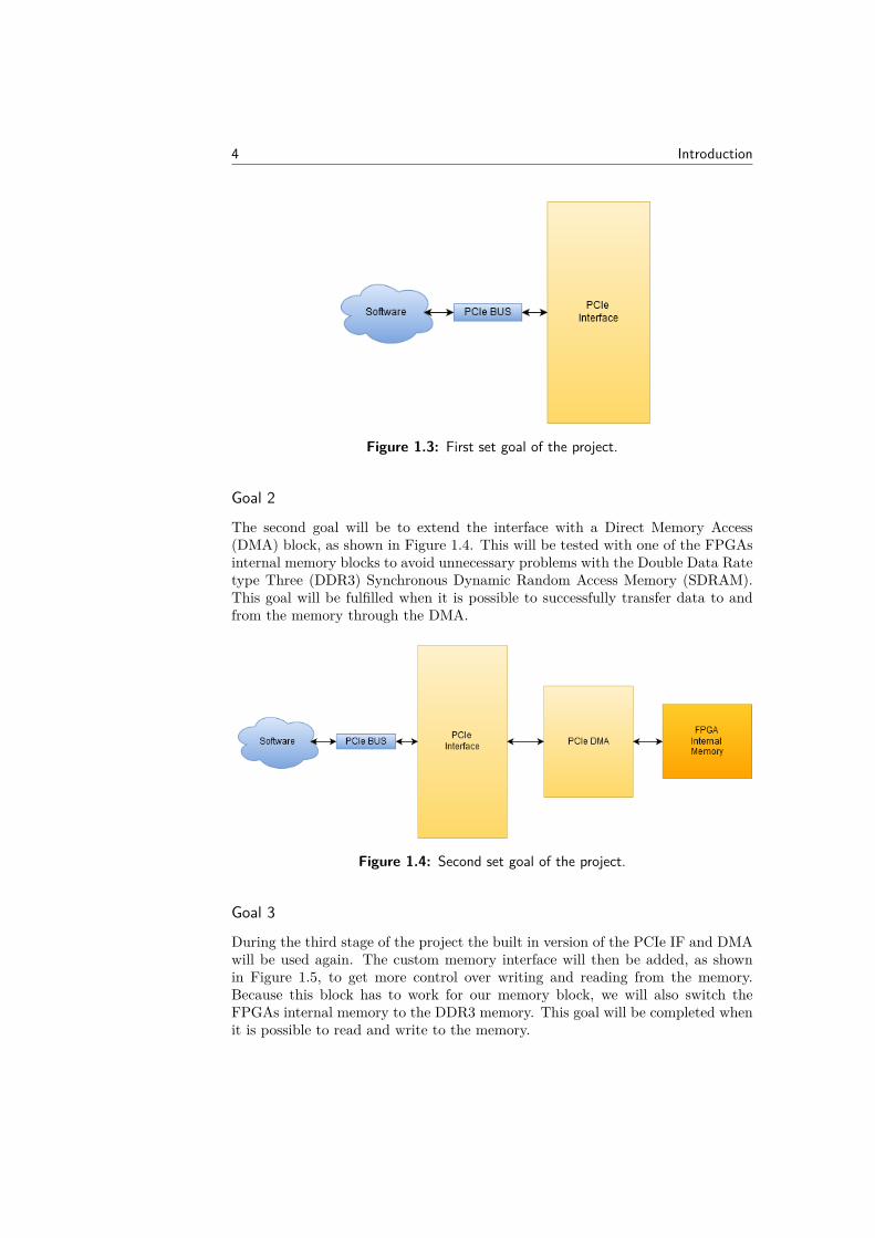
Goal 2
The second goal will be to extend the interface with a Direct Memory Access(DMA) block, as shown in Figure 1.4. This will be tested with one of the FPGAsinternal memory blocks to avoid unnecessary problems with the Double Data Ratetype Three (DDR3) Synchronous Dynamic Random Access Memory (SDRAM).This goal will be fulfilled when it is possible to successfully transfer data to andfrom the memory through the DMA.
Figure 1.4: Second set goal of the project.
Goal 3
During the third stage of the project the built in version of the PCIe IF and DMAwill be used again. The custom memory interface will then be added, as shownin Figure 1.5, to get more control over writing and reading from the memory.Because this block has to work for our memory block, we will also switch theFPGAs internal memory to the DDR3 memory. This goal will be completed whenit is possible to read and write to the memory.

Introduction 5
Figure 1.5: Third set goal of the project.
Goal 4
Here the custom blocks from goal two and three are combined, as shown in Figure1.6. No new blocks are added. This goal will be completed when goal two andthree are completed again in the combined system.
Figure 1.6: Fourth set goal of the project.
Goal 5
By adding the analog to digital input from the cavities, as shown in Figure 2.7,a new interface is added to the system. Now there are two different inputs thatcan write to memory. Since the software and the data from the cavities can notwrite to memory at the same time, a write arbiter is needed. The purpose of thisarbiter is to control which input gets access to the memory and which input getsdelayed. This goal will be completed when the arbiter can give correct priority totwo different inputs and write the correct input to memory.

6 Introduction
Figure 1.7: Fifth set goal of the project.
Optional final goalTime permitting, a final goal could be defined through the addition of a readarbiter.A read arbiter has the same purpose as the write arbiter from the fifthgoal, the difference being that it manages reading from memory instead of writing.
1.3 Thesis structureHere follows a short description of the chapters introduced in this report.
IntroductionIntroduces the project and motivation to the thesis.
TheoryExplains some of the concepts used during the thesis.
SystemIntroduces the tools and equipment used during our work.
ImplementationExplains the functionality of all the included blocks.
VerificationDescribes the tools used during verification.
ResultsPresents the final results of the finished project.

Introduction 7
AnalysisDiscusses our experience of this project and possible future work which couldadvance the system.
ReferencesLists the references that have been used during the thesis.

8 Introduction

Chapter2Theory
This chapter introduces multiple concepts such as the different bus systems thathave been used throughout the project. Only the most general and relevant partsare included and described thoroughly.
2.1 PCI Express2.1.1 CompabilityPCIe is a third generation input/output (I/O) bus standard with second generationpredecessors PCI and PCI-X. The new bus is backwards compatible with the oldstandards though, and can therefore be used together with older systems. Thisfeature simplifies the plug and play functionality of the bus as long as the connectedperipherals are compatible with the older bus standards.
One of the large differences of this version compared with the older standards isthe difference in internal connectivity of the bus. Both PCI and PCI-X use a multi-drop parallel interconnected shared bus model. This means that the system hasone bus that all peripherals are connected to and through which they communicatewith each other in parallel. PCIe devices do not work simultaneously in parallel butin serial point-to-point connections. Instead of communicating with a shared bus,the devices are connected with switches or direct connections to a root complex.PCI and PCI-X buses can be connected to the root complex as if they were PCIeendpoints, making the whole structure backwards compatible.
2.1.2 Root complex structureA root complex is used to connect the CPU and memory subsystems to PCIeconnections. This helps to relieve the CPU from work since the root complexgenerates memory and I/O packages in response to the transactions sent by theCPU. The same transactions can also be received from devices located furtherdownstream in the hierarchy. These devices can either be switches that allowthe root port to connect to more devices than it has available ports, or endpointdevices that are all requesters or completers of PCIe transactions. An example of aroot complex system is shown in Figure 2.1. Memory blocks, Ethernet connectorsor graphic devices can all be endpoints if they follow the PCIe standard.
9

10 Theory
Figure 2.1: Example of a PCIe system with a root complex and mul-tiple endpoints in the form of one memory, two PCIe endpointsand a PCI/PCI-X bus which can be connected with multipleperipherals which are compatible with older bus standards.
2.1.3 Enumeration
Since there is no available information at start up the CPU needs a method to iden-tify the surrounding PCIe devices. Enumeration is a process that makes it possibleto identify the connected devices by finding the corresponding Vendor- and DeviceID numbers. These numbers are found at address zero of the PCIe compatibilityregisters of each PCIe device. During enumeration the CPU addresses all possibledevices by going through all Bus, Device, Function (BDF) numbers. If a deviceexists on the specified port the device will answer with its ID numbers whereas ifno device is present on the specified slot a value of all ones is returned. When alldevices that incorporate a Base Address Register (BAR) and have valid device-and vendor IDs have been enumerated, the CPU can start sending transactions.The addresses stay valid until the system is powered down and the settings arelost. Once the system turns on again, the enumeration process restarts.

Theory 11
Figure 2.2: Simple representation of a link between the layers of twoPCIe devices.
2.1.4 PCIe hierarchyThe communication between PCIe devices is managed by transmission and recep-tion of packages. These packages are called Transaction Layer packages (TLP)since they originate from the Transaction Layer of the PCIe hierarchy. This layeris located at the top of the hierarchy, and is followed by the Data Link Layer andthe Physical Layer.A simplified version of how these layers communicate is shownin Figure 2.2 [4].
Transaction LayerThe Transaction Layer contains buffers that are used to store inbound and outgoingTLPs. The packages sent to the receiver are assembled with the data header, datapayload, and depending on whether it is included in the specification, an end toend Cyclic Redundancy Check (CRC) field. On the receiving side this process isreversed by extracting the information from the package before sending it to the

12 Theory
device core. If the receiver buffer is full at the time a new transmission is startedthen the package is stalled on the transmission side. This is a feature called flowcontrol and is implemented on the hardware level of the PCIe protocol.
Data Link LayerWhen receiving a TLP from the Transaction Layer, the Data Link Layer adds asequence number and a Link CRC field to the header. Before sending the packageon to the Physical Layer, a copy of the TLP is saved in a replay buffer. Whenthe package is received by the Data Link Layer of the other device the CRC fieldis checked for errors. If there is no error an Acknowledge (ACK) package is sentback. When the acknowledgement is received the specified TLP is cleared fromthe replay buffer. On the other hand, if there is an error, a NACK is sent back tothe transmitter. The transmitter then retransmits the TLP from the replay buffer.In this way the transmission is self correcting on a transmission level without theinvolvement of SW.
Physical LayerThe physical layer only has a minor role in affecting the outgoing packages in theform of adding a start/end bit at the respective sides of the package. These bits arecalled framing bits, as shown in Figure 2.3. The receiving side of the connectionuses these bits to determine where the packages start and end. In addition to thistask the physical layer is responsible for link training and initialization. Theseprocesses configure both sides of a link to be synced with each other. An exampleof one such configuration is where a device with two data lanes is connected to adevice with four data lanes. In such case the initialization process decides whichtwo of the four lanes on the second device shall be connected to the two of thefirst device.
Figure 2.3: The contents of a TLP. The parts added by the individuallayers are marked with dotted lines. The Data and ECRC datablocks are optional dependent on the purpose of the package.
2.1.5 TLP - Transaction layer packagePackages leaving the transaction layer can have multiple purposes e.g. memory- orI/O requests. Independent of what kind of package it is, the first four byte headerof the TLP always has the same structure as shown in Figure 2.4. The Reserved

Theory 13
(R) fields in the header must be left as zeros and are unmodified on their way tothe receiver. The other fields are important for knowing what the purpose of thepackage is and what kind of attributes it has.
Figure 2.4: The first header present in all TLPs [5].
The Format (FMT) field indicates how big the header is in Double Words(DW - 32 bits) and if the package contains data or not as shown in Table 2.1. Inthe case of this system, only header sizes of three DWs are used since only 32-bitaddresses are supported.
Table 2.1: TLP formats
FMT TLP format00 3 DW header, no data01 4 DW header, no data10 3 DW header, with data11 4 DW header, with data
Type decides on the purpose of the package. In this system the formats neededare shown in Table 2.2, although in the general case up to 17 different format andtype combinations can be supported.
Table 2.2: TLP types
Type FMT TLP type00000 00 MRd - Memory Read Request00000 10 MWr - Memory Write Request01010 00 Cpl - Compeltion without data01010 10 CplD - Completion with data
Traffic Class (TC) is used internally in the PCIe fabric and is responsiblefor servicing the packages. TLP Digest (TD) indicates the presence of a digestfield at the end of the package, including an ECRC. The EP field shows if theTLP is poisoned, which is an error detection concept not covered in this project.Attribute (Attr) gives the possibility to modify the handling of TLPs. The first bitin the field controls how the TLP is ordered, default or relaxed. The second bit isresponsible for hardware coherency management, which similar to TLP poisoning

14 Theory
is an attribute not supported in this project. The length field contains the size ofthe data payload in DWs.
In the case of the TLP being a memory request additional headers are added asshown in Figure 2.6. The additional fields guarantee that the package is associatedwith the right sources and destinations. Requester ID corresponds to the BDFnumber of the system that requested the read/write. The Tag field helps withpairing one request with its corresponding completion. Byte Enable (BE) tellsthe completer which bytes of the package payload should be written/read. Theaddress field shows to- or from where data should be written/read.
Figure 2.5: The TLP header with the additional memory requestheader.
For completions the TLP header is extended as shown in Figure 2.6. CompleterID tells the requester which system sent the completion. This is defined as thesystems BDF number. The Completion Status field contains knowledge aboutthe packages valid status. Byte Count determines how much data remains tobe received for this tag. The Lower Address field is only set for memory readcompletions. The value of the field is the byte address for the first enabled byteof data returned with the completion [5].
Figure 2.6: The TLP header with the additional completion header.
Theory 15
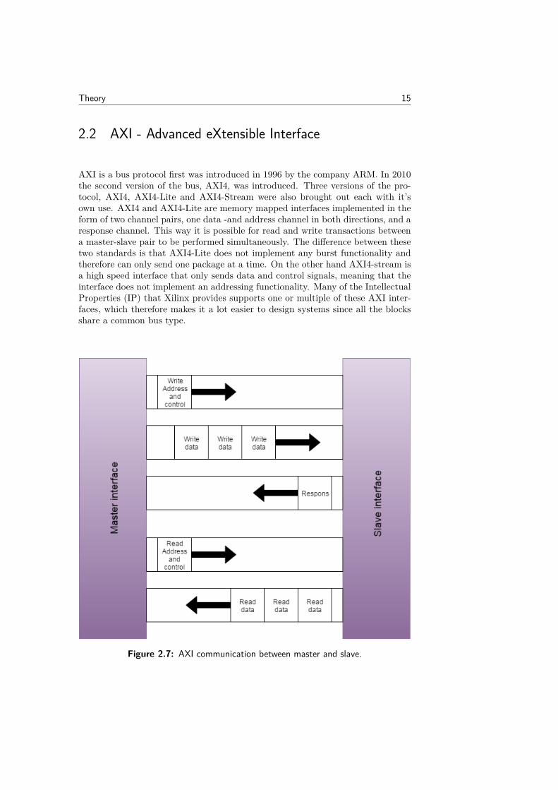
2.2 AXI - Advanced eXtensible Interface
AXI is a bus protocol first was introduced in 1996 by the company ARM. In 2010the second version of the bus, AXI4, was introduced. Three versions of the pro-tocol, AXI4, AXI4-Lite and AXI4-Stream were also brought out each with it’sown use. AXI4 and AXI4-Lite are memory mapped interfaces implemented in theform of two channel pairs, one data -and address channel in both directions, and aresponse channel. This way it is possible for read and write transactions betweena master-slave pair to be performed simultaneously. The difference between thesetwo standards is that AXI4-Lite does not implement any burst functionality andtherefore can only send one package at a time. On the other hand AXI4-stream isa high speed interface that only sends data and control signals, meaning that theinterface does not implement an addressing functionality. Many of the IntellectualProperties (IP) that Xilinx provides supports one or multiple of these AXI inter-faces, which therefore makes it a lot easier to design systems since all the blocksshare a common bus type.
Figure 2.7: AXI communication between master and slave.

16 Theory
2.2.1 Master/SlaveThe bus structure is built up by having a master and a slave. The master sendswrite- and read- requests to the slave while the slave sends responses to the master.Instead of having a header for different packages the bus has different channelsdedicated to different purposes. There are five channels: write- (W), read- (R),address write- (AW), address read- (AR) and response- (R) channel. W and Rare dedicated for data transactions while AW and AR are dedicated to addressingmemory. The R channel indicates whether or not a write was completed properly.
Write channelThe write channel has five signals: data, valid, last, keep and ready. The masteroffers one beat of data by asserting the valid signal. The data is accepted if theready signal is asserted one clock cycle when valid is high. By using last, themaster can tell the slave that the present data is the last data of the package.Keep is a byte enable signal that indicates which bytes in data are valid.
Read channelThe read channel works in the same way as the write channel except data travelsfrom slave to master. The master accepts data by asserting the ready signal, whilstvalid, last and keep tells the master which data to accept.
Address write channel and responseThere are seven signals in the AW channel: addr, valid, ready, burst, cache, len,size, lock, qos and prot. These signals describe what will be presented on the Wchannel as well as where data is stored. The master offers an address together witha description of the package by asserting the valid signal. The slave accepts theaddress by asserting ready for one clock cycle. In AXI4 the burst signal indicateswhich mode the addressing should be in, e.g. incremental as we use in this design,whilst the rest of the signals describe how to handle data. Len defines how manybeats the package carries, size is how many bytes each beat carries and cachedefines the possibility of modifying the data. To read more information on signaldeclarations please turn to Xilinx AXI reference pages [6].
Address read channelThe AR channel works similarly to the AW channel but instead of to where andhow the master tells the slave from where and how. This way we know what tosuspect from the read channel.

Chapter3System
3.1 Development tools
3.1.1 ISE project navigatorXilinx project navigator is a complete environment for the design and develop-ment of Xilinx products [7]. It provides project and design source managementand allows the user in easy steps to transverse through the FPGA design flowsuch as synthesis and place and route. ISE also provides a tool called chipscopewhich allows the user to trigger and store signal values during run time for betterdebug possibilities. After place and route has been performed a .bit file is createdcontaining all needed data to route the design on the FPGA. The program canbe run by using the command prompt in windows and can also be scripted usingTool Command Language (TCL) scripts to automate the work flow. Even thoughthis is preferred we used the graphical interface when designing.
3.1.2 iMPACTThis program is used to configure the FPGA device. The FPGA connects itsrouting net by reading the information on a Programmable Read Only Memory(PROM). This PROM is configured via the JTAG connection on the board andcan be set up by iMPACT. iMPACT uses the .bit file created in ISE to generatea .mcs file that is used to configure the PROM.
3.2 Debugging tools
3.2.1 ISim - ISE simulatorISim has been the main debugging tool used to run pre-synthesis simulations ofthe design. The tool is built into ISE and makes it possible to observe the design-generated signals in response to predefined stimuli.
17
18 System
3.2.2 QuestasimIn extension to Isim, Questasim has been used. As a third party simulator it pro-vides some extra features and behaves a little differently from the Isim simulator.The reason for using different simulators will not be covered in this report to agreat extent than explaining the lessons learned whilst using the different tools.
3.2.3 AnalyzerThis program is necessary when using Chipscope. In this program the user canconnect to the FPGAs JTAG connection, set up trigger conditions and createsignal waveforms of the sampled data. The connections on the FPGA are knownby configuring the program using an ISE generated .bit file. Waveforms can thenbe exported as value change dump (VCD) files and analyzed in e.g. Questasim.In Questasim VCD files needs to be converted to WLF files.
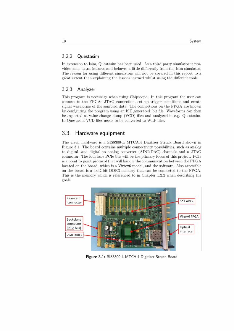
3.3 Hardware equipmentThe given hardware is a SIS8300-L MTCA.4 Digitizer Struck Board shown inFigure 3.1. The board contains multiple connectivity possibilities, such as analogto digital- and digital to analog converter (ADC/DAC) channels and a JTAGconnector. The four lane PCIe bus will be the primary focus of this project. PCIeis a point to point protocol that will handle the communication between the FPGAlocated on the board, which is a Virtex6 model, and the software. Also accessibleon the board is a 4x4Gbit DDR3 memory that can be connected to the FPGA.This is the memory which is referenced to in Chapter 1.2.2 when describing thegoals.
Figure 3.1: SIS8300-L MTCA.4 Digitizer Struck Board

Chapter4Implementation
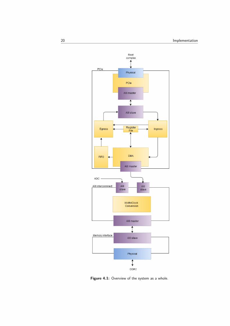
4.1 Architecture overviewIn Figure 4.1, an overview of the system is shown. All the system parts described inthis chapter are included along with an explanation of how the parts are connected.
4.2 PCI Express interfaceThe endpoint PCIe block of this project is the Virtex-6 Integrated Block for PCIExpress v2.5 [8] implemented using the IP CORE generator in ISE. This IP in-cludes an AXI4-stream interface, which comes in handy when implementing therest of the design. The IP consists of modifiable vhdl code and a black box(standard ISE component PCIE_2_0 [8]) containing the PCIe data- and physicallayers. The modifiable files consists of the AXI4-stream interface and the receive-and transmit buffers. Thus the transaction layer that handles the incoming TLPsneeds to be implemented separately. For this task two blocks are implemented;Egress is responsible for encoding outgoing TLPs and Ingress for decoding the in-coming TLPs. With these two block a user is able to write and read 32 bit wordsto a register file using write- and read requests. This register file contains controlsignals for the circuit.To access the DDR3 memory a DMA block is implementedto relieve the CPU of large data transfers. To do this the user sets up DMA reg-isters seen in table 4.1, which the DMA block uses to create either write- or readrequests to send upstream.
4.2.1 IngressThe Ingress block is the first step on the receiving side of the interface. In this blockthe headers of the incoming packages are evaluated and reactions depending onthe format and type fields of the package are generated. A TLP sent downstreamis considered to be valid if it has the format and type of a write- or read requestof 32 bits or a completion containing data to be written to DDR3 memory.
When the logic detects a start of a TLP the Finit State Machine (FSM),shown in Figure 4.2, determines the format and type of the package and triggerstransactions to corresponding states. In the write state, data and address are
19
20 Implementation
Figure 4.1: Overview of the system as a whole.

Implementation 21
decoded and sent together with a write enable signal to the internal register block.At the same time the FSM transverse into the W8_STATE. This invokes a controlsignal (write_busy) to go high, telling the FSM to wait in the W8_STATE untilthe FSM is ready to accept a new TLP. If the TLP is a read request the addressis decoded and the data is discarded. The address is sent to the register blockand FSM waits in the W8_STATE until the control signal (comp_done) indicatesthat a completion containing the right data was sent upstream before returning toRST_STATE.
Figure 4.2: FSM with transaction triggers in block Ingress
The only way that a completion can be sent downstream is if a DMA trans-action has been initiated by the CPU, in which case a read request has been sentupstream. The completion will contain the requested data and should be for-warded to the DMA unit, which will write it into memory. During transfer theFSM will lock in RECEIVE_DMA_DATA state, leaving the DMA to handle all

22 Implementation
data until the last data has been received.
4.2.2 EgressThis block is responsible for generating TLPs that will be sent upstream in re-sponse to requests from other blocks. The main objective is to create TLP headersof the outgoing data. There are three possible scenarios that can occur namely:DMA write transaction is initialized, DMA read transaction is initialized or acompletion needs to be sent as a reaction to a received read request.
Figure 4.3: FSM with transaction triggers in block Egress
DMA read requestIn RST_STATE a DMA read request will be initiated by the computer writingthe DMA WRITE CTRL register, explained in Section 4.2.3. As this happens aregister called DMA_SEL is assigned to low to clarify that a read transaction isactive, and FSM shown in Figure 4.3 switches to DMA_TRAN_H1 state. Here itwaits until valid data from memory is present in the DMA_READ_FIFO shown in

Implementation 23
Figure 4.1. Because of packet configurations in the DMA_READ_FIFO a headercan now be created knowing that data will follow continuously. A write requestTLP is created and sent upstream together with requested data. This is writtento a base address specified by the DMA READ DST registers. If the read requestslength is larger then 128 bytes, which is the maximum payload size configuredin the PCIe block, the FSM cycles back to DMA_TRAN_H1 state after sendingfirst TLP to repeat the procedure - each time adding an offset of 128 bytes to thebase address until all requested data has been written to computer memory. Asthe last package is sent an interrupt is sent to the computer to request a pollingof the IRQ Status register shown in Table 4.3.
DMA write request
Write request is mostly handled by the ingress block but needs to be initiated bysending read requests to the computer. This way the CPU does not need to initiateall transactions. In RST_STATE the FSM is waiting for DMA WRITE CTRLto be written. When this happens DMA_SEL is asserted high and FSM switchesto DMA_TRAN_H1 state where the first request header is created. FSM thenswitches to DMA_TRAN_H2 where addressing specified in DMA WRITE SRCis made before returning to RST_STATE.
Completion
If a completion is requested the block builds the first header of the completionheader and then jumps to CPL_STATE_QW1, which will combine the secondheader together with the requested data. The addressing of the register bank isdone in the RST_STATE so there is no latency loss as long as the transactionbuffer is ready.
4.2.3 Register file
This block contains registers that are available for read- and write operations fromCPU. The registers acts as control- and status registers so that the computer cankeep track of what’s happening on the hardware side of the system. The addressmapping can be read from Table 4.1 followed by an explanation of specific registers.

24 Implementation
Table 4.1: Register address mapping
Offset Access Function0x000 R Module Identifier/Firmware Version register0x010 R/W ADC Acquisition Control/Status register0x011 R/W ADC Sample Control/Status register0x020 R/W0x021 R/W0x0FF R/W Master Reset register0x120 R/W ADC ch 1 Memory Sample Start Block Address0x121 R/W ADC ch 2 Memory Sample Start Block Address... R/W0x129 R/W ADC ch 10 Memory Sample Start Block Address0x12A R/W ADC chx Sample Block Length register0x200 R/W DMA READ DST ADR LO320x201 R/W DMA READ DST ADR HI320x202 R/W DMA READ SRC ADR LO320x203 R/W DMA READ LEN0x204 R/W DMA READ CTRL0x205 R/W DMA readout Sample byte swap control0x210 R/W DMA WRITE DST ADR LO320x211 R/W DMA WRITE DST ADR HI320x212 R/W DMA WRITE SRC ADR LO320x213 R/W DMA WRITE LEN0x214 R/W DMA WRITE CTRL0x220 R/W IRQ Enable0x221 R/W IRQ Status0x222 R/W IRQ Clear0x400 R/W User defined register implementation... ...0x4FF R/W
0x000 - Module Identifier/Firmware Version register
This register is used by CPU to identify an open connection between the com-puter and the FPGA. The content is read every time CPU communicates with theFPGA.Default value: 0x83012808

Implementation 25
0x010 - ADC Acquisition Control/Status register
Writing a value of 0x1 to this register will perform an immediate sampling of theADC channel.Default value: 0x0
0x020 - Memory manual reset
This register resets the memory interface and the interconnect. This is because ofa reset problem that occurs when programming the FPGA via the PROM. Resetby writing value 0x1. Reset needs to be de-asserted by writing 0x0.Default value: 0x0
0x021 - Steady state signals
This register contains the steady state signals that validates a working design. Thebit description can be seen in Table 4.2Default values: 0x0
Table 4.2: Register 0x021 - Memory steady state signals
Bit nbr Write function Read function31 - -... ... ...2 - physical memory initialization done1 - pcie link up0 - bus master enable
0x0FF - Master register reset
Writing 0x1 to this register resets all register values to default values.Default value: 0x0
0x120 - 0x129 ADC Memory Sample Start Block Address
This register contains the start addresses of the memory where ADC channels willwrite their sample values. The user is responsible to check that the addresses donot overlap.Default values : 0x0
0x12A - ADC Sample Block Length register
This register defines the number of 256 bit blocks that will be written by eachactive ADC channel per trigger.Default value : 0x0

26 Implementation
0x200 - DMA READ DST ADR LO32This register contains lower address of the computers DMA buffer. User writesthis before every memory read request.Default value: 0x0
0x202 - DMA READ SRC ADRThis register contains the start address from which DMA will read the DDR3memory.Default value: 0x0
0x203 - DMA READ LENThis register defines the number of bytes that is requested when performing a readrequest. The user is responsible that the length and start address combined donot overlap the last address of the DDR3 memory.Default value: 0x0
0x204 - DMA READ CTRLWriting the value 0x1 to this register will initialize a read request. Be sure to writeregister 0x200 - 0x203 before initializing the transfer to get satisfying results.
0x210 - DMA WRITE SRC ADR LO32This register contains lower address of the computers DMA buffer where data thatis suppose to be written are located.Default value: 0x0
0x212 - DMA WRITE DST ADRThis register contains the base address of DDR3 memory to which the data willbe written.Default value: 0x0
0x213 - DMA WRITE LENThis register defines the number of bytes that is written when performing a writerequest. The user is responsible that the length and start address combined donot overlap the last address of the DDR3.Default value: 0x0
0x214 - DMA WRITE CTRLWriting the value 0x1 to this register will initialize a write request. The userneeds to be sure to write register 0x210 - 0x213 before initializing the transfer toget satisfying results.

Implementation 27
0x221 - IRQ statusThis register indicates when an interrupt has occurred. Table 4.3 shows the bitrepresentation of the register.
Table 4.3: Register 0x221 - IRQ status
Bit nbr Write function Read function31 - -... ... ...15 - User IRQ happend14 - DAQ Done IRQ happened14 - -... ... ...1 - Write DMA Done IRQ happened0 - Read DMA Done IRQ happened
0x222 - IRQ clearBy writing this register the user can reset and clear interrupts. Write functionalityare shown in Table 4.4
Table 4.4: Register 0x222 - IRQ clear
Bit nbr Write function Read function31 - -... ... ...15 User IRQ clear -14 DAQ Done IRQ clear -13 - -... ... ...1 Write DMA Done IRQ clear -0 Read DMA Done IRQ clear -
4.2.4 DMAIn this design the DMA is implemented as a state machine that regulates theflow of data in and out of memory. The AXI interface on the PCIe block isan AXI4-stream interface while the interconnect and memory interface has anAXI4 interface that is memory mapped. One challenge for the DMA block is totranslate between the two formats. The FSM is implemented with four states asshown in Figure 4.4. In RST_STATE the length registers are sampled at thestart of each data transfer. Data transfers are initiated by control signals fromeither ingress- or egress block. If control signals initialize a read transfer, theFSM switch to DMA_READ_TO_ROOT state in which logic constructs and

28 Implementation
sends read requests to the memory. In the meantime it also receives data fromthe interconnects read channel. When all read requests have been sent the statemachine transverses to W8_STATE. Here it holds its state until all data hasbeen received. This is managed by a counter that keeps track of the numbersof un-replied packages. When a write transaction is initialized the FSM switchesto DMA_AW_STATE in which the block generates an address based on DMAWRITE DST, shown in Table 4.1. Because of the limitation on the maximumpayload size configured in the PCIe block this design does not need to send morethan one address per write transaction. After sending the address, FSM switchesto DMA_WR_FROM_ROOT state and data is sent to the AXI interconnect.When the transfer has been made an interrupt can be generated and sent to CPU.
Figure 4.4: FSM with transaction triggers in block DMA
4.3 AXI interconnect - read/write arbiterThe AXI interconnect supports multiple functions relevant for this project’s sys-tem, such as clock rate conversion, data width conversion and arbitration. TheDDR3 memory will run at double the rate of the PCIe system and therefore theclock rate conversion is practical for this application. The interconnect supportsboth clock rate multiplication and division, in this case a 1:2 conversion is used.Since the AXI-converted data from the PCIe block have a data width of 64 bitswhile memory receives data in chunks of 256 bits, data width conversion is needed.By buffering the 64-bit data from the DMA in First In First Out (FIFO) bufferson the ports of the interconnect it is possible to up-size the data to 256 bits whichthen can be sent to the memory interface. This goes in both directions since thedata has to be downsized in the other direction when data is received from thememory, as shown in Figure 4.5 [9].

Implementation 29
Figure 4.5: Structure of the interconnect.
As described in Chapter 1.2.2, the introduction of the ADC input creates aneed for read and write arbitration. The crossbar shown in Figure 4.5 includes anread -and write arbiter which can be implemented when generating the intercon-nect core, see a simplified model of our system in 4.6. The priority of the masterdevices can be set to a normal round-robin style, which means that all of themhave the same priority, or are hard coded to a set priority.
Figure 4.6: Simple representation of the interconnect arbiter.
4.4 Memory interfaceThe memory interface that connects the on-chip design with the external DDR3memory was generated with Xilinxs MIG for Virtex6 and Spartan6. The blockwas generated in Verilog since the optional embedded AXI interface is unavailablefor VHDL implementation. Parameters needed for the interface, shown in Table4.5, were acquired from the predefined memory specification. Memory type refersto the DDR3 memory model located outside of the FPGA on the board. Thedata width is the width of the bus connected from memory interface to memory.The frequency specifies at which rate the DDR3 memory should be clocked. The

30 Implementation
burst length corresponds to the size of data bursts written to the memory. Otherparameters required to generate the memory interface, such as AXI data- andaddress width, were customized to fit with the rest of the system [10].
Table 4.5: Memory specification parameters needed for the memoryinterface.
Memory type Data width Frequency Burst lengthMT41J256M16XX-15E 64-bit 400 MHz 8
The interface block consists of three parts: an AXI controller, an user interfaceand a memory interface controller containing a physical layer to the memory, asshown in Figure 4.7.
Figure 4.7: Overview of the memory interface.
4.4.1 AXI controllerThe purpose of the AXI controller is to act as a slave to the master port of theAXI interconnect. It also handles the data conversion between the AXI- anduser interface ports. Since the memory cannot handle too big bursts of data, thecontroller is also responsible for splitting the bursts into smaller bursts of four oreight packages depending on the specification in Table 4.5.
4.4.2 User interfaceThe user interface contains two FIFO buffers in which read and write data isbuffered, making it possible to control the order in which data from memory issent back. Since read data can be obtained in a different order than in which itwas requested, this reordering is necessary.
4.4.3 Memory interface controllerThe memory interface consists of bank-, rank- and column controllers and anarbiter that is connected to the physical layer. The controllers generate commands
Implementation 31
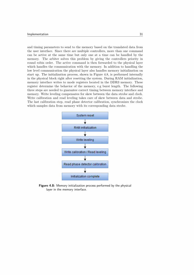
and timing parameters to send to the memory based on the translated data fromthe user interface. Since there are multiple controllers, more than one commandcan be active at the same time but only one at a time can be handled by thememory. The arbiter solves this problem by giving the controllers priority inround robin order. The active command is then forwarded to the physical layerwhich handles the communication with the memory. In addition to handling thelow level communication the physical layer also handles memory initialization onstart up. The initialization process, shown in Figure 4.8, is performed internallyin the physical block right after resetting the system. During RAM initialization,memory interface writes to mode registers located in the DDR3 memory. Theseregister determine the behavior of the memory, e.g burst length. The followingthree steps are needed to guarantee correct timing between memory interface andmemory. Write leveling compensates for skew between the data strobe and clock.Write calibration and read leveling takes care of skew between data and strobe.The last calibration step, read phase detector calibration, synchronizes the clockwhich samples data from memory with its corresponding data strobe.
Figure 4.8: Memory initialization process performed by the physicallayer in the memory interface.

32 Implementation

Chapter5Verification
Three layers of tests were performed to confirm the expected behaviour of thesystem. By following this structure, bugs were easier to find and the pace of ourwork flow increased.
5.1 Test benchBefore moving on to the actual hardware, the easiest way to debug the RegisterTransfer Language (RTL) code was to simulate with a test bench. The stimuli tothe code that was to be tested could be customized freely with a specified timing.This way corner cases could be tested without the need to navigate to the specificstate in which they occurred. To make this process as effective as possible, onlysmall blocks were tested one at a time. Otherwise, it would have been hard to findthe origins of the problems.
There were also some clear disadvantages in using test benches while debug-ging designs, such as long simulation times and test bench errors. These errorswere created by uncertainties of how the data from black boxes would look like.Examples of such boxes are the lower levels of the PCIe layers and the physicaldata from the software.
5.2 ChipscopeBy adding a Chipscope core to the ISE project it was possible to see wave formsin real-time on the FPGA. The desired trigger and data signals that were to beobserved have to be specified in the core after synthesis in ISE. The signals couldthen be examined in Analyzer after the whole design programmed onto the Virtex6.
5.3 Software testsSoftware scripts were provided at the start of the project to be able to test thesystem from a user perspective. The scripts made it possible to write and readto/from both the register file and DDR3 memory. Also, a large final test of writingand reading the whole memory from top to bottom was used to find bugs that
33

34 Verification
only appeared during large transactions. All software tests were written in C andworked as procedures to the software kernel.

Chapter6Results
Here the results are presented in two parts. One part describes how big the designgot in terms of resources and the other part describes the system performance interms of speed at the end of the project.
6.1 Design resourcesThe results from the place and route report is divided into two parts. First, shownin Table 6.1, is the device utilization. Utilization describes the amount of resourcescalculated to be used in the design, such as memories and registers. The reporteddistribution, shown in Table 6.2, describes how the resources are spread across theVirtex6. The FPGA is divided into so called slices, each containing four LUTs andeight flip-flops [11]. The number of used block RAMs are shown in Table 6.3
Table 6.1: Device utilization extracted from place and route report.
Type Amount
Slice LUT
Logic 13531 out of 80000Route-thrus 1248
Memory Dual Port RAM 3310Shift Register 985
Slice Register 24702 out of 160000
Table 6.2: Logic distribution extracted from place and route report.
Type AmountOccupied Slices 9014 out of 20000
LUT Flip Flop pairsUnused flip flop 7477 out of 29043Unused LUT 9,969 out of 29043Used LUT-FF pairs 11597 out of 29043
35

36 Results
Table 6.3: Part of specific feature utilization from place and routereport.
Type AmountRAMB36E1 21 out of 264RAMB18E1 2 out of 528
6.2 Performance6.2.1 Clock frequencyIn the design there are 7 different clock sources. The ADCs are paired into fiveclock pairs driven on different speeds. All inside the span of 100 - 130 MHz. Oursystem is driven by two clock sources. One PCIe reference clock and a systemclock. The PCIe reference clock runs at 100 MHz while the system clock runs at125 MHz. Except from these the system clock is used to create the memory clockwhich runs at 400 MHz.
6.2.2 ReadThe read functionality was calculated since the software tests were not preciseenough. The calculations were based on the fact that every package is sent con-tinuously. One package contains three headers of 32 bits and 32 blocks of data of32 bits. These packages can be sent once every 18 clock cycles, with the PCIe busclocked at 125 MHz. This gives a data transmission rate of 847 MB/s.
6.2.3 WriteThe write functionality was tested by performing a large write of the whole 2 GBmemory. The average time for one write of 2 MB was determined to 0.130 seconds.This leads to an average transmission rate of 15 MB/s.

Chapter7Analysis
This chapter goes through the thoughts and ambitions drawn from this thesis.Conclusions summarizes our thoughts, whilst future work describes what could beaccomplished with more time. Lessons learned describes problems encountered andhow they were solved, providing the reader with the knowledge to not duplicatethe same mistakes.
7.1 ConclusionsLooking back at the goals, described in Section 1.2.2, all of the parts planned forbuild were completed. In addition, read/write arbitration is working and thereforecompletes the optional, final goal. That said, although the results are satisfying,the working process did not work out as planned in the goals. The main reasoncan be attributed to our decision of using the AXI interface, which meant thatwe could not test our components with the pre-existing blocks since they wereincompatible. On the other hand, this also accelerated the development of thearbiter goals since the AXI interconnect has an easy to implement arbiter.
When observing the results, shown in Chapter 6, the read functions are about56 times faster than the writes. This is to be expected for reasons further de-scribed in Section 7.4. The reads are more relevant since the ADCs are the mainparts writing to memory, which also makes the overall results satisfying. Whencomparing the results to the original version we have found that we have the sameperformance.
A PCIe interface with our specifications, a 4x lane width and 2.5 Giga Transfersper second, has a maximum transfer speed of 1GB/s. Because of protocol overheadand delays a part of the transfer speed is lost as shown in the result of 847 MB/s ofthe read calculations shown in Section 6.2. Generally the theoretical throughputof the link can be calculated with equation 7.1, where PL is the payload size, OVthe protocol overhead, N the number of lanes and G is a parameter dependent onwhat generation/version of the protocol is used [13].
ThroughputT HEO = PL
PL + OV· N · G · (250MB/s) (7.1)
37

38 Analysis
7.2 Lessons LearnedChipscopeChipscope proved to be a powerful tool during the debugging process, although itsometimes was hard to handle. To find all relevant signals was not always possiblesince, as mentioned in Chapter 5.2, Chipscope is inserted into the work flow aftersynthesis. The chosen signals could be gone since the design has been optimizedduring synthesis. To solve this problem a keep attribute had to be introduced andapplied to the desired signals in the RTL code.
IsimAfter using a lot of test benches, both self written and predefined by Xilinx, wehave had a lot of problems with Isim. Most of the problems have been workedaround by changing computer or by specifying the wave file which is going to berun in ISE before even launching Isim. These problems were hard to predict andfind workarounds for. Later on in the project we switched simulation program toQuestasim which was a lot easier to handle. Questasims .do file is also a lot easierto handle and more versatile then Isims .wfcg which only configures waveforms.
IP coresThe IPs that Xilinx offers, such as the AXI interconnect or PCIe interface, haveshown to possess a lot of features of which not all are supported for all scenarios.One of these features is the PCIe interfaces option to obtain bus master statusthrough accessing the configuration ports. This bus mastering process was partof the old version of PCI and are nowadays resolved internally in the PCIe blockwithout the need for user interference. A lot of these details were resolved simplyby putting more time into reading the documentation.
Because of the high simulation time for DDR3 memory and the lack of softwareside on the PCIe interface we built our own simulation modules for these blocks.By doing this we missed some key features that did not work in practice e.g.memory not sending continuous packages and the PCIe block not being able toreceive discontinuous packages.
VHDL/VerilogOur preferred writing language when the project was started was VHDL. When westarted to import some of Xilinx’s IPs we realised that not all of the implementationoptions that existed for Verilog, were present for the same block in VHDL. Anexample is the AXI connectivity option for the memory interface, which onlycould be chosen in Verilog. This resulted in us learning a lot more about Verilogbut also about how a multiple language hierarchy is allowed to be constructed. Ifthe top layers of the design are made in VHDL and a sub block is implementedin Verilog, no sub block of the Verilog code is allowed to be written in VHDL, asshown in Figure 7.1a and 7.1b. This created a problem when the memory interfaceneeded to be implemented in Verilog to get access to the AXI interface. ISE needs

Analysis 39
to be set to have preference language Verilog for this to work, which made the restof the source code to violate the hierarchy structure. This was fixed by generatingthe Verilog code in a new project, enabling us to extract the source code and thenadd it to the current working project.
(a) Correct
(b) Incorrect
Figure 7.1: Illustration of correct/incorrect RTL code hierarchy.
AXI interconnect
The AXI interconnect core was one of the main blocks in our design. It providedmany of the features we needed such as clock- and width conversion and arbitra-tion. One disadvantage was the fact that it did all these things. It is harder todebug a design when it is not your own and you need to rely on documentationto get a working design. We came to the conclusion that a feature called pack-aging, which was supposed to wait to release data until whole packages had beenreceived, was needed. This was only working properly on the write channel. Theproblem lead to timing problems on the read channel, when memory did not sendcontinuous data. This was fixed by inferring an extra FIFO between the DMAand Egress, which stacked packages into continuous chunks before transforminginto TLPs.
Modifying memory command sequence
Nothing works as intended. That is one of the main lessons we have learned. Inthe best of worlds you need to generate a IP core and then its plug and play. Inthis case the memory interface used a chip select signal to disconnect the DDR3memory. This signal was grounded on the Printed Circuit Board and therefore the
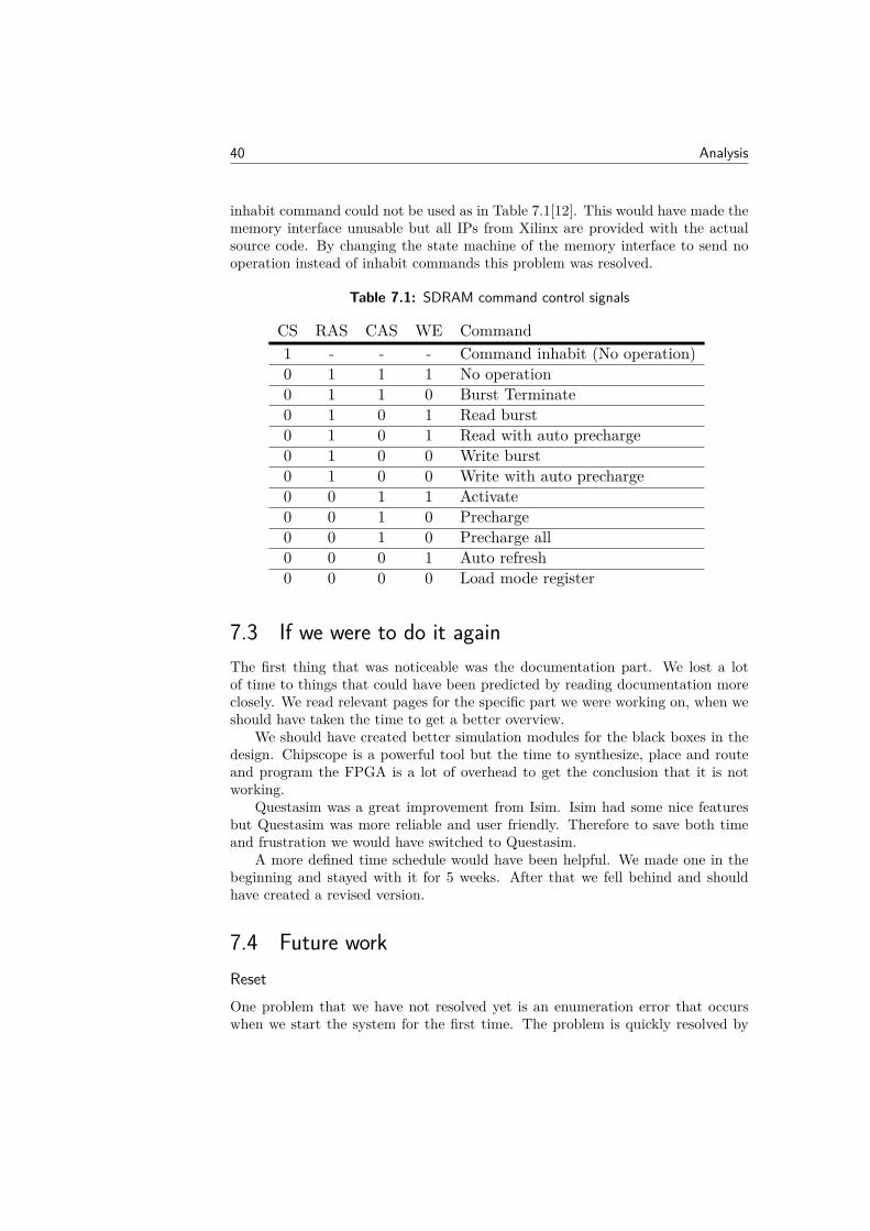
40 Analysis
inhabit command could not be used as in Table 7.1[12]. This would have made thememory interface unusable but all IPs from Xilinx are provided with the actualsource code. By changing the state machine of the memory interface to send nooperation instead of inhabit commands this problem was resolved.
Table 7.1: SDRAM command control signals
CS RAS CAS WE Command1 - - - Command inhabit (No operation)0 1 1 1 No operation0 1 1 0 Burst Terminate0 1 0 1 Read burst0 1 0 1 Read with auto precharge0 1 0 0 Write burst0 1 0 0 Write with auto precharge0 0 1 1 Activate0 0 1 0 Precharge0 0 1 0 Precharge all0 0 0 1 Auto refresh0 0 0 0 Load mode register
7.3 If we were to do it againThe first thing that was noticeable was the documentation part. We lost a lotof time to things that could have been predicted by reading documentation moreclosely. We read relevant pages for the specific part we were working on, when weshould have taken the time to get a better overview.
We should have created better simulation modules for the black boxes in thedesign. Chipscope is a powerful tool but the time to synthesize, place and routeand program the FPGA is a lot of overhead to get the conclusion that it is notworking.
Questasim was a great improvement from Isim. Isim had some nice featuresbut Questasim was more reliable and user friendly. Therefore to save both timeand frustration we would have switched to Questasim.
A more defined time schedule would have been helpful. We made one in thebeginning and stayed with it for 5 weeks. After that we fell behind and shouldhave created a revised version.
7.4 Future workResetOne problem that we have not resolved yet is an enumeration error that occurswhen we start the system for the first time. The problem is quickly resolved by

Analysis 41
restarting the enumeration process one time. A similar problem occurs in thememory interface once the system starts, where the DDR3 memory initializationprocess does not finish. Here also, the problem is resolved by an extra reset. Com-bining these two problems concludes that there probably is an error somewhere inthe reset logic.
ADCThe extra ADC inputs to the interconnect have been simulated and tested. Theconcept has been proven to work, although with some errors and not with the fullamount of ADCs. To complete this part of the project not only in simulation orin an incomplete test environment would clearly be the next step forward.
DMA writeThe solution when writing data to memory can be updated into a faster version.As it works today the computer is only able to write 64 bytes to memory at a time.After that one must update the DMA registers and start again. What should bepossible is to write the registers once with a large length. This would have madethe design faster and is definitely worth implementing.
The problem with the fast implementation is that the hardware has no controlover how completions is sent back after read requests has been sent upstream.Completions can be received with different lengths and can be reordered. Thereordering would need to be handled by applying unique tags to the read requests.This means that the completions would also have the unique tags and could havebeen ordered in that manner. Combining the completers byte count- and lengthfield, refereed to in section 2.1.5, can be used to determine how many byte is left ofa completion and how large the current package is. This would have been helpfulwhen stacking data before sending it to the DDR3 memory.
Maximum payload sizeLooking at the configurations of the PCIe block, a possibility of increasing themaximum payload size is possible. As of today it is set to be 128 bytes while thelimit is at 1024 bytes. The burst length of the AXI interface has a maximum of256 QW which is at most is a payload size of 2048 bytes. This means that if thePCIe maximum payload size would increase the AXI interfaces in the design wouldstill be able to cope with the data sizes. This would have increased the speed ofthe system as well as minimized the number of addresses sent to the memory.

42 Analysis

References
[1] ESS homepage,https://web.archive.org/web/20140517050510/http://europeanspallationsource.se/,August 2014
[2] ESS Technical Design Report 2013,http://docdb01.esss.lu.se/DocDB/0002/000274/015/TDR_online_ver_all.pdf,January 2016
[3] F. Qiua, J. Gaoa, H. Lina, R. Liua, X. Maa, P. Shaa, Y. Suna, G. Wanga,Q. Wanga, B. Xua, R. Zengc,"A new IQ detection method for LLRF", Sci-enceDirect, vol 675, pp. 139-143, 2012
[4] Ravi Budruk, Don Anderson and Tom Shanley,PCIe Express System Architecture,MindShare INC, First Edition, 2003
[5] PCI Express 2.0 base specification,http://read.pudn.com/downloads95/ebook/383403/PCI_Express_Base_Specification_v20.pdf,January 2016
[6] AXI reference guide,http://www.xilinx.com/support/documentation/ip_documentation/ug761_axi_reference_guide.pdf,November 2015
[7] ISE project nevigator product description,http://www.xilinx.com/tools/projnav.htm,January 2016
[8] User guide for Xilinx PCIe core,http://www.xilinx.com/support/documentation/ip_documentation/v6_pcie/v2_5/ug671_V6_IntBlock_PCIe.pdf,January 2016
43

44 References
[9] AXI interconnect product description,http://www.xilinx.com/products/intellectual-property/axi_interconnect.html,November 2015
[10] Xilinx Memory Interface Generator product description,http://www.xilinx.com/products/intellectual-property/mig.html,October 2015
[11] Virtex-6 Family Overview,http://www.xilinx.com/support/documentation/data_sheets/ds150.pdf,January 2016
[12] Command table for DDR3 SDRAM,http://www.intel.com/content/dam/www/public/us/en/documents/datasheets/nanya-nt5ds-datasheet.pdf#page=13,January 2016
[13] L. Rota, M. Caselle, S. Chilingaryan, A. Kopmann, M. Weber, "A new DMAPCIe Architecture for Gigabyte Data Transmission", Real Time Conference(RT), pp. 1-2, 2014

Hig
h Sp
eed B
ackbo
ne fo
r FPGA
at ESS
Department of Electrical and Information Technology, Faculty of Engineering, LTH, Lund University, 2016.
High Speed Backbone forFPGA at ESS
Max AnderssonGabriel Jönsson
Series of Master’s thesesDepartment of Electrical and Information Technology
LU/LTH-EIT 2016-482
http://www.eit.lth.se
Ma
x An
de
rsson
& G
abriel Jö
nsso
n
Masters’s Thesis