high resolution electrochemical stm: new structural...
TRANSCRIPT

Available online at www.sciencedirect.comJournal of
www.elsevier.com/locate/jelechem
Journal of Electroanalytical Chemistry 613 (2008) 118–124
ElectroanalyticalChemistry
High resolution electrochemical STM: New structural results forunderpotentially deposited Cu on Au(111) in acid sulfate solution
Natasa Vasiljevic a,*, Lasantha T. Viyannalage b, Nikolay Dimitrov b, Karl Sieradzki c
a Sandia National Laboratories, P.O. Box 5800, MS 1415, Albuquerque, NM 87185-1415, USAb Department of Chemistry, SUNY-Binghamton, P.O. Box 6000, Binghamton, NY 13902-6000, USA
c Ira A. Fulton School of Engineering, Arizona State University, P.O. Box 876106, Tempe, AZ 85287-6106, USA
Received 31 July 2007; received in revised form 14 October 2007; accepted 22 October 2007Available online 30 October 2007
Abstract
Adsorption of sulfate assists Cu monolayer underpotential deposition (upd) on Au(111) in a unique way, rendering two distinct struc-tural stages: (i) formation of a low-density Cu phase at coverage of 2/3 ML known as the
ffiffiffi3p�
ffiffiffi3p� �
R30� or honeycomb phase; (ii) for-mation of a complete monolayer, i.e., Cu-(1 · 1) phase pseudomorphic with respect to underlying Au(111) substrate. In this paper wepresent new structural in situ scanning tunneling microscopy (STM) results for this system. We show and discuss the STM imaging of thecopper honeycomb superstructure probed underneath the co-adsorbed
ffiffiffi3p�
ffiffiffi3p� �
R30� sulfate adlayer in the low-density phase. Highresolution imaging during the phase transition from the low to high density copper phase unambiguously shows the existence of anordered sulfate structure p(2 · 2) on the pseudomorphic Cu-(1 · 1) layer. The new structure is seen during the co-existence of two copperphases as well as upon completion of the Cu-(1 · 1) monolayer. While supported by earlier chronocoulometric measurements in the samesystem, the new structural results raise questions that need to be addressed in a future work.� 2007 Elsevier B.V. All rights reserved.
Keywords: In situ scanning tunneling microscopy; Underpotential deposition; Copper, Au(111); Sulfate; Anion adsorption
1. Introduction
The fascination with the Cu underpotential deposition(upd) system on Au(1 11) in sulfate is far from over. Dur-ing the last two decades this has undoubtedly been themost studied system and is considered as an archetypefor metal upd. It has been characterized by almost all ana-lytical techniques used in modern electrochemical surfacescience [1]. The summary of both ex situ and in situ analyt-ical and structural studies on Cu/Au(111) can be found ina recent review by Herrero et al. [1]. Almost all newlydeveloped or adapted in situ structure-sensitive techniquesin electrochemistry were introduced by or employed instudies of this system [2–9]. The wealth of results relatedto the behavior and structural characteristics renders the
0022-0728/$ - see front matter � 2007 Elsevier B.V. All rights reserved.
doi:10.1016/j.jelechem.2007.10.021
* Corresponding author. Tel.: +1 505 844 0566; fax: +1 505 844 1197.E-mail address: [email protected] (N. Vasiljevic).
Cu upd layer on Au(1 11) in sulfate solution an excellentcandidate for theoretical modeling. The unique phase tran-sition aspects of this system warranted its choice as a pro-totype for which the first statistical mechanics lattice-gasmodel for upd systems was developed by Blum and Hick-aby [10–12]. This theoretical work was extended later usingMonte Carlo (MC) simulations, Rikvold et al. [13,14].Dynamic MC simulations [15] were also employed toreproduce the experimentally obtained current transientsshedding more light on the kinetic aspects of surface phasetransitions taking place in that system [16].
Among the variety of upd systems, Cu on Au(111) insulfate solution is unique with well-defined structuralstages of monolayer formation governed by the co-adsorp-tion of sulfate ions. These stages are clearly represented bycyclic voltammetry features (Fig. 1a) and interpreted bynumerous experimental and theoretical studies: (i) the cop-per deposition starts by formation of a random lattice gas
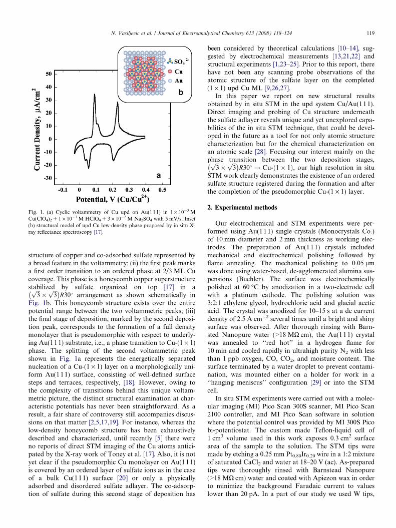
Fig. 1. (a) Cyclic voltammetry of Cu upd on Au(111) in 1 · 10�3 MCu(ClO4)2 + 1 · 10�3 M HClO4 + 3 · 10�2 M Na2SO4 with 5 mV/s. Inset(b) structural model of upd Cu low-density phase proposed by in situ X-ray reflectance spectroscopy [17].
N. Vasiljevic et al. / Journal of Electroanalytical Chemistry 613 (2008) 118–124 119
structure of copper and co-adsorbed sulfate represented bya broad feature in the voltammetry; (ii) the first peak marksa first order transition to an ordered phase at 2/3 ML Cucoverage. This phase is a honeycomb copper superstructurestabilized by sulfate organized on top [17] in affiffiffi
3p�
ffiffiffi3p� �
R30� arrangement as shown schematically inFig. 1b. This honeycomb structure exists over the entirepotential range between the two voltammetric peaks; (iii)the final stage of deposition, marked by the second deposi-tion peak, corresponds to the formation of a full densitymonolayer that is pseudomorphic with respect to underly-ing Au(11 1) substrate, i.e., a phase transition to Cu-(1 · 1)phase. The splitting of the second voltammetric peakshown in Fig. 1a represents the energetically separatednucleation of a Cu-(1 · 1) layer on a morphologically uni-form Au(1 11) surface, consisting of well-defined surfacesteps and terraces, respectively, [18]. However, owing tothe complexity of transitions behind this unique voltam-metric picture, the distinct structural examination at char-acteristic potentials has never been straightforward. As aresult, a fair share of controversy still accompanies discus-sions on that matter [2,5,17,19]. For instance, whereas thelow-density honeycomb structure has been exhaustivelydescribed and characterized, until recently [5] there wereno reports of direct STM imaging of the Cu atoms antici-pated by the X-ray work of Toney et al. [17]. Also, it is notyet clear if the pseudomorphic Cu monolayer on Au(1 11)is covered by an ordered layer of sulfate ions as in the caseof a bulk Cu(111) surface [20] or only a physicallyadsorbed and disordered sulfate adlayer. The co-adsorp-tion of sulfate during this second stage of deposition has
been considered by theoretical calculations [10–14], sug-gested by electrochemical measurements [13,21,22] andstructural experiments [1,23–25]. Prior to this report, therehave not been any scanning probe observations of theatomic structure of the sulfate layer on the completed(1 · 1) upd Cu ML [9,26,27].
In this paper we report on new structural resultsobtained by in situ STM in the upd system Cu/Au(11 1).Direct imaging and probing of Cu structure underneaththe sulfate adlayer reveals unique and yet unexplored capa-bilities of the in situ STM technique, that could be devel-oped in the future as a tool for not only atomic structurecharacterization but for the chemical characterization onan atomic scale [28]. Focusing our interest mainly on thephase transition between the two deposition stages,ffiffiffi
3p�
ffiffiffi3p� �
R30� ! Cu-ð1� 1Þ, our high resolution in situSTM work clearly demonstrates the existence of an orderedsulfate structure registered during the formation and afterthe completion of the pseudomorphic Cu-(1 · 1) layer.
2. Experimental methods
Our electrochemical and STM experiments were per-formed using Au(1 11) single crystals (Monocrystals Co.)of 10 mm diameter and 2 mm thickness as working elec-trodes. The preparation of Au(1 11) crystals includedmechanical and electrochemical polishing followed byflame annealing. The mechanical polishing to 0.05 lmwas done using water-based, de-agglomerated alumina sus-pensions (Buehler). The surface was electrochemicallypolished at 60 �C by anodization in a two-electrode cellwith a platinum cathode. The polishing solution was3:2:1 ethylene glycol, hydrochloric acid and glacial aceticacid. The crystal was anodized for 10–15 s at a dc currentdensity of 2.5 A cm�2 several times until a bright and shinysurface was observed. After thorough rinsing with Barn-sted Nanopure water (>18 MX cm), the Au(11 1) crystalwas annealed to ‘‘red hot’’ in a hydrogen flame for10 min and cooled rapidly in ultrahigh purity N2 with lessthan 1 ppb oxygen, CO, CO2, and moisture content. Thesurface terminated by a water droplet to prevent contami-nation, was mounted either on a holder for work in a‘‘hanging meniscus’’ configuration [29] or into the STMcell.
In situ STM experiments were carried out with a molec-ular imaging (MI) Pico Scan 300S scanner, MI Pico Scan2100 controller, and MI Pico Scan software in solutionwhere the potential control was provided by MI 300S Picobi-potentiostat. The custom made Teflon-liquid cell of1 cm3 volume used in this work exposes 0.3 cm2 surfacearea of the sample to the solution. The STM tips weremade by etching a 0.25 mm Pt0.80Ir0.20 wire in a 1:2 mixtureof saturated CaCl2 and water at 18–20 V (ac). As-preparedtips were thoroughly rinsed with Barnstead Nanopure(>18 MX cm) water and coated with Apiezon wax in orderto minimize the background Faradaic current to valueslower than 20 pA. In a part of our study we used W tips,

120 N. Vasiljevic et al. / Journal of Electroanalytical Chemistry 613 (2008) 118–124
made by etching 0.25 mm wire in 1 M NaOH solution at 8–10 V (ac). The stability and the performance of W tips wasenhanced by electrodeposition of Au on to the tip from asolution 5 · 10�4 M HAuCl4 in a 1:3 mixture of HCl andethylene glycol. A copper wire served as a reference elec-trode and a platinum wire was used as a counter electrodein all experiments. All potentials are reported with respectto Cu2+/Cu pseudo reference electrode (PRE). The work-ing solution was 1 · 10�3 M Cu(ClO4)2 (ALFA Aesar,99.999%) + 1 · 10�3 M HClO4 (GFS chemicals, doubledistilled) + 3 · 10�2 M Na2SO4 (ALFA Aesar, Puratron-ic�, 99.9955%).
3. Results and discussion
3.1. Low-density phase
Due to the unique surface structure of the Cu upd low-density phase, the interpretation of relevant in situ STMand AFM results [2,9,19] has historically created confu-sion. In fact, these results were in general disagreementwith the structures considered theoretically [10–14], con-cluded from ex situ LEED and RHEED studies [30] anddetermined by in situ EXAFS [24] studies. The atomicstructure that is readily observable by scanning probemicroscopy (SPM) techniques is
ffiffiffi3p�
ffiffiffi3p� �
R30� [2,9,19].The maxima observed in STM and AFM images, as clearlyseen in Fig. 2a, initially were considered to be Cu atoms.While this conclusion was the most intuitive one, no plau-sible explanation was found as to why these Cu atomswould account only for 1/3 ML coverage instead of 2/3ML as determined by chronocoulometry [21,22] andquartz-crystal microbalance measurements [31,32]. Thisissue was resolved by an in situ X-ray scattering [17] thatproposed the structural model presented in Fig. 1b.According to this model, it was suggested that all resultsfrom SPM techniques [2,9,19] typically show sulfate mole-cules that sit in
ffiffiffi3p�
ffiffiffi3p� �
R30� positions above the planeof a copper honeycomb layer. The bonding in this config-uration is provided by three oxygen atoms connected withneighboring copper atoms while the fourth oxygen atom
Fig. 2. In situ STM images of low-density phase at a potential of 0.15 V obtasulfate
ffiffiffi3p�
ffiffiffi3p� �
R30� structure obtained with a tip bias B1 = 30 mV; (b) copimage showing the reproducibility of the observed structure as the bias is cha
from the sulfate ion points out above the plane of Cuatoms [17]. In turn, copper atoms from the low-densitystructure occupy threefold sites on the underlyingAu(111) surface thus forming the honeycomb structure.Characterized that way, the low-density Cu upd layer onAu(111) in sulfate solution is undoubtedly a complex sur-face superstructure that belongs to a class of sandwichstructures where an adlayer is accompanied by a co-adsorbed on top anion layer. It has been previously demon-strated that such structures could be imaged selectively bycareful manipulation of STM tunneling conditions e.g. tun-neling current, or tip potential (tip bias) [20,33]. It has alsobeen demonstrated that metal deposition on the tip cangreatly improve the quality and stability of imaging atatomic scales [26]. For this reason we used gold-coatedW tips. In these experiments we probed the structure ofthe Cu layer underneath the sulfate by manipulating thetip potential and switching the sign of the tip bias. Resultsof this approach are shown in Fig. 2 where first two imagesobtained at constant tunneling current illustrate howswitching of the bias polarity changes the STM imagingof the normally observed
ffiffiffi3p�
ffiffiffi3p� �
R30� sulfate structure(Fig. 2a) to the imaging of the usually ‘‘hidden’’ Copperhoneycomb structure (Fig. 2b). This result is quite repro-ducible as shown in Fig. 2c. Switching the bias alternatelyduring scanning in that case caused the sulfate structure toreappear and disappear accordingly. A possible cause forthis imaging selectivity could be associated with the tipmaterial that is identical to the substrate. An appropriatelychosen tip potential generates low-density structure of Cuupd on the tip surface, whereas switching the sign of thebias voltage influences the tunneling conditions and imag-ing quality.
The nucleation of the low-density phase within the timescale of an STM scan (�seconds) is ‘‘instantaneous’’. Ran-dom nucleation is followed by growth of equivalent trans-lational domains of the
ffiffiffi3p�
ffiffiffi3p� �
R30� phase resulting information of domain walls appearing as brighter coloredlines on the STM images. The kinetics details offfiffiffi
3p�
ffiffiffi3p� �
R30� phase formation and stabilization arethoroughly described in the study of Xia et al. [34]. Once
ined with different bias sign, i.e., tip potentials. Images size 6 · 6 nm: (a)per honeycomb structure obtained with a tip bias B2 = �30 mV; (c) STMnged (as marked) during imaging scan.

N. Vasiljevic et al. / Journal of Electroanalytical Chemistry 613 (2008) 118–124 121
formed, the domain network coarsens with time, i.e., thesmaller domains disappear at the expense of larger oneswhat is typically observed within a few minutes of polariza-tion [34]. Our high resolution STM images of the domainsfollowing coarsening and stabilization show ‘‘super-heavy’’domain wall structures consistent with the STMresults of Xia et al. [34], Fig. 3. The so-called superheavywalls are characterized by a close packed (1 · 1) localarrangement of sulfate molecules as shown in Fig. 3.Fig. 3a shows the intersection of three
ffiffiffi3p�
ffiffiffi3p� �
R30�
translational domains of the sulfate structure. For the sakeof clarity Fig. 3b shows the domains schematically (equiv-alent to Fig. 3a in Xia et al. [34]). An important feature thatfollows low-density phase formation is the appearance ofislands not present at all on the bare Au(111) surfacebefore Cu deposition. These islands form owing to excessatoms resulting from the lifting of the 22�
ffiffiffi3p� �
Au(1 11) surface reconstruction [34]. They slowly disappearafter complete stripping of the Cu upd layer at more posi-tive potentials.
3.2. Phase transition betweenffiffiffi3p�
ffiffiffi3p� �
R30� and Cu-
(1 · 1)
The transition fromffiffiffi3p�
ffiffiffi3p� �
R30� to Cu-(1 · 1) phasewas followed by incrementing the potential in 3–5 mV stepsto increase the Cu coverage. Characteristic morphologyfeatures observed during such slow Cu-(1 · 1) monolayerformation are presented in Fig. 4. Starting from a potentialof 0.1 V, i.e., at the onset of the second cathodic peak, thedomain walls appear much more pronounced in STMimages, as shown in Fig. 4a. This appearance is due to asubstantial increase of their width. Based on the surfacestructures obtained at these three different polarizationpotentials (emphasizing nucleation (Fig. 4a), growth(Fig. 4b) and completion (Fig. 4c) of Cu-(1 · 1) monolayer)we can clearly characterize this transition as an ‘evolution’of the domain wall network formed in the low-densityphase. As mentioned above, the superheavy walls serve asnucleation sites of the Cu-(1 · 1) phase. The initial growthis quasi one-dimensional as the domain walls grow in width
Fig. 3. (a) High resolution STM image of three intersecting equivalent translati20 · 20 nm; (b) schematic illustration of domains intersection as in (a) where tcorresponding sulfate molecules. (For interpretation of the references in colour
forming a very uniform network of Cu-(1 · 1) domains asshown in Fig. 5a (illustrating a network of uniform domainwalls with a width of �5 nm). At lower underpotentials,the regions of Cu-(1 · 1) become less uniform and theirgrowth may be characterized as two-dimensional. Largerdomains of Cu-(1 · 1) phase start evolving at triple junc-tions of the original domain wall network. In the courseof this two-dimensional growth the Cu-(1 · 1) domainsinteract with each other and coarsening takes place, even-tually as a result of the two co-existing phases reachingan equilibrium structure shown in Fig. 5b. Therefore the‘template’ of the initially present domain wall networkbecomes less and less recognizable in the phase transitionprocess.
The atomistic mechanism of Cu-(1 · 1) monolayer for-mation assumes displacement of sulfate anions fromffiffiffi
3p�
ffiffiffi3p� �
R30� positions and filling of the ‘emptied’ three-fold positions by copper atoms. Electrochemical (chrono-coulometric) measurements [21,22], theoreticalconsiderations [10–14] and most recently in situ surfacestress measurements [4,5] rationalize that the sulfate anionsshould most likely be co-adsorbed again on top of the Cu-(1 · 1) phase. However, to date reported SPM results donot support this conclusion and thus contribute to thepre-existing controversy. Both STM [26,34,35] and AFM[9,27] studies report on the ‘bare’ atomic structure of thecompleted Cu adlayer with an atomic spacing of the under-lying Au(1 11) which is attributed to Cu-(1 · 1) layer. Actu-ally, there are not that many studies of the Cu upd processfocusing on this aspect of monolayer formation in contrastto the numerous reports and analysis of the low-densitystructure that is so easily observable. In the AFM study,Manne et al. [9] express concern about the reported resultbecause of the ‘missing’ sulfate adlayer on the completedCu monolayer. There is a possibility of probe shieldingand/or screening effects that could result in disorganizationand/or removal of the sulfate adlayer during imaging. Thesame reasoning could explain why most of the STM studiesreport imaging of the Cu-(1 · 1) structure, albeit there isonly one report that shows an actual STM image of it[26]. Therefore this issue requires further investigation
onal domains offfiffiffi3p�
ffiffiffi3p� �
R30�phase at a potential of 0.125 V. Image sizehree equivalent translational domains are marked with different colors ofin this figure legend, the reader is referred to the web version of this article.)

Fig. 4. In situ STM images of surface structures during transition fromffiffiffi3p�
ffiffiffi3p� �
R30� to Cu-(1 · 1) phase taken at different polarization potentials.Images size 500 · 500 nm: (a) a pronounced appearance of domain wall network as the potential changes negatively from a potential of 0.1–0.095 V. Thearrow points in the direction of STM scan and the dotted line marks moment of the potential step during the scan; (b) evolution of Cu-(1 · 1) domains atpotentials 0.06 V and (c) 0.03 V.
Fig. 5. In situ STM images showing growth of Cu-(1 · 1) domain networkduring phase transition. Images size 200 · 200 nm: (a) polarizationpotential 0.08 V; (b) polarization potential 0.05 V.
122 N. Vasiljevic et al. / Journal of Electroanalytical Chemistry 613 (2008) 118–124
and clarification. We focused our attention on the phasetransition from the low to high density copper layer andon the possibility to atomically resolve the phase transition.
Our high resolution STM results show the presence ofan ordered anion structure on the completed pseudomor-phic Cu-(1 · 1) layer. Fig. 6a obtained at constant heightmode shows an atomic resolution image involving two co-existing phases. Resolved simultaneously are two perfecthexagonal structures featuring different atomic spacingand rotated with respect to each other by 30�, i.e., maindirections of two superstructures are orthogonal withrespect to each other. Fig. 6b and c are selected regionsthat are used to compare the two atomically resolvedstructures. Based on the Fourier transform analysis inFig. 6b, the lower contrast regions represent theffiffiffi
3p�
ffiffiffi3p� �
R30� phase with a unit cell spacing ofa1 = 4.9 ± 0.2 A, i.e., a1 ¼
ffiffiffi3p
aAu. The second co-existingregion with the higher electronic contrast represents agrowing Cu-(1 · 1) phase that has a larger unit cell sizeof a2 = 5.6 ± 0.2 A corresponding to a2 = 2aAu. HereaAu is the nearest neighbor spacing of underlyingAu(1 11) substrate. This analysis suggests that the struc-ture of the anion adlayer on Cu-(1 · 1) phase is a
p(2 · 2) structure. The same p(2 · 2) structure is observedupon complete formation of Cu-(1 · 1) monolayer. Sev-eral different surface spots were monitored to ascertainthe sulfate adlayer structure and thus to exclude any pos-sibility of tip shielding effects or other imaging artifacts.We must note that all our high resolution STM imagesshow anion p(2 · 2) structure (with the spacing twice thespacing of Au) organized on the top of the pseudomor-phic Cu-(1 · 1) layer (with the spacing same as Au). How-ever we were unable to image directly Cu-(1 · 1) layer,i.e., to probe under the anion adlayer.
This new finding suggests the presence of a differentstructure for sulfate adlayer on the completed copper layer.Imaging of both anion structures at the same time shown inFig. 6 allows for unambiguous comparison and determina-tion of the structural relationships. This result is in contra-diction to in situ surface X-ray diffraction (SXD) results byNakamura et al. [25] who suggested that the
ffiffiffi3p�
�ffiffiffi3pÞR30� sulfate structure remains unchanged after comple-
tion of the Cu upd layer. It is possible that the SXD result[25] can be attributed to the potentiodynamically per-formed in situ measurements that likely did not allow forenough time for the system to complete the transitionbetween anion structures observed in our experiments.Our result showing structural evolution of the anion layerfrom the honeycomb to a full copper layer is supportedby earlier coulometric measurements for the same system[22] suggesting a substantial decrease in the sulfate cover-age upon completion of the Cu-(1 · 1) layer. While Shiand Lipkowski [22] clearly state that the loss of SO2�
4 ionsbrings the coverage down to a value close to 0.2 ML that inturn is close to the coverage for sulfate absorption on bareAu(111) that yields
ffiffiffi3p�
ffiffiffi7p� �
R30� structure. Sulfate ionsare also known to organize in a so-called
ffiffiffi3p�
ffiffiffi7p� �
R30�
configuration on bare Cu(111) [20]. Why the structureobserved in our experiments expands from
ffiffiffi3p�
� ffiffiffi3pÞR30�
to p(2 · 2) maintaining the system symmetry remainsunclear and is yet to be addressed further by modelingand simulation work.

Fig. 6. (a) High resolution in situ STM image 20 · 20 nm obtained in constant height mode showing the atomic structure of two co-existing phases(marked by arrows) at a potential of 0.05 V. The two atomic structures are hexagonal and rotated 30� with respect to each other. Images (b) and (c) areinsets of 4.5 · 4.5 nm size within each phase; (b) atomic structure with the unit cell size a1 ¼
ffiffiffi3p
aAu ¼ ð4:9� 0:2Þ A, i.e.,ffiffiffi3p�
ffiffiffi3p� �
R30� low-densityphase; (c) atomic structure with the unit cell size a2 = 2aAu = (5.6 ± 0.2) A is the p(2 · 2) structure of sulfate layer on Cu-(1 · 1) phase.
N. Vasiljevic et al. / Journal of Electroanalytical Chemistry 613 (2008) 118–124 123
4. Summary
This work presents structural results of copper upd onAu(1 11) in sulfate solution revealing structural aspectsand features that have not been reported previously.By adjusting the voltage of Au-coated STM tips we wereable to image the low-density copper honeycomb struc-ture at intermediate underpotentials. We were also ableto observe triple junctions associated with the threeequivalent rotational domains of the low-density
ffiffiffi3p�
�ffiffiffi3pÞR30� phase. Finally, we report the co-existence offfiffiffi3p�
ffiffiffi3p� �
R30� and p(2 · 2) sulfate layers during thephase transition. More work is needed to understandthe issues associated with the formation of the p(2 · 2)sulfate adlayer phase on the Cu-(1 · 1) ML/Au(111) withrespect to a
ffiffiffi3p�
ffiffiffi7p� �
R30� phase which is reported forelemental close packed hexagonal faces of copper andgold.
Acknowledgements
N. Vasiljevic acknowledges support of Sandia, a multi-program laboratory operated by Sandia Corporation, aLockheed Martin Company, for the US Department of En-ergy’s National Nuclear Security Administration underContract DE-AC04-94AL85000. N. Dimitrov and L.T.Viyannalage acknowledge support of this work by the Na-tional Science Foundation (DMR-0603019). K. Sieradzkiacknowledges support of this work by the National ScienceFoundation (DMR-0301007).
References
[1] E. Herrero, L.J. Buller, H.D. Abruna, Chem. Rev. 101 (2001) 1897–1930.
[2] O.M. Magnussen, J. Hotlos, R.J. Nichols, D.M. Kolb, R.J. Behm,Phys. Rev. Lett. 64 (24) (1990) 2929–2932.

124 N. Vasiljevic et al. / Journal of Electroanalytical Chemistry 613 (2008) 118–124
[3] W. Haiss, J.K. Sass, J. Electroanal. Chem. 386 (1–2) (1995) 267–270.[4] O.E. Kongstein, U. Bertocci, G.R. Stafford, J. Electrochem. Soc. 152
(3) (2005) C116–C126.[5] T. Trimble, L. Tang, N. Vasiljevic, N. Dimitrov, M.V. Schilfgaarde,
C. Friesen, C.V. Thompson, S.C. Seel, J.A. Floro, K. Sieradzki, Phys.Rev. Lett. 95 (2005). Art. number 166106.
[6] K. Ataka, G. Nishina, W.-B. Cai, S.-G. Sun, M. Osawa, Electrochem.Commun. 2 (2001) 417–421.
[7] A. Tadjeddine, G. Tourillon, D. Guay, Electrochim. Acta 36 (11–12)(1991) 1859–1862.
[8] O.R. Melroy, M.G. Samant, G.L. Borges, J.G. Gordon, L. Blum,J.H. White, M.J. Albarelli, M. Mcmillan, H.D. Abruna, Langmuir 4(1988) 728–732.
[9] S. Manne, P.K. Hansma, J. Massie, V.B. Elings, A.A. Gewirth,Science 251 (4990) (1991) 183–186.
[10] D.A. Huckaby, L. Blum, J. Electroanal. Chem. 315 (1991) 255–261.[11] L. Blum, D.A. Huckaby, M. Legault, Electrochim. Acta 41 (14)
(1996) 2207–2227.[12] M. Legault, L. Blum, D.A. Huckaby, J. Electroanal. Chem. 409
(1996) 79–86.[13] J. Zhang, Y.-E. Sung, P.A. Rikvold, A. Wieckowski, J. Chem. Phys.
104 (14) (1996) 5699–5712.[14] P.A. Rikvold, J. Zhang, Y.-E. Sung, A. Wieckowski, Electrochim.
Acta 41 (14) (1996) 2175–2184.[15] G. Brown, P.A. Rikvold, M.A. Novotny, A. Wieckowski, J.
Electrochem. Soc. 146 (3) (1999) 1035–1040.[16] M.H. Holzle, U. Retter, D.M. Kolb, J. Electroanal. Chem. 371 (1994)
101–109.[17] M.F. Toney, J.N. Howard, J. Richer, G.L. Borges, J.G. Gordon,
O.R. Melroy, D. Yee, L.B. Sorensen, Phys. Rev. Lett. 75 (24) (1995)4472–4475.
[18] M.H. Holzle, V. Zwing, D.M. Kolb, Electrochim. Acta 40 (10) (1995)1237–1247.
[19] T. Hachiya, H. Honbo, K. Itaya, J. Electroanal. Chem. 315 (1991)275–291.
[20] P. Broekman, M. Wilms, M. Kruft, C. Stuhlmann, K. Wandelt, J.Electroanal. Chem. 467 (1999) 307–324.
[21] Z. Shi, J. Lipkowski, J. Electroanal. Chem. 365 (1994) 303–309.[22] Z. Shi, J. Lipkowski, J. Electroanal. Chem. 364 (1994) 289–294.[23] L. Blum, H.D. Abruna, J. White, J.G. Gordon, G.L. Borges, M.G.
Samant, O.M. Melroy, J. Chem. Phys. 85 (11) (1986) 6732–6738.[24] A. Tadjeddine, D. Guay, M. Ladouceur, G. Tourillon, Phys. Rev.
Lett. 66 (17) (1991) 2235–2238.[25] M. Nakamura, O. Endo, T. Ohta, M. Ito, Y. Yoda, Surf. Sci. 514
(2002) 227–233.[26] T. Will, M. Dietterle, D.M. Kolb, in: A.A. Gewirth, H. Siegenthaler
(Eds.), Nanoscale Probes of the Solid/Liquid Interface, KluwerAcademic Publishers., 1995.
[27] N. Ikemiya, S. Miyaoka, S. Hara, Surf. Sci. 311 (1994) L641–L648.[28] F. Maroun, F. Ozanam, O.M. Magnussen, R.J. Behm, Science 293
(5536) (2001) 1811–1814.[29] D. Dickertmann, F.D. Koppitz, J.W. Schultze, Electrochim. Acta 21
(1976) 967.[30] Y. Nakai, M.S. Zei, D.M. Kolb, G. Lehmpfuhl, Ber. Bunsen-Ges.
Phys. Chem. 88 (1984) 340–345.[31] M. Watanabe, H. Uchida, M. Miura, N. Ikeda, J. Electroanal. Chem.
384 (1995) 191–195.[32] G.L. Borges, K.K. Kanazawa, J.G. Gordon, K. Ashley, J. Richer, J.
Electroanal. Chem. 364 (1994) 281–284.[33] M. Arenz, P. Broekmann, M. Lennartz, E. Vogler, K. Wandelt, Phys.
Status Solidi A 187 (1) (2001) 63–74.[34] X.H. Xia, L. Nagle, R. Schuster, O.M. Magnussen, R.J. Behm, Phys.
Chem. Chem. Phys. 2 (2000) 4387–4392.[35] M.A. Schneeweiss, D.M. Kolb, Phys. Status Solidi A 173 (51) (1999)
51–71.