high-precision ion trap for spectroscopy of coulomb crystals · high-precision ion trap for...
TRANSCRIPT
High-precision ion trap for
spectroscopy of Coulomb crystals
Der Fakultat fur Mathematik und Physikder Gottfried Wilhelm Leibniz Universitat Hannover
zur Erlangung des Grades
Doktor der NaturwissenschaftenDr. rer. nat.
vorgelegte Dissertation
von
Dipl.-Phys. Karsten Pykageboren am 17. Januar 1983 in Robel/Muritz


1
Abstract
Trapped atomic ions represent well-controlled quantum systems with various applica-tions, for example in precision spectroscopy, quantum information and quantum sim-ulation, as well as in frequency standards. The latter have been providing significantcontributions in numerous technical applications and physical experiments over the last60 years.
Within the past two decades, a new generation of frequency standards has been takingits position next to the established systems based on atomic microwave transitions andhas even surpassed the latter in terms of accuracy and stability, although not yet interms of reliability. These frequency standards based on atomic optical transitions inparticular systems based on trapped ions, offer an unprecedented level of control of theatomic system. Highest accuracies in frequency measurements are currently obtainedwith single ion or two-species ion systems due to the high environmental isolation.
In terms of stability, however, a limitation is set by the inherently low signal-to-noiseratio (SNR) of such systems, and an improvement by scaling up the number of ions wasprevented so far because of increasing systematic frequency shifts due to imperfectionsin the trap geometry. In contrast, other systems based on neutral atom ensembles profitfrom their higher signal-to-noise ratio in terms of short-term stability, but experience atrade-off in environmental isolation which leads to a more difficult handling of systematicuncertainties.
The motivation of this work lies in the attempt to combine the advantages of bothsystems by developing a scalable trap structure to trap arrays of linear Coulomb crystals.Here, the gain in SNR should not be be paid-off with a decrease in accuracy. To obtaina low accuracy with a larger ensemble of ions a detailed analysis of the trap design isdone in terms of machining tolerances and alignment errors.
As a candidate for a multi-ion optical clock 115In+ is introduced, sympatheticallycooled by 172Yb+ ions. The latter is further used as an atomic test system for thecharacterization of prototype ion traps, that are designed, assembled and tested in thiswork. The introduced experimental apparatus is optimized for tests of trap designs andmeasurements of residual radiofrequency (rf) fields, which can contribute significantly tosystematic frequency shifts at the envisaged level in relative accuracy of < 10−18.
The results of this work demonstrate the capability of the introduced trap designto enter a new regime of precision and control that is required in clock spectroscopy,geodesy or extra-terrestrial navigation.
Furthermore, the system serves as a testbed for various physical studies, exempli-fied in the presented measurements regarding the non-equilibrium nature of structuralphase transitions in Coulomb crystals. Here, the formation of defects during the non-adiabatically driven linear to zigzag phase transition is investigated numerically andexperimentally and compared to predictions of universal scaling laws.

2
Zusammenfassung
Gespeicherte atomare Ionen stellen Quantensysteme mit hoher Kontrollierbarkeit dar,welche Anwendung in einer Vielzahl von Gebieten finden: von Prazisionsspektroskopieuber Quanteninformation und Quantensimulation zu Frequenzstandards. Letztere habeninnerhalb der vergangenen 60 Jahre signifikante Beitrage in verschiedensten technischenAnwendungen und physikalischen Experimenten geleistet.
Innerhalb der letzten 2 Jahrzehnte, ist eine neue Generation von Frequenzstandardsentwickelt worden, welche die etablierten auf atomaren Ubergangen im Mikrowellen-bereich basierten Systeme in Genauigkeit und Stabilitat schließlich sogar ubertrafen,aber noch nicht in Zuverlassigkeit. Diese auf optischen atomaren Ubergangen basiertenFrequenzstandards, insbesondere solche, die auf gespeicherten Ionen basieren, bieteneine unubertroffene Manipulierbarkeit der atomaren Referenz. Systeme mit einzelnenIonen oder Zwei-Ionen Systeme erzielen hochste Genauigkeiten bei Frequenzmessungenaufgrund des hohen Grads an Isolation von der Umgebung.
Die Stabilitat solcher Systeme ist allerdings limitiert aufgrund des innewohnendenniedrigen Signal-zu-Rausch-Verhaltnisses und dessen Erhohung durch eine großere An-zahl an Ionen war bislang nicht moglich ohne zunehmende systembedingte Frequenzver-schiebungen aufgrund von mechanischen Toleranzen in der Fallenherstellung. Im Kon-trast dazu profitieren Systeme, die auf Ensembles neutraler Atome basieren, von ihremcharakteristischen hohen Signal-zu-Rausch-Verhaltnis, mussen aber mehr Aufwand gegenStoreinflusse aus der Umgebung und damit einhergehende systematische Unsicherheitenbetreiben.
Die vorliegende Arbeit versucht die Starke beider Arten von Systemen in der Ent-wicklung einer skalierbaren Fallengeometrie zum Speichern von Gruppen von linearenCoulomb-Kristallen zu verbinden. Dabei sollen keine Kompromisse zwischen Signal-zu-Rausch-Verhaltnis und Genauigkeit gemacht werden. Um dies zu erreichen, wurden dieEinflsse von Herstellungstoleranzen und Ungenauigkeiten beim Zusammenbau detailliertuntersucht.
Als moglicher Kandidat fur eine Multi-Ionen optische Uhr wird 115In+ vorgestellt,welches sympathisch von 172Yb+ gekuhlt wird. Letzeres wird auch als Testsystem zurFallencharakterisierung von Prototypen, welche in dieser Arbeit entworfen, gebaut undgetestet werden, benutzt. Der hier vorgestellte experimentelle Aufbau ist optimiert furdie Fallencharakterisierung und die Messung remanenter elektrischer Wechselfelder imFallenzentrum, welche deutlich zur systematischen Unsicherheit beitragen konnen beider Zielsetzung einer relativen Ungenauigkeit von < 10−18.
Die Ergebnisse dieser Arbeit demonstrieren die Fahigkeit der vorgestellten Fallen-struktur, einen neuen Grad von Prazision und Kontrolle zu erlangen, welcher Voraus-setzung fur Uhren-Messungen, Geodasie oder extraterrestrische Navigation ist.
Des Weiteren bietet das vorgestellte System die Moglichkeit, verschiedenste physik-alische Untersuchungen durchzufuhren. Dies wird beispielhaft durch Messungen aufdem Gebiet der nichtlinearen Dynamik in strukturellen Phasenubergangen in Coulomb-Kristallen gezeigt. Dabei wird die Entstehung von strukturellen Defekten wahrend desuberadiabatisch getriebenen linear zu ”zigzag” Phasenubergangs numerisch und experi-

3
mentell untersucht und mit Vorhersagen uber eine universelle Abhangigkeit verglichen.

4

Contents
1 Introduction 7
2 Theory 102.1 115In+ as a suitable candidate for a multi-ion clock . . . . . . . . . . . . . 102.2 Theory of Paul traps . . . . . . . . . . . . . . . . . . . . . . . . . . . . . 13
2.2.1 The ideal quadrupole trap . . . . . . . . . . . . . . . . . . . . . . 132.2.2 Excess micromotion . . . . . . . . . . . . . . . . . . . . . . . . . . 152.2.3 Real traps . . . . . . . . . . . . . . . . . . . . . . . . . . . . . . . 16
2.3 Influence of Trap geometry on clock spectroscopy . . . . . . . . . . . . . 172.3.1 Trap dimensions and heating rates . . . . . . . . . . . . . . . . . 172.3.2 RF voltage configuration . . . . . . . . . . . . . . . . . . . . . . . 182.3.3 RF phase shifts and residual rf fields . . . . . . . . . . . . . . . . 18
2.4 FEM calculations . . . . . . . . . . . . . . . . . . . . . . . . . . . . . . . 212.4.1 Method . . . . . . . . . . . . . . . . . . . . . . . . . . . . . . . . 212.4.2 Influence of trap geometry on axial rf field . . . . . . . . . . . . . 222.4.3 Influence of machining and alignment . . . . . . . . . . . . . . . . 24
3 Trap development 273.1 Choice of materials – requirements on ion trap for clock operation . . . . 273.2 Prototype trap design and calculations . . . . . . . . . . . . . . . . . . . 293.3 Trap fabrication . . . . . . . . . . . . . . . . . . . . . . . . . . . . . . . . 363.4 Magnetization of trap parts . . . . . . . . . . . . . . . . . . . . . . . . . 40
4 Experimental setup 424.1 Laser system . . . . . . . . . . . . . . . . . . . . . . . . . . . . . . . . . 42
4.1.1 Level scheme of 172Yb+ . . . . . . . . . . . . . . . . . . . . . . . 424.1.2 Lasers . . . . . . . . . . . . . . . . . . . . . . . . . . . . . . . . . 45
4.2 Laser stabilization . . . . . . . . . . . . . . . . . . . . . . . . . . . . . . . 484.3 Atomic oven design and photoionization of Yb and In . . . . . . . . . . . 504.4 Vacuum system . . . . . . . . . . . . . . . . . . . . . . . . . . . . . . . . 524.5 Trap drive . . . . . . . . . . . . . . . . . . . . . . . . . . . . . . . . . . . 53
4.5.1 RF voltage drive . . . . . . . . . . . . . . . . . . . . . . . . . . . 534.5.2 DC voltages . . . . . . . . . . . . . . . . . . . . . . . . . . . . . . 56
4.6 Detection . . . . . . . . . . . . . . . . . . . . . . . . . . . . . . . . . . . 58
5

6 CONTENTS
5 Characterization of prototype trap 605.1 Loading and trapping ions . . . . . . . . . . . . . . . . . . . . . . . . . . 61
5.1.1 Deterministic loading of 172Yb+ ions . . . . . . . . . . . . . . . . 615.1.2 Measured secular frequencies . . . . . . . . . . . . . . . . . . . . . 63
5.2 Photon-correlation spectroscopy . . . . . . . . . . . . . . . . . . . . . . . 675.2.1 Method . . . . . . . . . . . . . . . . . . . . . . . . . . . . . . . . 675.2.2 Sensitivity of the method . . . . . . . . . . . . . . . . . . . . . . . 705.2.3 Evaluation of the rf field and resolution . . . . . . . . . . . . . . . 71
5.3 Micromotion in the trap . . . . . . . . . . . . . . . . . . . . . . . . . . . 725.3.1 Radial micromotion . . . . . . . . . . . . . . . . . . . . . . . . . . 725.3.2 Axial micromotion . . . . . . . . . . . . . . . . . . . . . . . . . . 745.3.3 Longterm analysis of micromotion compensation . . . . . . . . . . 785.3.4 Measurement crosstalk of compensation voltages . . . . . . . . . . 83
6 Phase transitions and defects in Coulomb crystals 876.1 Introduction to the field . . . . . . . . . . . . . . . . . . . . . . . . . . . 886.2 Theoretical description . . . . . . . . . . . . . . . . . . . . . . . . . . . . 896.3 Simulating dynamics of trapped Coulomb crystals . . . . . . . . . . . . . 92
6.3.1 Method and kink detection . . . . . . . . . . . . . . . . . . . . . . 926.3.2 KZM regimes . . . . . . . . . . . . . . . . . . . . . . . . . . . . . 946.3.3 Loss mechanisms . . . . . . . . . . . . . . . . . . . . . . . . . . . 95
6.4 Experimental realization . . . . . . . . . . . . . . . . . . . . . . . . . . . 986.4.1 Measurement sequence and parameters . . . . . . . . . . . . . . . 986.4.2 Controlled quench of the order parameter . . . . . . . . . . . . . . 996.4.3 Kink detection and data analysis . . . . . . . . . . . . . . . . . . 100
6.5 Results . . . . . . . . . . . . . . . . . . . . . . . . . . . . . . . . . . . . . 1026.5.1 KZM scaling . . . . . . . . . . . . . . . . . . . . . . . . . . . . . . 1026.5.2 Kink lifetime . . . . . . . . . . . . . . . . . . . . . . . . . . . . . 104
7 Summary and outlook 105
A DC control schematic 109
Bibliography 117

Chapter 1
Introduction
This thesis consists of two thematically separated, yet fundamentally connected parts.The main focus is on the part which documents the design, assembly and characterizationof a segmented linear Paul trap for precision spectroscopy of Coulomb crystals.
Due to the demonstrated high-level control and longterm stability of this trap, statis-tical measurements have been carried out regarding the non-equilibrium dynamics duringstructural phase transitions in Coulomb crystals. These will be described subsequently,exemplifying the versatility of the trap introduced in the main part.
Frequency is the measurement quantity with the highest degree of accuracy. Dueto this, frequency standards are established as a tool within most fields of technologyand a wide range of fundamental research areas aside from the traditional task as atime reference. Two prominent examples are the global positioning system (GPS) orexperiments regarding the question if the constants in fundamental physical theoriesare, in fact, constant.
The constantly advancing performance of frequency standards goes hand in handwith technological progress, exemplified in the development of microwave based Cs beamclocks in the 1950s outperforming the previous systems based on mechanical oscillatorsin terms of accuracy within only a short period [1]. In turn, the performance of manytechnological applications, like the stated GPS or network synchronization, relys on thequality of the frequency reference provided by the used frequency standard.
A similar relationship exists between frequency standards and fundamental research.The most stringent tests of physical theories are obtained by doing frequency measure-ments and many experiments rely on stable references. One example is the determinationof the fine-structure constant α = e2/(4πε0~c) ∼ 1/137 from the compared frequencymeasurements of an Al+ and Hg+ atomic clock [2]. Here, a repeated precise measurementof α over about a year lead to the preliminary constraint for a possible temporal drift ofthe fine-structure constant of α/α = (1.6± 2.3)× 10−17 a−1. Comparing this Al+ clockto a similar system with the same clock ion species demonstrated the measurement ofrelativistic frequency shifts with unprecedented sensitivity [3]. In this experiment, timedilation was demonstrated in two ways. The first was to measure a change in fractionalfrequency difference of the two Al+ clocks of (4.1 ± 1.6) × 10−17 after a change of their
7

8 CHAPTER 1 Introduction
relative distance in height by only 33 cm, thus illustrating the difference in the ratesof two clocks experiencing unlike gravitational potential. In the same experiment timedilation due to a change in relative speed of the clock ions could be demonstrated byintroducing controlled harmonic motion to one of the ions.
Atomic frequency standards based on microwave transitions play a central role inmany applications due to their high degree of reliability, that concludes from the longperiod of continuous improvement since their advent around 1950 [4]. The first systemsalready exhibited relative accuracies on the order of 1 part in 1010. With the techniqueof laser cooling introduced in 1975 [5–8], not only the existing systems experienced animprovement in performance [9,10], but also new systems became attractive in the fieldof precision spectroscopy. In 1981, shortly after the successful trapping of a laser cooledsingle ion [11], Hans Dehmelt proposed the use of an optical transition in a single trappedion as a reference with a possible frequency resolution of 1 part in 1018 [12].
The first optical frequency standards, however, could not utilize their full potentialyet. A significant step towards the spectroscopy of narrow optical transitions was takenby stabilizing the spectroscopy laser to isolated ultra-stable optical cavities to reachunprecedented linewidths [13, 14]. With this, cooling techniques like sideband coolingenabled recoil-free spectroscopy and reduction of motion-induced relativistic frequencyshifts. The femtosecond frequency comb [15] facilitates measurement of optical frequen-cies by transferring them to the electronically countable regime in a compact and reliablesetup.
Today, optical clocks have surpassed microwave standards in terms of accuracy andstability, but yet require further improvements in terms of reliability for the use as aprimary frequency standard. With a relative accuracy below 10−17 within reach, newapplications emerge for optical clocks in various fields: further improvements of tests offundamental theories, as well as in geodesy or navigation in space are only few examples.For these applications to be realized, considerable effort has to be put in improving theaccuracy down to 10−18 or below. This can be achieved by reduction of systematic shiftswith better control of the system and reduction of the measurement time by improvedshort-term stability in order to minimize the contributions of drifts and to increase thereliability of the system.
Today’s best optical clocks in terms of accuracy are two-species ion systems [16],where the clock ion is sympathetically cooled by another ion and the detection is real-ized by quantum logic spectroscopy [17]. The use of single-ion clocks offers an excellentpotential to reach lowest frequency inaccuracy with the trade-off of limited short-termstability due to their intrinsically low signal-to-noise ratio (SNR). One approach to im-prove the short-term stability of the clock measurement is to increase the spectroscopypulse time on long-lived atomic states [16, 18]. This naturally limits the number ofavailable clock ion candidates and places severe requirements on the clock laser stability.
Another approach is to increase the SNR with a larger number of clock ions [19,20].The challenge in doing this is to provide a trap that is capable of offering confinementwithout introducing excessive systematic frequency shifts due to residual rf fields. LinearPaul traps in principle offer an extended region, however, current limitations in accuracyare due to residual axial rf fields in such a system [16] caused by trap imperferctions.

9
In the field of quantum information and quantum computation considerable efforthas been put into the development of miniaturized scalable trap structures, optimizedfor fast ion transport with relevant timescales in the millisecond regime or below [21–29]. For optical clocks, the dimensions should be larger to reduce heating rates [30, 31]during measurement cycles on the scale of seconds. Together with maximal optical accessand low machining and alignment tolerances, stringent conditions emerge for the trapdevelopment.
The main part of this work is dedicated to the development, assembly and charac-terization of a scalable linear Paul trap that can be used to operate a multi-ion opticalclock with an array of linear ion chains and in doing so, offer a high level of control andlowest systematic frequency shifts of |∆ν/ν| ≤ 1× 10⁻¹⁸ due to residual rf fields.
In Ch. 2 the atomic properties of 115In+ are presented to motivate its use in an opti-cal clock with many ions and benchmarks are set in the development of a suitable trapdesign. Technical guidelines for the trap design are derived analytically and numerically.Chapter 3 is dedicated to the development and the assembly of a prototype trap todemonstrate the operational aspects and optimized features of the trap design that isderived in the preceding Chapter, including a detailed numerical analysis of the trap po-tential. The atomic test system 172Yb+ and experimental setup are introduced in Ch. 4,including the used lasers and the laser stabilization. Tests of the atomic ovens for bothindium and ytterbium are shown and the photoionization processes are illustrated. Thevacuum system, the electronics for the trap control and their calibration are presented.
The prototype trap is characterized in Ch. 5 in terms of trap parameters, residualrf electric fields and longterm stability. A second trap with similar dimensions anda different manufacturing technique is characterized as well and compared to the firsttrap. For the measurement of rf fields, photon-correlation spectroscopy is used. Thetechnique is characterized and its sensitivity evaluated to investigate its ability as a toolto characterize ion traps that are used in metrological applications.
In Ch. 6 the high-level control of Coulomb crystals in the prototype trap is shownexemplified in measurements on the non-equilibrium dynamics during structural phasetransitions in Coulomb crystals. The formation of defects during the non-adiabaticallydriven linear to zigzag transition is investigated, in particular the scaling of the rate ofdefects as a function of the rate at which the phase transition is driven.
A summary and outlook in Ch. 7 combines the conclusions that are derived in thepreceding chapters.

Chapter 2
Theory
In this chapter, a motivation is given for the development of a segmented linear Paultrap, with which it is possible to perform high-precision spectroscopy on linear Coulombcrystals. First, the advantageous atomic properties and low systematic shifts of the clockcandidate 115In+ are summarized, which set requirements for the trap design.
Second, a brief review of the theoretical framework of the Paul trap is shown tointroduce the relevant parameters which are taken into account during optimization ofthe trap design.
Influences of the trap geometry on systematic shifts in clock spectroscopy are pre-sented, which in turn give feedback to the trap design and provide reasons why a seg-mented trap structure is used. Phase shifts of the rf trapping field due to geometric andelectrical imperfections are calculated and the resulting systematic frequency shifts ofthe clock transition are estimated.
The last section focuses on residual axial rf fields, which are negligible only in anideal Paul trap, whereas in practise their contribution reaches an order of magnitudethat puts limits on the performance of a clock measurement. Finite element method(FEM) analysis is carried out in order to study the effects of the geometry itself as wellas tolerances in machining and alignment. From the calculations an optimized design isderived.
2.1 115In+ as a suitable candidate for a multi-ion clock
This section details on the work in Herschbach et al. [19]. The single 115In+ ion is awell known, previously investigated candidate for an ultra-stable and accurate opticalclock [32–34]. Its narrow clock transition 1S0 ↔ 3P0 at 236.5 nm, with a natural linewidthof Γ = 2π × 0.8 Hz and electronic quadrupole moment Θ = 0, see Fig. 2.1, makes it aninteresting candidate for a scalable optical clock with many ions.
The possibility to detect the quantum information of the clock excitation directly viathe 3P1 state with a natural lifetime of 0.44µs (Γ = 2π × 360 kHz) [32] can facilitatethe atomic signal read-out of a larger chain of ions, without the need for quantum logictechniques [17]. Its transition wavelength of 230.5 nm can be generated with standarddiode laser technology and second harmonic generation [35]. The narrow linewidth of this
10

2.1 115In+ as a suitable candidate for a multi-ion clock 11
360 kHz
0.82 Hz
194 MHz
direct detection
clock transition
237 nm
231 nm
159 nm
3P1
1P1
3P0
1S0
Figure 2.1: Schematic of the relevant energy levels of 115In+ . The 1S0 ↔ 3P1 transitionallows direct detection of the ion fluorescence. The 1S0 ↔ 3P0 transition can be used asan optical clock transition due to its lack of quadrupole moment and its inherently lowsensitivity to electric and magnetic strayfields. The 1S0 ↔ 1P1 transition may be usedfor Doppler cooling, but so far it is not accessible by current laser technology. Becausethe Doppler limit of 172Yb+ is eight times lower than for 115In+ , the latter can be cooledto lower temperatures sympathetically with 172Yb+ than directly.
transition and increased rf heating in Coulomb crystals suggests sympathetic cooling withan ion that has a stronger transition to increase the cooling efficiency. A suitable partnerfor this purpose is 172Yb+ owing to its similar mass [36], long lifetime in ion traps andeasily accessible transition wavelengths. YbH+ formed in collisions with background gascan be dissociated with the Doppler cooling light [37]. In addition, the 172Yb+ isotope hasno hyperfine structure, which simplifies cooling. Besides the enhanced cooling efficiencyand control of ions, the presence of a second species allows for sympathetic coolingduring the clock interrogation in case of excessive heating, additional characterization ofthe trap environment, such as magnetic fields and stray electric fields, and an alternativeclock read-out via quantum logic for comparative studies.
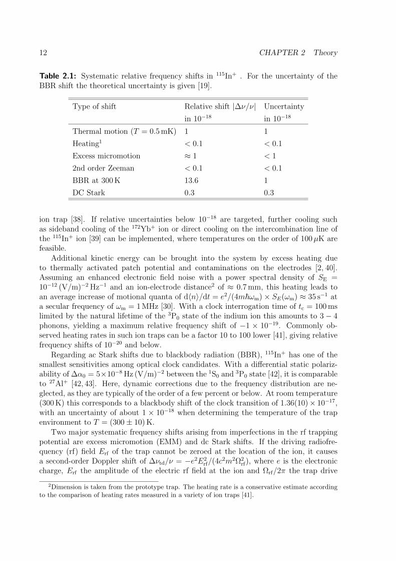
Besides the absence of electronic quadrupole moment, the 1S0 ↔ 3P0 transition in115In+ has the advantage of a very low sensitivity to environmental effects, which aresummarized in Tab. 2.1.
In particular, indium profits from its heavy mass when considering relativistic fre-quency shifts (second-order Doppler shift) due to time dilation ∆νtd/ν = −Ekin/(mc
2),where Ekin is the kinetic energy of the ion, m its rest mass, c the speed of light and νthe frequency of the atomic transition. At the Doppler cooling limit TD = 0.5 mK of172Yb+ this frequency shift amounts to ∆νtd/ν = −Ekin/(mc
2) ≈ −1 × 10⁻¹⁸, whereEkin = 5/2 kBT is the kinetic energy due to thermal secular and micromotion in a linear
1A heating rate of 50 phonons per second at ωm = 2π × 1 MHz is assumed, see text.
12 CHAPTER 2 Theory
Table 2.1: Systematic relative frequency shifts in 115In+ . For the uncertainty of theBBR shift the theoretical uncertainty is given [19].
Type of shift Relative shift |∆ν/ν| Uncertainty
in 10−18 in 10−18
Thermal motion (T = 0.5 mK) 1 1
Heating1 < 0.1 < 0.1
Excess micromotion ≈ 1 < 1
2nd order Zeeman < 0.1 < 0.1
BBR at 300 K 13.6 1
DC Stark 0.3 0.3
ion trap [38]. If relative uncertainties below 10−18 are targeted, further cooling suchas sideband cooling of the 172Yb+ ion or direct cooling on the intercombination line ofthe 115In+ ion [39] can be implemented, where temperatures on the order of 100µK arefeasible.
Additional kinetic energy can be brought into the system by excess heating dueto thermally activated patch potential and contaminations on the electrodes [2, 40].Assuming an enhanced electronic field noise with a power spectral density of SE =10−12 (V/m)−2 Hz−1 and an ion-electrode distance2 of ≈ 0.7 mm, this heating leads toan average increase of motional quanta of d〈n〉/dt = e2/(4m~ωm)× SE(ωm) ≈ 35 s−1 ata secular frequency of ωm = 1 MHz [30]. With a clock interrogation time of tc = 100 mslimited by the natural lifetime of the 3P0 state of the indium ion this amounts to 3− 4phonons, yielding a maximum relative frequency shift of −1 × 10⁻¹⁹. Commonly ob-served heating rates in such ion traps can be a factor 10 to 100 lower [41], giving relativefrequency shifts of 10−20 and below.
Regarding ac Stark shifts due to blackbody radiation (BBR), 115In+ has one of thesmallest sensitivities among optical clock candidates. With a differential static polariz-ability of ∆α0 = 5×10⁻⁸ Hz (V/m)−2 between the 1S0 and 3P0 state [42], it is comparableto 27Al+ [42, 43]. Here, dynamic corrections due to the frequency distribution are ne-glected, as they are typically of the order of a few percent or below. At room temperature(300 K) this corresponds to a blackbody shift of the clock transition of 1.36(10)× 10−17,with an uncertainty of about 1 × 10⁻¹⁸ when determining the temperature of the trapenvironment to T = (300± 10) K.
Two major systematic frequency shifts arising from imperfections in the rf trappingpotential are excess micromotion (EMM) and dc Stark shifts. If the driving radiofre-quency (rf) field Erf of the trap cannot be zeroed at the location of the ion, it causesa second-order Doppler shift of ∆νtd/ν = −e2E2
rf/(4c2m2Ω2
rf), where e is the electroniccharge, Erf the amplitude of the electric rf field at the ion and Ωrf/2π the trap drive
2Dimension is taken from the prototype trap. The heating rate is a conservative estimate accordingto the comparison of heating rates measured in a variety of ion traps [41].

2.2 Theory of Paul traps 13
frequency [38]. This effect is the dominating uncertainty in today’s best ion clocks andaggravates for a larger number of ions. In order to overcome this limitation the trap de-sign presented in this work is optimized to have the maximum possible trapping regionalong the trap axis with an rf field amplitude not larger than 115 V m−1, correspondingto a relative frequency shift of 1×10⁻¹⁸ for a trapped 115In+ ion at a trap drive frequencyof Ωrf = 2π × 25 MHz. In addition, any residual electric field seen by the ion, will giverise to a dc Stark shift νS in the clock transition. Here, 115In+ profits from its low staticdifferential polarizability ∆α0 [42]. At an rf field amplitude of 115 V m−1 this Stark shiftcorresponds to νS = ∆α0 〈E2
rf〉 ≈ 3× 10⁻¹⁹ × ν.Last, the influence of static and dynamic magnetic fields in the ion trap are con-
sidered. The linear Zeeman shift from the mF = 9/2 to mF = 7/2 states amounts to6.36 kHz mT−1 [44] and is due to hyperfine mixing of 3P0 and 1P1 states (the nuclear spinof 115In is I = 9/2). It can be measured and subtracted by alternatively pumping theion into the stretched states of the ground state with opposite magnetic moments [2,45].The second-order Zeeman shift is given by ∆ν = β 〈B2〉. Here, for the alkaline-earthlike system β = 2µ2
B/(3h2∆FS) = 4.1 Hz mT−2, where µB is the Bohr magneton and h
the Planck constant. Owing to the large fine-structure splitting ∆FS = 3.2× 10¹³ Hz ofthe excited triplet states, indium has an advantageously low second-order B-field depen-dency, 10000 times lower than 171Yb+ and 20 times lower than 27Al+. Due to unbalancedcurrents in ion traps, alternating magnetic fields with B2
rms = 2.2 × 10⁻¹¹ T2 have beenobserved [16]. For 27Al+ this leads to an ac Zeeman shift of ∆ν/ν = 1.4× 10⁻¹⁸. How-ever, for the 115In+ ion with ∆ν/ν = 7 × 10⁻²⁰ this effect is negligible at the level of10−18.
While static and dynamic B-fields can be determined quite accurately and frequencyshifts can be taken into account, for an optical clock based on many ions, requirementson the homogeneity of magnetic fields become important. With the given linear Zeemanshift, variations in the magnetic field amplitude should be less than 16 nT across the ionchain to ensure that the broadening of the atomic line is less than 0.1 Hz. Distortionsof the line profile due to spatially varying systematic shifts will have to be evaluatedcarefully to avoid locking offsets. The fast interrogation cycle, that is possible with amulti-ion frequency standard, will be most advantageous when both stretched states areprobed, in order to avoid offsets due to temporally varying magnetic fields.
The above considerations show that it should be possible to evaluate the clock fre-quency of a larger sample of 115In+ ions with a fractional frequency uncertainty of 10−18,assuming that a sufficiently ideal trap can be machined. This issue will be addressed inmore detail in the following sections of this Chapter.
2.2 Theory of Paul traps
2.2.1 The ideal quadrupole trap
A comprehensive insight in the theoretical framework for the trapping of charged particlescan be found in numerous sources in literature [46, 47]. Here, only the basic principlesare illustrated to introduce the relevant equations and parameter.

14 CHAPTER 2 Theory
In one or two dimensions a charged particle can be trapped simply by a static electricpotential. In all three dimensions this is not possible according to Earnshaws theorem.For a potential of the form: ϕ(~x) = Ax2 + By2 + Cz2, with the constants A,B,C ∈ Rthe Laplace equation ∆ϕ = 0 can only be satisfied, if A+B + C = 0.
zz
2z0
y0V
U cos( t)rf rfW Uax
yx
r0
x
Figure 2.2: Schematic of a linear Paul trap with elongated hyperbolic shaped electrodesfor confinement in the radial (xy) plane with an rf potential. Additional ring shapedelectrodes provide confinement in axial direction (along z axis) with a dc potential.
By introducing an oscillating potential, three dimensional confinement can be pro-vided. Consider an ion of mass m and charge e the in a linear trap geometry with radialsymmetry as shown in Fig. 2.2 with an applied potential of the form:
φ(x, y, z, t) =Urf
2r20
cos(Ωrft)(x2 − y2
)︸ ︷︷ ︸+
Uax
z20κ
[z2 − 1
2(x2 + y2)
]︸ ︷︷ ︸ . (2.1)
φrf φax
Here, 2r0 is the distance between opposite radial electrodes, 2z0 the distance betweenthe two ring electrodes and κ a geometrical factor. For the ion the equations of motionread:
d2ri(t)
dt2= − e
m
∂φ
∂ri
, with ri ∈ x, y, z (2.2)
In order to simplify calculations dimensionless parameters are introduced, yieldingthe equations of motion in the form of Mathieu equations:
d2ri
dτ 2+ [ai + 2qi cos(2τ)]ri = 0, with (2.3)
1
2az = −ax = −ay =
4eUax
mΩ2rfr
20
, (2.4)
qx = −qy =2eUrf
mΩ2rfr
20
, qz = 0 and (2.5)
τ =Ωrft
2. (2.6)

2.2 Theory of Paul traps 15
A stable solution for the equations can be found for |a|, |q| 1 and to first order in q:
ri(t) ∼= r0,i cos(ωit+ ϕi)[1 +
qi
2cos(Ωrft)
]. (2.7)
From this it can be seen that the ion motion consists of an oscillation (secular motion)at frequency ω in a pseudo-harmonic time-independent potential:
Ψ(x, y, z) =m
2(ω2
xx2 + ω2
yy2 + ω2
zz2) with ωi
∼=Ωrf
2
√ai + 0.5q2
i , (2.8)
with a modulation at the rf frequency Ωrf (micromotion).This potential is time independent, because the ion is too heavy to follow the rapidly
varying rf potential. Thus, the ion “feels” a ponderomotive force due to the electricfield gradient pointing towards the center when averaged over time. The ponderomotiveenergy is yielded by only looking on the time dependent part of the potential φrf andintegrating Eq. 2.2 over time:
dri(t)
dt=
e
m
∫Erf(ri, t) dt with Erf(ri, t) = −∂φrf
∂ri
, (2.9)
dri(t)
dt=
eErf(ri)
mΩrf
sin(Ωrft) with Erf(ri) =Urf
r20
ri. (2.10)
Averaging over an oscillation period Trf = 2π/Ωrf then yields the ponderomotive energyφpond:
m〈r2i 〉
2=
e2|Erf(ri)|2
4mΩ2rf
= φpond. (2.11)
2.2.2 Excess micromotion
In a perfect trap, without external fields the ion is in average in the center of the pon-deromotive potential at the node of the rf field. With the secular motion reduced byDoppler cooling the motional amplitude of the ion is approximated with the wavepacketextension of a harmonic oscillator in the ponderomotive potential and with ion mass m,which is usually on the order of tens of nanometer. With the rf electric field experiencedby the ion the micromotion is negligible compared to the residual secular motion.
In the experiment, however, strayfields can have dramatic effects on the ion motion.A dc electric strayfield shifts the average position of the ion in the trap by rs,i:
rs,i =e ~Esri
mω2i
, ri =ri
|ri|. (2.12)
The equations of motion now read:
d2ri
dτ 2+ [ai + 2qi cos(2τ)] ri =
e ~Esri
mω2i
, (2.13)

16 CHAPTER 2 Theory
yielding the modified solution:
ri(t) = [rs,i + r0,i cos(ωit+ ϕi)][1 +
qi
2cos(Ωrft)
]. (2.14)
Here, the amplitude of the micromotion rmm,i is directly proportional to the strayfieldand can grow significantly:
rmm,i =1
2rs,i qi. (2.15)
2.2.3 Real traps
For practical reasons, such as access to the ion with lasers or efficient collection offluorescence for detection, the electrodes of an ion trap usually do not have the idealhyperbolic shape. For example, simply four rods with a circular cross section are usedor four blades facing each other [21, 38]. Nevertheless, the equations of motion canbe derived in the same way as for an ideal geometry, except for a modification of thetrapping potential, which will be derived in the following section.
To analyze the shape of the rf potential it is sufficient to consider the spatial partφrf(x, y). In the center of a trap the potential usually can be well approximated with aquadrupole. However, when analyzing the potential in more detail, it is helpful to de-compose it as a series expansion of harmonic functions. Considering the axial symmetryof a linear trap geometry, as shown in Fig. 3.2, cylindrical harmonics as used in Madsenet al. [21] are the functions of choice, yielding the expression for the radial potential incylindrical coordinates:
φrf(ρ, θ) =Urf
2
[∞∑m=0
cm
(ρ
r0
)mcos(m(θ − θ0))
+∞∑n=0
sn
(ρ
r0
)nsin(n(θ − θ0))
],
(2.16)
Here, cn and sn are the expansion coefficients and θ0 is an offset accounting for theorientation of the trap electrodes in the used coordinate system. In Fig. 2.2 θ0 = 0 withrespect to the x axis.
With the coefficient c2, which characterizes the quadrupole term of the potential,the voltage loss factor L ≡ c−1
2 is introduced [48]. It tells how much the voltage has tobe increased for the analyzed trap compared to an ideal quadrupole in order to obtainthe same secular frequency (L = 1 for an ideal quadrupole trap). Using this loss factorand assuming small motional amplitudes the Mathieu equations can be rewritten fornon-ideal trap geometries:
d2ri
dτ 2+ [ai + 2qi cos(2τ)] ri = 0 with ai =
ai
L, qi =
qi
L. (2.17)
The trapping of ions in a Paul trap is based on dynamic confinement, which dependson the Mathieu parameters. When choosing the right values the ion will stay in principle

2.3 Influence of Trap geometry on clock spectroscopy 17
infinitely long in the trap. However, higher harmonic terms of the potential lead toinstabilities of the ion motion in regions, that are otherwise stable in an ideal trap [46].This is important in particular for efficient loading of ions, since ionized particles moveinitially on large radii in the trap before they are cooled.
2.3 Influence of Trap geometry on clock spectroscopy
2.3.1 Trap dimensions and heating rates
During interrogation of the atomic transition in a clock measurement, usually the coolingand repump lasers are switched off in order to avoid light shifts of the measured transitionfrequency. Thus, the trap design has to minimize heating rates of the ions. A typicalsource of heating is thermal electronic noise in the trap electrodes and the trap driveelectronics, which scales with the temperature of the experimental apparatus Ta andthe distance r0 from the ions to the electrodes. The heating rate ˙n then scales as:˙n ∝ Ta r
−20 [30]. Another source of ion heating, that has been observed but not entirely
explained, scales as ˙n ∝ r−40 [30, 31]. Possible reasons for this “anomalous heating”
are fluctuating patch potentials in the electrode material, coated spots from the atomicoven or charges migrating over the surface. In Daniilidis et al. [31] the measured heatingrates of traps from several experiments with different properties are collected and plottedagainst the ion-electrode distance, supporting the overall heating rate dependence withd−4. Nevertheless, a scatter of the data over up to two orders of magnitude at a fixeddistance points to the complexity of the heating rate of an ion trap.
According to this, general guidelines for the trap design include the use of largedimensions for the electrode to ion distance. In Sec. 2.1 a conservative estimate for theheating rate was made using a comparably large ion-electrode distance of 0.7 mm. Thisdistance was chosen following the trend given in Daniilidis et al. [31] and leads to anegligible systematic shift of the clock transition for the case of a single 115In+ ion.
Another reason to increase the trap size is the accessibility of the trap center for therequired lasers. At the same beam diameter reduced stray light of the detection laserfrom the electrodes improves the signal to noise ratio.
A limitation for increasing the trap dimensions is of technical nature. From Eqs. 2.8and 2.5 the dependency of the radial secular frequency on the trap parameters can beapproximated to ωrad ∝ Urf Ω−1
rf r−20 . Thus, when increasing the ion-electrode distance r0
linearly the rf voltage amplitude has to be increased quadratically in order to maintainthe same secular frequency at the same drive frequency. Simultaneously the powerdissipated in the trap increases quadratically with the voltage and the risk of voltagebreakthroughs between the opposite rf electrodes becomes larger.
The secular frequencies, however, need to be kept at a sufficiently high value in orderto allow for recoil-free spectroscopy, i.e. the Lamb-Dicke parameter3 should be muchsmaller than unity, to prevent systematic shifts due to the first order Doppler effect.
3Defined as: η = kx0, with the wave vector k of the spectroscopy laser and the wavepacket extension
of the ion ground state x0 =√
~2mω , with the secular frequency ω in the direction of k.

18 CHAPTER 2 Theory
When scaling up the ion number, this condition is even harder to fullfill. In order tominimize excess micromotion the ions are trapped in a linear configuration by providingstrong radial confinement compared to the axial confinement. Because the rf voltageis practically limited the number of ions in a linear configuration can only be increasedwhen decreasing the axial secular frequency, which in contrast is limited by the increasingLamb-Dicke parameter.
This leads to the ansatz of using a segmented trap, in which small chains of ions areconfined and controlled in an array of independent trap segments. The smaller crystalsare easier to control, e.g. micromotion compensation and nulling of magnetic fields, andsystematic shifts due to residual stray electric and magnetic fields can be estimated withhigher accuracy. In principle, this geometry is scalable to many segments.
2.3.2 RF voltage configuration
For the application of the rf voltage two configurations are possible. In the symmetriccase the signal is distributed to the electrodes as (+Urf/2,−Urf/2,+Urf/2,−Urf/2). Dueto the symmetry of this configuration, no axial field component is present on the sym-metry axis in the center of the trap. In the asymmetric case the signal is distributed as(Urf , 0, Urf , 0), which leads to a non-vanishing axial field component for several reasons,which will be discussed in detail in the next section.
Nevertheless, the asymmetric configuration can be realized more easily due to thefollowing reason. For micromotion compensation in each segment additional dc voltagesmust be applied to the trap electrodes. Doing this on an electrode that carries severalhundreds of volts rf signal, requires careful impedance matching of each electrode withrespect to one another in order to avoid relative phase shifts, that otherwise can lead tonon-vanishing rf fields in the trapping region. The rf signal is coupled to the electrodes viacapacitors, which require very low tolerances in order to avoid phase mismatch betweenindividual electrodes. At the same time they need to be operable at high voltages, whichis not easy to fullfill4.
Therefore, it is easier to couple the additional dc voltages only to rf grounded elec-trodes, whereas the rf signal is provided by a common rf electrode for all segments toreduce relative phase shifts between individual rf electrodes, see Fig. 2.3. To obtainfull control of the radial ion position additional electrodes are placed on top of the rfgrounded electrodes, which will be explained in detail in Sec. 3.2.
2.3.3 RF phase shifts and residual rf fields
By using two common rf electrodes instead of many segments the relative phase shiftscan be reduced significantly. However, the residual phase shifts in this geometry are esti-mated in the following, according to the dimensions of the prototype trap introduced inCh. 3 and admissible tolerances are given in terms of the resulting second-order Doppler
4For this purpose non-magnetic SMD packages with sub millimeter size and a capacitance in thenanofarad range are required. For such elements the typical tolerances for the available capacitance areon the order of a few percent at voltages of a few hundred volts.

2.3 Influence of Trap geometry on clock spectroscopy 19
shift (to satisfy |∆ν/ν| ≤ 10−18 for 115In+ an rf field amplitude of Erf ≤ 115 V m−1 isallowed).
First, the rf field caused by a phase shift ϕac between the signals of the two rfelectrodes is estimated. Assume the potentials Urf cos(Ωrft+
12ϕac) and Urf cos(Ωrft− 1
2ϕac)
each on one of the rf electrodes. According to [38] the phase shift ϕac introduces an rffield Eac in the trap center:
Eac(x, y, t) =Urfϕac α
2r0
sin Ωrft(x+ y)
2(2.18)
where α is a geometrical correction factor, which allows to compare the field in thetrap with and electric field between two parallel plates held at Urf with distance 2r0/α.From the FEM calculations introduced in the following section, the field E0 in the trapcenter is found to be E0 = Urf α/(2r0) ≈ 850 V m−1 at Urf = 1 V, yielding α ≈ 1.2 forthe prototype geometry. From the condition E0 ϕac < 115 V m−1 a maximum tolerablephase shift of ϕac = 0.6 mrad between the rf electrodes is obtained for Urf = 1500 V whenrestricting the induced fractional frequency shift to 1 × 10⁻¹⁸. This is easily obtainedby using a common rf source for both electrodes and reducing the length difference andthe difference in capacitance and inductance of the wires connecting the electrodes to aminimum.
Second, the relative phase shifts ϕrf,i between the indvidual segments i on a commonrf electrode are estimated using a lumped-circuit model of the trap, see Fig. 2.3b. For the
Wrf,n
Ln
d Urf,0
Cel,nCel,1
Cgnd,nCgnd,1
Rgnd,nRgnd,1
Rrf,nRrf,1 Urf,1 Urf,n
UC,nUC,1
a) b)
Figure 2.3: a) Schematic of the segmented linear Paul trap design. The rf potential isapplied on an electrode rail in order to reduce relative phase shifts between the segments.For symmetry reasons slits are cut into the front edge facing the rf ground electrodes.The dimensions are Wrf,n = 6 mm, Ln = 2.2 mm and d = 1 mm. b) Lumped-circuitmodel of the trap design. Included are capacitors coupling the rf ground signal to theelectrodes from a common rail not shown in a). A detailed schematic of the signalconnection on the prototype is given in Fig. 4.11.
electrodes a surface of thick-film gold as described in Sec. 3.3 is assumed. The dimensionsof the electrodes are given in Fig. 2.3a. Here, Rrf,n is the resistance of the rf electrodeper segment with a length Ln and width Wrf,n:
Rrf,n = RLn
Wrf,n
≈ 8 mΩ. (2.19)
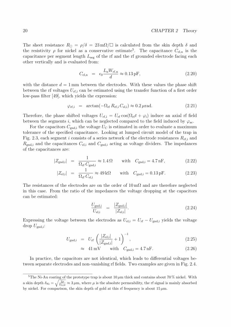
20 CHAPTER 2 Theory
The sheet resistance R = ρ/δ = 23 mΩ/ is calculated from the skin depth δ andthe resistivity ρ for nickel as a conservative estimate5. The capacitance Cel,n is thecapacitance per segment length Lseg of the rf and the rf grounded electrode facing eachother vertically and is evaluated from:
Cel,n = ε0LnWrf,n
d≈ 0.13 pF, (2.20)
with the distance d = 1 mm between the electrodes. With these values the phase shiftbetween the rf voltages Urf,i can be estimated using the transfer function of a first orderlow-pass filter [49], which yields the expression:
ϕrf,i = arctan(−Ωrf Rrf,i Cel,i) ≈ 0.2µrad. (2.21)
Therefore, the phase shifted voltages Urf,i = Urf cos(Ωrft + ϕi) induce an axial rf fieldbetween the segments i, which can be neglected compared to the field induced by ϕac.
For the capacitors Cgnd,i the voltage UC is estimated in order to evaluate a maximumtolerance of the specified capacitance. Looking at lumped circuit model of the trap inFig. 2.3, each segment i consists of a series network of the electrode resistances Rrf,i andRgnd,i and the capacitances Cel,i and Cgnd,i acting as voltage dividers. The impedancesof the capacitances are:
|Zgnd,i| =1
Ωrf Cgnd,i
≈ 1.4 Ω with Cgnd,i = 4.7 nF, (2.22)
|Zel,i| =1
Ωrf Cel,i
≈ 49 kΩ with Cgnd,i = 0.13 pF. (2.23)
The resistances of the electrodes are on the order of 10 mΩ and are therefore neglectedin this case. From the ratio of the impedances the voltage dropping at the capacitorscan be estimated:
Ugnd,i
Uel,i
=|Zgnd,i||Zel,i|
. (2.24)
Expressing the voltage between the electrodes as Uel,i = Urf − Ugnd,i yields the voltagedrop Ugnd,i:
Ugnd,i = Urf
(|Zel,i||Zgnd,i|
+ 1
)−1
, (2.25)
≈ 41 mV with Cgnd,i = 4.7 nF. (2.26)
In practice, the capacitors are not identical, which leads to differential voltages be-tween separate electrodes and non-vanishing rf fields. Two examples are given in Fig. 2.4.
5The Ni-Au coating of the prototype trap is about 10µm thick and contains about 70 % nickel. With
a skin depth δNi =√
2ρΩrfµ
≈ 3µm, where µ is the absolute permeability, the rf signal is mainly absorbed
by nickel. For comparison, the skin depth of gold at this rf frequency is about 15µm.

2.4 FEM calculations 21
UC
U + UC C
D
U + UC C
D
U - UC C
D
Figure 2.4: The same schematic as in Fig. 2.3a. Shown are examples for differentialvoltages ∆UC between the rf ground electrodes due to variations of the capacitors, thatcouple the rf ground signal to the electrodes. These differential voltages induce non-vanishing rf electric fields leading to excess micromotion that cannot be compensated.
For two opposing rf ground electrodes in the same segment i a radial field with anamplitude E
(r)C is induced:
E(r)C,i = E
(r)0 ∆UC,i, (2.27)
with E(r)0 ≈ 850 V m−1 obtained from FEM calculations. A maximum field E
(r)C ≤
115 V m−1 corresponds to a differential voltage drop of ∆UC ≤ 135 mV.In the case of an axial differential voltage as shown in Fig. 2.4 a field with an amplitude
E(z)C is induced:
E(z)C,i = E
(z)0 ∆UC,i, (2.28)
with E(z)0 ≈ 100 V m−1, obtained from FEM calculations. For E
(z)C,i ≤ 115 V m−1 this
yields a differential voltage of ∆UC ≤ 115 mV.Comparing these upper boundaries with the estimated voltage drop Ugnd,i ≈ 41 mV,
it can be seen that for the given value of the capacitance Cgnd,i = 4.7 nF the tolerances forthe capacitors (specified to 10 %) are not critical in order to keep systematic frequencyshifts below 10−18 for the cases described above.
2.4 FEM calculations
2.4.1 Method
Since the trapping voltage is applied in an asymmetric configuration, an axial field com-ponent remains along the trap axis, which leads to micromotion-induced time dilation. Inorder to minimize the axial component and to understand how it is influenced by the trapgeometry a finite element analysis has been carried out. Dimensions of the electrodes,as well as machining tolerances and alignment errors have been investigated [19].
The calculations of the rf field are reduced to an electrostatic problem by consideringthe field at a fixed phase. This is sufficient to determine the field evaluation within the

22 CHAPTER 2 Theory
trap geometry and advantageous to separate these geometrical effects from dynamicalchanges like phase shifts in different regions of the trap as described in the precedingsection. The calculations consist of finding the solution to the electrostatic Dirichletproblem, in which the electrode surfaces of the trap are the boundaries at fixed electricpotentials. For this, commercially available software6 is used. The software provides adiscretization of the space between the electrodes (mesh) and then optimizes a system oflinear equations with between 106 and 8×10⁶ degrees of freedom (mesh points). Furtherdetails on the method and used parameters are provided in [19].
The model used is similar to the one shown in Fig. 2.3a, with the exception that thereis no common rf electrode. Instead, the same electrodes as for the ground potential areused in order to increase the symmetry of the model for a more efficient use of theavailable processor power. The electrodes each have an axial length L = 2 mm, a widthtransverse to the trap axis W = 5 mm and a thickness of 0.2 mm. The overall length ofthe trap, as well as the slit width between the electrodes, are varied for the calculations.
2.4.2 Influence of trap geometry on axial rf field
Two geometrical aspects of the segmented trap design are found to have the highestinfluence on the axial rf field. The first is the finite length of the trap, which leads to anincreasing axial field component along the trap axis with a zero-crossing in the center ofthe trap. For the calculation a single segment with varied length was used in order toisolate the effect of this contribution. In Fig. 2.5 the calculated axial field is shown fordifferent trap lengths at an rf amplitude of 1500 V. Looking at the region in which thefield is smaller than 115 V m−1 corresponding to a fractional frequency shift of ≤ 10−18,the useable region is about half the overall trap length. This is accounted for in the trapdesign by increasing the length of the outer segments, which, because of their differentgeometry, cannot be used for clock spectroscopy anyway. If more trapping segmentsare required, the whole trap length must simply be increased. Due to this behaviour,a limitation is merely present in the overall trap size that can be realized within theexperimental apparatus.
The second feature which leads to axial rf fields is the isolation gaps between theelectrodes. These lead to a dispersion-shaped signal on the trap axis with the magnitudedepending on the gap width, see Fig. 2.6. Here the effect of a single slit between twotrap segments is shown. In order to isolate this contribution, the field obtained due tothe finite trap length is subtracted, here, as well as in the following plots.
With a symmetric configuration for the rf voltage the contribution of each slit atthe same axial position would cancel out. In the asymmetric configuration this happensonly partially even for equal slit widths and perfectly aligned electrodes, so the slits arechosen to be as small as technically feasible.
Having more than two segments, the contributions of each slit add up independentlyand lead to an alternating axial rf field component, as shown in Fig. 2.7. In the centerof each segment where the ions are trapped, the axial field exhibits a zero-crossing, thus
6COMSOL Multiphysics 3.5/3.5a

2.4 FEM calculations 23
-400
-200
0
200
400
-10 -5 0 5 10
Erf(z
) (V
/m)
z coordinate (mm)
Figure 2.5: FEM calculations to evaluate axial rf fields due to the finite length of thetrap. For this a single segment, consisting of four elongated quadrupole electrodes withvarying length was used: 15 mm (red), 20 mm (light blue), 25 mm (green) and 30 mm(violet). For 30 mm length another calculation is made with additional ground electrodesat either end of the trap axis (dark blue). When cutting out the electrode structure ofwafers, the end faces of the gap separating the rf and rf ground electrode arrays aremetallized in order to prevent charge up of insulating surfaces in the line of sight of theions, see Fig. 3.1. The black lines at ±115 V m−1 indicate the amplitude at which rfinduced time dilation is ∆ν/ν = 10−18.
-400
-200
0
200
400
-4 -3 -2 -1 0 1 2 3 4
Erf
,z(z
) (V
/m)
z coordinate (mm)
Figure 2.6: FEM calculations for different widths of the gaps between the trap seg-ments: 50µm (dark blue), 100µm (green), 150µm (light blue), 200µm (red) and 250µm(medium blue). The black lines indicate the region of |∆ν/ν| ≤ 10−18.

24 CHAPTER 2 Theory
providing a region within the trapping area with sufficiently small field amplitudes. Inorder to trap about ten ions in a linear configuration for clock spectroscopy, such a regionis required to be on the order of 100µm.
-1000
-500
0
500
1000
-0.4 -0.2 0 0.2 0.4E
rf,z
(z)
(V/m
)z coordinate (mm)
-1500
-1000
-500
0
500
1000
1500
-4 -3 -2 -1 0 1 2 3 4
Erf
,z(z
) (V
/m)
z coordinate (mm)
a) b)
Figure 2.7: FEM calculations for a three segment trap geometry. The axial positionof the electrodes is indicated by the light blue dashed lines. a) Shown is the axial rffield of two slits, calculated by adding two data sets of a single slit (Fig. 2.6) shifted inz direction with respect to each other. The slit width is varied between 0.1 mm (lightgreen), 0.15 mm (light blue) and 0.2 mm (light red). Adding additional compensationelectrodes on top of the rf ground electrodes in order to enable shifting the ions in theradial plane increases the axial field component (dark blue) by a factor of four for a slitwidth of 0.2 mm. b) Closeup of the plot in a) in the central trapping region. With theadditional compensation electrodes it is possible to trap ions in a region of about 150µm(grey shaded area), where (∆ν/ν) ≤ 1× 10⁻¹⁸.
With laser cutting techniques slits of about 50µm or less can be realized limitedmainly by the ratio of the slit width to the electrode thickness. While for machining theelectrodes are preferred to be thin, the axial rf field component is proportional to theinverse of the thickness. Increasing the thickness by a factor of two reduces the axialfield by about 50 % [19]. Another limitation for increasing the thickness besides themachining is the decreasing detection efficiency due to the decreasing solid angle thatcan be captured by the detection optics.
In Fig. 2.7 the axial field in a three segment trap is shown for different slit widths.The plotted data are obtained by adding the data of two single slits, as shown in Fig. 2.6,between three electrodes of 2 mm length. They are compared with the data of a trapgeometry that contains extra compensation electrodes on top of the rf ground electrodes.Although these additional layers increase the axial field about a factor of four, there isstill a region of about 150µm with low enough time dilation due to the rf field.
2.4.3 Influence of machining and alignment
The requirements of the last sections are based on an ideal geometry without machiningtolerances during fabrication or alignment errors during assembly, which can have signif-

2.4 FEM calculations 25
icant impact on the quality of an assembled trap. Calculations were done to investigatethe influence of these features and the most relevant are presented in the following.
From the machining tolerances a significant influence is due to variations of the slitwidth. In Fig. 2.8 the slit between two electrodes is changed with respect to the otherthree slits, which have all equal and fixed size. Here, the restrictions on the machining
-800
-600
-400
-200
0
200
400
600
800
-4 -2 0 2 4
Erf
,z(z
) (V
/m)
z coordinate (mm)
Figure 2.8: FEM calculations for increasing the width w of a single slit, while theother three slits have a constant width of w = 100µm (dashed green line, taken fromFig. 2.7). The single slit is increased by ∆w = 10µm (dark blue), ∆w = 20µm (green),∆w = 30µm (light blue) and ∆w = 40µm (red). To stay well within the region of|∆ν/ν| ≤ 1× 10⁻¹⁸, the slit width has to be machined with a tolerance of about 5µm.
tolerances for the slits are high. In order to stay well within the field amplitude of115 V m−1, without the extra compensation electrodes, a precision of the machining ofabout 5µm is required, see Fig. 2.8, which cannot be achieved by conventional techniquessuch as milling. Instead laser cutting exhibits more desirable parameters in terms ofprecision. Adding the extra compensation electrodes places a severe limit on the usabletrapping region, which is on the order of 150µm for 200µm wide slits, no machiningtolerances taken into account yet, see Fig. 2.7).
The highest sensitivity to alignment errors during assembly is found for rotationalmisalignment. When rotating two wafers with respect to each other about an axis normalto the wafer plane (x axis in Fig. 3.1) a homogenous axial rf field is found on the trapaxis. This increases with the increasing amount of misalignment. Figure 2.9 shows thefield amplitude calculated for different rotation angles.
At an rf voltage amplitude of 1500 V a maximum rotation of about 0.15 mrad isallowed in order to keep the axial field at 115 V m−1.

26 CHAPTER 2 Theory
-10
-8
-6
-4
-2
0
-4 -2 0 2 4
Erf
,z(z
) (k
V/m
)
z coordinate (mm)
Figure 2.9: FEM calculations for rotational misalignment of the electrode arrays. Therotation angles are 1 mrad (red), 5 mrad (blue) and 10 mrad (green).

Chapter 3
Trap development
This chapter describes the different processes of the trap development from materialconsiderations to the assembly of a fully operational prototype trap.
First, different materials are compared considering mechanical and electric properties.Section 2 details on calculations done with the prototype geometry. The radial poten-
tials due to the rf voltage and the dc voltages for radial asymmetry and axial confinementare analyzed and compared to an ideal quadrupole geometry. Higher order contributionsto the trapping potential are evaluated to avoid dynamic trap instabilities. From thecalculations the Mathieu parameters for all voltages are derived.
Focus of section 3 is the assembly of the prototype trap. The mounting of the electricfilter components on the trap wafers is described, as well as the alignment and glueingprocedure of the trap stack. After assembly the trap is measured again to determinemisalignment during the setup.
In the last section the magnitization of the trap parts is investigated. Single compo-nents as well as the mounted trap stack are characterized in terms of residual magneti-zation.
3.1 Choice of materials – requirements on ion trap
for clock operation
As shown in Ch. 2, a major challenge in the design of a multi-ion trap are residual axialrf fields due to geometrical imperfections or symmetry breaking design. This suggestsa rigid trap design with laser machined electrode arrays, instead of aligning a set ofindividually machined electrodes manually. A way to realize this, is to use electricallyinsulating material as wafers with a metallic coating realizing the electrodes. This ad-ditionally opens the possibility of integrating electronic components such as noise filtersdirectly on the wafers and therefore close to the electrodes.
For this, materials with low dissipative rf losses and high thermal conductivity areconsidered, in order to reduce heating of the trap. Furthermore, the distribution ofdissipated thermal energy becomes more homogenous and allows for a more preciseestimation of the temperature, which reduces the uncertainty of the frequency shift
27

28 CHAPTER 3 Trap development
due to BBR, see Sec. 2.1. Table 3.1 shows a list of possible materials1 and their mostimportant thermal and electric properties.
Table 3.1: Overview of thermal and electric properties of different materials consideredfor machining of the trap boards. The dissipation losses are specified for an rf frequencyof 1 MHz.
Rogers 4350BTM AlN Al2O3 sapphire fused silica
therm. exp. [10−6 K−1] 11...46 3.6...5.6 6.9...8.3 5.9...6.95 0.52
therm. cond. [W m−1 K−1] 0.6 140...180 25 23...25.8 1.38
dielectric const. εr 3.66 8.6 9.9 9.3...11.5 3.8
tan δ [10−4] 31 1...10 5...10 3...8.6 0.15
Compared are aluminum ceramics with fused silica glass, sapphire and Rogers 4350BTM
, a glass-reinforced thermoset laminate which is used for printed circuit boards for high-frequency electronics. All materials exhibit low outgassing rates in ultra-high vacuumenvironment. The ceramics and sapphire exhibit a high thermal conductivity, as wellas comparably low rf losses of tan δ ≤ 10−3. Second, they provide a high mechanicalstiffness, which allows for machining of wafers with thicknesses well below one millimeterwithout losing geometric stability.
However, a challenge is the machining of these materials. Techniques like laser cut-ting provide high precision, but require elaborate development of machining processesthat have to be adjusted carefully to the material in use2. Sapphire is the most chal-lenging material due to its transparency over a large wavelength range and its highrefractive index. This can lead to reflections of the cutting laser inside the material anduncontrollable energy deposition, that prevents from structuring well defined geometries.
Rogers 4350BTM shows the lowest thermal conductivity and rf losses of a few 10−3,which is still sufficiently small in case only low rf power is required for the trap drive. Inshape of thin wafers the material becomes flexible and can reduce the precision to whicha trap is assembled compared to the design. The biggest advantage is, that Rogers iscommercially available including mechanical structuring (milling as well as laser cutting)and metallic coating in flexible layouts.
Based on these informations, machining and coating processes for AlN are developedat PTB. In parallel, a prototype trap is set up from Rogers wafers, that are readily
1Sources of information:Rogers 4350BTM:http://www.rogerscorp.com/documents/726/acm/RO4000-Laminates---Data-sheet.aspx
AlN: http://www.anceram.de/pdf/DBALN.pdfAl2O3: http://www.anceram.de/pdf/DBAL2O3.pdfsapphire and fused silica: http://www.microcertec.com/pdf/Accumet$%$20substrates.pdf.
2For example: Depending on the wavelength and pulse length of the used laser system, parameterslike the scanning speed need to be optimized in order to minimize thermal stress in the wafer, whichleads to cracking of the material. The use of inert process gases has to be optimized.

3.2 Prototype trap design and calculations 29
commercially available to test the trap design and the new experimental setup.
3.2 Prototype trap design and calculations
Based on the FEM calculations from Sec. 2.4 and the material considerations a designfor a prototype trap made of Rogers has been developed with five independent segments,including a separate loading segment and a spectroscopy segment that is free from con-tamination from the atomic oven. A schematic drawing of the geometry is shown infigure 3.1, together with the electronic layout. The rf electrodes Urf only carry the rf
x
y
z z
y
x
Ut - Utc
Ut + Utc
-Uec
+Uec
GNDrf
Urf
Ut,n+
1
Ut,n
Ut,n-1
1m
m
1 mm
0.2
mm
0.2 mm
2 mm
0.2
5 m
m
30 mm
Rogers wafer
Figure 3.1: Trap geometry and electronic configuration. All rf ground electrode seg-ments are dc isolated from each other. With individual voltages Ut,n axial confinementis realized. A differential voltage Utc,n provides compensation fields in radially diagonaldirection in each segment n. A differential voltage Uec,n on the outer compensation elec-trodes provides an independent second field vector to move the ions to any position inthe xy-plane.
voltage for the radial confinement of the ions. The inner rf ground electrodes GNDrf
opposite to the rf electrodes provide dc voltages for the axial confinement as well as formicromotion compensation, while the outer rf ground electrodes are used for micromo-tion compensation only.
For each wafer the ends of the cut out slit are coated and connected to GNDrf , toavoid charging of the surface lying in the line of sight to the trap center.
The prototype geometry is analyzed numerically to derive the relevant trap param-eters. For this, the different voltages are applied to the electrodes and the electrostaticpotentials are calculated using the FEM technique. To obtain the trap parameters ana-lytical expressions derived in Sec. 2.2 are fitted to the numerical data.
The radial rf potential φrf(x, y) is analyzed in detail. First, the electric potential iscalculated fora simplified electrode scheme that consists of four rods with quadratic cross

30 CHAPTER 3 Trap development
section of 200µm size, see Fig. 3.2. In a second step the electric potential is calculatedfor electrodes elongated in one direction to 5 mm to model the electrode shape of theprototype design. Then the extra compensation electrodes are added to model theprototype design. For all calculations Urf = 1 V. In a fourth calculation the prototypedesign is used and the electric potential is calculated for the dc voltage Ut = 1 V that isused to introduce an asymmetry to the radial trap potential.
trap geometry 3
Urf
Urf
0
0
rf trapping voltage
trap geometry 4
Ut
00
0 0
dc voltage forasymmetry
trap geometry 2
Urf
Urf
0
0
trap geometry 1
x
y
Urf
Urf
0
0
Figure 3.2: Trap geometries of which the electric potential is calculated for a voltageUrf = 1 V (left) and Ut = 1 V (right) in order to analyze the influence of the characteristicchanges in the prototype geometry compared to an ideal quadrupole trap. The traplength for all geometries is ltrap = 2 mm. Trap geometry 1: Four rods with squareshaped cross-sections of 0.2 mm size. The distance between the electrodes is 1 mm in bothdimensions. Trap geometry 2: The electrodes are elongated in y direction to a lengthof 5 mm. Trap geometry 3: A pair of compensation electrodes as in the prototypegeometry is added and the voltage is applied asymmetrically. Trap geometry 4: Theprototype geometry is used applying Ut to the inner rf ground electrodes.
The potentials are fitted using Eq. 2.16 for 0 ≤ ρ ≤ 0.7 mm, r0 = 0.707 mm and0 ≤ θ < 360 . The angle θ in Eq. 2.16 is defined with respect to the x axis inFig. 3.2 increasing for counter-clockwise rotation. The offset θ0 added in Eq. 2.16 as afit parameter accounts for the orientation of the potential with respect to the electrodesand defines the principle axes.
From symmetry considerations the number of expansion coefficients can be reducedsignificantly. In [21] it is stated that for geometries such as trap geometries 1 and 2 thepotential is antisymmetric in x = 0 and y = 0 direction3 and symmetric 4 in reflectionsabout the origin and from this, the only non-zero coefficients left are: m = 2, 6, 10, ...and n = 4, 8, 12, ..., see Eq. 2.16. Important to note is, that this is true for a symmetricvoltage configuration (Urf ,−Urf ,Urf ,−Urf). In the case of an asymmetric configuration(Urf ,0,Urf ,0), which is used in this work, additional coefficients contribute, as can be seen
3Translation from r1 = (ρ, θ) to r2 = (ρ,−θ) yields φ(r1) = −φ(r2).4Translation from r1 = (ρ, θ) to r2 = (−ρ, θ) yields φ(r1) = φ(r2).

3.2 Prototype trap design and calculations 31
in Tab. 3.2. Here, the results of the fitting are presented and compared to each other.In all three cases the quadrupole term is the dominant contribution to the rf potential
and the loss factor (Sec. 2.2) of the prototype trap is estimated to L = c−12 ≈ 1.3 for
determination of the Mathieu parameters a and q. The increase of c2 from geometry 1 to2 and 3 is due to the increasing electrodes facing the trap center, hence being effectivelycloser to the ideal hyperbolic shape. Furthermore, the higher order terms converge fasterto zero. For the highly symmetric trap geometry 1 only the cm coefficients give relevantcontributions to the potential, whereas for the geometries 2 and 3 the sn coefficientscontribute as well. The potential at the origin given by c0 is slightly reduced from theideal value Urf/2 in a quadrupole trap due to the reduced screening of the electrodes,which is most apparent for geometry 1 with the smallest electrode surface.
Table 3.2: Overview of fitted coefficients of the multipole expansion for the trap ge-ometries 1 to 4 defined in Fig. 3.2 with Urf = 1 V and U1 = 1 V. The fit errors arewell below the resolution of the last digit for all parameters. Only coefficients with anabsolute value of 0.01 or higher are shown. Due to the strong radial dependence of thehigher order terms reliable values are only obtained when fitting over the full distancer0. The precision of the quadrupole coefficient c2 is not affected by this.
fit parameters trap geometry 1 trap geometry 2 trap geometry 3 trap geometry 4
θ0 −45 −45 −47 50
c0 0.9393 0.9891 0.9577 0.789
c2 0.7279 0.7649 0.7735 0.755
c4 0.0398 – 0.0215 0.092
c6 0.1228 0.0977 0.0862 0.109
c8 – – – 0.026
c10 0.0393 0.0343 0.0273 0.035
c14 0.0132 0.0135 – 0.012
s4 – −0.0282 −0.0263 0.085
s6 – – −0.0337 0.041
s10 – – −0.0194 0.017
Calculations with a symmetric voltage configuration were carried out, to distinguishcontributions to the electric potential from the electrode shape and the voltage config-uration. The c4 term for geometry 1 only contributes in the asymmetric case and isattributed to the finite axial trap length. The calculations show, that the value of c4
grows with decreasing trap length, enhancing the finite length effect.For trap geometry 2 c4 is much smaller (less than 0.01 and not listed in Tab. 3.2).
Another term, s4, contributes more and a comparison between the two voltage configu-rations shows no difference for its value. This suggests, that this term accounts for the

32 CHAPTER 3 Trap development
elongated shape of the electrodes.In geometry 3 more terms contribute due to the more complex electrode structure,
in particular the s6 term accounting for the six electrodes.In Fig. 3.3 the square of the radial electric field, which is proportional to the pon-
deromotive potential, is plotted in the center of the trap.
0
0.1
0.2
0.3
0.4
-3 -2 -1 0 1 2 3
Ele
ctr
ic P
ote
ntia
l (V
)
z coordinate (mm)
2
4
6
8
10
12
14
0 30 60 90 120 150 180
tra
p d
ep
th (
eV
)
q (deg)
b) c)
a)
Figure 3.3: a) Plotted is the squared radial electric field |Erf(ρ, θ)|2 ∝ φpond to indicatethe shape of the ponderomotive potential in the prototype geometry for Urf = 1 V. Inthe center the dominant contribution of the quadrupole term is visible. With largerdistance the higher order term increase and deform the pseudo-potential. Also visible isthe local potential maximum in x direction determining the trap depth, which is plottedin b) as a function of θ. Here, only a region of 180 is plotted, which is sufficient dueto the symmetry. c) Here, the electric potential due to the axial voltage Uax = 1 Vplotted. A fit (light blue) in −250µm ≤ z ≤ 250µm yields the axial confinement to agood approximation. From the potential well the axial trap ϕax depth is etimated.
The rotation of the quadrupole term, see Tab. 3.2 does not affect the ponderomo-tive potential, since this is rotationally symmetric. The higher order terms, however,modulate the ponderomotive potential and lead to resonances that make the ion motion

3.2 Prototype trap design and calculations 33
unstable. The largest contributions to the rf potential are from the c6 and s4 coefficients.Taking into account the radial dependence as well, the contributions of these terms areabout a factor of 1× 10⁻³ or less compared to the quadrupole term5 in a trap region ofabout 35µm for c6 and 120µm for s4.
The modulation of the ponderomotive potential due to higher order contributions isvisualized in Fig. 3.4. Here, the ponderomotive potential is plotted as a function of θ atvarying distance to the trap center. The modulation of about one percent close to thecenter is caused numerically by the interpolation algorithm of the FEM software usedduring data readout. From ρ ∼ 100µm on a modulation with increasing structure andstrength is visible.
0.0353
0.0354
0.0355
0.0356
0 50 100 150 200 250 300 350
fp
on
d(e
V)
q (deg)
0.308
0.31
0.312
0.314
0 50 100 150 200 250 300 350
fp
on
d(e
V)
q (deg)
0.84
0.86
0.88
0.9
0 50 100 150 200 250 300 350
fp
on
d(e
V)
q (deg)
1.5
1.6
1.7
1.8
1.9
0 50 100 150 200 250 300 350
fp
on
d(e
V)
q (deg)
a)
c) d)
b)
Figure 3.4: Ponderomotive potential as a function of θ at various distance to the trapcenter. The values are from a) to d): 50µm, 150µm, 250µm and 350µm.
In practice, the high symmetry of the trap potential has consequences concerningefficient laser cooling. Since, there are no preferred principal axes in which the ionmotion can be decomposed two orthogonal laser beams are required in order to coolall radial degrees of freedom. An alternative is the application of an asymmetry to theradial potential to define principal axes, that allow to use only one cooling laser beamwith projections in both directions.
To introduce a radial asymmetry in the prototype trap the dc voltage Ut is appliedon the inner rf ground electrodes, as indicated in Fig. 3.2. For an asymmetric voltageconfiguration the electric potential has been calculated and fitted at Ut = 1 V, analogueto the rf potential, and the expansion coefficients are presented in Tab. 3.2.
5Calculated is the ratio of the higher order terms to the quadrupole term: φ4
φ2≤ s4(ρ/r0)4
c2(ρ/r0)2 = 10−3 and
φ6
φ2≤ c6(ρ/r0)6
c2(ρ/r0)2 = 10−3. From this the radius is calculated within which the ratio of the contributions is
smaller than the given value.

34 CHAPTER 3 Trap development
Here, the geometry is less symmetric than in the case of the rf voltage, which isclearly visible in the larger number of expansion coefficients. Due to the higher screeningof the electrodes at potential Ut by the extra compensation electrodes on potential zerothe potential of the saddle point is clearly reduced with c0 ≈ 0.79 compared to trapgeometries 1 to 3.
The axis in the direction of the potential maxima is rotated by an angle of θt ≈ 50
with respect to the x axis, from which the principal trap axes 1 and 2 may be definedat angles θ1 = 50 and θ2 = 140 for application of Ut. Due to the asymmetric voltageconfiguration the radial Mathieu parameters due to Ut cannot be calculated with theloss factor. Instead, they can be deduced by directly fitting quadratic functions to thepotential close to the trap center in the direction of the principal axes. Doing so for0 ≤ ρ ≤ 50µm yields curvatures of 8.14 × 10⁵ V m−1 U−1
t and −6.92 × 10⁵ V m−1 U−1t
for 50 and 140 . The fitted curvature as a function of θ is plotted in Fig. 3.5. Thecorresponding Mathieu parameters, which contribute to the radial secular frequencies,are shown in Tab. 3.3.
U = 1Vrf
U = 1Vt
a)
b)
-1.0
-0.5
0.0
0.5
1.0
0 30 60 90 120 150 180
∇2f
t(q)
(10
6V
/m2)
q (deg)
Figure 3.5: Fitted curvature of the electric potential ∇2φt(θ) due to Ut = 1 V as afunction of θ. The principal trap axes are given by the maximum and minimum of thisfunction, which is at about θ1 ≈ 50 and θ2 ≈ 140 . The fitted sine function (red line)indicates the quadrupole shape of the potential.
For a good estimate of the radial secular frequencies, the radial contribution of thepotential φax (see Eq. 2.1), which provides axial confinement in the first place, cannotbe neglected. For this, FEM calculations are done using the prototype geometry withapplication of Uax = 1 V to the rf ground electrodes of the segments adjacent to thecentral segment. A quadratic fit to the data in the direction of the principal axes yieldsthe curvatures −5.58 × 10⁴ V m−1 U−1
ax and −6.28 × 10⁴ V m−1 U−1ax . The corresponding
Mathieu parameters are shown in Tab. 3.3.
With the derived mathieu parameters the radial secular frequencies ωrad,i can be

3.2 Prototype trap design and calculations 35
calculated including all contributions from the rf voltage and dc voltages:
ωrad,i =Ωrf
2
√aax,i(Uax) + at,i(Ut) + 0.5 q2
i (Urf), with i = 1, 2. (3.1)
The axial confinement is given by the potential due to Uax with a fitted curvature of1.192× 105 V m−2 for Uax = 1 V, see Fig. 3.3, which results in an axial trap frequency of58 kHz U
−1/2ax .
The dc voltage Ut, that changes the asymmetry of the radial potential leads to arepulsive potential in axial direction which amounts to a curvature of −1.213×10⁵ V m−2
for Ut = 1 V. The axial secular frequency is then calculated with the correspondingmathieu parameters (see Tab. 3.3):
ωax =Ωrf
2
√aax(Uax) + at(Ut). (3.2)
Looking for the maximum ponderomotive potential as a function of θ the radialtrap depth has been estimated. Figure 3.3a shows the ponderomotive potential with aminimum value in x direction of about 3.3 eV for an rf voltage of Urf = 1 kV.
The axial trap depth is estimated from the potential well introduced by the axialtrap voltage to about 0.35 eV at Uax = 1 V, see Fig. 3.3b.
To summarize the contribution of the rf voltages and dc voltages to the secularfrequencies, the corresponding mathieu parameters are presented in Tab. 3.3, normalizedto applied voltages of 1 V. Here, the parameters are given in the directions x and y aswell, as they are frame of reference for the trap characterization in terms of the rf fieldintroduced in Sec. 5.3.
Table 3.3: List of calculated Mathieu parameters in direction of the radial principalaxes, as well as the geometric axes defined in Fig. 3.1. All parameters are normalized toan applied voltage of 1 V. A comparison with the parameters measured in the prototypetrap is presented in Tabs. 5.1 and 5.2.
axis x y θ1 θ2 z
q 6.69× 10⁻⁵ −6.69× 10⁻⁵ 6.68× 10⁻⁵ −6.69× 10⁻⁵ ≈ 10−3 qrad
at −1.76× 10⁻⁵ 3.82× 10⁻⁵ 1.41× 10⁻⁴ −1.19× 10⁻⁴ −2.09× 10⁻⁵
aax −1.07× 10⁻⁵ −9.0× 10⁻⁶ −9.64× 10⁻⁶ −1.08× 10⁻⁵ 2.05× 10⁻⁵
Table 3.4 shows the dc voltages that can be applied, together with their resolutionand the corresponding dc electric field calculated at the position of the ion.

36 CHAPTER 3 Trap development
Table 3.4: DC voltages for radial trap asymmetry (Ut) and micromotion compensation(Utc and Uec). The corresponding maximum electric field at the position of the ions andits resolution is given along the specified trap axis.
trap axis ∆Udc Udc,range ∆Edc Edc,range
Utc x 0.6 mV 2.5 V 0.32 V/m 1325 V/m
y 0.40 V/m 1650 V/m
Uec x 2.9 mV ±12 V 0.45 V/m 1860 V/m
y 0.05 V/m 204 V/m
Ut z 2.9 mV ±12 V 0.30 V/m 612 V/m
3.3 Trap fabrication
To test the trap design introduced and optimized in the preceding sections a prototypeis built based on Rogers 4350B wafers. For this, two sets of wafers were machined one bylaser cutting and the other by milling, both with a size of 50 mm×50 mm. The thicknessof the laser cut boards is 200µm and 500µm for the milled boards. The electrode designfor both sets is according to Fig. 3.1 with the exception of the size of the gaps betweenthe electrodes. In the case of the laser cut electrodes the gap size is about 220µm andabout 340µm for the milled wafers.
The electrode surface consists of a 35µm thick copper conductive layer and a thick-film gold layer on top. The gold layer has a thickness between 0.3µm and 3µm and ison top of a 0.7µm to 7µm thick nickel layer used as adhesion promoter.
In Fig. 3.6 a closeup on the electrodes of two trap boards are shown, one of which islaser cut and the other is milled. The segment length, slit width and gap between theelectrode array were measured with a calibrated microscope6. Visible is the differencebetween the two machining techniques. The corners of the milled electrodes are less de-fined and give rise to a higher uncertainty in the slit width, which varies in the measuredsample of about 40µm, compared to a scatter of 20µm for the laser machined sample.Furthermore, the edges are rippled on the front side, possibly leading to distortions ofthe trapping potential. The laser cut structures have a higher precision with a loweruncertainty in the corners. Here a difference in quality is visible between the separatedground electrodes of the front and back side (left and right in Fig. 3.6). Due to thehigher quality of the edges and corners machined by both techniques on the back sideof the wafers, the design is adjusted, such that the back side of the wafers is facing theions.
The trap consists of a stack of four wafers that carry the electrodes and are gluedon a 1.5 mm thick carrier board, which provides mechanical stability and the electricalconnections to the trap, see figure 3.7.
Two identical boards (1), one of which is rotated by 180 around the trap axis relative
6Courtesy: A. Ruhz, Dep. 5, PTB

3.3 Trap fabrication 37
2.0 mm2.0 mm
1.1 mm1.1 mm
0.22...0.23 mm0.22...0.24 mm
1.0 mm1.0 mm
1.9 mm1.9 mm 0.33...0.35 mm0.32...0.36 mm
Figure 3.6: Closeup on the electrode region of the machined Rogers wafers. Top: Atrap board ((1) see Fig. 3.7) with laser cut electrodes on front and back side (from leftto right). Bottom: A trap board with milled electrodes on front and back side (leftto right). The back sides face the ions in the assembled trap stack due to the highermachining quality, indicated by the measured distances.
10mm
a)
(3)
(2)
(2)
(1)
(1)
b)
Figure 3.7: a) Photograph of the assembled trap stack with on-board filter electronics,connector pins for dc voltages on the carrier board and rf feed copper strips. b) Schemeof the trap assembly with two trap (1) and two compensation (2) boards with spacers(dark grey) on the corners to provide optical access for the laser beams.

38 CHAPTER 3 Trap development
to the other, form the quadrupole trap. They are separated by four 1 mm thick spacersplaced in the corners. An additional board (2) is attached on top of each of the trapboards, with spacers of 0.25 mm thickness. With the spacers in the corners there isvarious access for laser beams to the trapping region. The carrier board provides goldpins for the dc voltage connections and a mount for the rf connection. The rf lead is a0.1 mm thick, oxygen-free copper foil cut into 5 mm wide stripes of equal length to avoidphase shifts on the rf electrodes.
To prevent coupling of rf power into the dc voltage sources as well as coupling ofhigh-frequency noise onto the trap electrodes, low-pass filters are soldered directly onthe trap boards close to the electrodes. Resistors7 with R = 300 kΩ and capacitors8
with C = 4.7 nF are connected as a first order low-pass with a cutoff-frequency ofνcutoff = 113 Hz. The dc connections from the individual trap boards to the carrierboards are provided by bonding gold wires.
The assembly of both traps is done in four steps. First, the SMD parts and rf leadsare soldered with vacuum compatible solder9 manually. A solder iron with an SMDsuitable tip10 is used in connection with an infrared heating plate, which is held at atemperature between 150 C and 180 C, to compensate thermal losses of the conductivelayers and the copper foil. The temperature of the iron is limited to 275 C to protect theterminations of the SMD parts. The resistors have shown to be more sensitive than thecapacitors and heating times of several seconds lead to destruction of the terminations.
For the copper foil stripes a bigger tip is used to provide enough heating power at thesoldered spot. The SMD parts need to be fixed with a tweezer when soldered, becausethe surface tension of the liquified solder in connection with the low weight of the partsleads to standing up of the parts when melting the solder. Remaining flux is cleaned,with propanole and acetone.
In the second step, the wafers are aligned and glued together. The alignment of thetrap boards is done under a microscope11, that has two translation stages with a scaleof 1µm and a rotation stage with a scale of 10 ′′, which corresponds to 0.05 mrad. Afteraligning one board with the moving stages to a cross hairs the focus of the image ischanged to the other board and the alignment repeated, with the first board being fixedon the table.
After alignment the wafers are glued together with a vacuum compatible glue12, thatcan be cured either thermally or by UV-light. This has the advantage of glueing thewafers one after another with a UV lamp, instead of having to move the whole stackto bring it from the microscope to the oven and risk misalignment. The glue is appliedwith a thin and elastic copper wire in order to avoid misalignment of the loose wafer,which is additionally fixed by putting some weight on top. Another reason to do this isto avoid creeping of glue between the wafers and therefore causing misalignment. The
7company: Barry industries, part number: RP0402BA-3003 JN-918C = 4.7 nF, company: Novacap, part number: 0402 C472 J500 PH-HB9Kester: 80Sn19Ag1Cu
10iron: Weller, 80 W heating power, tip: chisel with (0.15× 0.4) mm11UWM, company: Leitz. Designed for precise characterization of mechanical parts.12Optocast 3410 Gen2, see http://outgassing.nasa.gov

3.3 Trap fabrication 39
glue is cured with a broadband UV lamp13 with 1 W of optical power held at a distanceof about two centimeters above the glue for 200 s.
Figure 3.8 shows, in which order the trap boards are glued. In the beginning the
Figure 3.8: Scheme of the glueing of the trap stack. Starting from the thick spacersin the middle, first the trap boards are aligned and glued, followed by the thin spacersand the compensation boards. Finally, the stack is glued to the carrierboard. The glueis applied with a thin copper wire with high flexibility in order not to push the wafersafter the alignment procedure.
thick spacers are glued to one trap board and stacked with the other trap board toalign and glue them, as well. After fixing the thin spacers to the trap boards, thecompensation boards are aligned and glue one after another. Finally, the stack is gluedto the carrierboard. To make sure, that all glue is cured to avoid outgassing in thevacuum chamber, the trap is put in an oven and baked at 130 C for half an hour.
After glueing the parts together the complete stack is inspected under the microscopeagain, to look for misalignment during the thermal cure. Looking from the top onto thestack only partly allows evaluation of the wafer positions relative to each other. Inaxial direction the upper compensation board covers the electrodes of the upper trapboards, as well as the lower trap board is covered on both sides by the upper trapand compensation board together. To investigate a rotational misalignment of the trapboards the stack is tilted a bit parallel to the trap axis. Like this the edges of both theupper rf electrodes and the rf ground electrodes below are visible. By aligning the crosshairs to both electrode arrays one after another the rotation is measured to be as big asthe resolution of the rotation stage of 0.05 mrad or below. The relative axial position ofthe trap boards was evaluated by looking at the short edges within the electrode slits.Like this a displacement between the upper and lower trap board of about 20µm wasobserved.
In order to avoid mechanical stress on the wafers the dc connections are provided bybonding thin wires to the carrier board, to which the wires are plugged, that connect thetrap with the dc feedthrough of the vacuum chamber. Gold wires with 30µm diameterare used for ball bonding. Because the height difference of the top compensation board tothe carrier board cannot be taken by the bond device, a lifting platform was constructedto compensate for this. For an optimized bonding result, the trap is mounted on a heatingdevice controlled by the bond machine and heated to 80 C. Since the heat conductivityof Rogers is very low, the heating is inefficient and the wedges do not provide sufficient
13company: Dr. Honle, model: Blue Point. Power: 1.5 W for (290...550) nm.

40 CHAPTER 3 Trap development
connectivity, which is why the bond wires are fixed at the end with a second ball.In the last step gold pins are soldered to the carrier board. Kapton R© wires plugged
to the pins provide connection to the dc voltage feedthrough.
3.4 Magnetization of trap parts
The magnetization has been measured for each of the trap parts separately, as wellas for the assembled trap stack, in order to investigate the magnetic properties of thematerials. For this, the measured sample and the field probe are put in a box made ofµ-metal R© to reduce background fields. The probe is fixed to a bar, that can reproduciblybe translated with a precision of about half a millimeter. The measurement is carriedout by shifting the probe across the sample and to look at different field components,either the probe is rotated on its mount, or the sample is rotated on the table relativeto the mount.
Since the samples have to be exchanged or their position needs to be changed, the boxhas to be opened and closed several times between the measurements. It is observed, thatthis leads to scatter of the measured field. To estimate the repeatibility of the measuredfield, the empty box is repeatedly opened and closed and the field inside the box measuredfor a fixed probe position. For this configuration a repeatibility of the measured fieldof σB = 25 nT is obtained. The probe used is a fluxgate14 with a sensitivity of 10 nT.Another reference measurement has been carried out in order to obtain the magneticfield along the scan axis of the probe without a sample, see Fig. 3.9.
x
y z
x
y z
0.1
0.15
0.2
0.25
0.3
-6 -4 -2 0 2 4 6
Bx,r
ef(z)
(µT
)
trap axis coordinate (cm)
-1
-0.9
-0.8
-0.7
-0.6
-6 -4 -2 0 2 4 6
Bx,r
ef(z)
(µT
)
trap axis coordinate (cm)
Figure 3.9: Reference measurement of B-field in the box without a sample. This back-ground field is subtracted from every measurement with a sample in order to improvethe precision. The errorbars show the resolution of the probe of 10 nT.
The probe is rotated such, that the vertical and the horizontal field component trans-verse to the scan direction can be measured. To measure the second horizontal fieldcomponent, the investigated sample is rotated relative to the probe by 90 around the
14type: MAG02

3.4 Magnetization of trap parts 41
x axis, see Fig. 3.9. The used coordinate system is the same as used for the trap, withthe x axis pointing in the vertical direction in the lab frame.
First, the magnetization of the different parts, of which the trap is built of, wasmeasured. The SMD parts show no measurable effect, as well as surprisingly the trapboards, despite a considerable part of the metal coating consists of nickel. As the boardsstick to a strong permanent magnet while lifting it, so the conclusion of the measurementis, that the magnetization of the Rogers boards is less than 25 nT, most likely negligiblefor clock operation.
The gold pins used as dc connectors show a magnetization of Bx = 1.1µT andBy = 0.5µT for a probe distance to the sample of 2.5 mm and 7 mm respectively.
Based on this result, the magnetization was measured with a complete trap stack tomake a conservative estimate of the field at the trap center. The probe was scannedacross the trap and all three field components have been measured. The probe distanceto the trap was 3.5 mm for the vertical field component and 8 mm for the horizontalcomponents. The results are shown in figure 3.10.
magnetization along detection axis
magnetization along trap axismagnetization along vertical axis
B along detection axis
-6 -4 -2 0 2 4 6z (cm)
-6-4
-20
24
6
y (cm)
-1
0
1
2
Bx(y
,z)
()
µT
-6 -4 -2 0 2 4 6z (cm)
-6-4
-20
24
6
y (cm)
-1
0
1
2
Bz(y
,z)
()
µT
-6 -4 -2 0 2 4 6z (cm)
-6-4
-20
24
6
y (cm)
-1
0
1
2
By(y
,z)
(µT
)
-1
0
1
2
z
y
x
Figure 3.10: Measurement of magnetization of the milled Rogers trap. Shown are thethree components of the B-field measured by scanning the probe above the trap.
Above the trap axis the maximal field is ~B = (0.4, 0.3, 0.5)µT. Since the probe canonly be scanned above the trap, this measurement only can give a rough estimation onthe residual magnetic field in the trap center due to the pins.

Chapter 4
Experimental setup
Within this work, the experimental apparatus was set up, that allows to test differenttrap designs. This chapter details on the individual steps. A schematic overview of thevacuum chamber and the imaging system is given in Fig. 4.1, including the atomic ovensand the ion trap.
First, a short review of the atomic structure of the test system 172Yb+ is given tointroduce the relevant transitions. This is followed by a description of the lasers used todrive transitions for Doppler cooling, spectroscopy and repumping of metastable states,as well as photoionization.
Second, the methods for photoionization of ytterbium and indium, as well as thedesign of the atomic ovens are explained. The performance of the ovens is demonstratedby frequency scans of the ionization lasers over the atomic resonances used for photoion-ization.
The vacuum system containing the ion trap and the ovens is introduced and theelectrical and mechanical components are explained.
The control of the ion trap by rf and dc voltages is the focus of the Sec. 4.5. Thehelical resonator used to provide high voltage at low power is introduced. The systemto control the different dc voltages for axial confinement and micromotion compensationis explained and a scheme for calibrating the voltages is presented.
Finally, the detection scheme providing a combination of high sensitivity to fluores-cence of a single ion with a photomultiplier tube (PMT), as well as a high spatial res-olution for Coulomb crystal characterization by an electron multiplying charge-coupleddevice (EMCCD) camera is explained.
4.1 Laser system
4.1.1 Level scheme of 172Yb+
The advantage of the even isotope 172Yb+, used to characterize the ion trap is the absenceof a hyperfine structure and thus a low number of states that have to be addressed. Anoverview of the relevant energy levels is given in Fig. 4.2.
42

4.1 Laser system 43
θ θ
H1
H2
Z
pumps,gauge
aperture
mirror
50/50 bs
EMCCD
PMT
3D translation
optical axis
z
xy
V
ovens
Yb
In
Figure 4.1: Schematic drawing of the vacuum chamber including the ion trap, atomicovens for ytterbium and indium and the detection optics. The laser beams are indi-cated: Cooling and detection in three dimensions H1,H2 and V, repump lasers along thetrap axis Z and photoionization orthogonal to the atomic beams in V (perpendicular tothe paper plane). An aperture with ≈ 1 mm wide slits protects the trap from atomiccontamination outside of the loading segment. The detection is done either with a pho-tomultiplier tube (PMT) or an electron-multiplying charge-coupled device (EMCCD)camera or in a combination of both devices.

44 CHAPTER 4 Experimental setup
369.5 nm
4 MHz
20 MHz
935.2 nm
638.6 nm
2P1/2
3[3/2]1/2
1[5/2]5/2
2D5/2
2D3/2
2F7/2
2S1/2
Figure 4.2: Partial level-scheme of 172Yb+ with atomic transitions used for Doppler cool-ing and detection at 369 nm and repumping at 935 nm. A second repumper depopulatesthe metastable 2F7/2 state, which can be populated by a combination of non-radiativeand radiative decays due to background gas collisions in the vacuum chamber.
For efficient Doppler cooling the 2S1/2 ↔ 2P1/2 transition with a natural linewidth ofΓ ≈ 2π× 20 MHz [50] at a wavelength of λ ≈ 369.5 nm is used. The saturation intensitys0 is given by
s0 =πhcΓ
3λ3, (4.1)
which results to s0 ≈ 510 W m−2 for the given parameters. Furthermore, this wavelengthis used for detection and photoionization of ytterbium, see Sec. 4.3.
Due to the decay channel from the 2P1/2 state to the long-lived 2D3/2 state with abranching ratio of 0.5 % [50], constant cooling of the ion is only possible by depleting thepopulation of this dark state. Light with a wavelength of 935 nm excites the ion to the3[3/2]1/2 state from where the population decays to the ground state, which closes thecooling cycle. In order to avoid optical pumping in the 2D3/2 state, an external magneticfield of about 200µT is applied. Additionally, the fluorescence is optimized by aligningthe polarization of the repumping light with respect to the quantization axis given bythe magnetic field.
Collisions with the background gas in the vacuum chamber can populate the meta-stable 2F7/2 state by a combination of non-radiative and radiative decays [51]. This statehas an estimated lifetime of several years [18,50], so the ion is lost for the experimentalsequence and the decoupling from the cooling-cycle leads to heating and eventual lossfrom the trap. The state population is depleted with a laser at 639 nm. Also, quenchingof the metastable state population via collisions with heavier background molecules suchas H2O is observed.

4.1 Laser system 45
4.1.2 Lasers
Four different diode lasers are used for photoionization, cooling and detection, and re-pumping of 172Yb
+. Four fibers guide the different lasers to the trap, three of which
carry the UV light for cooling and detection and photoionization and one of which car-ries the red and near infrared (NIR) light for repumping. The setup for all lasers isshown in Fig. 4.3. Included in this setup is the photoionization laser for indium, whichfor completeness is described here. Testing of the indium oven and successful loading of172Yb+ /115In+ Coulomb crystals is demonstrated later in this work.
For Doppler cooling and detection of 172Yb+ an optically amplified and frequency-doubled diode laser system1 (extended cavity diode laser (ECDL)) with a maximumoutput power of P369nm = 55 mW is used. Over time a decrease in UV power of thesystem has been observed, mainly due to aging of the tapered amplifier (TA), whosepower dropped from initially 320 mW to 170 mW within three years. After this time theUV power available after optimization of the incoupling into TA and doubling cavityis about 10 mW. By moving the doubling crystal within the cavity a few percent ofthe power can be recovered, which indicates damage of the anti-reflection coating ofthe endfaces of the crystal over time. However, this power is still enough to performspectroscopy on single ions or Coulomb crystals.
The laser is divided into three beams, all sent to the trap via polarization-maintainingoptical fibers. After the fibers, each beam is collimated and imaged into the trap with awaist of w369nm ≈ 80µm using spherical lenses with an effective focal length of 500 mm.The fiber collimators2 are equipped with achromatic lenses, in order to be able to overlapthe Doppler cooling laser with the photoionization laser in the vertical direction, as wellas with the stable laser at 411 nm. This laser is being set up in parallel to this work andwill be used for precision spectroscopy and sideband cooling.
The power used for Doppler cooling and detection of a single ion is ≈ 3µW, whichgives a saturation parameter of s369nm ≈ 0.6 for each beam. In order to perform spec-troscopy on Coulomb crystals in more than one segment, the beams can be expandedalong the trap axis using additional cylindrical lenses, that act as a telescope togetherwith the spherical lenses in the horizontal direction, see Fig. 4.3.
A second ECDL system3 is used as a repumper in the cooling cycle. It provides anoutput power of about 40 mW at a wavelength of 935.2 nm. This light is guided to theions by a polarization-maintaining single mode fiber and focused with a spherical lensof f = 500 mm into the trap along the trap axis Z, see Fig. 4.1. Like this, about 20 mWare imaged with a waist of w935nm ≈ 125µm in the trap.
For a deterministic clean-out of the 2F7/2 state, a second repump laser, at 638.6 nmis used in the experiment with an output power of P639nm ≈ 10.6 mW. About 5.5 mW ofthis light is overlapped with the 935.2 nm laser beam, having a waist of w639nm ≈ 125µmin the trap.
1Toptica TA SHG pro, with DL pro2Schafter & Kirchhoff: for UV: 60FC-4-M10-01 with anti-reflection coating for 400− 700 nm. for IR:
60FC-4-M12-NIR-10 with anti-reflection coating for 630− 980 nm.3DL 100, Toptica

46 CHAPTER 4 Experimental setup
739nm ECDL+ TA + SHG
Doppler coolingYtterbium
PI - Indium
PI - Ytterbium
l/2 l/2
l/2
l/2
l/2
shutter
sh
utt
er
H2
WM
WM
WM
H1
V
MW
MW
repumper cooling
repumper F-state
Z
FC
l/2
l/2
l/2
PD
shutter
l/2
H1
PD
vacuumchamber
optionalcylindrical
lens
wavemeter
opticalswitch
feedback to laserby PC control
beamdump
PPKTP
f=150mm
f= -50mm
f=75mm
P = 55mW
P = 5.8mW
P = 85mW
P = 10.6mW
P = 40mW
f=75mm
Figure 4.3: Left: Schematic setup of the lasers used for 172Yb+ , including the pho-toionization lasers for ytterbium and indium. The cooling and detection laser is split intothree separate beams that are guided by polarization maintaining fibers to the experi-ment. Additionally, the photoionization beams are overlapped with the vertical coolingbeam. The ionization light for ytterbium is obtained by frequency doubling of light at798 nm in a PPKTP crystal in single pass configuration. The indium photoionizationlaser can also be detuned to the 2S1/2 ↔ 2D5/2 transition of ytterbium in order to pop-ulate the 2F7/2 state for spectroscopy of the 639 nm transition. The two repump lasersare overlapped and coupled into a polarization maintaining fiber. An additional fibercoupling for the 639 nm laser provides connection with a frequency comb (FC) in order toperform absolute frequency measurements. Right, Top: Next to the vacuum chamberall lasers are focused with f = 500 mm lenses. The beam H1 additionally provides apower detector. With a cylindrical lens the beams can be expanded in the horizontal di-rection for spectroscopy of linear Coulomb crystals or in more than one segment. Right,Bottom: All lasers are monitored with a wavemeter. Part of them are stabilized bysoftware lock.

4.1 Laser system 47
The overlapping of the two repump lasers leads to the problem of the single modetransmission of light of the used fiber, since the two wavelengths are about 300 nm apartfrom each other. The single mode cutoff wavelength is chosen to about 890 nm whichmeans, that the repumper for the 2F7/2 state is not guided single mode anymore. Instead,the transverse mode of the laser can take a double peak shape, see Fig. 4.4.
125µm 125µm 125µm
a) b) c)
Figure 4.4: Images of the intensity profiles of the two repump lasers at the focus ofthe imaging lens in the axial beam (Z), which is imaged in the trap. a) Image of thesingle-mode output of the optical fiber for the repump laser at 935 nm. The center of thebeam is marked with a cross-hairs, which is kept at the same position in all pictures forcomparison. b) Image of the repump laser at 639 nm for non-optimized fiber coupling.Almost no intensity of the laser is present in the center of the other repump laser, becausethe laser light is not guided single-mode through the fiber. c) Image of the 639 nm laserafter optimizing the fiber coupling with the intensity maximum showing good overlapwith the other repump laser. Both lasers have a measured radius of about 125µm whenoverlapped.
Shown is the shape of the laser beam and its position relative to the Gaussian modeof the 935 nm repumper. It is recorded with a beam profile camera at the focus ofthe beams, which is imaged to the ion position. After adjusting the 935 nm laser onlylittle intensity of the other repumper will be exposed to the ions because of this modestructure, making this laser inefficient. However, by adjusting the coupling of the 639 nmlaser into the fiber the shape of the output can be adjusted to a Gaussian like shapewith a considerable overlap with the 935 nm laser, see Fig. 4.4. Due to the sensitivity ofthis effect to the shape of the fiber, which can be changed by thermal fluctuations in thelab or moving of the fiber, the coupling needs to be checked weekly in order to maintainoverlap of the two beam profiles.
For photoionization of ytterbium, a frequency-doubled ECDL system is used to reso-nantly excite neutral 172Yb to its 1P1 state. An infrared power of 80 mW is guided singlepass through a Brewster-cut periodically-poled potassium titanyl phosphate (PPKTP)crystal, which generates a power of P399nm ≈ 80µW in the second harmonic wave afteroptimized phase matching. The crystal is heated to a temperature of about 51.4 C,which is provided by a heat resistor. A power of 7µW is sent to the atoms through thesame fiber as the vertical cooling beam with an imaged waist of about 80µm.
A second photoionization laser, resonantly exciting neutral 115In, is installed as well,delivering an output power of about 5.8 mW at a wavelength of about 410.3 nm. Thebeam is overlapped with the ytterbium photoionization laser and sent vertically through

48 CHAPTER 4 Experimental setup
the trap as well. The photoionization schemes and the oven design will be explained indetail in Sec. 4.3
4.2 Laser stabilization
A wavelength meter based on a Fizeau interferometer4 with an 8-channel multi-modefiber switch is used to stabilize all lasers. This is realized by a self-written software lock,that compares the wavemeter readout to a set value and applies corrections as a feedbackto the piezo voltage of the laser system as well as the diode current5. Depending on theexposure time of each channel, the fiber switch allows for a maximal readout rate ofabout 1 ms per channel, therefore giving a maximal bandwith of the lock of 1 kHz, ifonly one channel is used. Because there are always four to five channels in use andsome of them require a higher exposure time due to the lower available laser power, thebandwidth is reduced significantly to values in a range of 10...100 Hz.
This stabilization scheme is sufficient to prevent the lasers from slow drifts and is onlylimited by the instability of the wavemeter. The latter was investigated by measuringthe wavelength of a stable laser with the wavemeter and calculating the Allan deviation.The laser used is a diode laser system stabilized to an ULE cavity, which leads to asub-hertz linewidth and a linear drift of ∼ 100 mHz s−1, which can be neglected on timescales of several days. Figure 4.5a shows the Allan deviation of a measurement over 20minutes exhibiting a drift of the wavemeter of about 3 MHz per hour.
-200
-150
-100
-50
0
01 Jul2010
01 Jul2011
01 Jan2011
01 Jan2012
∆n
PI(M
Hz)
0.1
1
10
0.1 1 10 100 1000
Alla
n d
evia
tio
n (
MH
z)
time (s)
a) b)
Figure 4.5: a) Allan deviation of the wavemeter readout from the stable laser at 822 nmover a measuring time of 20 minutes. A drift of ∼ 3 MHz h−1 is deduced. b) The atomicresonance of ytterbium measured over more than one year. The frequency of the 798 nmlaser is given as the difference of the measured resonance to the set value of the laserstabilization. The overall drift is in agreement with the specified absolute accuracy of200 MHz of the wavemeter. A change from day to day of about up to 50 MHz is inaccordance with the drift derived from the measurement of the stable laser.
4High Finesse, WS-75Simultaneous modulation of piezo voltage and diode current is provided by the feedforward function
of the Toptica control unit.

4.2 Laser stabilization 49
On the timescale of seconds the stability is about 1 MHz, which is sufficient to preventthe lasers from drifting within typical measurement time scales of seconds to minutes.For example, during photon-correlation spectroscopy the acquisition time of a singlemeasurement event is 30 s, see Sec. 5.2.
To evaluate the instability on longer time scales a measurement of the atomic reso-nance at 399 nm as a function of time is plotted over a period of more than one year, seeFig. 4.5b. The measured deviation is in agreement with the specified abolute accuracyof 200 MHz in multi-channel switch operation. A day to day drift of about 50 MHz isconsistent with the drift estimated from the Allan deviation.
Recording the wavelength of this laser over several days together with the ambienttemperature of the wavemeter reveals a clear dependence of the wavemeter readout withthe temperature, with a proportionality factor of 15 MHz K−1.
In order to correct this drift on the different laser wavelengths, the atomic resonancesand the resonance of the cooling transition have been measured repeatedly and comparedto the frequency of the stable laser. Figure 4.6 shows the correlation of the different lasers,giving a linear function with characteristic slope for each laser l: ν(l)(t) = s(l) · ν822(t).With this correlation it is now possible to correct the set values for the individual lasersν
(l)set by monitoring the drift of the wavemeter output of the stable laser ν822(t+ ∆t) after
time ∆t. Multiplying the drift with the individual slope a correction can be applied tothe set value for the lock of each laser in order to compensate for the wavemeter drift:ν
(l)set(t+ ∆t) = s(l) · ν822(t+ ∆t).
-90
-60
-30
0
30
500 520 540 560 580
∆7
39
(MH
z)
∆822 (MHz)
-210
-195
-180
-165
-150
480 490 500 510 520
∆7
98
(MH
z)
∆822 (MHz)
-60
-30
0
30
480 490 500 510
∆4
10
(MH
z)
∆822 (MHz)
a) b) c)
Figure 4.6: Correlation of measured frequency of the stable laser ∆(822) = ν(822) −364 738 000 MHz with the wavelength of the other lasers, in order to compensate waveme-ter drifts based on the stable laser as a reference. For each laser l a linear functionν(l)(t) = s(l) · ν822(t) is fitted in order to correct the set values of the laser stabilizationafter a drift of the wavemeter measured with the stable laser. The frequencies plottedare relative to the according set values: ∆(l) = ν(l) − ν
(l)set. The set values and fitted
slopes are a) ν(739)set = 405 646 363 MHz, s(739) = 1.36± 0.09, b) ν
(798)set = 375 763 584 MHz,
s(798) = 0.93± 0.08 and c) ν(410)set = 730 692 762 MHz, s(410) = 1.9± 0.7.
Worthwhile mentioning is the fact, that the repeatibility of the wavemeter decreases inthe range of short wavelengths, which can be seen in the higher scatter of the measuredneutral indium resonance compared to the ytterbium resonances. For ytterbium allmonitored wavelengths are in the red and near infrared (NIR) range.

50 CHAPTER 4 Experimental setup
4.3 Atomic oven design and photoionization of Yb
and In
In the experiment 172Yb+ and 115In+ ions are created by photoionization of atoms in thetrapping region.
Both ionization schemes consist of a two-step excitation, in which the atoms are firstexcited resonantly to an intermediate state with the photoionization lasers described inSec. 4.1. To reach the ionization threshold in the case of ytterbium the energy of twophotons at 399 nm is not sufficient. For this the cooling laser is used. In the case ofindium the ionization threshold is lower than the energy of two photons at 410 nm, thusone laser is sufficient. Both schemes are visualized in Fig. 4.7 and Fig. 4.8.
The oven design consists of a vertical tantalum tube with an outer diameter of1.02 mm and an inner diameter of 0.86 mm. On both ends, copper wires are spot-weldedto provide the heating current, see Fig. 4.7. A 0.4 mm diameter hole on the side of thetantalum tube generates a cone of atomic vapour. To collimate the atomic beams ofboth ovens, a copper shield with two slits of ≈ 1 mm in the horizontal direction is placedbetween the ovens and the trap, assuring atomic flux through the loading segment, whilethe spectroscopy segments do not get contaminated, see Fig. 4.1.
Because the collimated atomic beams pass horizontally through the trap and thephotoionization light is guided vertically, Doppler shifts and broadening of the atomiclines are avoided.
For ytterbium an isotopically-enriched sample is used, as the natural abundance ofthe isotopes 172Yb and 173Yb are 22 % and 16 %, respectively. Their photoionizationresonances are separated by only 55 MHz and exhibit considerable overlap, which is whyit is important to avoid broadening effects. Two frequency scans of the photoionizationlaser are shown in Fig. 4.7. The earlier one displays the dominant peak for the isotope172Yb, but also a residual abundance of other isotopes, in particular 173Yb. The full-width half maximum is measured as about 35 MHz at a saturation parameter of s =2Ω2/Γ2 . 1, where Ω is the Rabi-frequency and Γ the decay rate of the excited state.Within about four months a depletion of the other isotopes occured without recoveringagain, which is shown in the later scan.
Furthermore, an image of the loading segment is shown in Fig. 4.7. Neutral ytterbiumatoms are visible in the trace of the photoionization laser passing vertically through thetrap. The bright spot in the middle of the trapping region is a cloud of laser cooled172Yb+ ions. The collimation of the atomic beam could be verified by scanning thelaser beam through all trapping segments and detecting fluorescence only in the loadingsegment. A beam width of about less than two millimeters was observed positioned inthe center of the loading segment.
The indium oven has been tested as well. Because the natural abundance of 115In isabout 95 % an enriched sample is not necessary. As a source a piece of a wire of 99.999 %pure indium that fits in the tube is used. In the case of indium the only material suitablefor the oven is tantalum, since it is the only metal that does not alloy with indium.
By detecting an atomic signal with the same beam alignment as for the ytterbium

4.3 Atomic oven design and photoionization of Yb and In 51
0
2000
4000
6000
8000
10000
-1200 -1000 -800 -600 -400 -200 0 200 400 600
sig
nal (a
.u.)
D (MHz)
176Yb
173Yb(5/2)
174Yb
173Yb(3/2)
172Yb
173Yb(7/2)
171Yb(3/2)
171Yb(1/2)
scan from 28.02.2011
scan from 26.10.2010
29 MHz
398.9 nm
369.5 nm
ionization
1P1
1S0
Figure 4.7: Left: The ionization scheme for ytterbium as a two-step excitation. Right:Scan of the 399 nm laser with isotope enriched 172Yb sample. The expected resonances ofthe various isotopes [52] are indicated by triangles. The left inset shows a picture of theloading trap segment with atoms fluorescing in the trace of the vertical photoionizationlaser. The bright spot is a cloud of laser cooled 172Yb+ ions. The right inset shows adrawing of the oven. At the ends of the tantalum tube copper wires are spot-welded,which are separated by a macor spacer held together by a steel ring.

52 CHAPTER 4 Experimental setup
laser, the adjustment of the indium oven to the loading segment was confirmed. InFig. 4.8 a frequency scan of the photoionization laser is shown. The resonances are
-2000
0
2000
4000
6000
8000
10000
12000
-10.1 -1.6 1.4 9.8
sig
nal (a
.u.)
n - 730 683.0 (GHz)
(2)
(1)
(3)
(4)
22 MHz
410.3 nm
410.3 nm
ionization
2P1/2
2S1/2
HFS
(1)(2)(3)(4)
F=5
F´=4
F´=5
F=4
Figure 4.8: Left: The ionization scheme for indium as a two-step excitation with a singlelaser. Because of the hyperfine structure (HFS) four lines are visible in the scan. Right:Scan of the 410 nm over the resonance. The signals are fitted with Lorentzian functiongiving linewidths between 50 MHz and 70 MHz for a saturation of s ≈ 6. The highestrelative intensity of line (3) suggests most efficient ionization with this line. The relativestrengths of the individual lines show good agreement with previous measurements [53].
fitted with a Lorentzian function and the obtained linewidths are between 50 MHz and70 MHz due to a saturation of s ≈ 6. From the relative signal strengths the most efficientionization can be achieved with resonance (3).
4.4 Vacuum system
The vacuum chamber is based on a DN250 tube with flanges on the side to connect var-ious windows. A horizontal cut through the chamber including all relevant componentsof the system is shown in Fig. 4.1. At the bottom flange all electrical feedthroughs anda window for the vertical beam axis (V) are located. An 8 pole high current feedthroughprovides connection with the ovens, a coaxial high voltage6 connector provides the rf feedfor the trap. A 41 multipole connector provides the dc voltages for axial confinementand micromotion compensation.
The windows on the side of the chamber have an anti reflection coating in the ultravi-olet (UV) range with a local minimum at 230 nm for the indium spectroscopy laser. Forthe detection a reentrant window with a non-magnetic seal is mounted with a distance of23 mm to the trap in order to obtain higher collection efficiency of the ion fluorescence.Two horizontal beam axes (H1 and H2) are provided by four windows, aligned under25 to a third axis (Z), which is in the direction of the trap axis.
6HN-type

4.5 Trap drive 53
Opposite to the reentrant window the vacuum pumps and an angle valve for connec-tion of a turbo molecular pump for initial pumping are mounted. After that the vacuumis maintained by an ion getter pump7, having a nominal pumping speed of 20 mbar l s−1
for air and a titanium sublimation pump8 in a DN63 tube, with a calculated pumpingspeed of 490 mbar l s−1 for hydrogen.
After closing the chamber for the first time, a bake out was done with every compo-nent built in except for the ion trap. The temperature was kept between 190...200 C fortwo weeks in order to clean the system and to reduce desorption of hydrogen from thechamber walls. After this, the chamber was reopened to insert the trap contaminatingthe chamber with water vapour from the air. From this conditions a residual pressure of∼ 1.5× 10⁻⁹ mbar was obtained after pumping. Within a few months and by repeatedlyfiring the titanium sublimation pump9 the pressure could be reduced to ∼ 4×10⁻¹⁰ mbar.
With the trap built in a modest bake out was done in order to further reduce thewater in the chamber. For two weeks the temperature was kept between 60...100 Cleading to a reduced pressure of ∼ 1.5× 10⁻¹⁰ mbar.
After changing the laser cut ion trap with the milled trap a third bake out was done.The temperature was kept between 100...125 C for five days resulting in an end pressureof ∼ 8× 10⁻¹¹ mbar.
4.5 Trap drive
4.5.1 RF voltage drive
For the application of the rf voltage to the ion trap a helical resonator is used. Onereason for this is to match the impedances of the amplifier output and the trap in orderto reduce the power necessary for a given voltage. Another reason is the filtering ofamplifier noise by the resonator due to its small bandwidth at a high Q factor.
According to MacAlpine et al. [54] the resonator was designed for an unloaded reso-nance frequency of about 45 MHz. Given the capacitance of the ion trap (see Ch. 2) theresonance frequency of the trap – resonator system is expected to drop to about 25 MHz,the designated trap drive frequency. A schematic of the resonator design is shown inFig. 4.9.
On the incoupling side a single winding coil is mounted next to the resonator coil toinductively transmit the power into the circuit. The coupling is optimized by alteringthe distance between the two coils for impedance matching.
After setting the distance to the optimized point an unloaded Q factor of Qu ≈ 1050was reached. Connecting the resonator to the trap a loaded Q factor of Ql ≈ 640was obtained in the case of the laser cut trap with a resonance frequency of Ωrf =2π × (25.67± 0.01) MHz. For the milled trap, which was built in at a later time, the Qfactor amounts to Ql ≈ 590 at a resonance frequency of Ωrf = 2π × (25.42± 0.01) MHz.
7Varian starcell8Varian TSP filament9For this a current of 47 A is applied for one minute.

54 CHAPTER 4 Experimental setup
soldered
47.5 47.5
11
0
60
ø 1
20
25
9.5
90
185
10
2
inco
up
ling
sid
e
pic
ku
p s
ide
connector tofeedthrough
0
200
400
600
800
1000
25.6 25.65 25.7 25.75
Um
on2
(mV
2)
νrf (MHz)
Figure 4.9: Left: Schematic drawing of the helical resonator for rf voltage generation,the dimensions are given in mm. A pickup not drawn here is mounted on the left cover.The incoupling coil is mounted on the right side. Right: Measurement of the resonancewhen connected to the milled trap. The fitted Lorentzian function has a full width athalf maximum of ∆ν = (39.0± 0.7) kHz and a maximum at ν = 25.67 MHz, which givesa Q factor of Ql = ν/∆ν ≈ 640.
The loss in the Q factor compared to the laser cut trap is possibly due to the thickerwafers of the milled trap, in which more rf power is dissipated.
A schematic of the rf electronics is shown in Fig. 4.10. The rf signal from a frequencygenerator10 is split into two paths one of which is used for the trap drive, whereas theother one is used as a trigger for the photon-correlation spectroscopy, see Sec. 5.2. Amixer11 is used to add modulation signals, e.g. for parametric heating of the ions tomeasure secular frequencies. The modulated signal is amplified12 and coupled into thehelical resonator, which is connected to the trap. The attenuator before the mixerreduces the signal by 3 dB to optimize the working range of the rf generator, in whichno internal switching occurs that otherwise leads to the loss of the ions.
In order to monitor the rf voltage on the trap electrodes a thin copper wire is placedinside the helical resonator sensing a monitor voltage Umon. The monitor voltage iscalibrated by measuring the output voltage of the coil with a low capacitance field probeyielding a calibration factor κ = 5400± 340.
10Marconi: 202411minicircuits: ZAD-6+12minicircuits: ZHL-5W-1, amplification: 46 dB

4.5 Trap drive 55
rf generator
f/2
1
2
S
attenuator
MCB
R L
I
TAC
start stop
out
modulationsignal
pmtsignal
PC
pickup
mixer amplifier helical resonator
Figure 4.10: Schematic of the rf circuit for the trapping rf voltage. The rf signal issplit into two paths, one of which used for photon-correlation measurements (setup inthe green box, a detailed description is given in Sec. 5.2). The other part is amplifiedand coupled to the helical resonator for impedance matching of the amplifier with theresonator. The rf mixer in between can be used to modulate the signal, e.g. for paramet-ric excitation of secular ion motion or as a controlled switch of the trapping potentialamplitude. The rf electrodes are connected directly with the output of the resonatorvia copper foil leads and the coaxial feedthrough. The GNDrf electrodes are connectedwith the vacuum chamber as is the resonator shield. The rf signal coupled inductivelyinto the resonator has an independent ground connection from the resonator. From thepickup the monitor voltage Umon is read out with an oscilloscope.

56 CHAPTER 4 Experimental setup
4.5.2 DC voltages
The dc voltages are generated by an analog output PCI card13 and software controlled.The outputs are connected to a self-built control unit, in which the trapping voltage Ut
and the compensation voltages Utc and Uec are added up and scaled appropriately, whichwill be discussed in the following. The control unit is then connected directly with thefeedthrough of the vacuum chamber by a pairwise shielded multi-core cable in order toreduce coupling of high-frequency noise.
+U
ec
U-
Ut
tc-U
ec
U+
Ut
tc
Ut Utc Uec
U - otc tc
stc
U - ot t
st
U - oec ec
sec
calibration
inputPC control
CR
CR
CR
CR
Urf
Urf
analog outputs
sU + s Ut t tc tc
sU - s Ut t tc tc
+s Uec ec
-s Uec ec
DC control unit
Figure 4.11: Schematic drawing of the dc voltage control. The voltages are generatedwith the AO card and distributed in the DC control unit. On the trap wafers the voltagesare connected to the electrodes in series with a resistor in order to avoid currents backto the control unit. The capacitors connect the electrodes to rf ground, simultaneouslyshorting high-frequency noise to rf ground. The signals are calibrated within the PCcontrol software, but split up and added (subtracted) by independent electric circuitswithin the DC control unit. Due to this, the calibration can be done with a precisiongiven by the tolerances of the electric components in the different circuits.
As shown in Fig. 3.1, Ut is applied to both GNDrf electrodes of a trap segment forproviding axial confinement or squeezing of the radial trapping potential. Utc is addedon one electrode but subtracted on the other in order to create an electric field formicromotion compensation. This is realized in the control unit by two independentelectric circuits, whose outputs are directly connected with one of the electrodes for each
13National Instruments: NI 6723 with 32 analog outputs

4.5 Trap drive 57
trap segment. Another two circuits provide the compensation voltage Uec, one withpositive and the other one with negative sign. A schematic of the dc voltage generationand connection is shown in Fig. 4.11
The circuits provide low pass filtering and scaling of the voltages as well. The compen-sation voltage Utc is divided down by a factor of four in order to improve the resolution.For the extra compensation electrodes Uec is multiplied by 1.2. First, because the dis-tance to the ions is larger and the applied field therefore becomes smaller for the samevoltage and secondly to use the full range of the operational amplifiers used. The analogoutputs of the PCI card have a range of ±10 V and a resolution of 13 bit, yielding a stepsize of 2.44 mV. The obtained resolution for the different dc electric fields is given inTab. 3.4.
The whole system is calibrated by measuring the output voltages for given inputvalues and applying corrections to the input values within the control software. Forthis the output values are plotted against the input values and a linear function Uout =oc + sc · Uin is fitted, Fig. 4.12a shows a measurement of Ut on the GNDrf electrodes ofsegment 2. The obtained calibration parameters oc and sc are applied to the input valuesin the control software: Ucal = (Uin− oc)/sc. As a cross-check Ut is measured again aftercalibration, see Fig. 4.12b.
a) b)
-6
-4
-2
0
2
4
6
-6 -4 -2 0 2 4 6
Uca
l-
Uo
ut(m
V)
Ucal (mV)
-9
-6
-3
0
3
6
9
-6 -4 -2 0 2 4 6
Uo
ut(V
)
Uin (V)
Figure 4.12: Example for the calibration of the dc voltages, shown is a measurement ofUt on both GNDrf electrodes 1 (blue cross) and 2 (red x) of trap segment 2. a) Outputvoltage measured before calibration showing the scale factor of 1.2. A linear function isfitted to obtain the calibration factors: o
(1)c = (−4.5 ± 0.3) mV, s
(1)c = 1.2110 ± 0.0001,
o(2)c = (−3.5 ± 0.3) mV and s
(2)c = 1.2106 ± 0.0001. b) Output voltage measured after
calibration with the applied corrections o(1)c = −4.5 mV, o
(2)c = −3.5 mV and sc =
(s(1)c + s
(2)c )/2 = 1.2108. The residual error due to the two different scalings is ≤ 10−3
for all dc electrodes.
The output voltages for the two electrodes providing Ut + Utc and Ut − Utc are notperfectly balanced, because they are provided by independent circuits, that operate withindependent voltage dividers. The latter are matched only within their specification andcan therefore not deliver equal outputs for a common input signal. The residual errorin the scaling is ≤ 10−3. For the correction the average value of both measured scalefactors is chosen.

58 CHAPTER 4 Experimental setup
The measured offset of a few millivolt stems from the PCI card, whose analog outputshave a specified absolute acurracy of 10.78 mV at full range (±10 V).
4.6 Detection
The detection scheme, as shown in Fig. 4.1, is twofold: it is possible to either detectwith the EMCCD camera14 or with a photomultiplier15. Also, it is possible to detections with both devices simultaneously using a 50/50 beam splitter. Figure 4.13 shows aschematic of the lenses.
6.8 6.83.7 3.74.05
0.54.0 20.75 5.0
1.44
Figure 4.13: Schematic drawing of the self-built retro focus optics for single ion detectionusing five spherical lenses with one inch diameter. The focal lengths are from left toright: 50 mm, 250 mm, 50 mm, −25 mm and 250 mm. The dimensions are given in mm.The optimal distances between the lenses was calculated with commercial ray tracingsoftware. For diffraction limited imaging, tolerances of 0.1 mm to 0.01 mm need to beadhered to.
The optics is a five lens retro focus system optimized with commercial ray tracingsoftware16. The distances of the lenses are optimized for a wavefront error of less thanλ/4. The lens has a working distance of 31 mm and a numerical aperture of NA ≈ 0.27,which allows for a collection efficiency of about 2 % of solid angle. The lenses have abroadband UV anti-reflection coating including the detection light of 115In
+. The optics
is mounted on a three-axis translation stage.
The whole optical path is encapsulated in order to avoid stray light. In the boxcontaining the mirror and beam splitter a filter is protecting camera and photomultipliertransmitting only the wavelength of the detected light. Different filters are exchangedmanually in order to detect the atomic signals of indium and ytterbium or the fluores-cence of ytterbium ions.
14Andor: DU-897, 512 px× 512 px, quantum efficiency QE = 35 % for 200 nm− 370 nm15Hamamatsu: R7207-01, Bialkali window, QE ≥ 20 % for 160 nm− 650 nm16Oslo

4.6 Detection 59
In this setup a magnification of V ≈ 25 is designed, yielding with the pixel sizeof the camera of 16µm a theoretical resolution of about 600 nm. At the wavelengthλYb+ = 370 nm the diffraction limit is estimated to be dxmin = λ/(2NA) ≈ 570 nm. Theresolution achieved in the experiment is about 1.5µm. This was evaluated by measuringthe half width at full maximum of a fluorescence spot of a single ion. An estimation ofthe wavepacket extension xx of the harmonic oscillator at the Doppler limit for 172Yb+
of TD ≈ 0.5 mK yields xD =√
kBTD2mω2
z≈ 175 nm, with an axial secular frequency of
ωz = 2π × 100 kHz.

Chapter 5
Characterization of prototype trap
In this chapter measurements are shown to characterize the prototype trap and comparethe experimental results with the calculations presented in Ch. 2 and 3.
First, the controlled loading of 172Yb+ ions into the laser cut trap is demonstratedand the optimized parameters for a controlled loading process are presented. Further-more, the capability of trapping and Doppler cooling Coulomb crystals is demonstrated.Secondly, the secular frequencies of a single ion are measured in both traps by para-metric excitation of the ion motion and the Mathieu parameters are derived. These arecompared to the estimated values presented in Sec. 3.2.
Residual rf electric fields are measured in both traps using photon-correlation spec-troscopy. The method is explained in detail, as well as the evaluation of rf electric fieldsfrom the obtained data. Particular effort is put into the quantitative analysis of the dataand the determination of the sensitivity of the spectroscopy method.
With this, excess micromotion is measured in all dimensions in the trap and com-pared to the FEM calculations presented in Sec. 2.4 and 3.2. The radial electric fieldcomponents are used to calibrate the spectroscopy, because the numerical estimationgives reliable results within a few percents. The axial field component, which is aboutthree orders of magnitude smaller than the radial component, is also measured andcompared to the calculations. From this measurement, a deviation from an idealizedgeometry to the built prototype trap can be estimated. For the axial rf field both thelaser cut trap and the milled trap have been investigated and compared with each other.
Using the photon-correlation spectroscopy, other properties of the laser cut trapare characterized. By compensating the micromotion in the loading segment as wellas in the adjacent central segment over several loading cycles, the influence of atomiccontamination from the oven is investigated. Longterm measurements on different timescales demonstrate the stability of micromotion compensation, a particular requirementfor ion traps in a clock. The crosstalk of the compensation voltages to neighbouring trapsegments has been measured and compared with the theoretical values.
60

5.1 Loading and trapping ions 61
5.1 Loading and trapping ions
5.1.1 Deterministic loading of 172Yb+ ions
For a first test to trap ions, a single lens was used to observe the whole trapping re-gion. The photoionization laser was sent through the trap vertically and aligned alongthe trap axis until fluorescence of neutral ytterbium was observed while scanning thelaser frequency. Both lasers were scanned in frequency over the estimated resonancesuntil fluorescence was observed, after which the parameters could be optimized and theresonances could be measured.
To test functionality of all trap electrodes, ions were loaded and shuttled into allsegments. Figure 5.1 shows two ion clouds trapped simultaneously and each illuminatedby one of the horizontal beams H1 and H2.
20µm
1 2 3
Figure 5.1: Top: Trapping of clouds of 172Yb+ ions in segments 1 and 3, illuminated bybeams of the cooling laser along H1 and H2. The stray light of the laser beams makesthe segmented trap structure visible. Bottom: Picture of a linear Coulomb crystal of37 172Yb+ ions, trapped in segment 3 and imaged with the self-built lens.
The detection lens described in Sec. 4.6 was initially aligned by imaging the straylight of a laser pointer with a wavelength of 410 nm and power of 1 mW illuminatingthe trap electrodes. The position of the lens when imaging the corners of the electrodeswas recorded to interpolate the lens positions for the trapping region. For positioningalong the optical axis, a correction due to chromatic aberration was applied taking intoaccount the different wavelengths of the laser pointer and the cooling laser.
The conditions for controlled loading of single ions were investigated by varying thepower of the photoionization laser as well as the oven current. The optimal compromisefor both parameters was found by looking at the probability to generate reliably notmore than a single ion within a loading period of about one second or longer. Theoptimal parameters found are about P399 ≈ 5µW and Ioven ≈ 5.5 A. In Fig. 5.2 thefluorescence of ions loaded with a continuously running photoionization laser is shown.Visible are the typical steps of the signal as each new ion appears and the Coulombcrystal is rearranged. Also visible is the drop in fluorescence at the time of ionizationdue to the heating of the crystal by the initially “hot” new ion.

62 CHAPTER 5 Characterization of prototype trap
single ions
0
50
100
150
200
250
300
0 20 40 60 80 100 120
ion
flu
ore
sce
nce
(kcp
s)
time (s)
a) b)
0
20
40
60
80
100
120
0 2 4 6 8 10
3
4
5
6
7
8
Yb
sig
na
l (k
cp
s)
I ove
n(A
)
time (min)
Figure 5.2: a) Loading of ions into the laser cut trap, with the arrival of each newion indicated by a step-like increase of the fluorescence. The drop of fluorescence atsome of the steps is caused by heating and temporary melting of the crystal when a newion arrives with high kinetic energy. b) Fluorescence of neutral ytterbium for differentoven currents. The blue (green) curve is recorded with a starting current of Ioven = 6 A(Ioven = 8 A). The power of the photoionization laser is about 7µW. The lower current isby experience the optimal compromise of fast heating and low rate of increase of atomicflux in order to reliably load single ions. When starting with a too high current, theatomic flux increases within only a few seconds to values much higher than required fordistinguished ionization of single atoms. When using a current less than 6 A the longerwarm-up period increases the dead-time of the experiment. However, for experimentscontaining long loading periods a lower current yields a stationary atomic flux suitablefor single-ion loading. The attempt to start with a higher current to accelerate heatingand then turn down the current to lower values that gives a low enough rate of increaseof atomic flux is not successful due to the heat capacity of the oven.

5.1 Loading and trapping ions 63
For an optimum cooling efficiency of trapped ions the intensity of the cooling laseris rather low, s < 1, [55]. Within the optimization of the loading process it has beenobserved, that the initial cooling of ionized atoms and therefore the recrystallizationhappens faster for higher laser intensities, e.g. s ≈ 5 in Fig. 5.2a. With low intensityit is possible, that ionized particles stay in higher radial orbits for several seconds orlonger without being cooled and detected due to the high Doppler shift with respect tothe cooling laser and are therefore not recognized as a trapped ion. Sometimes the iononly can be cooled by detuning the cooling laser further away from the resonance to thered and chirping it back. Thus, for loading single or only few (∼ 1...10) ions, it is helpfulto increase the cooling laser power. For an increasing number of ions the initial coolingbecomes more efficient even with low laser power due to the sympathetic cooling of thepresent ions.
In order to characterize the thermal behaviour of the oven, the fluorescence of neutralytterbium was recorded for different currents, see Fig. 5.2b. Operating the oven at 6 Athe first ion appeared after 4-5 minutes almost exclusively as a single ion, while at ahigher current the probability of having two ions or more would increase dramatically.Starting with 8 A reduced the time of heating up considerably, while making it verydifficult to load single ions due to the fast increase of atomic flux above the optimalregion. Reducing the current after about one minute down to 6 A decreased the atomicflux to the value reached by starting at 6 A, due to the limited heat capacity of the oven.
One way to reduce the warm-up time of the oven while sustaining a low enoughionization probability for controlled reloading of single ions is to not turn down the ovencurrent completely after loading but to keep it in a “standby mode” at lower current.Another possibility could be to control the oven with a function that starts at a highcurrent and slowly ramps down to a stable value with optimized atomic flux.
5.1.2 Measured secular frequencies
For both traps the Mathieu parameters, as introduced in Ch. 2, were experimentallydetermined by measuring the secular frequencies of a single trapped ion. This was doneusing parametric excitation of the ion motion by modulating the trapping potentials atthe eigenfrequencies of that motion. First, the results for the radial parameters of bothtraps are presented and compared to the values estimated in Sec. 3.2. Second, the resultsfor the axial parameters of the milled trap are presented.
The excitation of the ion motion is detected by imaging the fluorescence onto thecamera. When the modulation frequency approaches the resonance frequency the ini-tially cooled ion will gain kinetic energy and start moving in a higher orbit of the trappingpotential, visualized by smearing out of the fluorescence spot, see Fig. 5.3.
The modulation of the rf signal is achieved by modulating the output of the rf mixerwith an additional signal generator1, as described in Sec. 4.5. Typical parameters ofthe modulation signal Umod(t) = U0 + ∆Umod sin(ωmod t) are U0 = 135mV and ∆Umod =5...30 mV, which yields a relative modulation depth of mrf = ∆Umod/U0 · Thel ∼ 10−4
1Hameg, HMF 2550

64 CHAPTER 5 Characterization of prototype trap
317 kHz 318 kHz 319 kHz 320 kHz
117.35 kHz 117.36 kHz 117.37 kHz 117.38 kHz
Figure 5.3: Left: Image of a single ion while scanning the frequency of the axialmodulation signal (Top) and the radial modulation signal (Bottom). The heating of theion motion is visible when modulating the trapping potentials at the secular frequencies.The resolution for this method is given as the minimum frequency step that leads to avisible change in motional amplitude. In the case of the radial excitation the picturesdo not reflect the highest resolution obtained. Right: Parametric heating of the radialeigenmodes of a three ion crystal, distinguishable by the amplitude of the individual ions(from top to bottom: center of mass mode, “stretched” mode, “egyptian” mode).
of the trapping potential including the transmission Thel of the helical resonator2. Theachieved resolution for the measured resonances is between σν = 0.2...1 kHz, dependingmainly on the laser cooling efficiency and the micromotion compensation in connectionwith the modulation depth.
After measuring the secular frequencies as a function of the dc voltages and the rfvoltage, the Mathieu parameters of the traps are obtained by fitting a function to thedata having the same form as Eq. 2.4 in Sec. 2.2:
ωrad(Ut) =Ωrf
2
√p1,t · Ut + p2,t, with p1,t = at/Ut (5.1)
and p2,t = aax + 0.5 q2
ωrad(Uax) =Ωrf
2
√p1,ax · Uax + p2,ax, with p1,ax = aax/Uax (5.2)
and p2,ax = at + 0.5 q2
ωrad(Umon) =Ωrf
2
√0.5 p2
1,rf · U2mon + p2,rf , with p1,rf = q/Umon (5.3)
and p2,rf = at + aax.
Here, Ωrf is the rf frequency and the fit parameter p1 is a function of the varied voltageand directly proportional to the corresponding Mathieu parameter. The fit parameter p2
2The helical resonator acts as a bandpass filter and the transmission Thel = Lhel(ν, Urf)/Urf can beestimated with evaluating the Lorentzian function Lhel(ν, Urf), that is fitted to the resonance of theresonator in Fig. 4.9, at the frequency ν = νrf + νmod, with νmod ∼ 500 kHz.

5.1 Loading and trapping ions 65
Table 5.1: Radial Mathieu parameters measured in the laser cut and milled traps inprinciple axes 1 and 2 are compared with calculated values. The values for the laser cuttrap are presented in Tab. 3.3. The values for q, which are measured with an error ofone percent, are normalized with the calibration factor κ of the rf pickup in order to becompared with the calculation: q/Urf = q/Umon · 1/κ. This causes the uncertainty torise to about ten percent. All parameters, measured as well as calculated are normalizedwith respect to the corresponding voltage.
laser cut trap milled trap
measured calculated measured calculated
q 1 (6.7± 0.4)× 10−5 6.68× 10⁻⁵ (6.5± 0.5)× 10−5 6.94× 10⁻⁵
2 (6.6± 0.4)× 10−5 −6.69× 10⁻⁵ (6.5± 0.5)× 10−5 −6.94× 10⁻⁵
at 1 (1.62± 0.04)× 10−4 1.41× 10⁻⁴ (1.57± 0.06)× 10−4 1.49× 10⁻⁴
2 (−1.51± 0.04)× 10−4 −1.19× 10⁻⁴ (−1.37± 0.06)× 10−4 −1.26× 10−4
aax 1 (−1.07± 0.03)× 10−5 −9.64× 10⁻⁶ (−8.6± 0.5)× 10−6 −1.15× 10⁻⁵
2 (−9.99± 0.02)× 10−6 −1.08× 10⁻⁵ (−1.44± 0.05)× 10−5 −1.27× 10⁻⁵
contains the Mathieu parameters corresponding to the voltages that are not changed inthe measurement. The results are plotted in Fig. 5.4 and a comparison of the measuredMathieu parameters of both traps with the theoretical values is presented in Tab. 5.1.
The axial secular frequency has been measured in the milled trap. For this themodulation signal was applied directly on the central GNDrf electrodes3. In this way,the axial potential could be modulated in all three trapping segments without modifyingthe electronic configuration. Typical parameters were ∆Umod = 10...100 mV and U0 =0.5...9 V. Here, the relative modulation depth was on the order of 10−4 as well, in this casedue to the low-pass filter on the trap boards. Above axial trap frequencies of ≈ 190 kHzan excitation of the ion motion could not be observed. The achieved resolution of themeasured frequency is σν = 20 Hz.
The axial secular frequencies have been measured as a function of the dc voltagesUax and Ut and the trap parameters have been derived from:
ωax(Uax) =Ωrf
2
√p1 · Uax + p2 with p1 = aax/Uax, p2 = astray, (5.4)
ωax(Ut) =Ωrf
2
√p1 · Ut + p2 with p1 = at/Ut, p2 = aax + astray. (5.5)
Here, the Mathieu parameters are derived in the same way as for the radial frequencies.In the case of the axial voltage two fits are applied, one with the second parameterfixed at zero and the other one with p2 = astray as a free parameter accounting forpossible stray fields. With Ut = 0 no other contribution to the axial trapping potential
3The connection with the dc control unit was cut and an adapter was built to directly connect thesignal generator with the multi-core cable.

66 CHAPTER 5 Characterization of prototype trap
a) b)
d)
e) f)
c)
100
200
300
400
500
600
0.075 0.09 0.105 0.12 0.135 0.15
w/2
p(k
Hz)
Umon (V)
465
470
475
480
485
490
495
-0.6 -0.45 -0.3 -0.15 0 0.15
w/2
p(k
Hz)
Ut (V)
470
475
480
485
490
495
500
0 1 2 3 4 5
w/2
p(k
Hz)
Uax (V)
488
490
492
494
496
498
0 0.5 1 1.5 2 2.5 3
w/2
p(k
Hz)
Uax (V)
475
480
485
490
495
500
505
-0.4 -0.2 0 0.2 0.4
w/2
p(k
Hz)
Ut (V)
100
200
300
400
500
600
0.05 0.075 0.1 0.125 0.15 0.175
w/2
p(k
Hz)
Umon (V)
Laser cut trap Milled trap
U = 0.05 Vt
U = 0.05 Vt U = 0 Vt
U = 0 Vt
U = 4.0 Vax
U = 4.0 VaxU = 1.0 Vax
U = 1.0 Vax
U = 0.15 VmonU = 0.16 Vmon
U = 0.15 Vmon U = 0.16 Vmon
Figure 5.4: Secular frequencies of a single 172Yb+ ion measured in the laser cut trap(left) and the milled trap (right) by modulation of the rf potential. Both dc voltagesas well as the rf voltage are varied to directly determine the corresponding Mathieuparameters. Shown are the measured resonances in both radial axes (red triangles andblue circles) as well as the fitted functions given in Eqs. 5.1 to 5.3. The rf frequenciesare Ωrf ≈ 2π× 25.66 MHz for the laser cut trap and Ωrf ≈ 2π× 25.42 MHz for the milledtrap.

5.2 Photon-correlation spectroscopy 67
Table 5.2: Axial Mathieu parameters measured in the milled trap are compared withthe calculated values presented in Tab. 3.3.
milled trap calculated
aax (2.461± 0.004)× 10−5 2.05× 10⁻⁵
at (−2.4218± 0.0007)× 10−5 −2.09× 10⁻⁵
is expected. However, the better agreement of the data with the function with twoparameters indicates the presence of an additional dc potential with negative curvaturein the direction of the trap axis4. The fit yields a value of astray = (−9.00± 0.08)× 10−6.
The results are shown in Fig. 5.5 and compared with the calculated values in Tab. 5.2.
75
90
105
120
135
150
-2 -1 0 1 2
wa
x/2
p(k
Hz)
Ut (V)
30
60
90
120
150
180
0 2 4 6 8
wa
x/2
p(k
Hz)
Uax (V)
U = 0 Vt
U = 0.16 Vmon
U = 4.0 Vax
U = 0.16 Vmon
a) b)
Figure 5.5: Measured axial secular frequencies as a function of Uax and Ut. a) Afit to the data using Eq. 5.4 yields aax/Uax. The fit including the second parameterastray = (−9.00 ± 0.08) × 10−6 (black) matches the data, in contrast to the fit withoutan assumed extra contribution (light blue). b) A fit to the data (black) using Eq. 5.5yields at/Ut. The second fit parameter amounts to p2 = (8.957± 0.001)× 10−5.
5.2 Photon-correlation spectroscopy
5.2.1 Method
A single 172Yb+ ion is loaded into the trap to measure residual micromotion by photon-correlation spectroscopy [38]. This technique measures the rf field induced motion of theion via its 1st order Doppler-shift on a broad atomic line with natural linewidth Γnat,see Fig. 5.6.
4In principal, the residual axial rf field gives an additional contribution as well. But the correspondingponderomotive potential has a positive curvature, unlike the fitted value. Furthermore, according tothe measured axial field, see Sec. 5.3, this contribution is νax(Urf) ≈ 0.6 kHz

68 CHAPTER 5 Characterization of prototype trap
300
330
360
390
420
450
0.3 0.6 0.9 1.2 1.5 1.8
nu
mb
er
of
eve
nts
T (2p / Wrf)
0
5000
10000
15000
-3 -2 -1 0
flu
ore
sce
nce
(a
.u.)
(wlaser - watom)/Gkv sin( t)mm rfW
S /2+S sin( t)max mod rfW
Figure 5.6: Intuitive schematic of the photon-correlation technique. Left: A scan of thecooling laser (black dots) on a broad atomic line, fitted with a Lorentzian function (redline) to determine the width Γ. The rf field induced micromotion vmm modulates thefluorescence Sdet of a trapped ion on this atomic line due to the first-order Doppler shift.The modulation of the signal Smod is directly proportional to the slope of the atomic line.In the case of half of the maximum fluorescence the slope is 1/Γ. Right: The scatteredphotons are sorted by relative phase to the rf signal and counted in a histogram (bluedots). The modulation is obtained from fitting a harmonic function (red line) to thedata.
In order to resolve the weak modulation of the ion fluorescence at the trap drivefrequency, its scattering rate is correlated with the phase of the rf trap voltage. A time-to-amplitude-converter (TAC) generates pulses with a height dependent on the time Tbetween a START-signal, triggered by the detection of a photon by the PMT, and aSTOP-signal triggered by the rf voltage of the trap. A multi-channel-analyzer yields ahistogram of these pulses sorted by height and thus, by time difference T , see an examplein Fig. 5.6b. Thereby, the modulation amplitude of the ion’s fluorescence at the trapfrequency Ωrf is observed. A detailed description of the method can be found in [38].
For each measurement, the data acquisition time is 30 s. The average photon countrate at a detuning of ωlaser− ωion = −Γ/2 is about 10 800 s−1, including a background ofabout 1800 s−1.
Using the laser beams in H1, H2 and V, respectively, the micromotion can be mea-sured in all dimensions. The velocity amplitude of rf induced ion motion vmm is evaluatedusing the linearization of the line profile around ωlaser−ωion = −Γ/2, which is a valid ap-proximation for k vmm Γ, with the wave vector k. In this case, the signal contributionSdet,i of each beam i can be written as
Sdet,i =Smax,i
2+ Smod,i sin (Ωrft+ ϕi) , with i=H1,H2,V, (5.6)
where Smax,i/2 is the ion’s fluorescence at ωlaser − ωion = −Γ/2, which corresponds tohalf of the maximum fluorescence for a (saturation-broadened) Lorentzian probabilitydistribution. Smod,i is the fluorescence modulation amplitude and ϕi is the phase of thesignal relative to the rf voltage. To improve the fit of the data, the frequency of the rf

5.2 Photon-correlation spectroscopy 69
trigger signal is Ωrf/2, so that the data set spans two rf periods, i.e. T = 0...4π/Ωrf . Fromthe individual measurements along laser beams H1, H2 and V, the velocity componentsalong the trap axes are extracted using:
k vmm,y
Γnat
=Smod,V
√1 + sV
(Smax,V − Sb,V) fc
, (5.7)
k vmm,x
Γnat
= Cx
√A2 +B2 + 2AB cos(ϕH2 − ϕH1), (5.8)
k vmm,z
Γnat
= Cz
√A2 +B2 − 2AB cos(ϕH2 − ϕH1), (5.9)
with Cx,z =1
2 cos θx,z fc
and A,B =Smod,H1,H2 ·
√1 + sH1,H2
Smax,H1,H2 − Sb,H1,H2
.
Here, k = 2π/369.5 nm and θx = 65 and θz = 25 are the projection angles of the laserbeams H1 and H2 to the trap axes x and z, respectively. Saturation broadening of theatomic line is taken into account by the individual saturation parameters si of each laserbeam. The background Sb,i due to stray light of the detection laser is accounted for aswell.
In addition, the amplitude of the measured signal is corrected by a factor fc, due tothe finite lifetime of the excited state of the ion. Only when the lifetime of the excitedstate is much shorter than the modulation period of the signal (τ Trf), the full signal
modulation m0 = S(0)mod/S0 is observed. In general, the fluorescence of an ion, when
excited by a periodic signal, obeys the differential equation S(t) = τ−1 S(t) + Sdrive(t),with a periodic term Sdrive(t) [56]. The general solution to this equation is:
S(t) = e−t/τ(c1 +
∫ t
−∞Sdrive(t) et
′/τdt′), (5.10)
which consists of a fast exponential decay and the damped response to the modulation.For the fluorescence of a laser-cooled ion with micromotion, this modulation is Sdrive(t) =
S0 + S(0)mod sin(Ωrft), with S
(0)mod ∝ |~k · ~vmm|. For times larger than the natural decay time
τ , (5.10) gives:
S(t) = τ S0 + S(0)mod ·
τ−1 sin(Ωrft)− Ωrf cos(Ωrft)
τ−2 + Ω2rf
, (5.11)
= τ S0 + S(0)mod ·
(τ−2 + Ω2
rf
)−1/2 · sin (Ωrft+ ϕi) .
From this the modulation mdet of the detected fluorescence is derived to be
mdet =S
(0)mod · (τ−2 + Ω2
rf)−1/2
τ S0
= m0 · fc , (5.12)
giving a reduction in contrast compared to the modulation m0 of
fc =1√
1 + (Ωrf τ)2. (5.13)

70 CHAPTER 5 Characterization of prototype trap
With a lifetime τ = 8 ns [50], this correction term amounts to fc = 0.61 for our system.The finite saturation parameter si ≈ 0.6 of each laser beam leads to a reduction of
the measured micromotion velocity amplitude of about 26 %. It is evaluated before themeasurement by scanning the cooling laser over the resonance for each beam and fittinga Lorentzian profile to the scan. The fit gives the effective linewidth Γ and hence thesaturation parameter for each laser beam with a systematic relative uncertainty of about8 %, which is the major contribution to the systematic uncertainty of the micromotionamplitude vmm,i. In comparison, the uncertainty in the angles of the laser beams to thetrap axes are negligible and are therefore ignored.
Great care is taken to correctly subtract the background signal due to laser stray lightfrom the fitted offset Smax,i/2. The detection laser itself contributes about 5 − 10 % tothe background. In the case of measuring micromotion along V, laser beam H1 is presentduring the measurement to compensate axial heating of the ion. For this purpose thepower in beam H1 is reduced by a factor of 14 and makes no detectable contribution tothe modulation amplitude. A constant offset is subtracted from Smax,V/2 to account forthe additional background from H1.
5.2.2 Sensitivity of the method
Another error contribution to the measured micromotion is found to be due to frequencyand intensity fluctuations. The latter contribute as well, since the line shape and there-fore the slope depend on the saturation parameter. These fluctuations occur on a timescale of minutes and cause a scatter of separate measurements, which usually happen inan aquisition time of 30 s. The corresponding error is estimated by repeatedly measuringthe micromotion at fixed experimental parameters and evaluating the scatter of the dataas the standard deviation. The results are shown in Fig. 5.7 for H1, in which the dataare plotted against the average PMT signal.
From the measured signal alone it cannot be distinguished clearly between frequencyand intensity fluctuations, since both lead to different average ion fluorescence. Mon-itoring the power of the cooling laser shows, that the intensity usually stays constantwell within ten percent over a measurement period of several hours. Besides that, as thelaser frequency slowly drifts with the wavemeter, the average fluorescence and thereforethe fitted offset changes for individual measurements. On longterm scale these driftsare compensated by adjusting the set value of the wavemeter, such that the monitoredfluorescence returns to the right value5.
From this measurement a standard deviation of σlaser = 0.01 accounting for therelative amplitude fluctuations is determined. This value is added quadratically to theerror of the measured micromotion velocity as a statistical uncertainty that appearsdue to the statistical nature of the underlying systematic fluctuations. It is also aconservative estimate and not adjusted each time the performance of the laser or thewavemeter changes. In the case of the vertical laser beam this value is added directly.
5The characterization of the wavemeter has been shown in Sec. 4.2. With the stable laser beingcontinuously available, it is also possible to monitor the wavemeter drift directly instead of through thefluorescence.
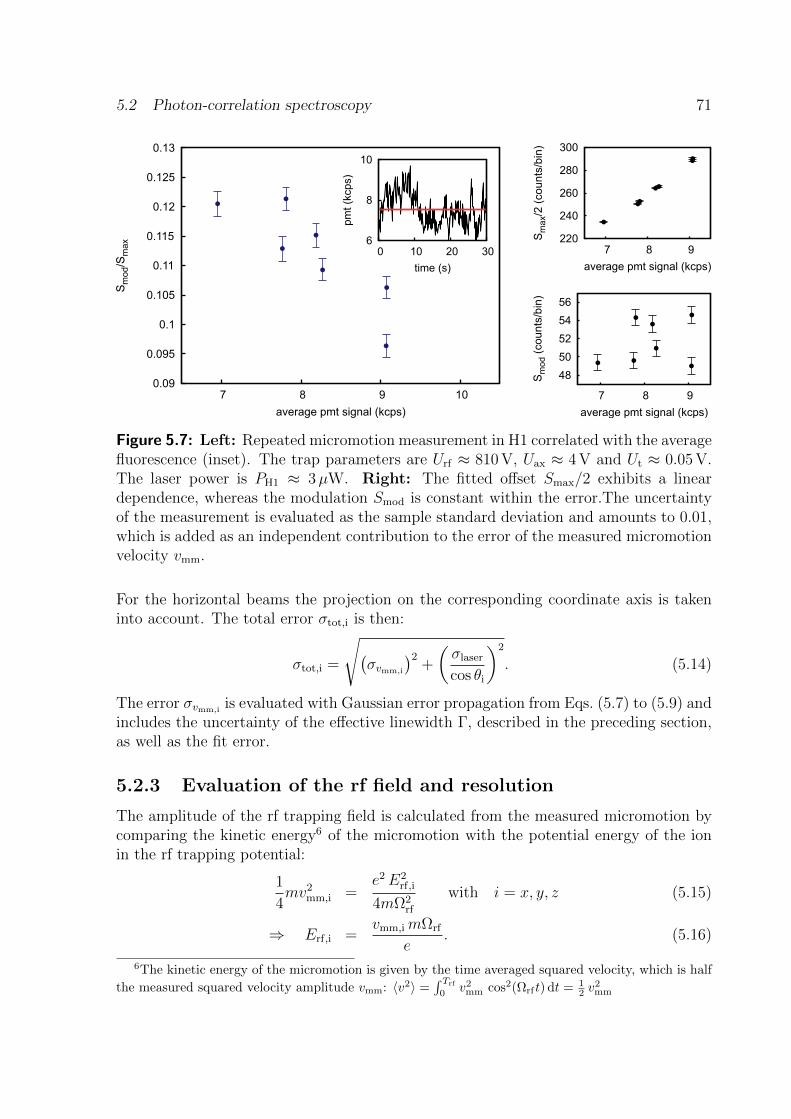
5.2 Photon-correlation spectroscopy 71
220
240
260
280
300
320
7 8 9 10
Sm
ax/2
(co
un
ts/b
in)
average pmt signal (kcps)
6
7
8
9
10
11
7 8 9 10
Sm
od
(counts
/bin
)
average pmt signal (kcps)
6
8
10
0 10 20 30
pm
t (k
cp
s)
time (s)
0.01
0.015
0.02
0.025
7 8 9 10
Sm
od/S
ma
x
average pmt signal (kcps)
48
50
52
54
56
7 8 9
Sm
od
(co
un
ts/b
in)
average pmt signal (kcps)
220
240
260
280
300
7 8 9
Sm
ax/2
(co
un
ts/b
in)
average pmt signal (kcps)
0.09
0.095
0.1
0.105
0.11
0.115
0.12
0.125
0.13
7 8 9 10
Sm
od/S
ma
x
average pmt signal (kcps)
Figure 5.7: Left: Repeated micromotion measurement in H1 correlated with the averagefluorescence (inset). The trap parameters are Urf ≈ 810 V, Uax ≈ 4 V and Ut ≈ 0.05 V.The laser power is PH1 ≈ 3µW. Right: The fitted offset Smax/2 exhibits a lineardependence, whereas the modulation Smod is constant within the error.The uncertaintyof the measurement is evaluated as the sample standard deviation and amounts to 0.01,which is added as an independent contribution to the error of the measured micromotionvelocity vmm.
For the horizontal beams the projection on the corresponding coordinate axis is takeninto account. The total error σtot,i is then:
σtot,i =
√(σvmm,i
)2+
(σlaser
cos θi
)2
. (5.14)
The error σvmm,iis evaluated with Gaussian error propagation from Eqs. (5.7) to (5.9) and
includes the uncertainty of the effective linewidth Γ, described in the preceding section,as well as the fit error.
5.2.3 Evaluation of the rf field and resolution
The amplitude of the rf trapping field is calculated from the measured micromotion bycomparing the kinetic energy6 of the micromotion with the potential energy of the ionin the rf trapping potential:
1
4mv2
mm,i =e2E2
rf,i
4mΩ2rf
with i = x, y, z (5.15)
⇒ Erf,i =vmm,i mΩrf
e. (5.16)
6The kinetic energy of the micromotion is given by the time averaged squared velocity, which is half
the measured squared velocity amplitude vmm: 〈v2〉 =∫ Trf
0v2
mm cos2(Ωrft) dt = 12 v
2mm

72 CHAPTER 5 Characterization of prototype trap
In the same way the error for the rf field is obtained.Summarizing, the resolution of the photon-correlation spectroscopy is evaluated in
units of the rf electric field. The highest resolution is obtained for the micromotion ycomponent measured along laser beam V with a scatter of σrf,y = 21 V/m due to theuncertainty σlaser. For the measurements along the trap axis this uncertainty is 22 V/m.The lowest resolution is obtained in x direction with σrf,x = 49 V/m. The fit to the datacontributes an additional statistical uncertainty of 8 V/m.
As an example, Fig. 5.8 shows the histograms of two measurements of the radialmicromotion component along the y-axis of a single ion as measured by the laser beamalong V.
300
330
360
390
0.3 0.6 0.9 1.2 1.5 1.8
nu
mb
er
of
eve
nts
T (2p / Wrf)
270
300
330
360
390
0.3 0.6 0.9 1.2 1.5 1.8
nu
mb
er
of
eve
nts
T (2p / Wrf)
a) b)
Figure 5.8: Photon-correlation signal of micromotion along y direction as measured withvertical laser beam (V). The acquisition time is 30 s. a) Ion with optimized micromotion.Restricting the phase to −π/2 < ϕi < π/2 the fit yields Smod/Smax = 0± 0.0017. b) Ionshifted by ∆Uec = 5.8 mV (corresponding to ∆x = 57 nm) in x direction. The red line isa sine fit to the data with Smod/Smax = 0.011± 0.0016.
As shown in Fig. 5.8, an electric field of ∆Ex = 0.9 V/m, corresponding to ∆Uec =5.8 mV, has to be applied to produce a detectable micromotion along the y-axis. Thiscorresponds to an rf field amplitude of Erf,x = (51± 23) V/m, or an excess micromotionamplitude of 1.1 nm. With (∆ν/ν)mm = −〈v2
mm〉/2c2, this gives a relative frequencyshift due to time dilation of −8.5 × 10⁻²⁰. Here, the resolved rf field is limited onlyby the resolution of the dc voltage control on the electrodes that move the ion radially.It is worthwhile mentioning that the rf field induced Stark shift is about an order ofmagnitude smaller than the shift due to time dilation, as shown in [19], and thereforenegligible in this work.
5.3 Micromotion in the trap
5.3.1 Radial micromotion
To characterize and test the photon-correlation method quantitatively, a single ion wasfirst shifted in both radial directions of the trap, where the strong rf quadrupole potential

5.3 Micromotion in the trap 73
dominates and its field gradients can be determined accurately from the measurementsof the secular frequencies. In Fig. 5.9a the micromotion measurement is shown for anion shifted along the y direction and in Fig. 5.9b for an ion shifted along the x direction.
a) b)
0
100
200
300
400
-0.4 -0.2 0 0.2 0.4
|Erf
,y(x
)|
(V/m
)x position (µm)
0
200
400
600
800
1000
-0.9 -0.6 -0.3 0 0.3 0.6 0.9
|Erf
,x(y
)|
(V/m
)
y position (µm)
Figure 5.9: RF field as function of ion displacement in radial directions x and y. To checkthe consistency of the measured micromotion amplitudes, expected rf field amplitudeshave been calculated from the measured radial secular frequencies (solid lines). In b)the measured field gradient is obtained by a linear fit (light blue line) to estimate thedeviation from the calculated value.
The graphs show the measured rf electric field component perpendicular to the di-rection of the ion shift as a function of the ion position in the trap. The position of theion is calculated according to Eq. 2.12 using the measured radial secular frequencies ωi
and the calculated dc electric fields Ei applied by changing Utc and Uec, see Tab. 3.4.The secular frequencies have been measured in Sec. 5.1.2 in the direction of the principalaxes. Taking the average of these frequencies leads to a good approximation for theactual frequency in x and y direction used here, which amounts to ωx,y ≈ 2π × 482 kHz.
For comparison, the rf electric field obtained by the FEM calculations is plottedtogether with the measured data as a function of the ion position. The measurement ofthe x component of the field is in good agreement with the calculation. However, they component shows a deviation, which is evaluated by fitting the function |Erf,y(x)| =∇Erf,y |x| to the data, yielding a field gradient of ∇Erf,y = (1.01 ± 0.01) × 109 V m−2,which gives a deviation of about 25 % from the calculated value.
This discrepancy can be explained by the fact that the Rogers 4350BTM boards areelastic. Pictures taken from the assembled trap stack show that the outer compensationboards slightly bend away from the rf trap boards in the center and therefore have alarger distance to the trap center in the x direction. This leads to a decreased staticelectric field at a given compensation voltage Uec. An FEM calculation, in which thedistance between the compensation and trap boards is varied, shows a decrease of thedc field in x direction of about 30 % for an increase of the electrode distance from thespacer thickness tsp = 250µm to about 500µm, which is reasonable looking at the takenpictures, see Fig. 5.10a.

74 CHAPTER 5 Characterization of prototype trap
-160
-150
-140
-130
200 300 400 500 600
Ex(x
) (V
/m)
electrode distance (µm)
b)a)
Figure 5.10: a) Picture of the laser cut trap from the rf side. The compensation boardsare bent away from the trap boards in the center compared to the edges, where the dis-tance is given by the thickness of the spacers. b) In FEM calculations, one compensationelectrode array is shifted away from the rf ground electrodes, the compensation voltageis Uec = 1 V. From a distance equal to the spacer thickness of 250µm to about 500µmthe field in the trap center decreases by about 15 %. With one or two compensationboards bent away, the x component of the compensation field Eec can decrease to about30 %, which gives a possible explanation for the discrepancy between measured data andcalculation in Fig. 5.9.
On the other hand, along the y direction the ion is shifted by applying Utc on the rfground electrodes on the quadrupole trap boards. As these electrodes are more rigidlymachined from one continuous wafer and measured secular frequencies have confirmedthe expected rf quadrupole geometry, no relevant deviations in the applied dc fields,created by Utc, are expected here. This gives a strong argument for the good agreementbetween the measurement and the calculations in the case of the vertical ion shift, whereErf,x is measured.
5.3.2 Axial micromotion
To measure residual rf fields, a single ion was shifted in the direction of the trap axis andthe micromotion was measured in all dimensions. The laser beams have been adjustedwhile shifting the ion, in order to prevent systematic uncertainties due to a change inthe intensity at the ion position.
The axial rf field is shown in Fig. 5.11 and compared to FEM calculations, thatinclude the contribution to the rf electric field due to the finite length of the trap as wellas the slits between the electrodes, see Fig. 5.12.
In the calculations the dominant contribution to the axial field component is dueto the electrode gaps with an estimated field gradient of about 1.5 × 10³ V m−2 U−1
rf .Compared to this, the contribution due to the finite length of the trap is much lowerwith about 5.1 V m−2 U−1
rf . Adding up these values and multiplying it with the measuredrf voltage of about 810 V a gradient of ∇Ez,calc = 1.22 × 10⁶ V m−2 is compared to the

5.3 Micromotion in the trap 75
0
50
100
150
200
250
300
350
400
-150 -100 -50 0 50 100 150 200 250 300
|Erf
,z(z
)|
(V/m
)
axial position (µm)
Figure 5.11: Residual axial rf electric field along trap axis derived from measured mi-cromotion amplitude (diamonds) compared to axial rf field estimated from FEM calcula-tions (solid black line), yielding a gradient of ∇Ez,calc = 1.22× 10⁶ V m−2 at Urf = 810 V.The blue line indicates the function fitted to the data: Erf,z(z) = ∇Erf,fit |z − z0|, with∇Erf,fit = (1.74 ± 0.05) × 106 V m−2 and z0 = 100µm. The dashed line indicates the rffield, for which the relative frequency shift induced by micromotion is smaller than 10−18
for an indium ion optical clock. The zero axial position corresponds to the ion positionfor Uax,1 = Uax,3 = 4 V, where the measurement was initiated.
measured value of ∇Ez,fit = (1.74± 0.05)× 106 V m−2, see Fig. 5.11.
Alignment and machining uncertainties and their effect on the rf field have beeninvestigated in [19] and presented in Ch. 2. According to that, variations in the width ofthe slits between the electrodes due to machining tolerances would affect the measuredfield gradient and can be an explanation for the slightly larger measured rf fields.
In order to determine the residual field in all dimensions, the radial components havebeen measured together with the axial component, see Fig. 5.13. With this an rf field of115 V/m or below could be verified in the range of 40 < z < 170µm in all dimensions.
The sudden change in the range z ≈ 0...75µm in both graphs can be explained bychanges of the trapping potential over a two-day measurement after compensating themicromotion only in the beginning. These can be caused by stray fields due to slowlyvarying patch potentials over night. Since the measurements were done in the centralsegment, the adjacent loading segment, which provides axial confinement could also havebeen contaminated when loading a new ion.
Besides that, a deviation of 100µm was observed between the ion position withminimum micromotion and the average ion position for symmetric axial dc voltagesUax,1 = Uax,3 = 4.0 V, which is at z = 0 in Fig. 5.11. This can be due to angularmisalignment of the trap boards, leading to an offset in the axial rf field in the trappingregion [19], machining tolerances of the electrode notches or dc stray fields, shifting theion from their average position in the axial trapping potential. These effects are notdistinguishable in the present setup.

76 CHAPTER 5 Characterization of prototype trap
-1
-0.5
0
0.5
1
-4 -2 0 2 4
Ez(z
) (V
/m)
z (mm)
Figure 5.12: Calculated axial rf field of the laser cut trap for an rf voltage Urf =1 V. Compared are the contributions of the electrode gaps (dark blue line) with thecontribution due to the finite length of the electrodes (red line). A linear fit (green line)to the linearly increasing field in the trap center yields a value for the field gradientof (1.50 ± 0.01) × 103 V m−2 U−1
rf , which corresponds to the black line in Fig. 5.11 forUrf = 810 V. The finite length leads to a field gradient of about (5.11± 0.03) V m−2 U−1
rf .The dashed light blue lines indicate the trap trap electrodes as used in the calculations.
a) b)
0
50
100
150
200
250
-150 -75 0 75 150 225
|Erf
,y(z
)|
(V/m
)
axial position (µm)
0
50
100
150
200
-150 -75 0 75 150 225
|Erf
,x(z
)|
(V/m
)
axial position (µm)
Figure 5.13: Residual radial rf field along the trap axis measured together with the axialfield component. The x component is shown in a), the y component is shown in b). Themeasurements are done over two days, with the same trap parameters and compensationvoltages. The offset of the data between z ≈ 0...75µm compared to the rest can be dueto a slow drift in the compensation over night. The red line again indicates the level atwhich the micromotion induced fractional frequency shift amounts to 1× 10⁻¹⁸.

5.3 Micromotion in the trap 77
For optical clock operation with In+ ions, the amplitudes of axial rf fields need tobe |Erf | < 115 V/m to guarantee a small enough fractional frequency shift due to timedilation of |(∆ν/ν)mm| = 4E2
rfe2/(m2Ω2
rf) ≤ 1 × 10⁻¹⁸. In the laser cut trap a lengthof ≈ 130µm is found for an rf voltage of 810 V, within which this condition is fulfilled.At full rf amplitude of 1500 V, this length is reduced by about a factor of two, allowingspace for about 12 trapped ions.
For comparison the axial rf field has been measured in the milled trap as well. InFig. 5.14 the results are compared to the measurement and the FEM calculation in thelaser cut trap.
0
100
200
300
400
500
-250 -200 -150 -100 -50 0 50 100 150 200
|Erf
,z(z
)|
(V/m
)
axial position (µm)
0
100
200
300
400
500
-250 -200 -150 -100 -50 0 50 100 150 200
|Erf
,z(z
)|
(V/m
)
axial position (µm)
Figure 5.14: Residual axial rf field measured in milled trap (red circles) and comparedto the measurements (blue diamonds) and calculations in the milled trap (dashed redline) and in the laser cut trap (black line). The data are fitted (solid red line) with|Erf,z(z)| = ∇Erf,z |z| yielding a field gradient ∇Erf,z = (3.4± 0.2)× 106 V m−2, which isa factor of two higher than in the laser cut trap.
A linear fit to the data yields a field gradient in the milled trap of ∇Erf,z = (3.4 ±0.2)× 106 V m−2, which is a factor of two higher than the gradient measured in the lasercut trap. An FEM calculation of the milled trap was done using the measured valuesfor the slit width and segment length, see Sec. 3.3. A fit to the numerical data yields anaxial field gradient of ∇Erf,z = (1.56±0.01)×106 V m−2 at Urf = 810 V. Here, the thickerwafers reduce the axial field component, whereas the larger gaps between the electrodesincrease the axial field (see Sec. 2.4 and [19]), which causes the slight difference to thelaser cut trap for a geometry without machining tolerances.
Comparing the two traps, it is found that the laser cut trap (milled trap) exhibits anincrease in axial field gradient of about a factor 1.4 (1.8). A possible explanation for thisdifference can be machining quality of the milled wafers, as demonstrated in Fig. 3.6,leading to higher uncertainty of the slit width and therefore a larger contribution to theaxial rf field. In fact, the scatter of the measured slit widths is about a factor of twoworse for the milled trap compared to the laser cut trap.

78 CHAPTER 5 Characterization of prototype trap
0
25
50
75
100
-150 -100 -50 0 50 100 150
|Erf
,y(z
)|
(V/m
)
axial position (µm)
a) b)
0
50
100
150
200
-150 -100 -50 0 50 100 150
|Erf
,x(z
)|
(V/m
)
axial position (µm)
Figure 5.15: Residual radial rf field measured in the milled trap together with the axialcomponent. In a) the x component is shown and in b) the y component. As in the lasercut trap, here the radial field is below the value of 115 V m−1 in the region of the axialzero crossing.
As a control measurement the radial components of the rf field have been measuredtogether with the axial field in the milled trap, see Fig. 5.15.
5.3.3 Longterm analysis of micromotion compensation
In the laser cut trap the changing of micromotion compensation over time has beenrecorded in different measurements. One was carried out over several hours within oneday including reloading the ion twice, in order to determine changes of the micromotioncompensation due to contamination of the trap electrodes from the atomic beam. Com-pared are measurements in the loading segment and in the central segment: see Fig. 5.16.The trap parameters are Urf ≈ 810 V, Ut ≈ 0.05 V, Uax ≈ 4 V, Utc,3 ≈ −0.0552 V andUec,3 ≈ 0.3497 V, Utc,2 ≈ −0.0060 V and Uec,2 ≈ 0.6870 V. The saturation parameter ineach cooling laser beam is s ≈ 0.6.
Plotted are the micromotion components in all dimensions in both segments, as wellas the oven current to indicate the loading events. First, the data in the loading segmentare discussed.
For the vertical component, which is sensitive to ion shifts in horizontal direction, aslow drift over about four hours is observed. The other two components do not exhibitany drift. At the beginning of the measurement, the oven was running for about 15minutes at medium current, which is sufficient for atomic scans and loading of single ions,initializing the experiment. Eventually, the micromotion amounts to about 150 V m−1.
At 16:00h, this micromotion was minimized by changing the compensation voltage by∆Uec = 20.3 mV, which corresponds to a dc field of ∆Edc,x ≈ 3.2 V m−1. Directly afterthe compensation a new ion is loaded with the oven running for about five minutes, toinvestigate the influence of a loading event. No change in micromotion in all componentsis observed within the resolution.
About one hour later the oven is turned on again, this time for a longer period.

5.3 Micromotion in the trap 79
0
50
100
150
11
:00
12
:00
13
:00
14
:00
15
:00
16
:00
17
:00
18
:00
19
:00
0
1
2
3
4
5
6
7
|Erf
,x| (V
/m)
I ove
n(A
)
0
15
30
45
60
11
:00
12
:00
13
:00
14
:00
15
:00
16
:00
17
:00
18
:00
19
:00
0
1
2
3
4
5
6
7
|Erf
,z| (V
/m)
I ove
n(A
)
0
50
100
150
11
:00
12
:00
13
:00
14
:00
15
:00
16
:00
17
:00
18
:00
19
:00
0
1
2
3
4
5
6
7
|Erf
,y| (V
/m)
I ove
n(A
)
DU = 20.3mVec
Figure 5.16: Longterm micromotion measurement in the loading segment (circles) andthe central segment (triangles). In between, single ions are loaded to test the influenceof atomic contamination of the trap electrodes on the micromotion compensation inthe loading segment as well as in the central segment (red triangles). For the centralsegment a measurement from the preceding day is shown (blue triangles). The ovencurrent (orange line) is indicated to mark the time for loading a new ion. Top: Thevertical micromotion component, controlled by Uec. The jump of the measured values ataround 16:00 is due to minimization of the micromotion applying ∆Uec = 20.3 mV, whichcorresponds to a dc electric field of about ∆Ex ≈ 3.2 V m−1. Center: The horizontalradial micromotion component. Bottom: The axial micromotion component.

80 CHAPTER 5 Characterization of prototype trap
After eventually loading an ion and switching off the oven a small drift of the measuredmicromotion is observed in both radial components, comparable to the drift observedearlier in the vertical component.
Looking at the micromotion in the central segment, however, shows no change withinthe measurement resolution in all components. The data points taken on the precedingday exhibit the same values as well.
From this, it can be said that loading of single ions does not influence the micromotioncompensation significantly. The observed drifts are on the order of the measurementresolution and do not allow a quantitative statement.
In the central segment the influence of the oven is negligible for this measurementas one would expect, since here the electrodes do not get contaminated. The onlychange one might expect to see is in the axial micromotion component, because thecontaminated loading segment provides axial confinement for the central segment. Butstray fields in this order of magnitude do not shift the ion axially at a detectable level inthis trap. In principle, the radial micromotion compensation voltages inhibit crosstalkto neighbouring segments. As shown in the next section, dc fields of this magnitude arealso not detectable in neighbouring segments.
Furthermore, a heating of the trap due to constantly applying rf power does not showany visible effect on the micromotion compensation on this time scale, since this wouldaffect the whole trap geometry and therefore the compensation in all trap segments. Thedrifts observed in this measurement only occur in the loading segment, see Fig. 5.16.
Another observation of the micromotion compensation was done over 41 days, mea-suring the micromotion in all dimensions at fixed trap parameters and compensationvoltages in the central segment. The parameters are the same as in the measurementdescribed before, the compensation voltages are Uec ≈ 0.552 V and Utc ≈ −0.013 V. Themeasured micromotion is shown in Fig. 5.17.
Within the plotted period of 41 days a maximal drift of about 100 V m−1 per day isobserved in all components. For the x component there is drift showing up at the endof the period indicating, that the vertical compensation changes. For the y componentall data points except the one from February 25th are constant within the resolution.
This demonstrates, that even over several days containing many loading events themicromotion compensation stays optimized, an important feature of the trap, for anapplication in clock spectroscopy.
The last analysis shows the dc compensation voltages obtained after minimizingmicromotion recorded over several months. Compared are again the loading segmentand the central segment, see Fig. 5.18.
For both segments the largest drift is observed in both dimensions between the mea-surements in the beginning of the year and the beginning of July. For the x componentsthe optimal compensation field changes by about 35 V m−1 in both segments. This canbe explained by the bake out of the apparatus in April, which was carried out with thetrap in the vacuum chamber, see Sec. 4.4. Due to heating, expansion of the elastic trapboards leads to deformation of the trap stack, therefore changing the distance betweenthe electrodes in x direction.
The drift of the compensation fields in the y direction is different for the two segments.

5.3 Micromotion in the trap 81
a) b)
100
150
200
250
17
Fe
b
27
Fe
b
08
Ma
r
18
Ma
r
28
Ma
r
|Erf
,z| (V
/m)
c)
0
50
100
150
200
17
Fe
b
27
Fe
b
08
Ma
r
18
Ma
r
28
Ma
r
|Erf
,y| (V
/m)
0
100
200
300
400
17
Fe
b
27
Fe
b
08
Ma
r
18
Ma
r
28
Ma
r
|Erf
,x| (V
/m)
Figure 5.17: Measured micromotion at fixed parameters in the central segment over 41days. The trap voltages are Urf ≈ 810 V, Ut ≈ 0.05 V and Uax ≈ 4 V. The compensationvoltages are Uec ≈ 0.552 V and Utc ≈ −0.013 V. Shown are the a) x component, b) zcomponent and c) y component.

82 CHAPTER 5 Characterization of prototype trap
a)
70
80
90
100
110
120
1300
1 F
eb
01
Ma
r
01
Ap
r
01
Ma
y
01
Ju
n
01
Ju
l
01
Au
g
01
Se
p
01
Oct
10
20
30
40
50
Edc,x
(V/m
)
Edc,y
(V/m
)
b)
90
100
110
120
130
01
Fe
b
01
Ma
r
01
Ap
r
01
Ma
y
01
Ju
n
01
Ju
l
01
Au
g
01
Se
p
01
Oct
14
15
16
17
18
19
20
Edc,x
(V/m
)
Edc,y
(V/m
)
Figure 5.18: Compensation dc fields after minimizing micromotion recorded over severalmonths in the a) loading segment and b) central segment. Plotted are the dc fieldscalculated from the applied compensation voltages. The blue circles indicate the xcomponent, the red triangles indicate the y component. In April the whole apparatus wasbaked at a temperature between 65...100 C for two weeks (orange bar). In Septemberthe trap operated over night, in total for ≈ 34 hours (green bar).

5.3 Micromotion in the trap 83
In the loading segment a drift of about 25 V m−1 similar to the x component is observed,whereas in the central segment only 5 V m−1 difference are measured. This differentialchange can be due to desorption of atomic ytterbium from the loading segment electrodeduring the bake out, since only the loading segment is contaminated and the thermalexpansion of the trap stack is much less in y direction.
After the bake out the compensation fields drift differently for the two segments.At first, it looks like the expansion of the trap boards is reversed until the beginningof September in both segments. Only the y component in the loading segment startsagain to drift in the opposite direction due to new contamination of the electrodes. Afterthis, the values change only at a small rate, except for a sudden jump between two daysobserved in the central segment. This is possibly due to the fact that the trap was leftrunning over night in order to test trapping times for a single ion. The return of thecompensation voltages on September 30th almost back to the value before the two-daymeasurement implies a relaxation of the trap due to switching off the trap drive at nightagain.
5.3.4 Measurement crosstalk of compensation voltages
The crosstalk of compensation voltages to neighbouring segments was investigated in thelaser cut trap using photon-correlation spectroscopy. For this, a single ion was loadedand trapped in the central segment and the micromotion measured as a function of thecompensation voltages in the loading segment. For normalization the micromotion wasmeasured while changing the compensation voltages of the central segment. The trapand laser parameters are the same as in the previous measurements. In Fig. 5.20 theresults for changing Utc,2 and Utc,3 are shown. The data in each radial direction are fittedwith linear functions. An example is given for the measured x component due to Utc:∣∣∣E(i)
rf,x
(U
(i)tc
)∣∣∣ = s(i)x U
(i)tc , (5.17)∣∣∣E(i)
rf,x
(U
(i+1)tc
)∣∣∣ = s(i+1)x U
(i+1)tc , (5.18)
with the index i of the segment where the compensation voltage is applied. From theratio of the slopes s
(i)x and s
(i+1)x the relative crosstalk ctc,x of Utc to the neighbouring
segment is obtained:
ctc,x =s
(i+1)x
s(i)x
. (5.19)
This procedure is in the y direction similarly. The error is calculated using Gaussianerror propagation. The results are presented in Tab. 5.3 and compared with FEM cal-culations. In the calculations the dc field components in the neighbouring segments arecompared to each other directly, see Fig. 5.19. Thus, it is important to keep in mind,that the rf electric field components are measured orthogonal to the shifting dc fieldcomponent.

84 CHAPTER 5 Characterization of prototype trap
Table 5.3: Cross-talk of compensation voltages Utc,3 and Uec,3 measured with a singleion in segment 2 and compared to FEM calculations. The measured rf field component isorthogonal to the shifting dc field component, thus the calculated dc field in x directionis compared to the measured rf field y component and vice versa.
measured values calculated calculated
(z = 0) (z = 300µm)
ctc x 0.007± 0.001 0.015 0.006
y 0.005± 0.001 0.019 0.007
cec x 0.073± 0.005 0.09 0.06
y 0.12± 0.10 0.05 0.01
The same procedure was applied for changing Uec, see Fig. 5.21 and the results aregiven in Tab. 5.3 as well.
The comparison of the measured data to the calculated values shows a differenceof up to a factor of four in the case of Utc. This can be explained by looking at thecalculation of the electric field along the trap axis, when applying a voltage in segment3. An example for Utc is given in Fig. 5.19, in which both radial field components areplotted along the trap axis for x = y = 0 over all three inner segments.
0
100
200
300
400
500
600
700
-3 -2 -1 0 1 2 3
Ex,y
(V/m
)
z coordinate (mm)
0
5
10
15
20
-0.1 0 0.1 0.2 0.3 0.4
Ex,y
(V/m
)
z coordinate (mm)
Figure 5.19: FEM calculation of the dc field, when applying Utc = 1 V in segment 3.The x (y) component is indicated by the black (red) line. The inset is a close up of theregion around the center of segment two. The relative crosstalk is obtained from the ratioof the field amplitudes at the center of each segment: cx,y = Ex,y(z = 0)/Ex,y(z = −2.2).
The estimated values for the relative crosstalk given in Tab. 5.3 are evaluated byreading the values for the field components in the center of each segment. Since the fieldhas a gradient, a region on the trap axis can be found a few hundred micrometers next

5.3 Micromotion in the trap 85
to the center, in which the calculated relative crosstalk matches the measured values,indicating that the ion may not be exactly in the center.
a)
c) d)
b)
0
50
100
150
-0.5 -0.4 -0.3 -0.2 -0.1 0
|E(3
) rf,y
| (V
/m)
Utc,3 (V)
0
50
100
150
-0.5 -0.4 -0.3 -0.2 -0.1 0|E
(3) rf
,x| (V
/m)
Utc,3 (V)
0
100
200
300
400
500
-0.02 -0.015 -0.01 -0.005
|E(2
) rf,y
| (V
/m)
Utc,2 (V)
0
150
300
450
600
-0.02 -0.015 -0.01 -0.005
|E(2
) rf,x
| (V
/m)
Utc,2 (V)
Figure 5.20: Measured rf field due to micromotion of a single ion trapped in the centralsegment (2). Plotted are the field components in x and y direction for changing Utc,2 (left)and Utc,3 (right). For the fits in the loading segment (3) the data at Utc,3 = −0.05 V arenot included, since around this value the micromotion is minimized and scaling cannotbe observed. The fitted slopes in x direction are: a) s
(x)tc,2 = (−46.3±4.6)×103 V m−1 U−1
tc,2
and b) s(x)tc,3 = (−240±57) V m−1 U−1
tc,3, as well as in y direction: c) s(y)tc,2 = (−40.5±3.4)×
103 V m−1 U−1tc,2 and d) s
(y)tc,3 = (−282± 15) V m−1 U−1
tc,3.

86 CHAPTER 5 Characterization of prototype trap
a)
c) d)
b)
0
100
200
300
0 0.1 0.2 0.3 0.4 0.5
|E(3
) rf,y
| (V
/m)
Uec,3 (V)
0
50
100
150
-0.1 0 0.1 0.2 0.3 0.4
|E(3
) rf,x
| (V
/m)
Uec,3 (V)
0
100
200
300
400
500
0.65 0.66 0.67 0.68 0.69 0.7
|E(2
) rf,y
| (V
/m)
Uec,2 (V)
0
50
100
150
200
0.5 0.55 0.6 0.65
|E(2
) rf,x
| (V
/m)
Uec,2 (V)
Figure 5.21: Measured micromotion of a single ion trapped in the central segment (2).Plotted are the micromotion components in x and y direction for changing Uec,2 (left)and Uec,3 (right). In d) the data at Uec,3 = 0.5 V is not included in the fitting range.The fitted slopes in x direction are: a) sec,2 = (354 ± 120) V m−1 U−1
ec,2 and b) sec,3 =
(43 ± 34) V m−1 U−1ec,3, as well as in y direction: c) sec,2 = (−9.0 ± 0.5) × 103 V m−1 U−1
ec,2
and d) sec,3 = (−663± 35) V m−1 U−1ec,3.

Chapter 6
Structural phase transitions andtopological defects in Coulombcrystals
With the prototype trap introduced in the preceding Chapters it was possible to carry outmeasurements on the dynamics of 172Yb+ Coulomb crystals during symmetry breakingphase transitions. This section details on the work presented in Pyka et al. [57].
First, a brief review and historical background of symmetry breaking phase tran-sitions is given to introduce the physical background of the presented measurements.The Kibble-Zurek mechanism (KZM) is introduced as a possible scenario to predict thescaling of the rate of defect formation with the rate at which the transition is driven.Moreover, it tries to predict this scaling in a universal manner, such that it is applicableto a wide range of physical systems.
The second section focuses on the structural phase transition from a linear Coulombcrystal to a two dimensional “zigzag” configuration and gives the relevant equations de-rived in accordance with the theoretical model of phase transitions elaborated by Landauand Ginzburg. The KZM extends this model and includes non-equilibrium dynamics atthe critical point of the transition to explain the formation of topological defects (in thefollowing referred to as kinks) when the system changes from the symmetric (linear) tothe symmetry-broken (zigzag) phase.
Numerical simulations are described in Sec. 3, that are carried out in order to find arange of experimentally feasible parameters as well as provide simulated data that maybe compared to measurements. Furthermore, the dynamics of the kinks are investigated.
In Sec. 4, the experimental setup and measurement scheme are described in detail,focusing on the evaluation of the quench parameter, as well as the methods for analysisof the obtained data.
In the last section the analysis of the experimental data is presented. The measureddata are compared to the simulated data and the observed scaling is analyzed.
87

88 CHAPTER 6 Phase transitions and defects in Coulomb crystals
6.1 Introduction to the field
Phase transitions are ubiquitous in nature, from the melting of ice to condensed mat-ter, super fluidity, formation of magnetic domains or phenomena in cosmology [58–62].Intriguing is the fact that the behaviour of such different systems in phase transi-tions exhibits universal characteristics that can be described by the same mathematicalmodel. So far, this has lead to a comprehensive effort of studies in a wide range ofsystems [62–67].
A successful phenomenological approach to describe phase transitions is based ontheoretical work of Landau and Ginzburg [68, 69]. Here, the important properties thatdetermine the behaviour of a system near a phase transition are the relaxation time, as ameasure of the rate at which the system returns to its thermodynamic equilibrium, andthe correlation length, as a measure for the scale at which fluctuations affect the system.Phase transitions are characterized by the divergence of the relaxation time as well asthe correlation length in the vicinity of the critical point at which the transition occurs.
Because this diverging correlation length becomes much larger than the interatomicspacing of a system, its microscopic properties become less important and the behaviourof the system can be described by universal scaling laws that are represented the criticalexponents [68]. Furthermore, the system exhibits anomalous static and dynamic physicalproperties near the critical point, for example the formation of local defects in the globallyordered structure of the symmetry broken phase of the system after the quench (changein a control parameter of the system that induces the phase transition).
Kibble proposed a scenario like this in the beginning of the universe during the coolingdown and expansion after the Big Bang [58,59] to understand its current structure. Theidea was that fluctuations in the system freeze out when the temperature went under acritical value, including temporary defects in the structure. These defects occur becausethe fluctuations can only propagate within causally connected regions1 (domains) beforethe freeze-out. After passing the critical point, the domains relax independently to thenew state, stabilizing the defects. In his work he attempted to predict a scaling law ofthe formation of defects depending on the quench rate with which the phase transitiontakes place. However, since he assumed thermal equilibrium of the system, he found thecreation of defects for the most part independent of the quench rate.
Zurek took over this idea and additionally took into account the non-equilibriumnature of phase transitions. His argument was that the actual value of the correlationlength at the freeze-out time is determined by the rate at which the system can followthe quench, which is maximal at the freeze-out time. Like this the correlation lengthas a scale for the formation of defects is related to the quench rate. Based on thisconcept the Kibble-Zurek mechanism has been investigated theoretically in a variety ofsystems [60,70–72].
Several experimental approaches were successful in demonstrating defect formationin homogeneous systems [62, 73, 74], but weak dependence on the transition rate andlimited control over external parameters so far prevented conclusive results on KZM
1Here, Kibble introduces the size of domains as the distance on which fluctuations travel at the speedof light within the critical freeze-out time.

6.2 Theoretical description 89
related scaling of defect formation. Another difficulty in comparing experiment with thetheory is the task of determining the critical exponents of a system in order to give arealistic prediction of the scaling coefficient. Recent predictions for KZM scaling focuson inhomogeneous systems, in which the critical point is reached at different instancesfor different positions, in contrast to homogeneous systems. An illustrative example ofeach system type is given by the linear to zigzag transition of ions confined in a ringtrap (homogeneous) or a linear trap providing three dimensional harmonic confinement(inhomogeneous). The latter is illustrated in Fig. 6.1.
Formation of defects
quench
vF
Breaking the symmetry
p/2
p/2
1-p
Figure 6.1: Illustration of a structural phase transition in a Coulomb crystal. Left:Release of the radial confinement at constant axial potential leads to a change from linearto “zigzag” configuration with lowest potential energy. The system undergoes a phasetransition from a symmetric to a symmetry broken phase. In this finite inhomogeneoussystem the phase transition occurs first in the center of the chain and propagates on afront with velocity vF to the ends of the crystal. Right: Depending on the front velocitythe system chooses different configurations in the symmetry broken phase. Here, threeoutcomes are shown: a kink (anti-kink) in the top (bottom) or a regular “zigzag” withoutdefects in the middle.
Here, due to the inhomogeneous inter-ion spacing, the phase transition first occurs inthe center of the ion chain and moves out to the ends on a critical front. These dynamicsenhance the role of causality and steepen the scaling of the rate of defect formation withthe transition rate as predicted recently for various systems [71,75–77].
In the presented work the defect density is measured as a function of the quench ratefor the linear to zigzag transition in 172Yb+ Coulomb crystals using the experimentalsetup introduced in the preceding chapters. The experimental data are supported withnumerical simulations at the experimental parameters. The results give rise to questionsabout new physical regimes in which a modification of KZM scaling is possible [74] withrespect to the predictions made in del Campo et al. [71].
6.2 Theoretical description
In the presence of laser cooling, such that the kinetic energy becomes smaller than theCoulomb force-induced interaction energy, ions confined in a harmonic potential arrange

90 CHAPTER 6 Phase transitions and defects in Coulomb crystals
into a crystal-like structure (Coulomb or Wigner crystal) exhibiting collective dynamics,which dominate the behaviour of the ensemble.
The particular structure depends on the interplay between the trap potential pushingthe ions together and the counteracting Coulomb potential. The Hamiltonian of thesystem is:
H(r, t) =
Nion∑i=1
(m2
r2i
)+ Etrap + Ecoul, (6.1)
with Etrap =
Nion∑i=1
[m2
(ω2
x,i x2 + ω2
y,i y2 + ω2
z,i z2)], (6.2)
and Ecoul =e2
4πε0
Nion∑i<j
1
|ri − rj|. (6.3)
In order to minimize their potential energy the ions arrange into a structure thatdepends only on the ratio of the secular frequencies transverse to and in the directionof the symmetry axis. For a tight radial confinement the ions line up on the trap axisforming a chain. For constant axial confinement when lowering the radial trap frequency,at a certain point the ions experience an effective saddle-point potential [78] and the chainbecomes unstable. Eventually the ions rearrange into a two-dimensional zigzag structure,see Fig. 6.1. Lowering the radial confinement even further leads to more complex threedimensional configurations. In Fishman et al. [79] the stability of Coulomb crystals hasbeen investigated looking at the spectrum of the normal modes of the crystal. There it isfound that the mode which first becomes unstable at the critical point is the zigzag modeand the critical frequency has been derived analytically from the dispersion relation fora homogeneous system. According to Steane et al. [80] this critical frequency can be wellapproximated for mesoscopic crystals (Nion ∼ 10...1000) by:
ωrad
ωax
= 0.73N0.86ion . (6.4)
A more important outcome of the work in Fishman et al. [79] is the demonstrationof the linear to zigzag transition to be a second order phase transition, which allows thedetermination of the critical exponents.
In homogenous systems, for example ion crystals in a ring trap, the phase transitionoccurs globally at the same instant. Here, the speed of sound is v = aωax [71], with theconstant lattice parameter a and the axial trap frequency ωax.
However, in inhomogeneous systems, for example ion crystals confined in a lineartrap as presented in this work, the critical point of the phase transition is reached locallyat different times. Here, the inter-ion distance a(z) is not constant and can be wellapproximated using the axial charge density n(z) = n(0)(1 − z2/L2) = 1/a(z) [81],with n(0) = 3
4Nion/L and the half-length of the crystal L at the axial ion position z.
Thus, with the maximal ion density in the center of the crystal, the critical point is firstreached in the middle, propagating on a front towards the ends of the crystal. From this

6.2 Theoretical description 91
it can be seen that defects can only form in a region where the front velocity is largerthan the speed of sound, which is a measure for the velocity of fluctuations propagatingthrough the crystal. This enhances the role of causality, leading to a larger scaling ofthe formation of defects.
Another characteristic systematic feature is motional damping of the fluctuationsdriving the transition, sometimes also referred to as viscosity [82]. In the case of Coulombcrystals in ion traps this damping is induced by the dissipative process of laser cooling,which can be described in terms of the friction coefficient η:
η =2s
(2 + s)2~k2, at ∆ = −Γ
2, (6.5)
with the saturation parameter s of the cooling laser, its wavenumber k and its detuning∆ with respect to the atomic transition with linewidth Γ, see [83]. As in the analogouscase of a harmonic oscillator, the dynamics of the system, and thus the scaling of defectformation, depend strongly on the friction parameter. In the overdamped case, thedynamics close to the critical point are dominated by relaxation motion due to thestrong damping. Moreover, the the density of defects do directly depends on η, as wasderived for the linear to zigzag transition in Coulomb crystals in [76]:
do ∝ηδ0
τQ
. (6.6)
Here, δ0 is the amplitude of the quench, when ramping down the transversal trappingpotential, and the quench time 2τQ is defined as half of the ramp duration.
In the underdamped regime, the dynamics is dominated by the oscillatory motion ofthe ions, leading to a scaling of the density of defects du, that is independent from thefriction coefficient η and more pronounced [76]:
du ∝(δ0
τQ
)4/3
. (6.7)
This is the regime in which the presented measurements are carried out.Both scalings shown here are derived for an ion chain confined in a harmonic potential,
obeying the inhomogeneous KZM (IKZM). The derivation is under the premise that theregion xd in which defects form is much smaller than the crystal size 2L: xd 2L,in order to obtain a power-law scaling [84]. The scaling of 4/3 (1) derived here, issignificantly enhanced compared to the scaling of 1/3 (1/4) in the homogenous KZMregime for the underdamped (overdamped) case [76].
Currently under theoretical and experimental investigation is the situation in whichthe correlation length becomes comparable to xd, in other words, where not more thanone defect is created during a quench. In this case, it is suggested that the scaling of thedensity of defects is doubled compared to the IKZM scenario:
d1 ∝(δ0
τQ
)8/3
, (6.8)

92 CHAPTER 6 Phase transitions and defects in Coulomb crystals
which has also been observed in several other systems [72,74,85].Two kinds of kinks have been identified [86] that are stable after the quench and
therefore within reach for experimental investigation, see Fig. 6.2. The “odd” kink iscreated when a single ion between two independent domains is not able to follow theconfiguration of either one during the quench and therefore remains on the symmetry axisof the zigzag stabilized by the mutual Coulomb repulsion. This configuration is stable forshallow zigzag configurations. However, when lowering the radial confinement further,the ion breaks out into one of the edges of the zigzag rearranging the crystal in a newenergetically favourable position. This configuration, with the discontinuity still present,is called “extended kink”. Because both kinks stem from the same creation mechanism,they obey the same statistics. Experimentally, these statistics cannot be recovered inevery case due to loss mechanisms, as will be discussed later in this Chapter.
20µm
Figure 6.2: Pictures of experimentally obtained kinks. Top: “Odd” kink with the twodomains separated by an ion trapped in on the symmetry axis through mutual Coulombrepulsion. This configuration is stable for shallow quenches. Bottom: “Extended” kink:here the ion dividing the two configurations moves out to one of the edges of the crystal.This is the energetically favourable position for quenches deeper into the zigzag regime.
6.3 Simulating dynamics of trapped Coulomb crys-
tals
6.3.1 Method and kink detection
Numerical simulations have been carried out to investigate the dynamics of defect for-mation during quenches of the trapping potential, as well as to identify parameters thatallow for experimental investigation [87]. For this, the trajectory of each ion during thesimulation is calculated using a Runge-Kutta 4th order algorithm2 from the equationsof motion:
mri = −ηri +∇iEtrap(t) +∇iEcoul + εi(t), (6.9)
with the stochastic force εi(t) implemented in the simulation by adding a random kick tothe velocity at each time step in order to simulate thermal kicks according to temperature
2Courtesy: Ramil Nigmatullin

6.3 Simulating dynamics of trapped Coulomb crystals 93
of the system. For the realization of the trap, the effective pseudo-potential Etrap is usedwith time-dependent radial trapping frequencies to create the quench. In this modelmicromotion and background collisions are not included. The ramp implemented is linearin the secular frequencies, see Fig. 6.3a. In the presented simulations the trajectoriesare calculated with a resolution of 1.3 ns. For evaluation of the data, however, it isadvantageous to save computational resources by using a step size of 1.3µs, since thecharacteristic time scale set by the trap frequencies is on the order of a few tens ofmicroseconds. Laser cooling is implemented as a uniform travelling wave in all threedimensions represented by the parameter η defined in Eq. 6.5, damping out the ionmotion induced by the random kicks to thermal equilibrium.
The time evolution of the system is split into two intervals, one of which representsthe quench t1 = 2τQ and the second, t2, describes the relaxation of the system afterthe quench as governed by the dissipative force of the cooling laser, see Fig. 6.3a. Toinvestigate the scaling of the kink density, the simulation is repeated several hundredtimes for each quench time and the statistics are evaluated.
The kink detector algorithm3 scans the coordinates at each time step, evaluates therelative positions of neighbouring ions along the trap axis, and gives out a function thatcan take three possible values: f(ri, ri+1) = 1, 0,−1, with i = 1...Nion−1. In a regularzigzag pattern each ion will always be on the opposite site of the symmetry axis from itsneighbours, thus giving: fzz(ri, ri+1) = (−1)i, (−1)i+1 depending on the orientation ofthe pattern. However, in the case of a kink, this alternating pattern has a discontinuity,i.e. two consecutive values with the same sign for an odd kink and a zero in the case ofan extended kink, see Fig. 6.3b.
trap axis
x
time
a) b)
t1 t +t1 2
wrad
wax
Figure 6.3: a) Scheme of the simulated quench. The ramp during t1 = 2τQ is linear insecular frequency. After the ramp the system relaxes for the duration t2. To obtain sta-tistical information this sequence is repeated between 250 and 3000 times. b) Schematicillustration of the kink detection in the simulated data. The algorithm scans the ionpositions and gives discrete values fzz(ri, ri+1) for each pair of neighbouring ions, seetext. In the case of a kink the regular zigzag pattern is interrupted, as indicated by thered lines. The outer regions of the crystal are ignored as an additional condition.
To analyze the dynamics of defects, the detection routine scans all recorded timesteps of a simulation giving two important statistical outcomes. The first is the number
3For a detailed description, see [88].

94 CHAPTER 6 Phase transitions and defects in Coulomb crystals
of kinks that are created during the quench and thus accounted for by the KZM (inthe following referred to as created kinks). The second is the number of kinks thatis accessible in the experiment (in the following referred to as surviving kinks). Theacquisition time of the camera is limited to a few tens of milliseconds, but the quenchhappens on the order of a few hundred microseconds or less. Therefore only kinks canbe observed that survive until the aquisition time. As seen in Fig. 6.4, which showssimulated kink density as a function of time, there is a plateau in the kink density afterthe quench which indicates kinks that are stable long enough to be detected by thecamera. Interestingly, this is not equal to the number of created kinks, which are partlylost due to several reasons that will be explained later.
0
0.2
0.4
0.6
0.8
0 50 100 150 200 250
Nkin
ks/N
pic
s
time (µs)
0
0.1
0.2
0.3
0 50 100 150 200 250
Nkin
ks/N
pic
s
time (µs)
0
0.005
0.01
0.015
0 100 200 300 400 500
Nkin
ks/N
pic
s
time (µs)
a) b) c)
Figure 6.4: Time evolution of the kink density in the simulations [88]. The kink detectorcounts defects at each time step of the simulation (step size: 1.3µs) for all sequenceswith the same quench time. Dividing this by the total number of quenches yields thekink density as a function of time (blue line). The quench is indicated by the red line.a) A simulation with 2τQ = 30µs. Clearly visible is the peak of kinks created during thequench and the plateau of stable kinks. b) A simulation with 2τQ = 80µs. The lossesafter the peak of created kinks is negligibly small, indicating that in this regime it shouldbe possible to measure a scaling due to KZM. c) A simulation with 2τQ = 250µs. Here,again losses are visible, this time during the quench. Reasons for the losses are given inSec.6.3.3)
6.3.2 KZM regimes
A set of simulations has been carried out for a wide range of τQ in order to find regimesthat are accessible with the experimental setup in this work, yielding the graph shownin Fig. 6.5.
Plotted are the densities of created kinks for different quench times and the axialtrap frequency ωax suggested as an experimentally feasible parameter. On the left side,for slow quenches, the scaling is comparable to the one derived in Eq. 6.8 accounting forthe DIKZM regime in which only one or no kink is created per quench. When increasingthe speed of the quench, the scaling changes to a value similar to the one given for theIKZM regime. On the right the quench is fast enough that during the entire quenchthe front velocity is higher than the sound velocity. Here, even in an inhomogeneoussystem, due to the fast quench the homogeneous KZM [76] is recovered. For even fasterquenches a plateau is reached, which is accounted for by the finite size of the system

6.3 Simulating dynamics of trapped Coulomb crystals 95
-5
-4
-3
-2
-1
0
1
-3 -2 -1 0 1 2
ln(d
)
-ln(waxtQ)
Figure 6.5: Density of created kinks plotted against quench time. For different rangesa change in the slope can be seen. On the left, for slow quenches, a steep slope of 8/3 isindicated (dashed line), suggesting kink probabilities of less than unity per realization.As the kink density increases with faster quenches, the scaling decreases to a value closeto 4/3 (solid line), as determined by the IKZM. Increasing the quench rate further leadsto a decrease of the slope to about 1/3 (dotted line) indicating that the velocity ofthe critical front exceeds the sound velocity over the whole crystal, thus recovering thehomogeneous KZM regime. The friction is η = 1.5× 10⁻²⁰ kg s−1 in this simulations.
and kink-kink interactions. As already indicated in Fig 6.4 and as will be shown in thefollowing section, not all of these regimes are accessible to the experiments.
6.3.3 Loss mechanisms
Not all regimes are accessible in the experiment for distinct reasons. A kink is stablebecause it does not have enough kinetic energy to pass a barrier, that is set by thePeierls-Nabarro potential [89], which builds up during the quench. For fast quenchesa high amount of kinetic energy is brought into the system, enough for the kink toovercome the potential barrier and leave the zigzag structure. This mechanism is foundto be sensitive to the laser cooling friction coefficient, see Fig. 6.6. The higher thedissipative force, the faster the system relaxes into thermal equilibrium, again providinga stable environment for the defects.
For slow quenches, when the speed of the front of the phase transition is comparableto the speed with which a defect can move within the ion crystal, losses can occur due tothe inhomogeneity of the system. A kink created in the central region experiences only alow potential barrier, because the zigzag pattern is not yet completely developed. Movingfaster than the front, the kink escapes the zigzag pattern to the ends of the crystal. Thismechanism does not depend on the friction, see Fig. 6.6. Looking at Fig. 6.4c, the lossesoccur within a time of about 40µs or less, which corresponds to about one oscillationperiod at the axial trap frequency of ωax/(2π) ∼ 25 kHz.

96 CHAPTER 6 Phase transitions and defects in Coulomb crystals
-7
-6
-5
-4
-3
-2
-1
0
1
-3.5 -3 -2.5 -2 -1.5 -1 -0.5
ln(d
)
-ln(waxtQ)
Figure 6.6: Kink density plotted against quench time for different friction parametersη: 1.5× 10⁻²⁰ kg s−1 (circles), 6.0× 10⁻²¹ kg s−1 (pentagons), 4.0× 10⁻²¹ kg s−1 (invertedtriangles) and 3.0 × 10⁻²¹ kg s−1 (triangles). The filled symbols show the density ofcreated kinks and the hollow symbols show the density of surviving kinks. The frictiondependent losses of created kinks for fast quenches is due to excitation of the Coulombcrystal through the quench. For higher friction the motional damping is stronger andadditional kinetic energy is dissipated, thus reducing the losses. The losses occurring atslow quenches appear to be independent from the friction. In this region a kink createdduring the quench can leave the not fully developed zigzag structure by passing thecritical front.

6.3 Simulating dynamics of trapped Coulomb crystals 97
Apart from these mechanisms, there is another property of the defects that shouldbe considered. In case a pair of defects, naturally a kink and an anti-kink given thetopological structure, is created they will annihilate when moving through the crystal.This is the case in particular for the extended kinks, which experience a Peierls-Nabarropotential that has a local minimum in the center of the crystal and a shallow modulationwith periodicity of the inter-ion spacing. Thus, two kinks that are created away from thecenter and have sufficient thermal energy to overcome the shallow potential barriers ofindividual ions, they will move towards the center and annihilate. For an odd kink thePeierls-Nabarro potential has a local maximum in the crystal center and higher energybarriers between individual ions. For these kinks it is more probable to be stabilizedwithin the zigzag. As soon as their thermal energy is high enough, they will movetowards the edges of the crystal and dissapear.
To determine at which point the kink density becomes larger than d1 in the simu-lations shown the absolute number of kinks is not counted, but rather the detection islimited to one kink per quench. Figure 6.7 shows the data of Fig. 6.5 in a closeup of theregion, where the absolute density becomes larger than d1. From this, a separation be-tween the IKZM and the regime with an assumed doubled scaling coefficient is obtained.
-2.5
-2
-1.5
-1
-0.5
0
0.5
-2.5 -2 -1.5 -1 -0.5
ln(d
)
-ln(waxtQ)
Figure 6.7: Kink density plotted against quench time. Here the kink detector is mod-ified, such that it counts all kinks created (blue circles) or only detects one kink perquench regardless of the occurrence of other kinks (red rhombs). Visible is the regionwithin which no more than one kink is detected in the ion chain, giving a distinctionbetween the inhomogeneous KZM and the doubled IKZM regime in this system.

98 CHAPTER 6 Phase transitions and defects in Coulomb crystals
6.4 Experimental realization
6.4.1 Measurement sequence and parameters
The experimental realization of the described phenomenon is as follows. About 30 ionsare loaded into the trap and shuttled from the loading segment (segment 3 in Fig. 3.1) intothe spectroscopy segment (segment 1), which is protected from atomic contamination, byswitching the dc voltages Ut,i. To drive the phase transition, the rf voltage is modulatedwith a control signal as shown in Fig. 6.8.
time
2tQ 1s50ms0
U1
U2
Urf
Figure 6.8: Schematic of the experimental sequence. To induce defect formation theradial trapping potential is quenched across the point of the linear-zigzag phase transi-tion. For this, the rf voltage is lowered linearly, modulating the rf signal, as described inSec. 4.5, with a control signal as shown. After the quench a picture is recorded with anexposure time of 40 ms (indicated by the grey area) and the trapping potential rampedup to the initial value. After one second the sequence is repeated.
First, a ramp linear in Urf is applied with variable duration tramp = 2τQ, followed bya detection time of tdet ≈ 50 ms in which a picture is taken with an exposure time of40 ms for the presented measurements. Then the rf voltage is raised back to the initialvalue allowing the Coulomb crystal to relax to thermal equilibrium. This sequence isrepeated with a period of tcycle ≈ 1 s in order to obtain statistical information.
In principle this sequence can be arbitrarily repeated, but in practice there is alimitation due to collisions of the ions with the background gas. These lead to thecreation of, for example, 172YbOH+ molecules with a rate on the order of minutes, thathave an additional mass mOH and experience a different ponderomotive potential, thusbreaking the symmetry of the ion chain. To obtain sufficient statistics without theinfluence of molecules a new ion chain is loaded after molecules are created. In totalseveral series of pictures (runs) with different ion ensembles are taken adding up to200...4000 pictures for each quench time.
The radial trap parameters used in the measurements are given in Tab. 6.1. The axialtrap frequency is ωax = 2π×(24.6±0.5) kHz measured repeatably over several months. Inorder to confine the ions in a two-dimensional plane an asymmetry of the radial trappingpotential of about 30 % is introduced by applying Ut ≈ 0.5 V. For cooling and detection

6.4 Experimental realization 99
the beam H2 was used expanded in the horizontal dimension by a factor of about 10 withrespect to the vertical dimension with a cylindrical lens of f = −50 mm. With thesebeam parameters wvert ≈ 80µm and whor ≈ 8 mm, and a power of PH2 ≈ (630± 30)µWat a detuning ∆ ≈ −Γ/2 the saturation parameter amounts to about s ≈ 1. Assuminga single traveling wave this yields a friction coefficient of about η ≈ 7× 10²¹ kg s−1.
radial axes ωlin/(2π) (kHz) ωtrans./(2π) (kHz) ωodd/(2π) (kHz) ωext/(2π) (kHz)
1 500 275 204 140
2 517 315 255 200
Table 6.1: Radial trap frequencies measured before the quench ωlin, near the point of thephase transition ωtrans. (when the first ions start to break out of the linear configuration)and after the quench. Depending on the depth of the quench the two defects can beproduced reliably. For shallow zigzag structures at ωodd the odd kink is stable. Decreas-ing the radial confinement further to ωext, the extended kink becomes the favourableconfiguration.
With a magnification of the camera of V ≈ 28 an area with length of about 295µmis imaged, allowing images of ion crystals with about 29 ions.
6.4.2 Controlled quench of the order parameter
Several tests were made to determine the correct experimental slope of the rf voltageramp. For each ramp time the monitor voltage Umon of the helical resonator is recordedand a linear function with slope sreal is fitted around the point of the phase transition,see Fig. 6.9.
This slope is compared to an ideal linear function with slope sideal when going fromthe initial to the final rf voltage within the ramp time. Due to the characteristics of therf mixer that is used for modulation of the rf voltage, the fitted slope deviates from theideal slope by a few percent. In order to compare the simulations with the experimentaldata, the “real” ramp time is deduced by treal = sideal/sreal · tideal with an error from thefit of σsreal = 5 %.
Another characteristic of the ramp, also evident in Fig. 6.9, is the smoothened edgesat the beginning and the end of the slope. This is the response of the helical resonator,which acts as a bandpass filter to the linear ramp. The time constant τhel ≈ 7µs of theresonator4 practically limits the shortest ramp that can be applied to the rf voltage inthis setup in order to obtain a linear function near the phase transition. For longer ramptimes (including all of the ramp times used in these results) this behaviour becomesnegligible.
In addition, the secular frequencies are measured as a function of the rf voltage inorder to verify the linearity of the ramp in units of the radial trap frequency. The
4The time constant is obtained by fitting an exponential function to the response signal of a stepfunction: Umon(t) = Umon(0) e−t/τhel .

100 CHAPTER 6 Phase transitions and defects in Coulomb crystals
-0.15
-0.10
-0.05
0.00
0.05
0.10
0.15
0 50 100 150
Um
on
(V)
time (µs)
Figure 6.9: Monitor signal of the helical resonator (grey line) recorded during a quenchwith a set value of 2τQ = 105µs (red line). The characteristics of the rf mixer lead to achange in the ramp of the rf signal from the intended ramp, which is fitted (blue line)in order to obtain the effective linearized ramp time at the critical point (area betweendashed lines).
data are fitted with the analytical expression for the trap frequencies (see Eq. 5.1) andcompared to an approximated linear function, which connects directly the initial andfinal values. The slope of this linear approximation deviates by less than two percentfrom the analytical expression around the region of the phase transition.
6.4.3 Kink detection and data analysis
For comparison pictures are recorded with and without molecules in the crystal, but forthe KZM statistics only the pictures without the molecules are selected. The recordedpictures are inspected manually and the following information is extracted:
• kink/no kink
• molecule/no molecule
• kink position: left/center/right
The definition of the position of a kink in the zigzag is illustrated in Fig. 6.11. It showsthat the ratio of ion pairs (as identified by the lines) left and right from the kink centershould be 4 : 6 ≤ Nleft/Nright ≤ 6 : 4 for a kink to be considered in the center.
After collecting the information from the pictures, statistical analysis of the data iscarried out. For each run5 i the kink density di is determined:
di =Nk,i
Np,i
, (6.10)
5Remember: series of pictures shot with one ion ensemble without reloading.

6.4 Experimental realization 101
100
200
300
400
500
600
0.05 0.075 0.1 0.125 0.15 0.175
wra
d(k
Hz)
Umon (V)
Figure 6.10: Radial secular frequencies measured for different rf voltages: at the initialand final points of the rf ramp and around the point of the phase transition. Theuncertainty of this point (grey bar) is due to the fluctuating ion number for individualruns Nion = 29±2. The dark coloured lines show a fit to the data with Eq. 5.1. These arecompared with linear functions (light coloured lines), that are obtained by connectingthe initial with the final values and a deviation in the slope of less than two percent isfound at the region of the phase transition.
left center right
Figure 6.11: Definition of the position of a kink in the ion crystal.

102 CHAPTER 6 Phase transitions and defects in Coulomb crystals
with the number of detected kinks per run Nk,i and the number of pictures taken perrun Np,i.
For each quench time τQ several runs nrun are recorded in order to obtain a higherstatistical weight of the data, in particular for slow quenches where the kink probabilitiesare lower. The individual runs are combined by calculating a mean kink density dm withthe number of pictures in each run used as a weighting factor:
dm =1
N
nrun∑i=1
(Np,i di) with N =nrun∑i=1
Np,i. (6.11)
Two contributions to the error of this mean kink density are considered:
σdm =√σ2
sys + σ2stat (6.12)
The first and more significant contribution is the scatter σsys of the densities drun,i for theindividual runs i. This scatter mainly accounts for the uncertainty of the experimentalconditions from one run the next, like fluctuations of the axial trap frequency, the ionnumber or in the cooling laser power. Because it is difficult to quantify the dependencyof the kink density on systematic parameters in this regime, the uncertainty is given asthe standard error of the weighted mean dm:
σsys =σs√nrun
, (6.13)
with the sample standard deviation σs, which is calculated as:
σs =
√√√√ NN 2 − P
nrun∑i=1
[Np,i (drun,i − dm)2] with P =
nrun∑i=1
N2p,i. (6.14)
The normalization is adjusted for small sample sizes and the number of pictures is usedas a weighting factor for the individual runs.
The second contribution accounts for the statistical uncertainty assuming a binomialdistribution of the data:
σstat =
√dm(1− dm)
N. (6.15)
This contribution is usually much smaller than the scatter σsys and only becomes sig-nificant when the number of runs is very small (about 2...4) and the scatter is heavilyunderestimated.
6.5 Results
6.5.1 KZM scaling
For the KZM scaling a total of about 26000 pictures were taken over different quenchtimes. The result is compared to simulations with varying friction coefficients, seeFig. 6.12.

6.5 Results 103
-7
-6
-5
-4
-3
-2
-1
0
-3.5 -3 -2.5 -2 -1.5 -1 -0.5 0
ln(d
)
-ln(waxtQ)
Figure 6.12: Kink density measured against quench time and compared to simulationswith different friction parameters: 6.0× 10⁻²¹ kg s−1 (pentagons), 4.0× 10⁻²¹ kg s−1 (in-verted triangles), 3.0×10⁻²¹ kg s−1 (triangles) and 2.5×10⁻²¹ kg s−1 (squares). An expo-nential fit weighted with the errors of the data in the region −2.6 ≤ − ln(ωaxτQ) ≤ −1.9yields an exponent of 2.67± 0.25.
First, a good agreement of the measurement with the simulated data of createdkinks is visible at η ≈ (2.5...3) × 10−21 kg s−1 over the full parameter range. Second,the independence of the simulated data of created kinks from the friction parameterprovides evidence that the system is in the underdamped regime, see Fig. 6.6. Fittinga power-law function ddet = a (ωaxτQ)−b to the experimental data yields a scaling of thedensity of detected defects of bexp = 2.67±0.25 in that region. In the fit, the data pointsare weighted by their errors. A least quares test is done to test the quality of the fit,yielding a reduced residual sum of squares of χ2
red = 1.2.
Furthermore, the simulated data shown in Fig. 6.6 are analyzed in terms of scalingof the defect density. Here, a fit to the density of created kinks in the region −3.2 <− ln(ωaxτQ) < −2 yields a scaling of bsim = 2.63± 0.13.
Both results are in contradiction to the predicted scaling in the IKZM regime [71] byabout a factor of two. This motivates the theoretical investigation of a doubling of theIKZM scaling in the regime where the correlation length is on the order of the size ofthe system and only a maximum of one defect is created per quench.
The simulated data in Fig. 6.7 demonstrated that the presented measurements werecarried out in this regime.
In conclusion, this experiment demonstrated the creation of defects in structuralphase transitions in harmonically confined Coulomb crystals. It provides experimentaldata that can be used to test theories of non-equilibrium dynamics during symmetrybreaking phase transitions in inhomogeneous systems with well known parameters andboundary conditions. Thus, it paves the way for tests of KZM in a regime that is
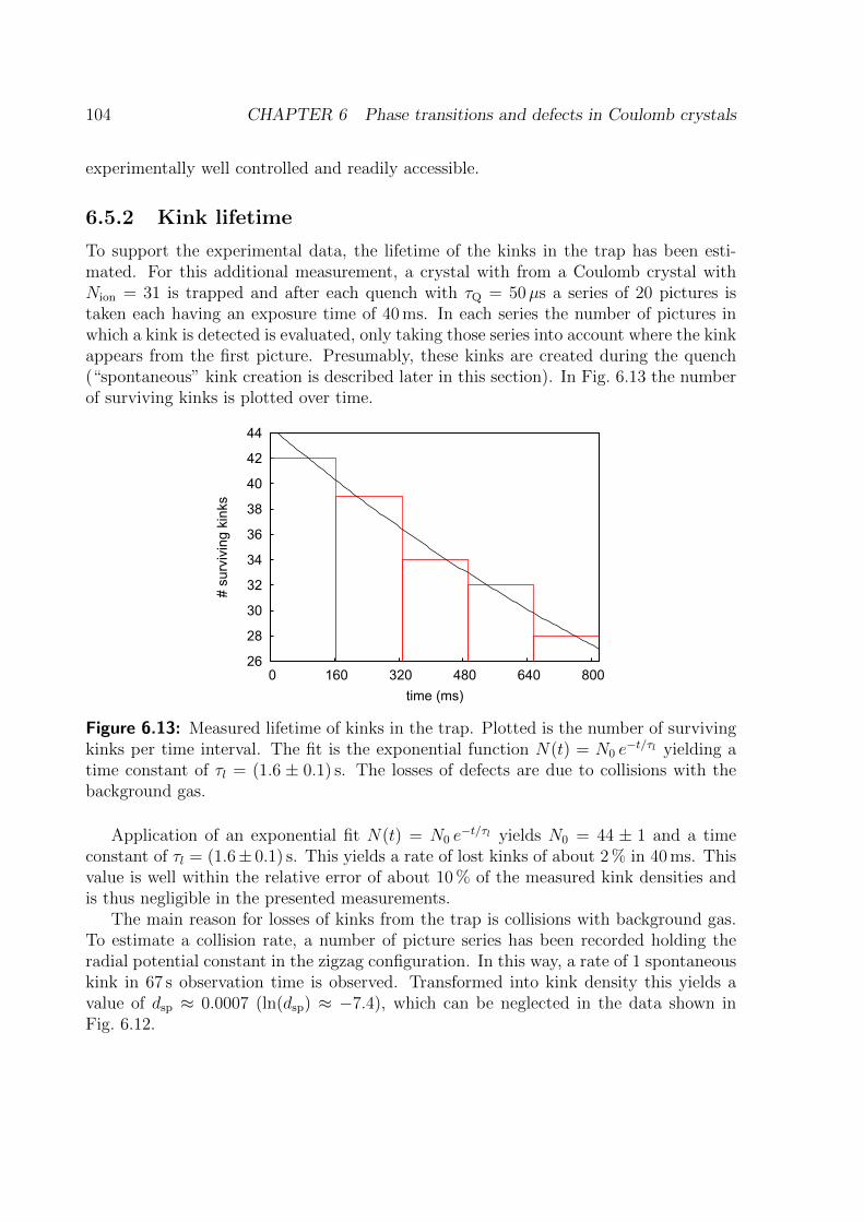
104 CHAPTER 6 Phase transitions and defects in Coulomb crystals
experimentally well controlled and readily accessible.
6.5.2 Kink lifetime
To support the experimental data, the lifetime of the kinks in the trap has been esti-mated. For this additional measurement, a crystal with from a Coulomb crystal withNion = 31 is trapped and after each quench with τQ = 50µs a series of 20 pictures istaken each having an exposure time of 40 ms. In each series the number of pictures inwhich a kink is detected is evaluated, only taking those series into account where the kinkappears from the first picture. Presumably, these kinks are created during the quench(“spontaneous” kink creation is described later in this section). In Fig. 6.13 the numberof surviving kinks is plotted over time.
26
28
30
32
34
36
38
40
42
44
0 160 320 480 640 800
# s
urv
ivin
g k
inks
time (ms)
Figure 6.13: Measured lifetime of kinks in the trap. Plotted is the number of survivingkinks per time interval. The fit is the exponential function N(t) = N0 e
−t/τl yielding atime constant of τl = (1.6 ± 0.1) s. The losses of defects are due to collisions with thebackground gas.
Application of an exponential fit N(t) = N0 e−t/τl yields N0 = 44 ± 1 and a time
constant of τl = (1.6± 0.1) s. This yields a rate of lost kinks of about 2 % in 40 ms. Thisvalue is well within the relative error of about 10 % of the measured kink densities andis thus negligible in the presented measurements.
The main reason for losses of kinks from the trap is collisions with background gas.To estimate a collision rate, a number of picture series has been recorded holding theradial potential constant in the zigzag configuration. In this way, a rate of 1 spontaneouskink in 67 s observation time is observed. Transformed into kink density this yields avalue of dsp ≈ 0.0007 (ln(dsp) ≈ −7.4), which can be neglected in the data shown inFig. 6.12.

Chapter 7
Summary and outlook
In this work, the design of a segmented linear Paul trap was introduced and optimized forthe operation in a multi-ion optical clock. Here, mixed-species Coulomb crystals are usedwith 115In+ as clock ions sympathetically cooled by 172Yb+ ions. The latter is furthermoreused as a test system for the characterization of the trap and the experimental apparatus.
From FEM calculations, an optimized geometry could be derived together with anestimate for the required machining and alignment tolerances. Further estimations weredone to give an upper boundary of tolerable rf phase shifts between separate electrodesthat otherwise lead to non-vanishing rf electric fields and hence excess micromotion.From material considerations for the trap wafers, AlN emerged with the most desirableelectric and thermal properties, as well as the need for elaborate machining processes.For the use in a first prototype Rogers 4350BTM turned out to be readily available withsuitable properties. Two prototype traps could be assembled and put into operation.
The experimental apparatus to test the prototype trap was introduced. Here, the all-diode laser based optical setup for 172Yb+ as the atomic test system may be emphasized.The vacuum system was optimized to easily change the traps, versatile optical accessfor the used lasers and for characterizing trap structures in all dimensions in terms of rffields. The detection scheme was set up for single-photon detection, as well as for spatialresolution of Coulomb crystals. The introduced high-Q helical resonator is designedfor low-power rf feed of the trap and the presented dc control unit for low-noise andhigh-precision control of the ions in terms of micromotion compensation.
RF photon-correlation spectroscopy was implemented as the tool to measure excessmicromotion in the traps and characterize them in terms of residual axial rf fields. Withthe presented setup a sensitivity to micromotion-induced systematic frequency shifts of|(∆ν/ν)mm| ≤ 10−19 could be demonstrated, suitable for the trap characterization withenvisaged residual frequency shifts of less than 10−18 over a large trapping region.
Both prototype traps were successfully set into operation and characterized in termsof excess micromotion. The measured axial fields were found to be in accordance withthe FEM calculations considering machining tolerances of the trap parts. Here, a cleardistinction can be made between the two traps in terms of the used fabrication techniques.The trap with the laser machined parts exhibit a smaller deviation from the calculatedvalues, which assume zero tolerance. In the case of the milled trap, the derivation to
105

106 CHAPTER 7 Summary and outlook
the calculations is about a factor of two larger compared to the laser cut trap, which isaccounted for by the lower precision in machining.
As for the measurements on the linear to zigzag phase transition in 172Yb+ Coulombcrystals, a measurement scheme was demonstrated to investigate scaling laws of therate of defects formed during the phase transition depending on the rate at which thetransition occurs. The obtained results show good agreement to numerical simulations,which were also used to study kink dynamics directly after the phase transition, a regimethat is not accessible with the experiment. The results may give rise to new possibleregimes for the KZM in inhomogeneous systems with finite size. They are supported bythe results of other experiments in similar, as well as different physical systems.
For the measurements regarding KZM scaling in the linear to zigzag phase transition,several scenarios are at hand for the near future.
First, to further support the existing data, measurements could be attempted in theinhomogeneous KZM regime, where the kink density is not limited by a maximum of onedefect per quench, and to directly observe a scaling that is predicted within the KZM.For this to be realized, several aspects need to be considered: reduction of defect lossesfor fast quenches by increasing the friction1, measuring statistics of odd kinks instead ofextended kinks, which easily annihilate due to the shape of the Peierls-Nabarro potential,see Sec. 6.3.3, and increasing the system size in the zigzag region (increase Nion) in orderto reduce interaction between odd kinks.
0
500
1000
1500
2000
2500
# k
inks
left center right
no molecules
molecules
Figure 7.1: Spatial distribution of kinks detected along the crystal. Compared are kinkswhere no molecules are present (light blue) with kinks in the presence of molecules (darkblue). The error bars are calculated assuming a binomial distribution of the number ofkinks. The asymmetry in the number of kinks counted on the left and right end couldbe explained by light-forces that act on the cooled 172Yb+ ions but not on the molecules,thus pushing the ions to the right, which displaces the molecules to the left.
1This is to a certain extent possible by increasing the cooling laser intensity in this experiment. Inanother setup the use of lighter ion species is possible.

107
Second, the inevitable occurrence of molecular ions due to background gas collisionsleads to interesting studies of kink dynamics. For example, a molecule could be thoughtof as a seed for kinks, as a statistical analysis of pictures with Coulomb crystals containingmolecules indicates. Here, the kink density increases for slow quenches compared to thekink densities measured without molecules, as shown in Fig. 6.12.
Furthermore, the fact that the heavier molecules experience a lower rf confinementmay lead to a modification of the Peierls-Nabarro potential, such that a local minimumoccurs at the position of the molecule, thus stabilizing the kink. This behaviour isindicated by the analysis shown in Fig. 7.1. Here, the spatial distribution of the numberof detected kinks is plotted, according to the definition of location given in Fig. 6.11. Thesame data as for the statistical analysis in Ch. 6 are plotted as kinks without molecules(light blue boxes). Data not included in the KZM analysis due to the appearance ofmolecules are plotted as such (dark blue boxes). As the Peierls-Nabarro potential forextended kinks shows a local minimum in the center of the ion crystal the kinks arealmost exclusively detected in the center of the trap, indicating the migration of kinkscreated at the sides of the crystal2. In contrast to that, the kinks that are created whilea molecule is present in the crystal, are nearly equally distributed over the length of thezigzag. First simulations indicate that a molecule rather stops a kink than to act as aseed. Nevertheless, it can alter the kink density depending on the mass of the moleculeand moreover its position in the crystal. As the creation of kinks seems to be suppressedin the center, its probability increases towards the edges of the crystal.
As a future perspective for the acquisitions of this work in terms of the trap devel-opment several points may be named.
Within the current setup, magnetic field measurements may be carried out in allthree trap segments in order to characterize the field distribution within the prototypetrap to evaluate the influence of external stray fields and field gradients, for exampledue to the ion-getter pump and the earth-magnetic field. This is important to give anestimate of the uncertainties depending on inhomogeneous magnetic fields and the sizeof the ion chains.
With compensation of the magnetic fields, detailed spectroscopy of the 2F7/2 ↔1[5/2]5/2 transition of 172Yb+ may be done, in order to provide experimental data on thelevel structure of this theoretically non-trivial transition.
In terms of trap development, the realization of an ion trap based on AlN wafers withfully non-magnetic parts comes within reach, as laser cutting and coating techniques arecurrently optimized. The rigid structure together with low machining tolerances shouldlead to further reduction of axial rf fields due to machining tolerances. Currently underinvestigation is the heat distribution in a Rogers 4305TM model trap. This will help toestimate the uncertainty of frequency shifts due to blackbody radiation and is expectedto be significantly reduced in an AlN based trap.
The first successful loading and trapping of mixed 172Yb+/115In+ Coulomb crystals(see Fig. 7.2) allows for the detailed experimental analysis of the crystal mode structureas a prerequisite to efficient sub-Doppler cooling, which is an inevitable step forward for
2As this should happen on time scales given by the axial trap frequency, this dynamics cannot beresolved with exposure times of tens of milliseconds.

108 CHAPTER 7 Summary and outlook
recoil-free clock spectroscopy. This will be done with the stable laser which is currentlybeing set up to drive the 2D5/2 ↔ 2S1/2 transition.
Mastering these preparatory tasks, paves the way towards versatile quantum sen-sors incorporated by laser cooled Coulomb crystals that can be manipulated in a well-controlled environment. These may find applications in optical frequency standardsbased on many 115In+ ions or precision spectroscopy with unprecedented resolution.Portable systems allow for applications in geodesy and navigation in space on a newlevel.
Figure 7.2: Coulomb crystal with 172Yb+ ions fluorescing at 369 nm and sympatheti-cally cooled 115In+ ions (indicated by white circles). The indium ions are confirmed bymeasuring the mass-dependent secular modes of the crystal via parametric excitation.

Appendix A
DC control schematic
109

110 CHAPTER A DC control schematic
402k
82k5
100k
1M
10R
10k2n7
100p
82k5
100k
1M
2n7
100p
390k 390k
820p 100k
1n8
10k
100n
100n
LF412
LF412
LF412
LF412
390k 390k
22k
100k
10k470p
330p
82k5
100k
1M
10R
10k2n7
100p
100n
100n
LF412
LF412
82k5
100k
1M
(1M
)
10k2n7
100p
82k5
100k
1M
10R
10k2n7
100p
100n
100n
15V
15V
402k
82k5
100k
1M
(1M
)
10k2n7
100p
82k510
0k1M
2n7
100p
390k 390k
820p 100k
1n8
10k
LF412
LF412
LF412
LF412
390k 390k
22k
100k
10k470p
330p
82k5
100k
1M
10R
10k2n7
100p
LF412
LF412
82k5
100k
1M
10R
10k2n7
100p
82k5
100k
1M
10R
10k2n7
100p
100n
100n
100n
100n
100n
100n
100µF 100µF
100µF 100µF
100µH
100µH15V
15V
402k
82k5
100k
1M
10R
10k2n7
100p
82k5
100k
1M
2n7
100p
390k 390k
820p 100k
1n8
10k
LF412
LF412
LF412
LF412
390k 390k
22k
100k
10k470p
330p
82k5
100k
1M
10R
10k2n7
100p
LF412
LF412
82k5
100k
1M
10R
10k2n7
100p
82k5
100k
1M
10R
10k2n7
100p
100n
100n
100n
100n
100n
100n
R1
R2R3
R4
R5
R6C1
C2
R7R8
R9
C3
C4
R10 R11
C5R12
C6
R13
C7
C8
IC1.A3
21
IC1.B5
67
IC1.P
ST1C1C2C3C4C5C6C7C8C9C10C11C12C13C14C15C16C17C18C19C20C21C22C23C24C25C26C27C28C29C30C31C32
A1A2A3A4A5A6A7A8A9
A10A11A12A13A14A15A16A17A18A19A20A21A22A23A24A25A26A27A28A29A30A31A32
3
21IC2.A
IC2.B5
67
IC2.P
R14 R15
R16
R17
R18C9
C10
R19R20
R21
R22
R23C11
C12
C13
C14
IC3.A3
21
IC3.B5
67
IC3.P
R24R25
R26
R27
R28C15
C16
R29R30
R31
R32
R33C17
C18
C19
C20
R34
R35R36
R37
R38
R39C21
C22
R40R41
R42
C23
C24
R43 R44
C25R45
C26
R46
IC4.A3
21
IC4.B5
67
IC4.P
3
21IC5.A
IC5.B5
67
IC5.P
R47 R48
R49
R50
R51C27
C28
R52R53
R54
R55
R56C29
C30
IC6.A3
21
IC6.B5
67
IC6.P
R57R58
R59
R60
R61C31
C32
R62R63
R64
R65
R66C33
C34
C35
C36
C37
C38
C39
C40
C41 C42
C43 C44
L1
L2
R67
R68R69
R70
R71
R72C45
C46
R73R74
R75
C47
C48
R76 R77
C49R78
C50
R79
IC7.A3
21
IC7.B5
67
IC7.P
3
21IC8.A
IC8.B5
67
IC8.P
R80 R81
R82
R83
R84C51
C52
R85R86
R87
R88
R89C53
C54
IC9.A3
21
IC9.B5
67
IC9.P
R90R91
R92
R93
R94C55
C56
R95R96
R97
R98
R99C57
C58
C59
C60
C61
C62
C63
C64
UT1_OUT3
UT2_OUT3
UK1_OUT3
UK2_OUT3
UA1_OUT3
(UA2)_OUT3(UA2)_OUT2
UA1_OUT2
UK2_OUT2
UK1_OUT2
UT2_OUT2
UT1_OUT2UT1_OUT1
UT2_OUT1
UK1_OUT1
UK2_OUT1
UA1_OUT1
(UA2)_OUT1
UAX2_IN3
UAX1_IN3
UC_IN3
UTC_IN3
UT_IN3
UAX2_IN2
UAX1_IN2
UC_IN2
UTC_IN2
UT_IN2
UT_IN1
UTC_IN1
UC_IN1
UAX1_IN1
UAX2_IN1
A
B
C
D
E
1 2 3 4 5 6 7 8
A
B
C
D
E
1 2 3 4 5 6 7 8
4
8
4
8
4
8
4
8
4
8
4
8
Ionenfalle_Analog'10
16.11.2012 13:54:00Bearbeitet am:
Zeichnung:
4.4 PTB
Blatt Nr.: 1/1
4
8
4
8
4
8
Figure A.1: Schematic of the dc control unit.

Bibliography
[1] F. Riehle, Frequency Standards: Basics and Applications. Wiley-VCH, 2004. 7
[2] T. Rosenband et al., “Frequency ratio of Al+ and Hg+ single-ion optical clocks;metrology at the 17th decimal place,” Science, vol. 319, no. 5871, pp. 1808–1812,2008. 7, 12, 13
[3] C. W. Chou, D. B. Hume, T. Rosenband, and D. J. Wineland, “Optical clocks andrelativity,” Science, vol. 329, no. 5999, pp. 1630–1633, 2010. 7
[4] L. Essen and J. V. L. Parry, “An atomic standard of frequency and time interval:A Caesium resonator,” Nature, vol. 176, pp. 280–282, 1955. 8
[5] T. W. Hansch and A. L. Schawlow, “Cooling of gases by laser radiation,” OpticsCommunications, vol. 13, no. 1, pp. 68–69, 1975. 8
[6] D. J. Wineland and H. G. Dehmelt, “Principles of the stored ion calorimeter,”Journal of Applied Physics, vol. 46, no. 2, pp. 919–930, 1975. 8
[7] D. J. Wineland, R. E. Drullinger, and F. L. Walls, “Radiation-pressure cooling ofbound resonant absorbers,” Physical Review Letters, vol. 40, no. 25, pp. 1639–1642,1978. 8
[8] W. Neuhauser, M. Hohenstatt, P. Toschek, and H. Dehmelt, “Visual observationand optical cooling of electrodynamically contained ions,” Applied Physics A:Materials Science & Processing, vol. 17, no. 2, pp. 123–129, 1978. 8
[9] M. A. Kasevich, E. Riis, S. Chu, and R. G. DeVoe, “RF Spectroscopy in an AtomicFountain,” Physical Review Letters, vol. 63, no. 6, pp. 612–615, 1989. 8
[10] A. Clairon, C. Salomon, S. Guellati, and W. D. Phillips, “Ramsey resonance in azacharias fountain,” Europhysics letters, vol. 16, no. 2, pp. 165–170, 1991. 8
[11] W. Neuhauser, M. Hohenstatt, P. E. Toschek, and H. Dehmelt, “Localized visibleBa+ mono-ion oscillator,” Physical Review A, vol. 22, no. 3, p. 1137, 1980. 8
[12] H. G. Dehmelt, “Mono-ion oscillator as potential ultimate laser frequency standard,”in 35th Annual Frequency Control Symposium. 1981. IEEE, 1981, pp. 596–601. 8
111

112 BIBLIOGRAPHY
[13] B. C. Young, F. C. Cruz, W. M. Itano, and J. C. Bergquist, “Visible lasers withsubhertz linewidths,” Physical Review Letters, vol. 82, no. 19, pp. 3799–3802, 1999.8
[14] T. Kessler, C. Hagemann, C. Grebing, T. Legero, U. Sterr, F. Riehle, M. J. Martin,L. Chen, and J. Ye, “A sub-40-mhz-linewidth laser based on a silicon single-crystaloptical cavity,” Nature Photonics, vol. 6, no. 10, pp. 687–692, 2012. 8
[15] D. J. Jones, S. A. Diddams, J. K. Ranka, A. Stentz, R. S. Windeler, J. L. Hall, andS. T. Cundiff, “Carrier-envelope phase control of femtosecond mode-locked lasersand direct optical frequency synthesis,” Science, vol. 288, no. 5466, pp. 635–639,2000. 8
[16] C. W. Chou, D. B. Hume, J. C. J. Koelemeij, D. J. Wineland, and T. Rosenband,“Frequency comparison of two high-accuracy Al+ optical clocks,” Physical ReviewLetters, vol. 104, p. 070802, 2010. 8, 13
[17] P. O. Schmidt, T. Rosenband, C. Langer, W. M. Itano, J. C. Bergquist, and D. J.Wineland, “Spectroscopy Using Quantum Logic,” Science, vol. 309, no. 5735, pp.749–752, 2005. 8, 10
[18] M. Roberts, P. Taylor, G. P. Barwood, P. Gill, H. A. Klein, and W. R. C. Rowley,“Observation of an electric octupole transition in a single ion,” Physical ReviewLetters, vol. 78, pp. 1876–1879, 1997. 8, 44
[19] N. Herschbach, K. Pyka, J. Keller, and T. E. Mehlstaubler, “Linear paul trap designfor an optical clock with coulomb crystals,” Applied Physics B, vol. 107, no. 4, pp.891–906, 2012. 8, 10, 12, 21, 22, 24, 72, 75, 77
[20] C. Champenois, M. Marciante, J. Pedregosa-Gutierrez, M. Houssin, M. Knoop, andM. Kajita, “Ion ring in a linear multipole trap for optical frequency metrology,”Physical Review A, vol. 81, p. 043410, 2010. 8
[21] M. J. Madsen, W. K. Hensinger, D. Stick, J. A. Rabchuk, and C. Monroe, “Planarion trap geometry for microfabrication,” Physical Review B: Lasers and Optics,vol. 78, pp. 639–651, 2004. 9, 16, 30
[22] J. P. Home and A. M. Steane, “Electrode configurations for fast separation oftrapped ions,” Quantum Information & Computation, vol. 6, no. 4, pp. 289–325,2006. 9
[23] D. Stick, W. K. Hensinger, S. Olmschenk, M. J. Madsen, K. Schwab, and C. Monroe,“Ion trap in a semiconductor chip,” Nature Physics, vol. 2, no. 1, pp. 36–39, 2006.9
[24] S. Schulz, U. Poschinger, K. Singer, and F. Schmidt-Kaler, “Optimization of seg-mented linear paul traps and transport of stored particles,” Fortschritte der Physik,vol. 54, pp. 648–665, 2006. 9

BIBLIOGRAPHY 113
[25] W. K. Hensinger, S. Olmschenk, D. Stick, D. Hucul, M. Yeo, M. Acton,L. Deslauriers, J. Rabchuk, and C. Monroe, “T-junction ion trap array fortwo-dimensional ion shuttling, storage and manipulation,” Physical Review Letters,vol. 88, p. 034101, 2006. 9
[26] D. R. Leibrandt et al., “Demonstration of a scalable, multiplexed ion trap forquantum information processing,” arXiv:0904.2599, 2009. 9
[27] U. Tanaka, R. Naka, F. Iwata, T. Ujimaru, K. R. Brown, I. L. Chuang, and S. Urabe,“Design and characterization of a planar trap,” Journal of Physics B: Atomic,Molecular and Optical Physics, vol. 42, no. 15, p. 154006, 2009. 9
[28] C. E. Pearson, D. R. Leibrandt, W. S. Bakr, W. J. Mallard, K. R. Brown, andI. L. Chuang, “Experimental investigation of planar ion traps,” Physical Review A,vol. 73, p. 032307, march 2006. 9
[29] D. T. C. Allcock et al., “Heating rate and electrode charging measurements in ascalable, microfabricated, surface-electrode ion trap,” Applied Physics B, vol. 107,no. 4, pp. 913–919, 2012. 9
[30] Q. A. Turchette et al., “Heating of trapped ions from the quantum ground state,”Physical Review A, vol. 61, no. 6, p. 063418, 2000. 9, 12, 17
[31] N. Daniilidis, S. Narayanan, S. A. Moller, R. Clark, T. E. Lee, P. J. Leek, A. Wallraff,S. Schulz, F. Schmidt-Kaler, and H. Haffner, “Fabrication and Heating Rate Studyof Microscopic Surface Electrode Ion Traps,” New Journal of Physics, vol. 13, no. 1,p. 013032, 2011. 9, 17
[32] E. Peik, G. Hollemann, and H. Walther, “Laser cooling and quantum jumps of asingle indium ion,” Physical Review A, vol. 49, no. 1, p. 402, 1994. 10
[33] T. Liu et al., “Frequency control symposium, 2007 joint with the 21st europeanfrequency and time forum,” in IEEE International, vol. 407, 2007. 10
[34] J. A. Sherman, W. Trimble, S. Metz, W. Nagourney, and N. Fortson, “Progresson indium and barium single ion optical frequency standards,” in LEOS SummerTopical Meetings, 2005 Digest of the. IEEE, 2005, pp. 99–100. 10
[35] C. Schwedes, E. Peik, J. Von Zanthier, A. Y. Nevsky, and H. Walther, “Narrow-bandwidth diode-laser-based blue and ultraviolet light source,” Applied Physics B:Lasers and Optics, vol. 76, no. 2, pp. 143–147, 2003. 10
[36] J. B. Wubbena, S. Amairi, O. Mandel, and P. O. Schmidt, “Sympathetic coolingof mixed-species two-ion crystals for precision spectroscopy,” Physical Review A,vol. 85, p. 043412, 2012. 11
[37] K. Sugiyama and J. Yoda, “Production of YbH+ by chemical reaction of Yb+ inexcited states with H2 gas,” Physical Review A, vol. 55, p. 10, 1997. 11

114 BIBLIOGRAPHY
[38] D. J. Berkeland, J. D. Miller, J. C. Bergquist, W. M. Itano, and D. J. Wineland,“Minimization of ion micromotion in a Paul trap,” Journal of Applied Physics,vol. 83, pp. 5025–5033, 1998. 12, 13, 16, 19, 67, 68
[39] E. Peik, J. Abel, T. Becker, J. Von Zanthier, and H. Walther, “Sideband cooling ofions in radio-frequency traps,” Physical Review A, vol. 60, no. 1, p. 439, 1999. 12
[40] L. Deslauriers, S. Olmschenk, D. Stick, W. K. Hensinger, J. Sterk, and C. Monroe,“Scaling and suppression of anomalous heating in ion traps,” Physical ReviewLetters, vol. 97, no. 10, p. 103007, 2006. 12
[41] R. J. Epstein et al., “Simplified motional heating rate measurements of trappedions,” Physical Review A, vol. 76, no. 3, p. 033411, 2007. 12
[42] M. S. Safronova, M. G. Kozlov, and C. W. Clark, “Precision calculation ofblackbody radiation shifts for optical frequency metrology,” Physical ReviewLetters, vol. 107, p. 143006, 2011. 12, 13
[43] T. Rosenband, W. M. Itano, P. O. Schmidt, D. B. Hume, J. C. J. Koelemeij, J. C.Bergquist, and D. J. Wineland, “Blackbody radiation shift of the 27Al+ 1S0 → 3P0
transition,” in 20th European Frequency and Time Forum (EFTF). IEEE, 2006,pp. 289–292. 12
[44] T. Becker, J. V. Zanthier, A. Y. Nevsky, C. Schwedes, M. N. Skvortsov, H. Walther,and E. Peik, “High-resolution spectroscopy of a single in+ ion: Progress towards anoptical frequency standard,” Physical Review A, vol. 63, no. 5, p. 051802, 2001. 13
[45] J. E. Bernard and A. A. Marmet, L .and Madej, “A laser frequency lock referencedto a single trapped ion,” Optics communications, vol. 150, no. 1, pp. 170–174, 1998.13
[46] F. G. Major, V. N. Gheorghe, and G. Werth, Charged Particle Traps: Physics andTechniques of Charged Particle Field Confinement. Springer, 2004, vol. 37. 13, 17
[47] P. K. Ghosh, Ion Traps. Clarendon Press Oxford, 1995. 13
[48] C. A. Schrama, E. Peik, W. W. Smith, and H. Walther, “Novel Miniature IonTraps,” Optics Communication, vol. 101, pp. 32–36, 1993. 16
[49] K. Smith and R. E. Alley, Electrical Circuits: An Introduction. Cambridge Uni-versity Press, 1992. 20
[50] B. C. Fawcett and M. Wilson, “Computed Oscillator Strengths, and Lande g-Values,and Lifetimes in Yb II,” Atomic Data and Nuclear Data Tables, vol. 47, p. 241, 1991.44, 70
[51] M. M. Schauer, J. R. Danielson, A. T. Nguyen, L. B. Wang, X. Zhao, and J. R.Torgerson, “Collisional population transfer in trapped Yb+ ions,” Physical ReviewA, vol. 79, p. 062705, Jun 2009. 44

BIBLIOGRAPHY 115
[52] D. Das, S. Barthwal, A. Banerjee, and V. Natarajan, “Absolute frequencymeasurements in Yb with 0.08 ppb uncertainty: Isotope shifts and hyperfinestructure in the 399 nm 1S0 →1P1 line,” Physical Review A, vol. 72, p. 032506,2005. 51
[53] Y. H. Wang, T. Liu, R. Dumke, A. Stejskal, Y. N. Zhao, J. Zhang, Z. H. Lu,L. J. Wang, T. Becker, and H. Walther, “Improved absolute frequency measurementof the 115In+ 5s2 1S0-5s5p 3P0 narrowline transition: Progress towards an opticalfrequency standard,” Laser physics, vol. 17, no. 7, pp. 1017–1024, 2007. 52
[54] W. W. Macalpine and R. O. Schildknecht, “Coaxial Resonators with Helical InnerConductor,” in Proceedings of the Institute of Radio Engineers, 1959, p. 2099. 53
[55] P. D. Lett, W. D. Phillips, S. L. Rolston, C. E. Tanner, R. N. Watts, and C. I.Westbrook, “Optical molasses,” Journal of the Optical Society of America B, vol. 6,no. 11, pp. 2084–2107, 1989. 63
[56] E. Peik, “Laserspektroskopie an gespeicherten In-Ionen,” Ph.D. dissertation, Max-Planck-Institut fur Quantenoptik, 1993. 69
[57] K. Pyka et al., “Symmetry breaking and topological defect formation in ioncoulomb crystals,” arXiv:1211.7005, 2012. 87
[58] T. W. B. Kibble, “Topology of cosmic domains and strings,” Journal of Physics A:Mathematical and General, vol. 9, p. 1387, 1976. 88
[59] T. W. B. Kibble, “Some implications of a cosmological phase transition,” PhysicsReports, vol. 67, no. 1, pp. 183–199, 1980. 88
[60] W. H. Zurek, “Cosmological experiments in superfluid helium?” Nature, vol. 317,no. 6037, pp. 505–508, 1985. 88
[61] W. H. Zurek, “Cosmological experiments in condensed matter systems,” PhysicsReports, vol. 276, no. 4, pp. 177–221, 1996. 88
[62] S. M. Griffin, M. Lilienblum, K. Delaney, Y. Kumagai, M. Fiebig, and N. A.Spaldin, “From multiferroics to cosmology: Scaling behaviour and beyond in thehexagonal manganites,” arXiv:1204.3785, 2012. 88
[63] I. Chuang, R. Durrer, N. Turok, and B. Yurke, “Cosmology in the laboratory:Defect dynamics in liquid crystals,” Science, vol. 251, no. 4999, pp. 1336–1342,1991. 88
[64] M. J. Bowick, L. Chandar, E. A. Schiff, and A. Srivastava, “The Cosmological KibbleMechanism in The Laboratory: String Formation in Liquid Crystals,” Science, vol.263, no. 5149, pp. 943–945, 1994. 88

116 BIBLIOGRAPHY
[65] R. Monaco, J. Mygind, M. Aarøe, R. Rivers, and V. Koshelets, “Zurek-KibbleMechanism for The Spontaneous Vortex Formation in Nb-Al/Al-ox/Nb JosephsonTunnel Junctions: New Theory and Experiment,” Physical Review Letters, vol. 96,no. 18, 2006. 88
[66] L. E. Sadler, J. M. Higbie, S. R. Leslie, M. Vengalattore, and D. M. Stamper-Kurn,“Spontaneous symmetry breaking in a quenched ferromagnetic spinor Bose-Einsteincondensate,” Nature, vol. 443, no. 7109, pp. 312–315, 2006. 88
[67] C. N. Weiler, T. W. Neely, D. R. Scherer, A. S. Bradley, M. J. Davis, and B. P.Anderson, “Spontaneous vortices in the formation of Bose-Einstein condensates,”Nature, vol. 455, no. 7215, pp. 948–951, 2008. 88
[68] E. M. Lifshitz and L. P. Pitaevskii, “Landau and Lifshitz Course of TheoreticalPhysics. Statistical Physics, Vol. 5,” 1980. 88
[69] V. L. Ginzburg and L. D. Landau, “On the theory of superconductivity,” in OnSuperconductivity and Superfluidity. Springer, 2009, pp. 113–137. 88
[70] B. Damski and W. H. Zurek, “Soliton creation during a Bose-EinsteinCondensation,” Physical Review Letters, vol. 104, p. 160404, 2010. 88
[71] A. del Campo, G. De Chiara, G. Morigi, M. B. Plenio, and A. Retzker, “Structuraldefects in ion chains by quenching the external potential: The inhomogeneousKibble-Zurek mechanism,” Physical Review Letters, vol. 105, no. 7, p. 075701,2010. 88, 89, 90, 103
[72] H. Saito, Y. Kawaguchi, and M. Ueda, “Kibble-Zurek mechanism in a quenchedferromagnetic Bose-Einstein condensate,” Physical Review A, vol. 76, no. 4, 2007.88, 92
[73] R. Monaco, J. Mygind, and R. J. Rivers, “Zurek-Kibble domain structures: Thedynamics of spontaneous vortex formation in annular Josephson tunnel junctions,”Physical Review Letters, vol. 89, no. 8, 2002. 88
[74] R. Monaco, J. Mygind, R. Rivers, and V. Koshelets, “Spontaneous fluxoidformation in superconducting loops,” Physical Review B, vol. 80, no. 18, 2009. 88,89, 92
[75] W. H. Zurek, “Causality in condensates: Gray solitons as relics of BEC formation,”Physical Review Letters, vol. 102, no. 10, 2009. 89
[76] G. D. Chiara, A. d. Campo, G. Morigi, M. B. Plenio, and A. Retzker, “Spontaneousnucleation of structural defects in inhomogeneous ion chains,” New Journal ofPhysics, vol. 12, no. 11, p. 115003, 2010. 89, 91, 94

BIBLIOGRAPHY 117
[77] J. Sabbatini, W. H. Zurek, and M. J. Davis, “Causality and defect formationin the dynamics of an engineered quantum phase transition in a coupled binaryBose-Einstein condensate,” New Journal of Physics, vol. 14, no. 9, p. 095030, 2012.89
[78] A. Retzker, R. Thompson, D. Segal, and M. Plenio, “Double well potentials andquantum phase transitions in ion traps,” Physical Review Letters, vol. 101, no. 26,2008. 90
[79] S. Fishman, G. De Chiara, T. Calarco, and G. Morigi, “Structural phase transitionsin low-dimensional ion crystals,” Physical Review B, vol. 77, no. 6, p. 064111, 2008.90
[80] A. Steane, “The ion trap quantum information processor,” Applied Physics B:Lasers and Optics, vol. 64, no. 6, pp. 623–643, 1997. 90
[81] D. H. E. Dubin, “Theory of structural phase transitions in a trapped Coulombcrystal,” Physical Review Letters, vol. 71, no. 17, pp. 2753–2756, 1993. 90
[82] P. Laguna and W. H. Zurek, “Critical dynamics of symmetry breaking: Quenches,dissipation, and cosmology,” Physical Review D, vol. 58, no. 8, p. 085021, 1998. 91
[83] H. J. Metcalf and P. Van der Straten, Laser Cooling and Trapping. Springer Verlag,1999. 91
[84] A. del Campo, A. Retzker, and M. B. Plenio, “The inhomogeneous Kibble-Zurekmechanism: Vortex nucleation during Bose-Einstein condensation,” New Journalof Physics, vol. 13, no. 8, p. 083022, 2011. 91
[85] J. Dziarmaga, “Dynamics of a quantum phase transition and relaxation to a steadystate,” Advances in Physics, vol. 59, no. 6, pp. 1063–1189, 2010. 92
[86] H. Landa, S. Marcovitch, A. Retzker, M. B. Plenio, and B. Reznik, “Quantumcoherence of discrete kink solitons in ion traps,” Physical Review Letters, vol. 104,no. 4, p. 043004, 2010. 92
[87] K. Kuhlmann, “Untersuchung des Inhomogenen Kibble-Zurek-Mechanismus in172Yb+-Coulomb-Kristallen,” Master’s thesis, Technische Universitat Braunschweig,2012. 92
[88] D. M. Meier, “Ein Lasersystem zur Seitenbandspektroskopie von gemischtenIn+/Yb+ Kristallen,” Master’s thesis, Technische Universitat Braunschweig, 2012.93, 94
[89] O. M. Braun and Y. S. Kivshar, The Frenkel-Kontorova Model: Concepts, Methods,and Applications. Springer Verlag, 2004. 95

118 BIBLIOGRAPHY

Acknowledgments
At this point, I would like to thank all the people that helped me with this work. And Ihave to apologize, because I am not a sentimental guy, so please be assured that I reallymean it when I say thank you.
First of all, there is Dr. Tanja E. Mehlstaubler who gave me the chance of beingpart of this project and always gave me the right push when I thought I didn’t needit, although I did. It was particularly fun to see the empty lab getting filled up withtechnology and people and to see things working for the first time. Being the first in anempty lab is awesome and awful at the same time, but mostly awesome. Especially nowthat everything is running.
Second, I would like to thank Prof. Piet O. Schmidt, Prof. Christian Ospelkaus andProf. Louis Santos for agreeing to referee this manuscript. I really appreciate it.
A particular thank you goes to all the people of the time and frequency divisionfor sharing their experience and resources. Dr. Ekkehard Peik for his helpful adviceand support. Martina Baumler for helping me through the administrative procedures inthe PTB. Hans-Albert Kremling, Thomas Leder and Sven Krenauer for their mechanicalsupport and Burghard Lippert, Andreas Hoppmann and Michael Kazda for the electronicsupport.
A very special thanks goes to Norbert Herschbach, who has a lot of experience andan explanation for everything. It was a pleasure to set up everything with him. JonasKeller is a great colleague to work with and to order pizza at night, and to correct myenglish from time to time. Many thanks goes to Lin Yi, who contributed a lot to theexperiment in his short period in our group. It was a pleasure to work with you.
A special thanks goes to the rest of the Quest team, for a nice atmosphere in the office,for fruitful discussions about physics and everything else, for the pleasant group tripsand christmas parties and more. Borge Hemmerling, Jannes Wubbena, Olaf Mandel,Florian Gebert, Yong Wan, Nils Scharnhorst, it was a pleasure. Sandra Ludwig gavegreat administrative support. Peter-Christian Carstens for his electronic support, as wellas Christopher Bleuel and Olga Lick. Sven Klitzing and Alexander Pablocki for theirmechanical support. Sven and Borge shared their appreciation of a good coffee, this iswhat Premium-usership is really about. It was a pleasure to give advice and share thelab with Kristijan Kuhlmann and David-Marcel Meier, as well as the monday night sneakpeek. I also would like to thank my new colleagues, that will take over the experimenttogether with Jonas, Tobias Burgermeister and Heather Partner, who helped a lot inputting this thesis in a better shape. Thanks also for contributing that much to thepaper. I will particularly miss the nights in the Roots sports bar to play billiards withNorbert, Jonas and Sven and sometimes Jannes.
The most thanks I have to give to my family for being the constant and groundin my life. At last, because I cannot express how important she is, I thank my wifeSana (thanks again Piet for hiring her) for always believing in me, for supporting me inparticular in the final period of writing and for being this wonderful person. I hope Ican give you half as much support, when it’s your turn.
úæ.JJ.
k
IK@ ½J. m
'


Curriculum vitae
Karsten Pyka
Contact information:[email protected]
Personal informationDate of birth: 17.01.1983Place of birth: Robel/MuritzNationality: German
Education
03/2009-04/2013 Physikalisch-Technische Bundesanstalt, Leibniz Univer-sitat Hannover, GermanyGraduate student in the group of Dr. Tanja E. Mehlstaubler atthe QUEST institute for experimental quantum metrology and atthe time and frequency divisionThesis topic: High-precision ion trap for a multi-ion optical clock
10/2003-09/2008 University of Hamburg, GermanyDiploma student in the group of Prof. Klaus Sengstock at theInstitute for laser physicsDiploma thesis title: Bragg-spectroscopy of degenerate quantumgases in optical lattices
06/2002 Joliot-Curie Gymnasium, GermanyAbitur

List of publications
1. K. Pyka et al. Symmetry Braking and Topological Defect Formation in Ion CoulombCrystals. arXiv:1211.7005, 2012.
2. K. Pyka, N. Herschbach, J. Keller and T. E. Mehlstaubler. A high-precision rftrap with minimized micromotion for an In+ multiple-ion clock. arXiv:1206.5111,2012.
3. N. Herschbach, K. Pyka, J. Keller and T. E. Mehlstaubler. Linear Paul trap designfor an optical clock with Coulomb crystals. Applied Physics B: Lasers and Optics,vol. 107, pp. 891–906, 2011.
4. P. T. Ernst, S. Gotze, J. S. Krauser, K. Pyka, D.-S. Luhmann, D. Pfannkuche andK. Sengstock. Probing superfluids in optical lattices by momentum-resolved Braggspectroscopy. Nature Physics, vol. 6, 2010.