high performance and traditional multicrystalline silicon ...oa.upm.es/39903/11/hpmc-si_mc-si...
TRANSCRIPT

1
Digital Object Identifier: 10.1109/JPHOTOV.2016.2540246
Abstract—In recent years, high-performance multicrystalline silicon (HPMC-Si) has emerged as an attractive alternative to traditional ingot-based multicrystalline silicon (mc-Si), with a similar cost structure but improved cell performance. Herein, we evaluate the gettering response of traditional and high-performance multicrystalline silicon. Microanalytical techniques demonstrate that HPMC-Si and mc-Si share similar lifetime-limiting defect types, but have different relative concentrations and distributions. HPMC-Si shows a substantial lifetime improvement after P-gettering compared to mc-Si, chiefly because of lower area fraction of dislocation-rich clusters. In both materials, the dislocation clusters and grain boundaries were associated with relatively higher interstitial iron point defect concentrations after diffusion, suggestive of dissolving metal-impurity precipitates. The relatively fewer dislocation clusters in HPMC-Si are shown to exhibit similar characteristics to those found in mc-Si. Given similar governing principles, a proxy to determine relative recombination activity of dislocation clusters developed for mc-Si is successfully transferred to HPMC-Si. The lifetime in the remainder of HPMC-Si material is found to be limited by grain-boundary recombination. To reduce the recombination activity of grain boundaries in HPMC-Si, coordinated impurity control during growth, gettering, and passivation must be developed.
Index Terms—defects, dislocations, dislocation recombination activity, eccentricity variation, high-performance multicrystalline silicon, minority-carrier lifetime, photovoltaics, recombination, synchrotron.
S. Castellanos, M. A. Jensen, A. E. Morishige, J. Hofstetter, P. Yen, and T. Buonassisi are with the Massachusetts Institute of Technology, Cambridge, MA 02139 USA (e-mail: [email protected]; [email protected]; aemorish@ mit.edu; [email protected]; [email protected]; [email protected]).
K. E. Ekstrøm and A. Autruffe are with the Department of Materials Science and Engineering, Norwegian University of Science and Technology 7491 Trondheim, Norway (e-mail: [email protected]; antoine.autruffe@ material.ntnu.no).
B. Lai is with the Advanced Photon Source, Argonne National Laboratory, Argonne, IL 60439 USA (e-mail: [email protected]).
G. Stokkan is with the Materials and Chemistry Sector for Sustainable Energy Technology, SINTEF, 7465 Trondheim, Norway (e-mail: Gaute.Stokkan@ sintef.no).
C. del Can ̃izo is with the Instituto de Energıa Solar, Universidad Politecnica de Madrid, 28040 Madrid, Spain (e-mail: [email protected]).
High-Performance and Traditional Multicrystalline Silicon: Comparing Gettering Responses and Lifetime-Limiting Defects
Sergio Castellanos, Kai E. Ekstrøm, Antoine Autruffe, Mallory A. Jensen, Ashley E. Morishige, Jasmin Hofstetter, Patricia Yen, Barry Lai, Gaute Stokkan, Carlos del Cañizo, Tonio Buonassisi
2
I. INTRODUCTION Given the recent downward price trend for photovoltaic (PV) modules, industry is pressed to reduce costs to improve profitability. Increasing module efficiency is an effective approach to system cost reduction
[1, 2]. Because module efficiency is governed in part by wafer quality, industry efforts are focused on reducing wafer defect density while retaining low cost-per-area [3]. In particular, much attention is focused on reducing the density of dislocations, i.e., one-dimensional extended defects, which are among the most detrimental defects in ingot-based multicrystalline silicon (mc-Si) [4-6].
The properties of dislocations have been studied in model structures, such as organized Si/SiGe misfit dislocation arrays [7-9], as well as in industrial multicrystalline silicon [10, 11]. The recombination activity of dislocations has been associated with the decoration of transition metal impurities [12]. A lower dislocation density reduces the number of energetically favorable heterogeneous nucleation sites for metal impurities [13]. During subsequent process steps including phosphorus diffusion gettering and hydrogenation, larger bulk minority-carrier lifetime improvements are observed in silicon with lower dislocation densities [14-19], substantiating the strong empirical link [19-21] between the presence of dislocations and final device performance.
Recent works have detailed the growth methods and structural characteristics of an emerging material referred to as high-performance multicrystalline silicon (HPMC-Si), which has higher quality than mc-Si [22-24]. In contrast to mc-Si, HPMC-Si is known for a lower average grain size and a lower dislocation cluster density due to controlled grain-growth kinetics that render grain boundary (GB) types favorable to a low density of dislocation clusters [25]. However, some dislocation clusters are still present in HPMC-Si.
Because defects, in particular dislocations, can result in an inhomogeneous electrical response after phosphorous diffusion gettering (P-gettering) [13, 18, 19] it is unclear how HPMC-Si responds to P-gettering and how this response compares to P-gettered mc-Si grown under similar conditions. Understanding this response is essential to maximizing the wafer and cell performance, and to guiding future crystal growth developments. Herein, we study both mc-Si and HPMC-Si materials grown under identical growth conditions (e.g., furnace, crucible, crucible lining materials, and feedstock). Samples are selected for processing and analysis at equal ingot heights to elucidate the differences between their dislocation densities and electrical performances upon P-gettering. We compare and quantify the lifetime improvements of both materials after processing. We correlate local differences in regions of low performance with structural and elemental origins (e.g., dislocations and impurities) to assess the root cause(s) of performance differences between mc-Si and HPMC-Si. We also test and validate a methodology in HPMC-Si, previously proposed in mc-Si material [26], which can help determine the relative electrical recombination activity of dislocation clusters in a rapid manner.
II. MATERIALS AND METHODS A. Material Growth
To enable comparison on the basis of material properties, HPMC-Si and mc-Si ingots are prepared using the same polysilicon feedstock, growth furnace, crucible, and crucible lining material. Two p-type boron-doped 12 kg pilot-scale ingots, a seed-assisted HPMC-Si ingot and a conventional mc-Si reference ingot, are grown in a Crystalox DS 250 directional solidification furnace. The crucible used for both materials is a Fused Silica Solar Crucible from Vesuvius coated with Si3N4 from UBE America, containing approximately 29 ppmw and 10 ppmw of Fe, respectively.
The mc-Si ingot is grown from polysilicon chips with 6N purity with a final ingot diameter of 250 mm and height of 105 mm. Melting is performed over a time span of 420 min at a plateau temperature on the susceptor of 1535 °C (actual temperature in the crucible is lower). The cooling process is split into two
3
parts; the first part has a cooling rate of 0.75 °C/min for 70 min, while the second part has a cooling rate of 0.1 °C/min for 400 min, until complete solidification is achieved.
The section of HPMC-Si ingot studied herein is grown also from polysilicon chips, and in the same crucible as the mc-Si ingot. The time-temperature profile differs from that of the mc-Si ingot in that the melting step is shortened in order to prevent complete melting of the polysilicon feedstock (i.e., leaving a residual seed-layer of polysilicon chips on the bottom of the crucible). Melting is performed at the same susceptor temperature of 1535 °C but over a total time span of 170 min, with a split cooling rate of 0.75 °C/min the first 80 min and a cooling rate of 0.1 °C/min for the remaining 360 min. The final ingot is cut into nine 50 × 50 × 105 mm3 bricks, and the three bricks in the central row are wafered by a slurry-based wire-saw.
The circular crucible is cut into nine 50×50×105 mm blocks, and the central row of blocks is then wafered by wire saw. Sample wafers are extracted and laser cut (50 mm × 50 mm × 200 µm) from the same solidified fraction height (f = 0.75) from both mc-Si and HPMC-Si grown bricks, with measured resistivity values of 0.97 Ω-cm and 0.92 Ω-cm, respectively. Samples are selected from central regions away from crucible walls to minimize spurious effects arising from ingot-crucible interactions (e.g. red zone). Statistical measurements across different heights and positions are not performed for this study.
B. Minority-Carrier Lifetime Analysis To conduct minority-carrier lifetime analysis, samples are first saw-damage etched in a
HNO3:CH3COOH:HF volumetric ratio mixture of 36:12:5 for five minutes, which removes approximately 20 µm from the wafer. Samples are then cleaned in an RCA solution to eliminate organic and metal contaminants prior to surface passivation. Surface passivation is performed by first depositing 20 nm of Al2O3 via atomic layer deposition in a Cambridge NanoTech Savannah 200 tool at a temperature of 200 °C, then subsequently annealing the samples at 350 °C for ten minutes in a N2 environment.
Lifetime is mapped with a Semilab WT-2000 microwave-photoconductance decay (µ-PCD) tool with a pixel resolution of 250 µm, both for the as-grown state and after phosphorus diffusion. Normalized “lifetime ratio” maps, slightly similar to those reported in [27], are produced by matching spatial coordinates between the as-grown and P-gettered lifetime maps, and dividing their pixel (lifetime) values. The µ-PCD lifetime values are obtained by fitting a single time constant to a decay curve. Carrier generation rates derived from µ-PCD technique (905 nm laser, 300 K temperature, 180 µm sample thickness, 1×10⁻² cm2 excitation area) are in the order of 1×10¹⁶ carriers/cm3/s. Given the low generation rate from the µ-PCD technique and the correlation with lifetime values measured by calibrated photoluminescence at low injection, we note that µ-PCD lifetime maps are low-injection lifetime values dominated by Shockley-Read-Hall recombination.
Photoluminescence imaging (PLI) is performed with a pixel resolution of approximately 50 µm at a power density of 0.0150 W/m2. PLI is acquired by illuminating passivated samples with a 25 W, 808 nm, fiber-coupled diode laser, and captured with a PIXIS 1024BR Si CCD camera with an InP wafer and a Schott RG1000 long-pass filter to improve sensitivity.
Interstitial iron concentration (Fei) is calculated by measuring lifetime after dissociating iron-boron (Fei-Bs) pairs, and then allowing for re-association for 150 min in the dark, then measuring lifetime again by quasi steady-state photoconductance (QSSPC) (Sinton WCT-120) [28, 29]. The calculation and experimental parameters used herein are detailed in [30]. Noise analysis for the Fei-Bs measurement technique is based on the analysis for the Cri-Bs measurement technique described in [31].
Qualitative, spatially-resolved interstitial iron concentration (i.e., [Fei]) maps are acquired with the PLI experimental setup (laser and camera). The maps are acquired after dissociating Fei-Bs pairs with the diode laser and allowing for pair re-association.
The impact of grain boundaries and grain size upon P-gettering and its combined effect with intragranular

4
dislocation clusters is assessed on the HPMC-Si P-gettered sample by performing line scans between GBs on a PL image. PLI values are normalized from 0 to 1, with a pixel resolution of approximately 50 µm.
C. Phosphorous Diffusion Gettering Wafers are cleaned prior to gettering using an RCA clean. Phosphorous gettering is performed in a Tystar
Tytan 2800 POCl3 furnace, using a time-temperature profile that consists of loading the sample at 700 °C, ramping up to 845 °C, and holding for 30 min before cooling down at a rate of 4.5 °C/min and unloading at 750 °C.
After phosphorous gettering, the samples are etched again in a HNO3:CH3COOH:HF solution (volumetric ratio mixture of 36:12:5) for two minutes removing 8 µm in total and the entire formed emitter, cleaned in RCA, and surface-passivated with Al2O3 for characterization of the materials’ lifetime-performance response to the P-gettering process, with the same lifetime analysis procedure detailed before.
D. Defect Elucidation and Eccentricity Characterization Samples are etched with a Sopori solution (HNO3:CH3COOH:HF with a volumetric ratio of 36:15:1) [32]
for 45 s followed by a room-temperature dilute KOH quench described in [33] to reveal dislocations intersecting the sample surface as etch pits, averaging 6 µm in diameter. Dislocation etch pits are imaged with a Nikon LV 100 optical microscope at a pixel resolution of 1.46 µm.
A previous study associated dislocation recombination activity with the variance of dislocation etch-pit eccentricity [26]. To quantify the variance of dislocation etch-pit eccentricity, two regions on the HPMC-Si samples are analyzed at a higher pixel resolution of 0.15 µm. From the existing dislocation etch pits in these regions, eccentricity values of the etch pits are computed by fitting the pit major and minor axes, as detailed in [26].
E. Metal-Decoration Analysis To identify the presence of metals decorating dislocation clusters, synchrotron-based micro X-Ray
Fluorescence (µ-XRF) measurements are performed at Beamline 2-ID-D at the Advanced Photon Source at Argonne National Laboratory with 10 keV X-ray energy and a 200 nm full-width at half-maximum beam spot size. The selected dislocation etch pits from two different dislocation clusters are scanned via a flyscan method, with a 220 nm step size and a 900 ms dwell time per spot.
III. RESULTS Fig. 1a shows the change in mc-Si minority-carrier lifetime after P-gettering (66-Ω/☐). The first two µ-
PCD maps show the as-grown and P-gettered lifetimes, using the same scale corresponding to lifetime values up to 100 µs. The third frame shows the ratio of P-gettered to as-grown lifetime maps. Lifetime values (i.e., pixels) that did not change after P-gettering have a numerical value of 1. Areas that perform worse after gettering are shown in red, and lighter shades of gray color indicate greater lifetime improvement after P-gettering.
To quantify the differences observed in the lifetime ratio map, the values from both as-grown and P-gettered mc-Si lifetime maps are plotted on the x-axis and y-axis, respectively, of Fig. 1c. The lifetime performance evolution of the mc-Si sample from as-grown and after P-gettering is represented in orange circles. The median lifetime values are binned in 5 µs intervals and shown as yellow triangles. Lifetime performance evolution of HPMC-Si is also shown in gray circles in the background, with their median lifetime values acquired in 5 µs intervals and shown as white squares.

5
Shown in the same scatter plot are three lines with different slopes denoting: no difference in lifetime between the as-grown and P-gettered state (“1:1”), 50% lifetime improvement by P-gettering (“1.5:1”), and 100% improvement after P-gettering (“2:1”). Two arrows show the tendency of lifetime performance after gettering, with directions towards “Better” (above 1:1 slope line), or “Worse” (below 1:1 slope line) regions. The majority of median values for mc-Si lie below the 1:1 dashed line, indicating a decrease in lifetime after P-gettering. Only median values between ~50 µs and ~60 µs in the as-grown state improved.
Fig. 1b shows two µ-PCD lifetime maps of the as-grown and P-gettered HPMC-Si sample (59-Ω/☐), with the third image corresponding to a ratio between P-gettered and as-grown maps. Color-code and values represent the same performance changes as in Fig. 1a. Lifetime values are normalized to the same color bar, corresponding to lifetime values up to 250 µs.
In Fig. 1d, the lifetime values from both HPMC-Si as-grown and P-gettered lifetime maps are plotted on the x-axis and y-axis, respectively. The lifetime performance evolution of the HPMC-SI sample, as-grown and after P-gettering, is represented in green circles, with median lifetime values binned in 5 µs intervals shown as blue squares. Lifetime performance evolution of mc-Si (shown in orange color in Fig. 1c) is also plotted in gray circles in the background, with respective median lifetime values shown as white triangles.
Lines with different improvement intensity slopes are also shown. The majority of median values for HPMC-Si lie above the 1:1 dashed line, and in some instances, close to 2:1. An increased performance is observed in low as-grown lifetime regions (~0 to 50 µs), and in higher as-grown lifetime regions (~60 to100 µs).
Lifetime ratio maps for both mc-Si (Fig. 2a) and HPMC-Si (Fig. 2c) are shown with corresponding [Fei] maps in Fig. 2b and 2d, respectively. Both ratio maps and [Fei] maps (acquired after P-gettering) have a yellow-dashed line enclosing a representative region of interest.
Dislocation etch pit maps from the yellow regions in the mc-Si and HPMC-Si samples are shown in Figs. 2e and 2f, respectively. A higher area fraction of densely clustered dislocation etch pits is observed in the mc-Si sample than the HPMC-Si sample. The red (underperforming) areas correspond to regions with dense dislocation clusters in both samples.
Likewise, the underperforming (red) areas also coincide with higher [Fei] values. Quantitative iron-boron (Fe-B) pair dissociation measurements indicate an average as-grown [Fei] concentration of 1.3×1011 cm-3 in an adjacent mc-Si sample. After a standard P-gettering process, the [Fei] is reduced to 1.1×1010 cm-3. The as-grown [Fei] in the HPMC-Si sample is reduced by 95% from 1.1×1011 cm-3 to 5.4×109 cm-3 upon P-gettering.
A photoluminescence (PL) image of a HPMC-Si region is shown in Fig. 3a. Dark regions represent low counts and low lifetime, while bright regions indicate higher counts and relatively higher lifetime. The PL image corresponds to a region of the HPMC-Si sample that contains dislocation etch pits, as observed in Fig. 3b. Dislocation populations 5.6 mm apart are selected from regions with high PL counts (white square on the left) and low PL counts (white square on the right).
The areas enclosed in the white squares are surveyed for etch-pit eccentricity analysis. Optical micrographs of the two surveyed areas, visibly located in different grains, are shown in Fig. 3c, where the high PL counts region corresponds to the dislocation etch pits shown on the left, and the low PL counts region corresponds to the dislocation etch pits shown on the right.
Frequency histograms of etch-pit eccentricity for each of the dislocation populations are shown in Fig. 3d. These histograms demonstrate the total fraction of dislocation etch pits measured with a given eccentricity value, ranging from 0 (perfect circle) to 1 (elongated ellipse). The eccentricity distribution for the population labeled “Low Recombination” (high PLI counts) is narrower than the distribution for the population labeled “High Recombination” (low PLI counts) in Fig. 3d.
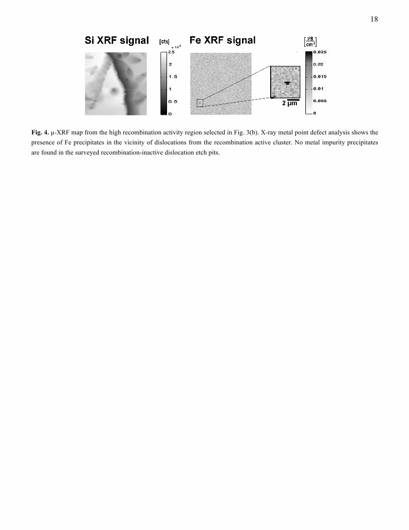
Regions around the enclosed area in white in Fig. 3b are further surveyed with µ-XRF analysis to determine the presence of metal decoration. A total surface area of 912 µm2 and a total surface area of 606

6
µm2 are scanned from the high- and low-recombination activity regions, respectively. The µ-XRF map from the high-recombination activity region is shown in Fig. 4. Different elements are measured; however, given the relatively high detection of Fe fluorescence compared to other elements and its known detrimental impact on solar cell performance, only Si and Fe maps are shown. Dark regions in the Si channel are dislocation etch pits, and dark regions in the Fe channel correspond to a higher count rate of Fe-Kα radiation, indicating the presence of Fe-rich particles. A magnified map within the recombination-active region reveals the presence of Fe-rich particles with an area density of up to 0.037 µg/cm2. There is no signal above the noise floor of 0.010 µg/cm2 detected in the Fe channel for the five recombination-inactive dislocation etch pits surveyed (not shown).
To determine the combined effect of intragranular dense dislocation clusters with GBs — the latter being present in relatively higher density in HPMC-Si — a minority carrier lifetime analysis is performed in the P-gettered HPMC-Si sample across different grains, with and without dense dislocation clusters.
A PL image of the HPMC-Si P-gettered sample is shown in Fig. 5a. Dark regions represent low PL counts and relate to low minority-carrier lifetimes, while bright regions indicate high counts and relatively higher lifetimes. The influence of grain boundaries in minority-carrier lifetime is analyzed by performing a linescan analysis between two grains and across a grain boundary, shown by a red line in Fig. 5b, where the normalized minority-carrier lifetime variation is shown as a function of distance from the grain boundary. The maximum normalized PLI count is acquired at the center of 65 different grains, indicating their relative intragranular carrier lifetime, and plotted on the y-axis of Fig. 5c. On the x-axis, the distance measured between GBs through their minor axes (conservative proxy for grain size) is plotted. The open circles correspond to grains without dense intragranular dislocation clusters, and red rhomboids correspond to grains with high densities of intragranular dislocations.
IV. DISCUSSION A striking electronic-quality difference between HPMC-Si and mc-Si is their response to P-gettering. A
much larger lifetime improvement is observed after gettering of HPMC-Si than mc-Si, as quantified in Fig. 1. For HPMC-Si, 75% of the analyzed wafer area in Fig. 1 improve after gettering, i.e., have a “lifetime ratio” (final divided by initial lifetimes) greater than one. In contrast, for mc-Si, only 49% of the lifetime values improve upon gettering (i.e., found above the 1:1 ratio line in Fig. 1c.). Although the authors expect the electronic-quality differences found in these samples to be representative of these multicrystalline silicon materials, a larger statistical sampling is required (and not undertaken herein) to generalize such differences.
To assess the root cause(s) of the difference in performance improvement with gettering, microanalytical techniques are employed. Our results show that HPMC-Si and mc-Si share similar lifetime-limiting defect types, yet the relative concentrations and distributions are different. Compared to traditional mc-Si, HPMC-Si contains a smaller area-fraction affected by high dislocation density; those remaining dislocations in HPMC-Si nevertheless exhibit similar characteristics to those in mc-Si. Furthermore, the grain boundaries of HPMC-Si are recombination active, and the recombination activity thereof must be reduced (e.g., through impurity control during growth, gettering, and passivation) to enable high-performance devices.
A. Dislocated Area Fraction Governs Gettering Response Regions of high dislocation density in Figs. 2e and 2f correspond to red-colored regions (i.e., degraded
lifetime after gettering) in Figs. 2a and 2c. We note that the selection of mc-Si and HPMC-Si samples at the same solidification height (f=0.75) and crystallization environment ensures consistency in height-dependent variables (e.g., dopant/impurity segregation). Therefore, we conclude that differences in gettering response of our HPMC-Si and mc-Si grown under similar conditions can be attributed chiefly to

7
differences in crystal structure and area fraction of high dislocation density. This can be understood in the context of studies of other crystalline-silicon-based materials [13-16, 18, 19], that areas of high dislocation density resist lifetime improvement during gettering.
Although HPMC-Si contained far fewer dislocation-rich regions (and hence, fewer red regions in Fig. 2c), our results indicate room for further improvement by reducing the area affected by dislocations. In HPMC-Si, as in mc-Si, the recombination activity of dislocations can be inhomogeneous, warranting a detailed assessment on the impact of such dislocation clusters for further crystal growth and cell processing improvements. For the etch-pit geometry analysis, the two dislocation etch pit populations from HPMC-Si selected are less than 6 mm apart and show a significantly different PL contrast, indicating a difference in electrical recombination activity. We verify a characterization method developed for mc-Si [26] in which the eccentricity variation of the dislocation etch pits can also be used to determine relative recombination activity of a dislocation cluster in HPMC-Si. Literature suggests that when the distribution of the etch pits’ eccentricity varies highly, as shown in Fig. 3c, metal precipitation at such dislocations is shown to be favorable [26]. The data obtained on HPMC-Si, although limited, is consistent with this trend.
It should be noted that the eccentricity proxy is more effective to study populations of dislocations that are not densely (>106 cm-2) clustered, because dense dislocation clusters tend to have a significant amount of overlapping etch pits, inhibiting accurate eccentricity assessment. Dense dislocation clusters, as observed from the plain dark regions in Figs. 2e and 2f, tend to have an ineffective gettering response. These results suggest that further engineering of thermal profiles during growth [4-6, 34, 35] or seeding optimization [36] should be pursued to reduce the concentration of dense dislocation clusters in HPMC-Si.
B. Role of Impurities in Differences of Gettering Response From studies on other crystalline-silicon-based materials, it is known that the recombination activity of
dislocations is enhanced by impurity point defects [8, 11, 37, 38] and precipitates [12]. During gettering, precipitates at structural defects such as dislocations are known to dissolve (partially or fully), releasing metal point-defects into the surrounding material and locally enhancing recombination activity [13, 39]. In contrast, dislocation-free single-crystalline regions with medium- (e.g., Fe) and fast-diffusing (e.g., Cu, Ni) impurities are known to respond well to gettering, resulting in lower impurity point defects after gettering and correspondingly higher bulk lifetimes [13, 15].
Some authors have suggested dividing any crystalline silicon wafer into these two types of region — dislocated defect clusters and defect-free single-crystalline regions — and modeling wafer performance using an equivalent circuit model comprised of these two types of region [20, 21, 40, 41]. One could take this one step farther, and consider the gettering response of the as-grown material in the context of dislocation-rich and dislocation-free regions. Thus the area fraction of dislocation-rich material in the as-grown wafer could be expected to dictate the post-gettering area affected by high concentrations of impurity point defects, and consequently, the as-gettered bulk lifetime.
These observations in other materials appear consistent with our measurements of impurity and minority-carrier lifetime distributions in HPMC-Si and standard mc-Si. µ-XRF indicates some precipitated metals at a recombination-active structural defect cluster in HPMC-Si. Though no metals were detected at the five etch pits analyzed in the recombination-inactive cluster, there are insufficient statistics to render judgment on the absolute absence of metals at other recombination-inactive etch pit clusters. Even though the high-resolution and low-throughput characteristics of the µ-XRF technique complicates the characterization of large samples sets, our results are consistent with previous observations where recombination-inactive dislocations do not tend to coincide with metal-rich precipitates, and some recombination-active dislocations coincide with metal-rich precipitates [20]. We therefore posit that the mechanism for preferential metal decoration at energetically favorable heterogeneous nucleation sites (disordered dislocation etch pits) in HPMC-Si is likely similar to that reported in conventionally grown mc-Si.
8
Distilling the insights of the previous two paragraphs, HPMC-Si contains a smaller area fraction affected by recombination-active dislocations than mc-Si, hence it is unsurprising that an overall lower [Fei] is measured by PLI and QSSPC after P-gettering in HPMC-Si than mc-Si (Fig. 2). The lower [Fei] present after P-gettering matches an increased effective lifetime in comparison to mc-Si, as evidenced in Fig. 1.
After P-gettering of HPMC-Si, QSSPC measurements indicate a wafer-average [Fei] of 5.4×109 cm-3, which yields a bulk lifetime entitlement of 2.8 ms at Δn=1×1014 cm-3. However, the highest measured lifetime in Fig. 1 is only ~250 µs. We examine several possible root causes for this discrepancy. By repeating the analysis reported in [42], we exclude the BO complex in our material, as we only observe a 6% variation in lifetime influenced by this defect. Remaining possibilities not excluded by experimental data are (i) the presence of other metal point defects, especially non-getterable slow diffusers, and (ii) the presence of sparse isolated dislocations. However, a simpler explanation exists, which also appears supported by the data: If bulk lifetime is large and grain size is small, carriers can diffuse to and recombine at the nearest grain boundary. In the next sub-section, we show this hypothesis to be consistent with our data.
C. Role of Grain Boundaries in Differences of Gettering Response and Residual Recombination Activity Although some regions degrade during P-gettering of HPMC-Si (i.e., red areas in lifetime ratio map)
because of the presence of dislocation clusters, elsewhere, there is a lower-than-expected and inhomogeneous lifetime improvement upon P-gettering. In this section, we posit that GBs limit the intragranular lifetime in HPMC-Si. Two pieces of evidence support this hypothesis: (1) The grain boundaries in HPMC-Si are highly recombination active. The large PL contrast seen at GBs in Fig. 5a, and measured through a linescan in Fig. 5b, indicate that GBs play a significant role in limiting the as-gettered minority carrier lifetime. GBs in HPMC-Si are predominantly random-angle in character [22], and random-angle GBs are known to be among the most recombination active in silicon, both intrinsically and also when contaminated with iron [43, 44]. Our HPMC-Si samples exhibit measureable concentrations of iron point defects near GBs, as shown in the [Fei] image in Fig. 2d. Literature suggests that during P-gettering, iron-silicide precipitates found at GBs [45] can (partially) dissolve [46], releasing point defects into the surrounding material [47, 48]. (2) The lifetime in intragranular regions appears to be strongly affected by carriers diffusing to and recombining at the nearest GB. The impact of grain size is plotted in Fig. 5c, where larger grain sizes correspond to higher maximum minority-carrier lifetimes. The open circles in Fig. 5c show a consistent trend between the measured maximum PL counts after P-gettering, and distance between GBs. This appears consistent with previous modeling studies in which intragranular bulk lifetime is high and the effective lifetime is governed by point-defect recombination at or near grain boundaries [48, 49]; in such materials, the effective lifetime seldom plateaus at the true bulk lifetime, because carrier diffusion to the nearest recombination-active grain boundary limits the effective lifetime. In contrast, when selecting grains that contain dense dislocation clusters (lower bulk lifetimes), the maximum PL counts computed is significantly depressed, as shown by the red rhomboids in Fig. 5c. Grains with dense dislocation clusters tend to have the lowest measured PL counts for a given grain size, when compared to dislocation-free grains. Interestingly, the dense dislocation clusters were mostly found at small grain sizes, and in few quantities, as shown in Fig. 2f and illustrated in Fig. 5c.
D. Outlook: Integrated Defect Engineering to Improve Bulk Lifetime of HPMC-Si To mitigate the above effects and further improve bulk lifetime of HPMC-Si, we suggest a three-step
approach to reducing GB recombination activity: (i) reduce the concentration of metals entering the as-grown crystal, through judicious selection of crucible and lining materials [50-54], (ii) develop and apply an optimized gettering process to reduce the density of recombination-active metal defects at grain
9
boundaries and other structural defects [39, 46, 55, 56], and (iii) apply an optimized hydrogen passivation process to reduce recombination activity of residual recombination centers at structural defects [16, 57-59].
V. CONCLUSION To elucidate root causes of different responses to P-gettering between HPMC-Si and mc-Si, we
performed a systematic comparative study of the impact of iron point defects and structural defects, namely dislocations and grain boundaries. Identical growth environments and feedstock quality minimize uncontrolled variables. We observe that for the samples studied herein, HPMC-Si achieves a better gettering response than mc-Si because of a significant lower concentration (area fraction) of dense dislocation clusters. After gettering, a higher Fei concentration is observed at these dense dislocation clusters and at GBs in both materials, likely the result of dissolving metal precipitates.
Although the concentrations of defects in mc-Si and HPMC-Si are different, the physics governing their recombination activity appears to be similar, offering a path for further improvements in HPMC-Si, based on the samples set studied. As in mc-Si, the recombination activity of dislocation clusters in HPMC-Si was found to be inhomogeneous. We tested and validated a proxy to measure the relative recombination activity of non-dense dislocation clusters in this new industrial material and found that the degree of disorder of the dislocation etch pits can be correlated to the electrical performance of a dislocation cluster. The fact that this correlation also exists in mc-Si suggests that similar approaches might be effective to minimize dislocation density in both HPMC-Si and mc-Si.
The non-dislocated regions of P-gettered HPMC-Si under test appear to be limited by GB recombination, as evidenced by the tight correlation between grain size and maximum intragranular lifetime. Stated differently, the GB-limited lifetime does not appear to reach the plateau entitled by the bulk point-defect concentration. Reducing GB recombination in HPMC-Si is essential to realize further lifetime improvements. Advanced gettering and passivation, coupled to as-grown impurity control during crystallization, may offer a pathway to achieve this objective.
Lastly, given the sampling size utilized, the results presented herein are thought to be applicable for HMPC-Si and MC-Si materials only upon observing similar defect structure characteristics as the ones shown in the grains/dislocation clusters from this study (i.e., dense dislocation clusters perform electrically worse than regions with lower amount of dense dislocation clusters). Further experiments in larger samples sets could generalize the findings from this work.
ACKNOWLEDGMENT The MIT portion of this work was supported by the National Science Foundation (NSF) and the U.S.
Department of Energy (DOE) under NSF CA No. EEC-1041895. The NTNU portion of this work was supported by The Centre for Environment-Friendly Energy Research (FME) under The Research Council of Norway (RCN), and was performed in co-operation with SINTEF Materials and Chemistry. C. del Cañizo acknowledges the support of the Department of Mechanical Engineering at the Massachusetts Institute of Technology through the Peabody Visiting Professorship, and the Spanish Ministerio de Economía y Competitividad through the TABACO project ENE2014-56069-C4-2-R. M.A. Jensen and P. Yen acknowledge support from the National Science Foundation Graduate Research Fellowship under Grant No. 1122374. A.E. Morishige acknowledges the support of the Department of Defense through the National Defense Science and Engineering Graduate Fellowship Program. µ-XRF was performed at the Advanced Photon Source, a U.S. Department of Energy (DOE) Office of Science User Facility operated for the DOE Office of Science by Argonne National Laboratory under Contract No. DE-AC02-06CH11357. ALD was performed at the Center for Nanoscale Systems (CNS), a member of the National

10
Nanotechnology Infrastructure Network (NNIN), which is supported by the National Science Foundation under NSF Award No. ECS-0335765.

11
REFERENCES [1] T. Surek, "Progress in U.S. photovoltaics: Looking back 30 years and looking ahead 20," presented at the 3rd World Conference on Photovoltaic Energy Conversion, Osaka, Japan, 2003. [2] A. Goodrich, P. Hacke, Q. Wang, B. Sopori, R. Margolis, T. L. James, et al., "A wafer-based monocrystalline silicon photovoltaics road map: Utilizing known technology improvement opportunities for further reductions in manufacturing costs," Solar Energy Materials and Solar Cells, vol. 114, pp. 110-135, 2013. [3] D. M. Powell, M. T. Winkler, H. J. Choi, C. B. Simmons, D. Berney Needleman, and T. Buonassisi, "Crystalline silicon photovoltaics: A cost analysis framework for determining technology pathways to reach baseload electricity costs," Energy and Environmental Science, vol. 5, pp. 5874-5883, 2012. [4] C. Häßler, G. Stollwerck, W. Koch, W. Krumbe, A. Müller, D. Franke, et al., "Multicrystalline Silicon for Solar Cells: Process Development by Numerical Simulation," Advanced Materials, vol. 13, pp. 1815-1819, 2001. [5] M. M'Hamdi, E. A. Meese, H. Laux, and E. J. Øvrelid, "Thermo-Mechanical Analysis of Directional Crystallisation of Multi-Crystalline Silicon Ingots," Materials Science Forum, vol. 508, pp. 597-602, 2006. [6] D. Franke, T. Rettelbach, C. Häßler, W. Koch, and A. Müller, "Silicon ingot casting: process development by numerical simulations," Solar Energy Materials and Solar Cells, vol. 72, pp. 83-92, 2002. [7] M. Kittler, C. Ulhaq-Bouillet, and V. Higgs, "Influence of copper contamination on recombination activity of misfit dislocations in SiGe/Si epilayers: Temperature dependence of activity as a marker characterizing the contamination level," Journal of Applied Physics, vol. 78, pp. 4573-4583, 1 October 1995 1995. [8] M. Kittler, W. Seifert, and K. Knobloch, "Influence of contamination on the electrical activity of crystal defects in silicon," Microelectronic engineering, vol. 66, pp. 281-288, 2003. [9] D. M. Lee and G. A. Rozgonyi, "Low-temperature gettering of trace iron and copper by misfit dislocations in Si/Si(Ge) epitaxy," Applied Physics Letters, vol. 65, pp. 350-352, 1994. [10] M. Rinio, S. Peters, M. Werner, A. Lawerenz, H.J. Moller, "Measurement of the Normalized Recombination Strength of Dislocations in Multicrystalline Silicon Solar Cells," Solid State Phenomena, vol. 82-84, pp. 701-706, 2002. [11] M. Kittler and W. Seifert, "Estimation of the upper limit of the minority-carrier diffusion length in multicrystalline silicon: limitation of the action of gettering and passivation on dislocations," Solid State Phenomena, vol. 95-96, pp. 197-204, 2004. [12] M. I. Bertoni, D. P. Fenning, M. Rinio, V. Rose, M. Holt, J. Maser, et al., "Nanoprobe X-ray fluorescence characterization of defects in large-area solar cells," Energy & Environmental Science, vol. 4, pp. 4252-4257, 2011. [13] A. Bentzen, A. Holt, R. Kopecek, G. Stokkan, J. S. Christensen, and B. G. Svensson, "Gettering of transition metal impurities during phosphorus emitter diffusion in multicrystalline silicon solar cell processing," Journal of Applied Physics, vol. 99, p. 093509, 2006. [14] S. Pizzini, L. Bigoni, M. Beghi, and C. Chemelli, "On the effect of impurities on the photovoltaic behavior of solar grade silicon. II. Influence of titanium, vanadium, chromium, iron, and zirconium on photovoltaic behavior of polycrystalline solar cells," Journal of the Electrochemical Society, vol. 133, pp. 2363-73, 1986. [15] S. A. McHugo, H. Hieslmair, and E. R. Weber, "Gettering of metallic impurities in photovoltaic silicon," Applied Physics A: Material Science & Processing, vol. 64, pp. 127-137, 1997. [16] S. Pizzini, "Chemistry and Physics of Segregation of Impurities at Extended Defects in Silicon," Physica Status Solidi A, vol. 171, pp. 123-132, 1999. [17] A. Bentzen, A. Holt, R. Kopecek, G. Stokkan, J. S. Christensen, and B. G. Svensson, "Gettering of transition metal impurities during phosphorus emitter diffusion in multicrystalline silicon solar cell processing," Journal of Applied Physics, vol. 99, p. 093509, 2006.

12
[18] O. Schultz, S. W. Glunz, S. Riepe, and G. P. Willeke, "High-efficiency solar cells on phosphorus gettered multicrystalline silicon substrates," Progress in Photovoltaics Research and Applications, vol. 14, pp. 711-719, 2006. [19] K. Nakayashiki, V. Meemongkolkiat, and A. Rohatgi, "Effect of material inhomogeneity on the open-circuit voltage of string ribbon Si solar cells," Electron Devices, IEEE Transactions on, vol. 52, pp. 2243-2249, 2005. [20] T. Trupke, J. Nyhus, and J. Haunschild, "Luminescence imaging for inline characterisation in silicon photovoltaics," physica status solidi (RRL) - Rapid Research Letters, vol. 5, pp. 131-137, 2011. [21] B. Sopori and W. Chen, "Influence of distributed defects on the photoelectric characteristics of large-area device," Journal of Crystal Growth, vol. 210, pp. 375-378, 2000. [22] Y. M. Yang, A. Yu, B. Hsu, W. C. Hsu, A. Yang, and C. W. Lan, "Development of high-performance multicrystalline silicon for photovoltaic industry," Progress in Photovoltaics: Research and Applications, 2013. [23] C. W. Lan, A. Yu, Y. M. Yang, W. C. Hsu, B. Hsu, and A. Yang, "Development of high-quality multi-crystalline silicon for photovoltaic industry in Taiwan" presented at the 6th International Workshop on Crystalline Silicon Solar Cells, Aix les Baines, France, 2012. [24] X. Tang, L. A. Francis, L. Gong, F. Wang, J.-P. Raskin, D. Flandre, et al., "Characterization of high-efficiency multi-crystalline silicon in industrial production," Solar Energy Materials & Solar Cells, vol. 117, pp. 225-230, 2013. [25] G. Stokkan, Y. Hu, Ø. Mjøs, M. Juel, "Study of evolution of dislocation clusters in high performance multicrystalline silicon," Solar Energy Materials & Solar Cells, vol. 130, pp. 679-685, 2014. [26] S. Castellanos, M. Kivambe, J. Hofstetter, M. Rinio, B. Lai, and T. Buonassisi, "Variation of dislocation etch-pit geometry: An indicator of bulk microstructure and recombination activity in multicrystalline silicon," Journal of Applied Physics, vol. 2014, 2014. [27] S. Gindner, P. Karzel, B. Herzog, and G. Hahn, "Efficacy of phosphorus gettering and hydrogenation in multicrystalline silicon," IEEE Journal of Photovoltaics, vol. 4, pp. 1063-1070, 2014. [28] D. Macdonald, T. Roth, P. N. K. Deenapanray, T. Trupke, and R. A. Bardos, "Doping dependence of the carrier lifetime crossover point upon dissociation of iron-boron pairs in crystalline silicon," Applied Physics Letters, vol. 89, pp. 142107-3, 2006. [29] D. Macdonald, T. Roth, P. N. K. Deenapanray, K. Bothe, P. Pohl, and J. Schmidt, "Formation rates of iron-acceptor pairs in crystalline silicon," Journal of Applied Physics, vol. 98, pp. 083509-5, 2005. [30] D. M. Powell, J. Hofstetter, D. P. Fenning, R. Hao, T. S. Ravi, and T. Buonassisi, "Effective lifetimes exceeding 300 µs in gettered p-type epitaxial kerfless silicon for photovoltaics," Applied Physics Letters, vol. 103, 2013. [31] M. A. Jensen, J. Hofstetter, A. E. Morishige, G. Coletti, B. Lai, D. P. Fenning, et al., "Synchrotron-based analysis of chromium distributions in multicrystalline silicon for solar cells," Applied Physics Letters, vol. 106, p. 202104, 2015. [32] B. L. Sopori, "A New Defect Etch for Polycrystalline Silicon," Journal of The Electrochemical Society, vol. 131, pp. 667-672, March 1, 1984 1984. [33] D. Berney Needleman, H. J. Choi, D. M. Powell, and T. Buonassisi, "Rapid dislocation-density mapping of as-cut crystalline silicon wafers," physica status solidi (RRL) - Rapid Research Letters, vol. 7, pp. 1041-1044, 2013. [34] B. Ryningen, G. Stokkan, M. Kivambe, T. Ervik, O. Lohne, "Growth of dislocation clusters during directional solidification of multicrystalline silicon ingots," Acta Materialia, vol. 59, pp. 7703-7710, 2011. [35] Z. Wu, G. Zhong, Z. Zhang, X. Zhou, Z. Wang, and X. Huang, "Optimization of the high-performance multi-crystalline silicon solidification process by insulation partition design using transient global simulations," Journal of Crystal Growth, vol. 426, pp. 110-116, 2015. [36] K. Kutsukake, M. Deura, Y. Ohno, and I. Yonenaga, "Characterization of silicon ingots: Mono-like versus high-performance multicrystalline," Japanese Journal of Applied Physics, vol. 54, 2015.

13
[37] T. S. Fell and P. R. Wilshaw, "The effect of different transition metals on the recombination efficiency of dislocations," Journal de Physique IV, vol. 1, pp. C6-211-216, 1991. [38] V. Kveder, M. Kittler, and W. Schröter, "Recombination activity of contaminated dislocations in silicon: A model describing electron-beam induced current contrast behavior," Physical Review B, vol. 63, p. 115208, 2001. [39] D. P. Fenning, A. S. Zuschlag, M. I. Bertoni, B. Lai, G. Hahn, and T. Buonassisi, "Improved iron gettering of contaminated multicrystalline silicon by high-temperature phosphorus diffusion," Journal of Applied Physics, vol. 113, p. 214504, 2013. [40] J. Isenberg, J. Dicker, and W. Warta, "Analysis of the effect of diffusion length distributions on global solar cell parameters by simplified 2D modelling," in EC-PVSEC, München, 2001, p. 1571. [41] J. Isenberg, J. Dicker, and W. Warta, "Averaging of laterally inhomogeneous lifetimes for one-dimensional modeling of solar cells," Journal of Applied Physics, vol. 94, pp. 4122-4130, 2003. [42] M. C. Schubert, H. Habenicht, and W. Warta, "Imaging of Metastable Defects in Silicon," IEEE Journal of Photovoltaics, vol. 1, pp. 168-173, 2011. [43] J. Chen, T. Sekiguchi, D. Yang, F. Yin, K. Kido, and S. Tsurekawa, "Electron-beam-induced current study of grain boundaries in multicrystalline silicon," Journal of Applied Physics, vol. 96, pp. 5490-5495, 2004. [44] T. Buonassisi, A. A. Istratov, M. D. Pickett, M. A. Marcus, T. F. Ciszek, and E. R. Weber, "Metal precipitation at grain boundaries in silicon: dependence on grain boundary character and dislocation decoration," Applied Physics Letters, vol. 89, p. 042102, 2006. [45] T. Buonassisi, A. A. Istratov, M. Heuer, M. Marcus, R. Jonczyk, J. Isenberg, et al., "Synchrotron-based investigations of the nature and impact of iron contamination in multicrystalline silicon solar cell materials," Journal of Applied Physics, vol. 97, p. 074901, 2005. [46] D. P. Fenning, J. Hofstetter, M. I. Bertoni, G. Coletti, B. Lai, C. del Canizo, et al., "Precipitated iron: A limit on gettering efficacy in multicrystalline silicon," Journal of Applied Physics, vol. 113, pp. 044521-12, 2013. [47] T. Buonassisi, A. A. Istratov, S. Peters, C. Ballif, Z. Cai, B. Lai, et al., "Impact of metal silicide nanoprecipitate dissolution during rapid thermal processing of multicrystalline silicon solar cells," Applied Physics Letters, vol. 87, p. 121918, 2005. [48] S. Riepe, O. Schultz, and W. Warta, "Redistribution of recombination active defects and trapping effects in multicrystalline silicon after wet thermal oxidation," in IEEE 4th World Conference on Photovoltaic Energy Conversion, 2006, pp. 956-959. [49] G. Micard, G. Hahn, A. Zuschlag, S. Seren, B. Terheiden, "Quantitative evaluation of grain boundary activity in multicrystalline semiconductors by light beam induced current: An advanced model," Journal of Applied Physics, vol. 108, p. 034516, 2010. [50] T. Buonassisi, A. A. Istratov, M. D. Pickett, J. P. Rakotoniaina, O. Breitenstein, M. A. Marcus, et al., "Transition metals in photovoltaic-grade ingot-cast multicrystalline silicon: Assessing the role of impurities in silicon nitride crucible lining material," Journal of Crystal Growth, vol. 287, pp. 402-407, 2006. [51] M. C. Schubert, J. Schon, F. Schindler, W. Kwapil, A. Abdollahinia, B. Michl, and W. Warta, "Impact of impurities from crucible and coating on mc-silicon quality—The example of iron and cobalt," IEEE Journal of Photovoltaics, vol. 3, pp. 1250-1258, 2013. [52] R. Kvande, L. Arnberg, and C. Martin, "Influence of crucible and coating quality on the properties of multicrystalline silicon for solar cells," Journal of Crystal Growth, vol. 311, pp. 765-768, 2009. [53] S. Meyer, S. Wahl, A. Molchanov, K. Neckermann, C. Möller, K. Lauer, et al., "Influence of the feedstock purity on the solar cell efficiency," Solar Energy Materials & Solar Cells, vol. 130, pp. 668-672, 2014.

14
[54] E. Olsen and J. Øvrelid, "Silicon Nitride Coating and Crucible—Effects of Using Upgraded Materials in the Casting of Multicrystalline Silicon Ingots," Progress in Photovoltaics: Research and Applications, vol. 16, pp. 93-100, 2008. [55] J. Schon, H. Habenicht, M. C. Schubert, and W. Warta, "Understanding the distribution of iron in multicrystalline silicon after emitter formation: Theoretical model and experiments," Journal of Applied Physics, vol. 109, p. 063717, 2011. [56] A. Haarahiltunen, H. Savin, M. Yli-Koski, H. Talvitie, M. I. Asghar, and J. Sinkkonen, "As-grown iron precipitates and gettering in multicrystalline silicon," Materials Science and Engineering B, vol. 159-160, pp. 248-252, 2009. [57] L. J. Geerligs, Y. Komatsu, I. Röver, K. Wambach, I. Yamaga, and T. Saitoh, "Precipitates and hydrogen passivation at crystal defects in n- and p-type multicrystalline silicon," Journal of Applied Physics, vol. 102, p. 093702, 2007. [58] G. Hahn, P. Geiger, D. Sontag, P. Fath, and E. Bucher, "Influence of hydrogen passivation on majority and minority charge carrier mobilities in ribbon silicon," Solar Energy Materials & Solar Cells, vol. 74, pp. 57-63, 2002. [59] G. Hahn, M. Käs, and B. Herzog, "Hydrogenation in crystalline silicon materials for photovoltaic applications," Solid State Phenomena, vol. 156-158, pp. 343-349, 2010.

15
Fig. 1. µ-PCD lifetime images: before P-gettering, after P-gettering, and the ratio of P-gettered/as-grown are shown for (a) mc-Si and (b) HPMC-Si. Red colors in the ratio images (values below 1) denote a decrease in minority-carrier lifetime, and gray scale (values above 1) denotes a lifetime improvement. A scatter plot of P-gettered lifetime vs. as-grown lifetime is shown for (c) mc-Si and (d) HPMC-Si, where the data plotted is the same in both graphs, but the colors emphasize the material being analyzed. In these plots, slopes with different lifetime ratio improvements are shown as 1:1, 1.5:1, and 2:1. Median values for every 5 µs intervals in the as-grown lifetime are shown as yellow triangles for mc-Si, and blue squares for HPMC-Si.

16
Fig. 2. Lifetime ratio map of (a) mc-Si and (c) HPMC-Si. Qualitative Fei maps for the same samples are shown in (b), and (d), respectively. Microscope images after chemical etching of the yellow-dashed regions are shown for (e) mc-Si and (f) HPMC-Si, where dislocation etch pits are shown as dark spots. These dislocation etch-pit maps are acquired from representative (average-performance) regions within each sample.

17
Fig. 3. (a) PLI of a HPMC-Si region with low PL counts regions (low lifetime) shown in dark color, and high PL counts regions (high lifetime) shown in bright color. (b) Light micrograph of the Sopori-etched region corresponding to the PLI from (a), where two dislocations populations (c), one from a low recombination- activity region (left) and one from a high recombination-activity region (right) are selected. The etch-pit eccentricity analysis, for (c) is shown in (d).
18
Fig. 4. µ-XRF map from the high recombination activity region selected in Fig. 3(b). X-ray metal point defect analysis shows the presence of Fe precipitates in the vicinity of dislocations from the recombination active cluster. No metal impurity precipitates are found in the surveyed recombination-inactive dislocation etch pits.

19
Fig. 5. (a) A PL image of P-gettered HPMC-Si, where dark and bright color represents low and high normalized PL counts, respectively. Red line connecting two grains represents the path for a linescan analysis. (b) Linescan on normalized PL counts between two grains crossing through a grain boundary. (c) Maximum normalized PL counts computed for 65 grains without dense intragranular dislocation clusters (open circles), and with dense intragranular dislocation clusters (red rhomboids)