high-performance and low-voltage sno2-based...
TRANSCRIPT

Seediscussions,stats,andauthorprofilesforthispublicationat:https://www.researchgate.net/publication/318367464
High-performanceandlow-voltageSnO2-basedvaristors
ArticleinCeramicsInternational·July2017
DOI:10.1016/j.ceramint.2017.07.089
CITATIONS
0
READS
46
3authors:
Someoftheauthorsofthispublicationarealsoworkingontheserelatedprojects:
SurfacemodifyingTinOxidestructuresforgassensorapplicationViewproject
MateusGallucciMasteghin
SãoPauloStateUniversity
3PUBLICATIONS4CITATIONS
SEEPROFILE
RafaelC.Bertinotti
4PUBLICATIONS123CITATIONS
SEEPROFILE
MarceloOrnaghiOrlandi
SãoPauloStateUniversity
88PUBLICATIONS1,512CITATIONS
SEEPROFILE
AllcontentfollowingthispagewasuploadedbyMateusGallucciMasteghinon04September2017.
Theuserhasrequestedenhancementofthedownloadedfile.

Contents lists available at ScienceDirect
Ceramics International
journal homepage: www.elsevier.com/locate/ceramint
High-performance and low-voltage SnO2-based varistors
Mateus G. Masteghin, Rafael C. Bertinotti, Marcelo O. Orlandi⁎
São Paulo State University (UNESP), Physical-Chemistry Department, Araraquara, SP, Brazil
A R T I C L E I N F O
Keywords:B. NanostructureC. Electrical propertiesD. SnO2
E. Varistor
A B S T R A C T
This paper presents the results of a thorough study conducted on the action mechanism of one-dimensionalsingle-crystalline SnO2 nanobelts in decreasing the breakdown electric field (Eb) in SnO2-based varistors. Theproposed method has general validity in that our investigation was focused on the traditional varistorcomposition SnO2-CoO-Cr2O3-Nb2O5. To accomplish our study objective, two methods of decreasing Eb valuewere compared; one involving the increase in average grain size of the varistor through the sintering time andthe other one related to the addition of nanobelts. The morphological results show that the method involving theincrease in average grain size is limited by the formation of intragranular pores. Furthermore, despitecontributing successfully towards decreasing the Eb value (which underwent a decline from 3990 V cm−1 to1133 V cm−1 with an increase in sintering time from 1 h to 2 h), the reduction obtained by this method is foundto be much lower compared to that obtained via the nanobelts insertion method (Eb = 270 V cm−1). Impedancespectroscopy results showed that the insertion of nanobelts caused a decline in the grain boundary resistancewhile surface potential measurements proved that this decline in resistance is attributed to the absence ofpotential barriers along the belts which leads to the formation of a lower resistance percolation path in thevaristor.
1. Introduction
SnO2 is an n-type semiconductor with a Rutile-type crystallinestructure. Tin dioxide has been used for several applications involvingcatalysts [1], photovoltaic cells [2] and gas sensor devices [3,4]. SnO2 isa material that initially presents low density due to the evaporation/condensation processes at high temperatures. As such, for it to beemployed as a varistor (which requires a high degree of densification)one needs to subject it to hot isostatic pressing sintering [5], or dopingwith other metal oxides with oxidation state inferior to Sn+4 which canpromote the formation of oxygen vacancies that are responsible forcontrolling the mass transport during the sintering [6,7].
Cerri et al. [8] demonstrated that CoO and MnO can be employed forobtaining high-density SnO2-based ceramics [9]. Nonetheless, high densityis not the sole factor that aids in obtaining high-performance varistorceramics. It is thus necessary to add other metal oxides, giving specialpreference to those with oxidation state of +5, such as Nb2O5 [10,11] andTa2O5 [12,13], which are known to be responsible for increasing the densityof charge carriers that play a key role in the electronic transport across thegrain boundaries.
Pianaro et al. [10] reported to have obtained a nonlinear coefficient (α)of 8 and a breakdown electric field (Eb) of 1870 V cm−1 after conducting adetailed investigation on SnO2-CoO-Nb2O5 varistor system. Orlandi et al.
[14] and Masteghin et al. [15] also showed that the SnO2-MnO2-Nb2O5
system can present a nonlinear coefficient (α) of 11 with a breakdownelectric field (Eb) of 8786 V cm−1.
Besides the aforementioned works, numerous research groups havebeen studying a wide range of varistor compositions based on SnO2 [16].Interestingly, one of the most effective results reported in the literaturewas also that of Pianaro et al. [10,11], which consisted of 98.90% SnO2 −1.00% CoO − 0.05% Cr2O3 − 0.05% Nb2O5 sintered at 1300 °C for 1 h.They reported to have obtained a nonlinear coefficient of 41 and abreakdown electric field of 3990 V cm−1. The results they obtained for thiscomposition drew wider attention for the fact that it presented a degree ofeffectiveness fairly capable of competing with the ZnO-based varistorcontaining 97.0% ZnO − 0.5% Bi2O3 − 0.5% CoO − 0.5% MnO − 0.5%Cr2O3 − 1.0% Sb2O3 [17].
SnO2-based varistors present a few remarkable advantages over theZnO-based ones. Some of these merits worth mentioning include thefact that they are single phase and inert in acidic and basic environ-ments, making them essentially ideal for outdoor applications. Thegood electrical properties exhibited by ZnO-based varistors include themultiple phases found in such systems – spinel (Zn7Sb2O12), pyro-chlore (Zn2Bi3Sb3O14) and a polymorphic phase of bismuth oxidewhich contribute towards diminishing their lifetime. One drawbackthat was usually attributed to the SnO2 system was the high breakdown
http://dx.doi.org/10.1016/j.ceramint.2017.07.089Received 4 June 2017; Received in revised form 11 July 2017; Accepted 11 July 2017
⁎ Correspondence to: 55 Prof. Francisco Degni St., Araraquara 14800-060, Brazil.E-mail address: [email protected] (M.O. Orlandi).
Ceramics International 43 (2017) 13759–13764
Available online 12 July 20170272-8842/ © 2017 Elsevier Ltd and Techna Group S.r.l. All rights reserved.
MARK

electric field stemming from the high number of effective potentialbarriers at the grain boundaries [18].
Recently, Masteghin et al. [19] presented a facile way of reducingthe breakdown electric field values in SnO2-based varistors by incor-porating one-dimensional SnO2 nanobelts in the composition, therebyrendering this new system applicable in medium and low voltagenetworks by virtue of the large length of the nanobelts. The resultsshowed that this approach contributed significantly towards decreasingthe breakdown electric field by up to 50%.
Thus, this work presents the effects of the insertion of SnO2
nanobelts in the traditional system studied by Pianaro et al. [10,11].Our study shows that in dense systems and with the optimum amountof dopants segregated at the grain boundaries, both the decrease invalue of the breakdown electric field and the increase in nonlinearcoefficient caused by the addition of the SnO2 nanobelts have anexciting implication of unfolding a new era of high performance SnO2-based varistors applicable in low voltage networks. Surface potentialmeasurements were performed using an atomic force microscope(AFM) aiming at proving the net effect of nanobelts.
2. Experimental details
The samples used in this study were prepared by the solid-statereaction method. The powder composition was (98.90%) SnO2 –
(1.00%) CoO – (0.05%) Cr2O3 – (0.05%) Nb2O5, all obtained fromSigma-Aldrich with 99.9% purity. The mixture was homogenized in anagate mortar followed by the ball milling process (using YSZ balls) inan alcohol medium. Following homogenization, the powder was forcedto pass through a 200-mesh sieve. Subsequently, half of the powderwas mixed with 1 wt% of SnO2 single-crystalline nanobelts, while theother half was used without any additional processing.
The SnO2 nanobelts were obtained via the carbothermal reductionmethod using the SnO2 powder (Sigma-Aldrich, 99.9% purity) mixedwith carbon black (Union Carbide, > 99% purity). Basically, 1 g of themixture of SnO2:C in the molar ratio of 1.5:1 was inserted in the middleof a tube furnace where the temperature was kept at 1135 °C with aconstant flux of nitrogen (150 cm3/min−1) for 75 min. Above 900 °C,an oxygen counter flow of 5 cm3 min−1 was inserted and maintaineduntil the end of the synthesis so as to obtain the desired phase [4].
The powders were compacted in cylindrical discs, with 7.0 mm ofdiameter and 2.0 mm of thickness, by uniaxial pressing (10 MPa), andwere subsequently subjected to isostatic pressing at 150 MPa.Afterwards, the samples without belts were sintered at 1300 °C for15, 30, 45, 60, 90 and 120 min in order to monitor the grain growthevolution using a heating and cooling rate of 10 °C min−1 in atmo-spheric air. The samples containing nanobelts were sintered for120 min aiming at comparing their electrical properties with those ofthe system without belts. Samples from all systems were prepared intriplicate and polished until both sides became flat and parallel.
The structural characterization of the samples was carried out by X-ray diffraction (XRD) using Cu-Kα radiation (Shimadzu, XRD 6000).For the morphological characterizations, the samples received a finalpolish until obtaining a glossy surface. The grain boundaries wererevealed by subjecting the samples to heat treatment at 1250 °C for20 min. Electron microscopy analysis of all the samples was conductedon a dual beam microscope (FEI, model Helios NanoLab 600i) and thegrain size analysis was made using the linear intercept methodconsidering at least 300 grains [20]. Atomic Force Microscopy (AFM)and Kelvin Probe Force Microscopy (KPFM) measurements werecarried out in a Park NX10 AFM, using a scan rate of 0.10 Hz,oscillation amplitude of 54.77 nm along with a change in the surfacepotential from + 5 V to − 5 V.
The electrical characterizations were carried out by direct current(dc) and impedance spectroscopy (ac) measurements. The dc measure-ments were performed using a stabilized high voltage source (Keithley,model 237), and the alternating current measurements were taken
from 10 mHz to 1 MHz with a voltage amplitude of 500 mV using afrequency response analyzer (FRA32M, coupled to Autolab PGSTAT).Impedance data simulations [21,22] using an equivalent circuit weremade to ascertain the grain boundary resistance of different samples.
3. Results and discussion
The structural characterization (not presented here) showed thatregardless of the sintering time or the insertion of the nanobelts, thematerial remains single phase (at the detection limit of the equipment),presenting only the cassiterite phase (JCPDS #41-1445). Clearly, thisresult is deemed remarkable from the application point of view becausehaving only one phase brings greater mechanical stability to thevaristor and makes it easier to correlate the electrical properties withthe morphological features.
One known method for reducing the breakdown electric field invaristor ceramics is by increasing the average grain size (G), whichleads to a reduction in the number of potential barriers that must beovercome by the charge carriers [23]. This outcome is especially truefor SnO2-based varistors, in which the total amount of effective barriersare very high [24].
The easiest way of increasing G is by increasing the sintering timewhich promotes a more effective mass transport across the grainboundaries. In other words, after reaching the third stage of sintering,the grains start coarsening as a result of the difference in theirinterfacial energies and as part of a relaxation process [25], thuseliminating shared grain boundaries.
Fig. 1 exhibits SEM images of the samples presenting a clearincrease in the average grain size (G) with the sintering time. Table 1shows the average grain size of 2.8 µm after 15 min of sintering and5.2 µm for 120 min of sintering, with values presenting an approxi-mately linear increase as a function of time. This linearity is attributedto the fact that the grain size curve as a function of the sintering time isdivided into linear intervals according to the fractional density of thematerial [25]. It is worth noting that the densities of the samples underinvestigation were all between 95% and 98%.
One can see from Fig. 1 that following 60 min of sintering time, asignificant amount of intragranular pores appear owing to the fast masstransport through the grain boundaries, resulting in a decrease in thematerial density. This effect can be seen to be more evident at highersintering times. Thus, employing greater sintering times with the aimof reducing the breakdown electric field in SnO2-CoO-Cr2O3-Nb2O5-based varistors appears to be unfeasible once the density of thematerial is likely to be compromised.
In this context, the insertion of one-dimensional (1D) tin dioxidenanostructures is seen as an interesting approach for reducing thebreakdown electric field. The method, which allows the use of high-performance varistors in low-voltage networks, has already proven tobe reliably efficient in decreasing the number of effective barriers [19].Fig. 2 shows SEM images of the system with inserted nanobelts prior to(Fig. 2 A) and after (Fig. 2B) sintering for 120 min.
It can be seen from Fig. 2 that the tin dioxide belts grew more than5 times through a mechanism attributed to coalescence process, inwhich larger particles (the belts) incorporate smaller particles (thegrains) when the degree of crystallographic disorientation is low (below10 degrees), as a way of achieving equality of chemical potentials.
A further observation that deserves mentioning is that the mor-phology around the nanobelts remained unchanged, maintaining theaverage grain size of 5.2 µm following 120 min of sintering, withoutdeleteriously altering the fractional density of the material. In fact,when the belts grow by coalescence, they eliminate grain boundariessurrounding them, enabling the migration of Co+2 and Cr+3 dopants toother boundaries, thereby allowing a better densification of thematerial.
Fig. 3 shows the electric field versus current density (E vs J) plotobtained from dc measurements for the samples sintered for 120 min.
M.G. Masteghin et al. Ceramics International 43 (2017) 13759–13764
13760

The curves are found to exhibit a non-ohmic behavior for both systemswhile a meticulous assessment indicates a larger alpha value forsamples containing nanobelts. With regard to the electric field, it isclearly noticeable that samples with belts present lower values for anycurrent density. The nonlinear coefficient and breakdown electric fieldvalues, taken from Fig. 3, are reported in Table 2.
In this same Table 2, one can observe that increasing the sinteringtime without the addition of the nanobelts was sufficient to trigger anapproximately 4-fold reduction in the breakdown electric field com-pared to the original Pianaro system [10,11] from 3990 V cm−1 to1133 V cm−1 as a result of the increase in average grain size. On theother hand, the nonlinear coefficient was found to drop from 41 to 18
[10,11], a decline of which is attributed to the reduction in theeffectiveness of the potential barriers.
The addition of nanobelts triggered a drop in the breakdownelectric field to 270 V cm−1, which is significantly lower (75%) relative
Fig. 1. SEM images of the (98.90%)SnO2-(1.00%)CoO-(0.05%)Cr2O3-(0.05%)Nb2O5 system without nanobelts, showing the increase in the average grain size (G) as a function of thesintering time.
Table 1Average grain size (G) as a function of sintering time for the (98.90%)SnO2-(1.00%)CoO-(0.05%)Cr2O3-(0.05%)Nb2O5 system.
Sintering time (min) G (µm)
15 2.830 3.145 3.460 3.890 4.5120 5.2
Fig. 2. (98.90%)SnO2-(1.00%)CoO-(0.05%)Cr2O3-(0.05%)Nb2O5 system with 1% in weight of nanobelts A) Before sintering and B) After 120 min sintering.
Fig. 3. Electric field (E) versus current density (J) plot of the (98.90%)SnO2-(1.00%)CoO-(0.05%)Cr2O3-(0.05%)Nb2O5 varistor system with and without belts insertion.
M.G. Masteghin et al. Ceramics International 43 (2017) 13759–13764
13761

to the system without nanobelts. Essentially, attaining such value of Eb
renders the use of this varistor system effortlessly feasible in lowvoltage electrical networks. This development, in effect, unfolds a newapplication window for high-performance SnO2-based varistors. It isworth noting that alpha value is found to increase from 18 to 26, whichis as a result of a better distribution of Co+2 and Cr+3 ions at the grainboundaries.
The decrease in Eb value is directly related to the decrease in thenumber of potential barriers which stems from the three-dimensionalgrowth of nanobelts at the expense of the elimination of grainboundaries, creating numerous low electrical resistance parallel paths(electrical shortcuts) inside the sample.
Fundamentally, it is a well-known fact that non-ohmic properties invaristors’ come from the back-to-back Schottky barrier at the grainboundaries. These barriers are formed by a depletion layer of positivecharges, such as VO
°, VO°° and NbSn
°, width ω and donor density Nd,and a negative layer composed of O’ and O’’ species with height ϕ andsurface state density (Ns), so that Ns = 2.Nd.ω [26–28]. One can inferthat the nanobelts growth causes some grain boundaries to disappearwhile contributing towards homogenizing the segregated metals (Co+2
and Cr+3) at other grain-grain interfaces. The adsorption of oxygenspecies during sintering leads to higher potential barriers (ϕ) whichincrease the nonlinear coefficient but without increasing the break-down electric field due to the net effect of belts insertion.
Guided by the aim of proving the belts insertion effect, the sampleswere investigated using surface potential measurements with the aid ofan AF microscope. Fig. 4A1 and B1 show a typical AFM topographicalimage of the samples without and with inserted nanobelts, respectively.The grain morphological characteristics exhibited by the materials are
found to be in line with the discussion conducted on the SEM results.Fig. 4B1 shows that the belts may also present intragranular porositydue to the growth process though no potential barriers are found inthem.
The capacitance gradient measurements (dC/dZ) of these samplesare shown in Fig. 4A2,B2. In such measurements, the oscillation of thetip induced by the electrostatic force at the second harmonic of a non-resonant frequency is proportional to this dC/dZ gradient. This relatesthe measurements directly to the relative permittivity (εr)[29]. Hence,brighter areas represent higher dielectric constant (k = εr). Thisevidently demonstrates that the potential barriers are mainly composedof segregated cobalt oxide or cobalt stannate (CoSnO3) responsible forthe effectiveness of potential barriers since the relative permittivity ofthese materials is around 13 [30,31] while the dielectric constant of tindioxide is about 9 [32].
Fig. 4A2 confirms that the SnO2-based varistor sample presents ahigh number of effective barriers along the grain boundaries, which isimportant for obtaining high alpha values albeit undesirable whenone's interest lies in obtaining low breakdown electric field. The sameeffect can be observed for the sample containing belts when one looksat the region devoid of belts (left side of Fig. 4B2). However, no activebarriers are present within the belts (right side of Fig. 4B2), as suchelectrons can go through the belts with minor electrical resistance. Themacroscopic effect of this greater ease at which charge carriers crossthe sample is a decrease in the breakdown electric field whilemaintaining good nonlinear characteristics of the system.
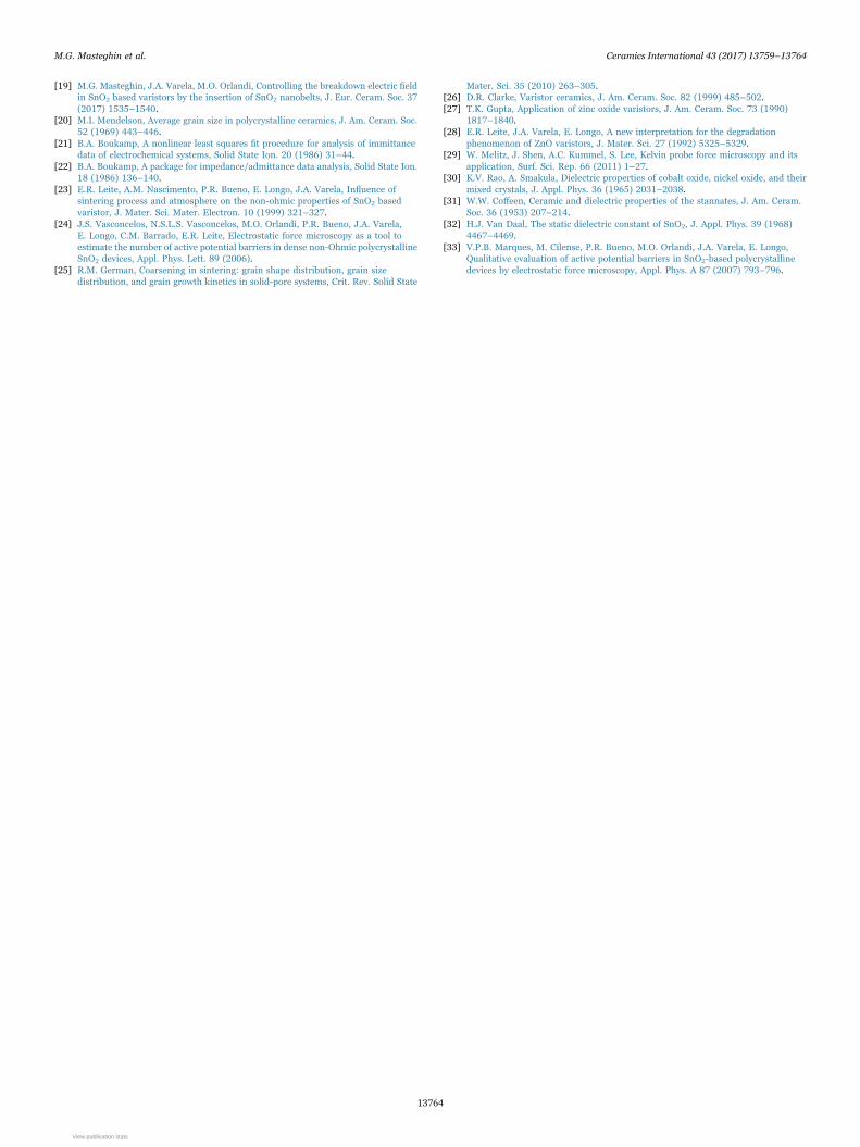
Impedance spectroscopy measurements were performed aiming ata further investigation of the varistor samples. The Nyquist plots of thestudied ceramics are presented in Fig. 5A, which also exhibits the datasimulation using the equivalent circuit shown in the inset. Theequivalent circuit consists of a resistor positioned in parallel to acapacitor (named Rgb and Cgb, respectively) representing the grainboundary where both of them are placed in parallel to a resistor inseries with a constant phase element (CPE) representing the internalelectron trap level.
Data simulation showed that the insertion of nanobelts wasresponsible for decreasing the grain boundary resistance in almostone order of magnitude, from 1.2 × 10⁶ Ω to 1.9 × 10⁵ Ω, by virtue ofthe percolation paths generated by the belts. Indeed, the reduction ingrain boundary resistance obtained in our investigation is quite close to
Table 2Nonlinear coefficient (α) and breakdown electric field (Eb) values obtained from dcmeasurements for the (98.90%)SnO2-(1.00%)CoO-(0.05%)Cr2O3-(0.05%)Nb2O5 system,without and with 1% wt. of nanobelts, sintered for 2 h at 1300 °C. Values from Pianarosystem [11] are included for comparison purposes.
Sample Nonlinear coefficient (α) Eb (V cm−1)
Without Nanobelts 18 1133Pianaro et al.’s system [11] 41 3990
With Nanobelts 26 270
Fig. 4. A1) Topography and B1) Capacitance gradient measurement (dC/dZ) of the sample without nanobelts. A2) Topography and B2) Capacitance gradient measurement (dC/dZ) ofthe sample with added belts (1 wt%).
M.G. Masteghin et al. Ceramics International 43 (2017) 13759–13764
13762
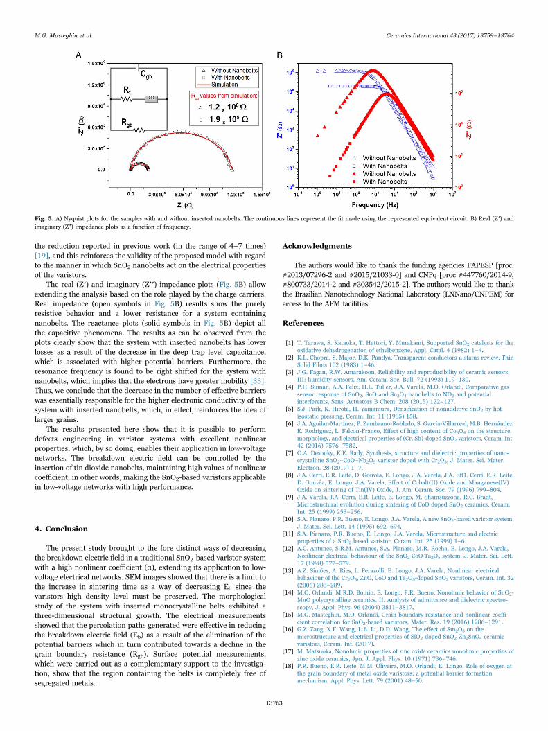
the reduction reported in previous work (in the range of 4–7 times)[19], and this reinforces the validity of the proposed model with regardto the manner in which SnO2 nanobelts act on the electrical propertiesof the varistors.
The real (Z′) and imaginary (Z′′) impedance plots (Fig. 5B) allowextending the analysis based on the role played by the charge carriers.Real impedance (open symbols in Fig. 5B) results show the purelyresistive behavior and a lower resistance for a system containingnanobelts. The reactance plots (solid symbols in Fig. 5B) depict allthe capacitive phenomena. The results as can be observed from theplots clearly show that the system with inserted nanobelts has lowerlosses as a result of the decrease in the deep trap level capacitance,which is associated with higher potential barriers. Furthermore, theresonance frequency is found to be right shifted for the system withnanobelts, which implies that the electrons have greater mobility [33].Thus, we conclude that the decrease in the number of effective barrierswas essentially responsible for the higher electronic conductivity of thesystem with inserted nanobelts, which, in effect, reinforces the idea oflarger grains.
The results presented here show that it is possible to performdefects engineering in varistor systems with excellent nonlinearproperties, which, by so doing, enables their application in low-voltagenetworks. The breakdown electric field can be controlled by theinsertion of tin dioxide nanobelts, maintaining high values of nonlinearcoefficient, in other words, making the SnO2-based varistors applicablein low-voltage networks with high performance.
4. Conclusion
The present study brought to the fore distinct ways of decreasingthe breakdown electric field in a traditional SnO2-based varistor systemwith a high nonlinear coefficient (α), extending its application to low-voltage electrical networks. SEM images showed that there is a limit tothe increase in sintering time as a way of decreasing Eb since thevaristors high density level must be preserved. The morphologicalstudy of the system with inserted monocrystalline belts exhibited athree-dimensional structural growth. The electrical measurementsshowed that the percolation paths generated were effective in reducingthe breakdown electric field (Eb) as a result of the elimination of thepotential barriers which in turn contributed towards a decline in thegrain boundary resistance (Rgb). Surface potential measurements,which were carried out as a complementary support to the investiga-tion, show that the region containing the belts is completely free ofsegregated metals.
Acknowledgments
The authors would like to thank the funding agencies FAPESP [proc.#2013/07296-2 and #2015/21033-0] and CNPq [proc #447760/2014-9,#800733/2014-2 and #303542/2015-2]. The authors would like to thankthe Brazilian Nanotechnology National Laboratory (LNNano/CNPEM) foraccess to the AFM facilities.
References
[1] T. Tarawa, S. Kataoka, T. Hattori, Y. Murakami, Supported SnO2 catalysts for theoxidative dehydrogenation of ethylbenzene, Appl. Catal. 4 (1982) 1–4.
[2] K.L. Chopra, S. Major, D.K. Pandya, Transparent conductors-a status review, ThinSolid Films 102 (1983) 1–46.
[3] J.G. Fagan, R.W. Amarakoon, Reliability and reproducibility of ceramic sensors.III: humidity sensors, Am. Ceram. Soc. Bull. 72 (1993) 119–130.
[4] P.H. Suman, A.A. Felix, H.L. Tuller, J.A. Varela, M.O. Orlandi, Comparative gassensor response of SnO2, SnO and Sn3O4 nanobelts to NO2 and potentialinterferents, Sens. Actuators B Chem. 208 (2015) 122–127.
[5] S.J. Park, K. Hirota, H. Yamamura, Densification of nonadditive SnO2 by hotisostatic pressing, Ceram. Int. 11 (1985) 158.
[6] J.A. Aguilar-Martínez, P. Zambrano-Robledo, S. García-Villarreal, M.B. Hernández,E. Rodríguez, L. Falcon-Franco, Effect of high content of Co3O4 on the structure,morphology, and electrical properties of (Cr, Sb)-doped SnO2 varistors, Ceram. Int.42 (2016) 7576–7582.
[7] O.A. Desouky, K.E. Rady, Synthesis, structure and dielectric properties of nano-crystalline SnO2–CoO–Nb2O5 varistor doped with Cr2O3, J. Mater. Sci. Mater.Electron. 28 (2017) 1–7.
[8] J.A. Cerri, E.R. Leite, D. Gouvêa, E. Longo, J.A. Varela, J.A. Eff1. Cerri, E.R. Leite,D. Gouvêa, E. Longo, J.A. Varela, Effect of Cobalt(II) Oxide and Manganese(IV)Oxide on sintering of Tin(IV) Oxide, J. Am. Ceram. Soc. 79 (1996) 799–804.
[9] J.A. Varela, J.A. Cerri, E.R. Leite, E. Longo, M. Shamsuzzoha, R.C. Bradt,Microstructural evolution during sintering of CoO doped SnO2 ceramics, Ceram.Int. 25 (1999) 253–256.
[10] S.A. Pianaro, P.R. Bueno, E. Longo, J.A. Varela, A new SnO2-based varistor system,J. Mater. Sci. Lett. 14 (1995) 692–694.
[11] S.A. Pianaro, P.R. Bueno, E. Longo, J.A. Varela, Microstructure and electricproperties of a SnO2 based varistor, Ceram. Int. 25 (1999) 1–6.
[12] A.C. Antunes, S.R.M. Antunes, S.A. Pianaro, M.R. Rocha, E. Longo, J.A. Varela,Nonlinear electrical behaviour of the SnO2·CoO·Ta2O5 system, J. Mater. Sci. Lett.17 (1998) 577–579.
[13] A.Z. Simões, A. Ries, L. Perazolli, E. Longo, J.A. Varela, Nonlinear electricalbehaviour of the Cr2O3, ZnO, CoO and Ta2O5-doped SnO2 varistors, Ceram. Int. 32(2006) 283–289.
[14] M.O. Orlandi, M.R.D. Bomio, E. Longo, P.R. Bueno, Nonohmic behavior of SnO2-MnO polycrystalline ceramics. II. Analysis of admittance and dielectric spectro-scopy, J. Appl. Phys. 96 (2004) 3811–3817.
[15] M.G. Masteghin, M.O. Orlandi, Grain-boundary resistance and nonlinear coeffi-cient correlation for SnO2-based varistors, Mater. Res. 19 (2016) 1286–1291.
[16] G.Z. Zang, X.F. Wang, L.B. Li, D.D. Wang, The effect of Sm2O3 on themicrostructure and electrical properties of SiO2-doped SnO2-Zn2SnO4 ceramicvaristors, Ceram. Int. (2017).
[17] M. Matsuoka, Nonohmic properties of zinc oxide ceramics nonohmic properties ofzinc oxide ceramics, Jpn. J. Appl. Phys. 10 (1971) 736–746.
[18] P.R. Bueno, E.R. Leite, M.M. Oliveira, M.O. Orlandi, E. Longo, Role of oxygen atthe grain boundary of metal oxide varistors: a potential barrier formationmechanism, Appl. Phys. Lett. 79 (2001) 48–50.
Fig. 5. A) Nyquist plots for the samples with and without inserted nanobelts. The continuous lines represent the fit made using the represented equivalent circuit. B) Real (Z′) andimaginary (Z") impedance plots as a function of frequency.
M.G. Masteghin et al. Ceramics International 43 (2017) 13759–13764
13763
[19] M.G. Masteghin, J.A. Varela, M.O. Orlandi, Controlling the breakdown electric fieldin SnO2 based varistors by the insertion of SnO2 nanobelts, J. Eur. Ceram. Soc. 37(2017) 1535–1540.
[20] M.I. Mendelson, Average grain size in polycrystalline ceramics, J. Am. Ceram. Soc.52 (1969) 443–446.
[21] B.A. Boukamp, A nonlinear least squares fit procedure for analysis of immittancedata of electrochemical systems, Solid State Ion. 20 (1986) 31–44.
[22] B.A. Boukamp, A package for impedance/admittance data analysis, Solid State Ion.18 (1986) 136–140.
[23] E.R. Leite, A.M. Nascimento, P.R. Bueno, E. Longo, J.A. Varela, Influence ofsintering process and atmosphere on the non-ohmic properties of SnO2 basedvaristor, J. Mater. Sci. Mater. Electron. 10 (1999) 321–327.
[24] J.S. Vasconcelos, N.S.L.S. Vasconcelos, M.O. Orlandi, P.R. Bueno, J.A. Varela,E. Longo, C.M. Barrado, E.R. Leite, Electrostatic force microscopy as a tool toestimate the number of active potential barriers in dense non-Ohmic polycrystallineSnO2 devices, Appl. Phys. Lett. 89 (2006).
[25] R.M. German, Coarsening in sintering: grain shape distribution, grain sizedistribution, and grain growth kinetics in solid-pore systems, Crit. Rev. Solid State
Mater. Sci. 35 (2010) 263–305.[26] D.R. Clarke, Varistor ceramics, J. Am. Ceram. Soc. 82 (1999) 485–502.[27] T.K. Gupta, Application of zinc oxide varistors, J. Am. Ceram. Soc. 73 (1990)
1817–1840.[28] E.R. Leite, J.A. Varela, E. Longo, A new interpretation for the degradation
phenomenon of ZnO varistors, J. Mater. Sci. 27 (1992) 5325–5329.[29] W. Melitz, J. Shen, A.C. Kummel, S. Lee, Kelvin probe force microscopy and its
application, Surf. Sci. Rep. 66 (2011) 1–27.[30] K.V. Rao, A. Smakula, Dielectric properties of cobalt oxide, nickel oxide, and their
mixed crystals, J. Appl. Phys. 36 (1965) 2031–2038.[31] W.W. Coffeen, Ceramic and dielectric properties of the stannates, J. Am. Ceram.
Soc. 36 (1953) 207–214.[32] H.J. Van Daal, The static dielectric constant of SnO2, J. Appl. Phys. 39 (1968)
4467–4469.[33] V.P.B. Marques, M. Cilense, P.R. Bueno, M.O. Orlandi, J.A. Varela, E. Longo,
Qualitative evaluation of active potential barriers in SnO2-based polycrystallinedevices by electrostatic force microscopy, Appl. Phys. A 87 (2007) 793–796.
M.G. Masteghin et al. Ceramics International 43 (2017) 13759–13764
13764
View publication statsView publication stats