high gain enhanced cmos charge pump with … · operation of charge pump circuit with ... cross...
TRANSCRIPT
International Research Journal of Engineering and Technology (IRJET) e-ISSN: 2395-0056
Volume: 02 Issue: 03 | June-2015 www.irjet.net p-ISSN: 2395-0072
© 2015, IRJET.NET- All Rights Reserved Page 2251
HIGH GAIN ENHANCED CMOS CHARGE PUMP WITH REDUCED LEAKAGE
AND THRESHOLD VOLTAGE
C.Arul murugan 1B.Banuselvasaraswathy 2 1Assistant professor, Department of Electronics and Telecommunication Engineering, Karpagam college of
Engineering, Coimbatore, 2Assistant professor, Department of Electronics and communication Engineering, Karpagam college of
Engineering,
Abstract—The charge pumps are based on the structure using MOS transistors as switches. However, the threshold voltage and body effect degrades the performance of the charge pump when the number of stages is raised. Hence, various charge pump topologies have been proposed to minimize the influence of body effect and threshold voltage. A CMOS charge pump of two phase non-overlapping clock signal generator was presented. Using these techniques, the proposed charge pump eliminates reversion loss and improves driving capability. It designed in 180-nm CMOS process in Cadence Virtuoso, whose evaluation results show that with no loading current, the proposed CMOS charge pump achieves an improvement of voltage conversion ratio and it also shows that the proposed charge pump has an improvement on current driving capability as compared with the conventional CMOS charge pumps.
Keywords—cross coupled charge pump, two phase
non-overlapping clock signal generator.
1. INTRODUCTION
Power consumption has been a major concern in
designing integrated circuits, due to the increased demand
for mobile devices, especially for driver circuits to drive
antenna switches, liquid crystal displays (LCDs), and
memories because all these components are integrated in
one mobile device to satisfy the customers’ demands. The
integration of various functional blocks led to the
shrinking feature size of a complementary metal oxide
semiconductor (CMOS) technology, and the scaling-down
resulted in a lower power supply voltage. Many driver
circuits require a higher voltage than a given power supply
voltage. To generate the high voltage in such circuits,
charge pumps are commonly used because they are small
in size and dissipate relatively small amount of power.
Charge pump circuits are widely applied in
Electrically Erasable Programmable Read-Only Memory
(EEPROM) and flash memories to provide voltages higher
than the supply voltage in order to program or erase
memory cells. CMOS charge pumps are used for generating
a high voltage from a low supply voltage. They are widely
used in ICs, such as flash memories, dynamic random
access memories (DRAMs), liquid crystal display panels,
and other mixed-mode systems. In DRAMs a group of
storage cell capacitors are connected to a bit-line through
nMOS switches, a charge pump can be used to generate a
word-line voltage higher than the supply voltage.
CMOS charge pumps consume a minimum current
in stand-by or power-down mode since they need to
maintain the output voltage. They are also required to
provide fast operation and large driving capability in
active mode where the charge pumps need to perform a
rapid voltage recovery and to supply sufficient amount of
charges to the load. CMOS charge pumps can be classified
as Dickson charge pumps and cross-coupled charge
pumps. Dickson charge pumps [2]–[5] are based on the
circuit proposed by Dickson, and adopt diode-connected
nMOS transistors as transfer switches. Although an nMOS
transfer switch provides higher carrier speed, the
threshold voltage drop through the switch severely limits
the output voltage level, resulting in pumping gain
degradation. Cross-coupled charge pumps [6]–[14]
normally adopt cross-coupled pMOS transistors as transfer
switches. A pMOS transfer switch has a benefit of
providing the output voltage without threshold voltage
drop. However, they have several issues related to
reversion loss and driving capability when the output
International Research Journal of Engineering and Technology (IRJET) e-ISSN: 2395-0056
Volume: 02 Issue: 03 | June-2015 www.irjet.net p-ISSN: 2395-0072
© 2015, IRJET.NET- All Rights Reserved Page 2252
voltage is low, which have become important issues in
mobile applications. For example, the reversion loss of
modern CMOS charge pumps should be minimized for
allowing less amount of current consumed in stand-by
mode. Charge driving capability of charge pumps should
also be enhanced as a large amount of charges need to be
consumed in active mode.
2. PROPOSED CP CIRCUIT
2.1. Operation of charge pump circuit with
simultaneous gate and substrate control
The simultaneous dynamic gate and substrate
control of the pMOS pass device NMn is realized by two
pairs of small auxiliary transistors (NMnn, NMpn) and
(NMsn1, NMsn2), respectively. The operation of the
proposed charge-transfer stage is synchronized with two-
phase complementary non overlapping clock signals qϕ1
and qϕ2. When qϕ2 = 0 and qϕ1 = VDD, capacitors CDn−1
and CDn are in the charging and charge-transfer phases,
respectively. As a result, voltage UVn−1 across capacitor
CDn−1 is charged to (n − 1)VDD and is the same as the
voltage Vn−2 across capacitor CDn−2 in the previous stage,
as CDn−2 is in the charge-transfer phase. On the other
hand, the voltage nVDD stored across capacitor CDn in the
previous half-clock period (charging phase) stacks on
voltage VDD of qϕ1 at the bottom plate of CDn such that
voltage UVn equals (n + 1)VDD. Noted that n is an integer
and is equal to 3 or above. In the dynamic gate control
block, since UVn is larger than UVn−1 by 2VDD, transistor
NMpn is on such that voltage VG = Vn = (n + 1)VDD.
Similarly, the source voltage of the nMOS transistor NMnn
is larger than its gate voltage Vn−1, so transistor NMnn is
off in this state. As the gate voltage VG of a pMOS pass
device NMn has the highest value, NMn is off. In the
dynamic substrate control block, pMOS transistor Msn1 is
off as its gate voltage VG is larger than its source voltage,
while NMsn2 is on as the magnitude of its gate-tosource
voltage is 2VDD. The body terminals of all pMOS
transistors NMpn, NMn, NMsn1, and NMsn2 are connected
to UVn via Msn2 and are thus biased at the highest voltage
potential of (n + 1)VDD in this state to eliminate the body
effect of transistor.
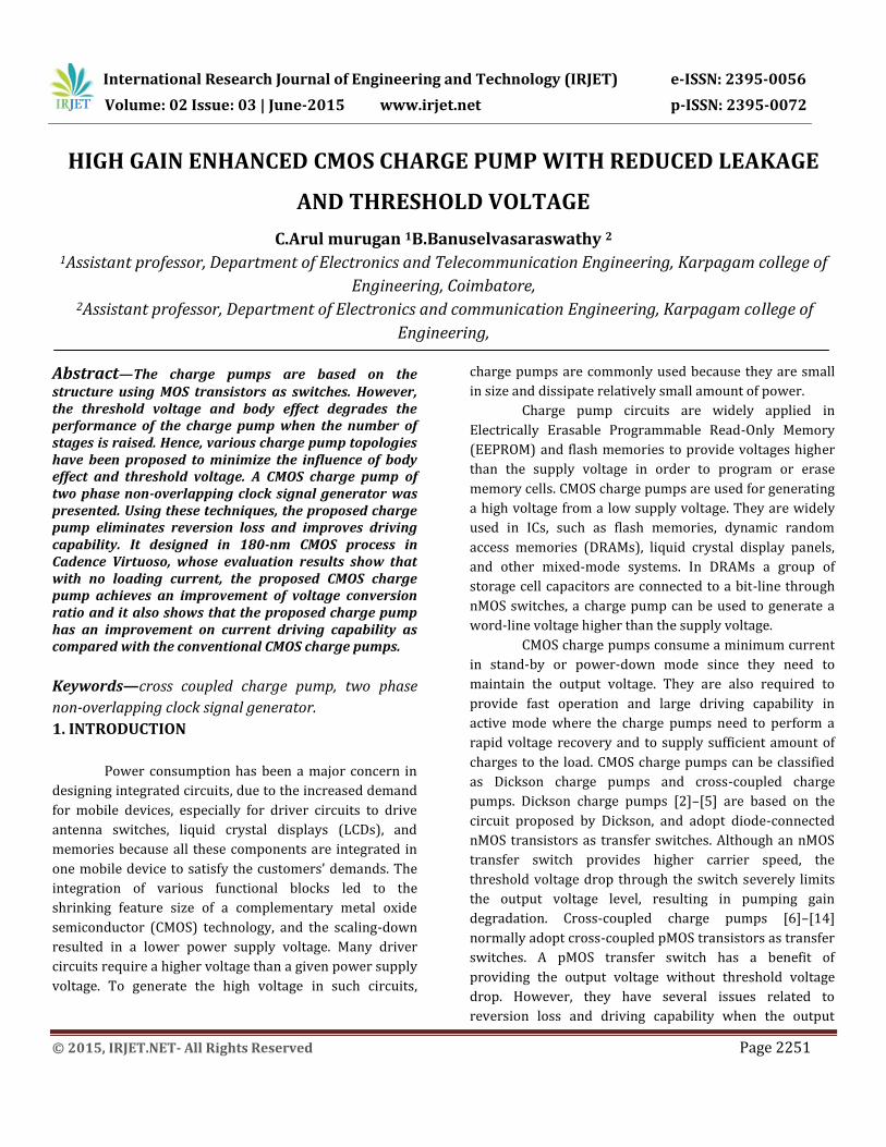
Fig.1. Charge pump cascade circuit
When qϕ2 = VDD and qϕ1 = 0, capacitors CDn−1
and CDn are in the charge-tansfer and charging phases,
respectively. Voltage UVn−1 is equal to nVDD, while
voltage UVn−2 across CDn−2 in the previous stage is (n −
2)VDD as CDn−2 is in the charging phase. Transistor NMnn
is thus turned on and causes VG = (n − 2)VDD. Since VG is
smaller than Vn−1 by 2VDD, transistor Mpn is off and pass
transistor NMn is on to enable the charge transfer from
Cn−1 to CDn such that UVn ≈ UVn−1 = nVDD.
In this phase, transistor Msn2 is off as its gate to-
source voltage is about zero, while Msn1 is on as the
magnitude of its gate-to-source voltage is 2VDD. Body
terminals of all pMOS transistors in this charge-transfer
stage are thus connected to the highest voltage potential of
Vn−1 = nVDD via Msn1. With the proposed simultaneous
dynamic gate and substrate control, Mn will be operated in
the deep triode region when it is on for the charge transfer.
The on-resistance Ron of Mn is given as
Ron =
where μp, Cox, W/L, and |Vthp| are the mobility, the
oxide capacitance, the device size, and the threshold
voltage of the pass transistor NMn, respectively. The
proposed dynamic substrate control always biases the
substrate voltage of NMn at the highest voltage potential
International Research Journal of Engineering and Technology (IRJET) e-ISSN: 2395-0056
Volume: 02 Issue: 03 | June-2015 www.irjet.net p-ISSN: 2395-0072
© 2015, IRJET.NET- All Rights Reserved Page 2253
under different clock phases to eliminate the body effect of
NMn under start-up and steady-state conditions. The value
of |Vthp| does not increase under changes of Vn−1 and Vn.
The dynamic substrate control is thus effective to lower
the value of Ron during charge transfer for improving the
voltage gain of the CP circuit. Note that the proper
substrate bias of all pMOS transistors provided by the
proposed dynamic substrate control can be achieved even
if NMn is in the deep triode region, while the previously
reported substrate control scheme properly works only if
NMn is a diode-connected device. The sizing of
NMsn1/NMsn2 is about 10 times smaller than that of NMn
in our design to reduce the input capacitance of
NMsn1/NMsn2. Hence, the switching loss due to
NMsn1and NMsn2 has negligible impact on the voltage
gain of the CP circuit
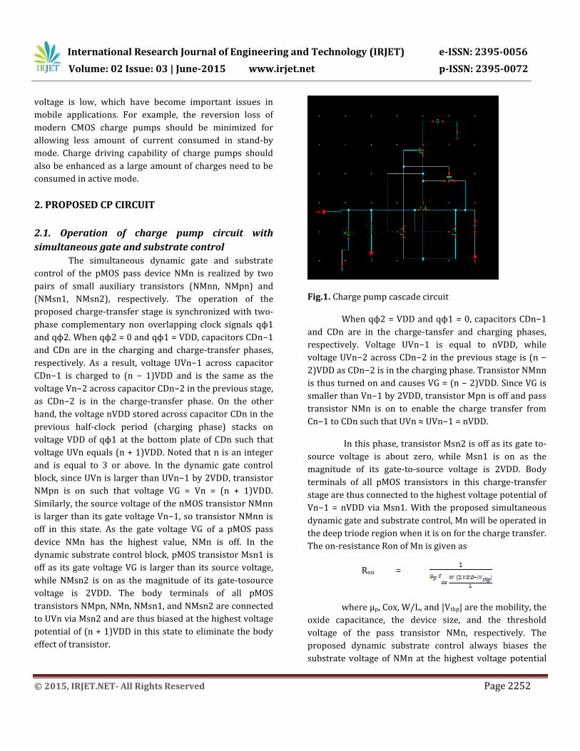
In addition, the proposed dynamic gate control
can further reduce the value of Ron during charge transfer
from CDn−1 to CDn by providing a large gate-to-source
voltage of 2VDD instead of VDD. The proposed scheme
with 2VDD driving is desirable for the CP circuit to achieve
a higher voltage gain due to lower Ron of pMOS pass
transistors under low input voltage condition compared to
the case of using VDD driving. It should be noted that, with
the use of the proposed charge-transfer stage in Fig. 2, the
largest gate-to-source voltage of the pMOS pass devices in
an N-stage CP circuit can still be kept at 2VDD. In this case,
as long as the input voltage VDD of the CP circuit is smaller
than half the gate-to-source breakdown voltage of the
pMOS pass transistor given in a technology node that
implements the CP circuit, the CP circuit satisfies the
requirement of gate-oxide reliability. For example, if a
standard pMOS transistor with its gate to- source
breakdown voltage of 5 V is used to implement the CP
circuit, the maximum input voltage of the CP circuit would
be 2.5 V by using the charge-transfer stage in Fig. 2 with
the proposed dynamic gate control scheme.
Fig.2. Cross coupled charge pump
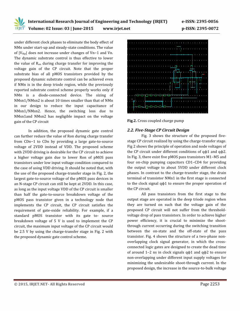
2.2. Five-Stage CP Circuit Design
Fig. 3 shows the structure of the proposed five-
stage CP circuit realized by using the charge-transfer stage.
Fig 2 shows the principle of operation and node voltages of
the CP circuit under different conditions of qϕ1 and qϕ2.
In Fig. 3, there exist five pMOS pass transistors M1–M5 and
four on-chip pumping capacitors CD1–CD4 for providing
the output voltage to about 5VDD under different clock
phases. In contrast to the charge-transfer stage, the drain
terminal of transistor NMn1 in the first stage is connected
to the clock signal qϕ1 to ensure the proper operation of
the CP circuit.
All pass transistors from the first stage to the
output stage are operated in the deep triode region when
they are turned on such that the voltage gain of the
proposed CP circuit will not suffer from the threshold-
voltage drop of pass transistors. In order to achieve higher
power efficiency, it is crucial to minimize the shoot-
through current occurring during the switching transition
between the on-state and the off-state of the pass
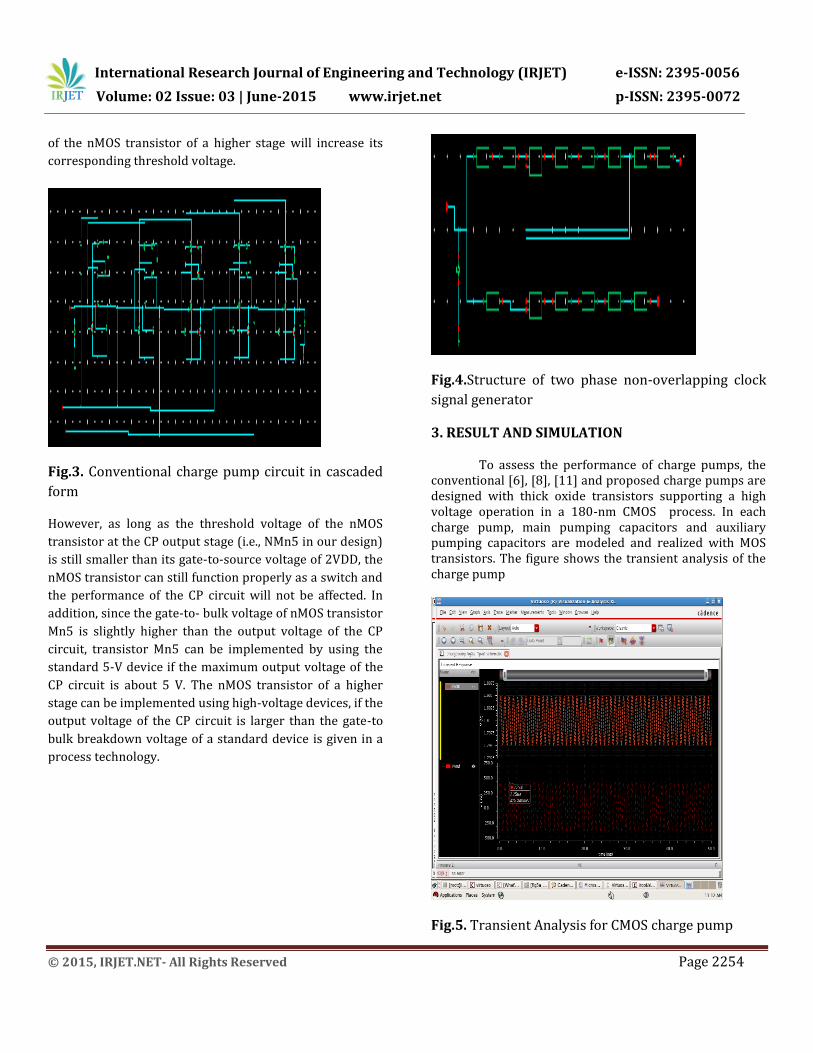
transistor. Fig. 4 shows the structure of a two-phase non-
overlapping clock signal generator, in which the cross-
connected logic gates are designed to create the dead time
of around 1–2 ns in clock signals qϕ1 and qϕ2 to ensure
non-overlapping under different input supply voltages for
minimizing the undesirable shoot-through current. In the
proposed design, the increase in the source-to-bulk voltage
International Research Journal of Engineering and Technology (IRJET) e-ISSN: 2395-0056
Volume: 02 Issue: 03 | June-2015 www.irjet.net p-ISSN: 2395-0072
© 2015, IRJET.NET- All Rights Reserved Page 2254
of the nMOS transistor of a higher stage will increase its
corresponding threshold voltage.
Fig.3. Conventional charge pump circuit in cascaded
form
However, as long as the threshold voltage of the nMOS
transistor at the CP output stage (i.e., NMn5 in our design)
is still smaller than its gate-to-source voltage of 2VDD, the
nMOS transistor can still function properly as a switch and
the performance of the CP circuit will not be affected. In
addition, since the gate-to- bulk voltage of nMOS transistor
Mn5 is slightly higher than the output voltage of the CP
circuit, transistor Mn5 can be implemented by using the
standard 5-V device if the maximum output voltage of the
CP circuit is about 5 V. The nMOS transistor of a higher
stage can be implemented using high-voltage devices, if the
output voltage of the CP circuit is larger than the gate-to
bulk breakdown voltage of a standard device is given in a
process technology.
Fig.4.Structure of two phase non-overlapping clock
signal generator
3. RESULT AND SIMULATION
To assess the performance of charge pumps, the conventional [6], [8], [11] and proposed charge pumps are designed with thick oxide transistors supporting a high voltage operation in a 180-nm CMOS process. In each charge pump, main pumping capacitors and auxiliary pumping capacitors are modeled and realized with MOS transistors. The figure shows the transient analysis of the charge pump
Fig.5. Transient Analysis for CMOS charge pump

International Research Journal of Engineering and Technology (IRJET) e-ISSN: 2395-0056
Volume: 02 Issue: 03 | June-2015 www.irjet.net p-ISSN: 2395-0072
© 2015, IRJET.NET- All Rights Reserved Page 2255
The performance comparison table is shown below
Table I- Performance comparisons
Proposed [2] [6] [8] [11]
Switch type
CMOS PMOs/ NMOS
PMOS PMOS PMOS
Voltage conversion
2 1.96 1.84 1.79 0.56
Iout ≤0.5
≤0.4 ≤0.36 ≤0.25 ≤0.18
Max Power Efficiency
0.4mA 0.3mA 0.26mA
0.21mA
0.15mA
Fig.6. Comparison Chart of voltage conversion
Here the voltage conversion of CMOS is 2 when using
PMOS / NMOS switch type the voltage conversion value is
1.96 and when using PMOS at different stages the value of
voltage conversion also varies according the stages
involved
Fig.6. Comparison Chart of Iout
The value of Iout in CMOS is less than 0.5, whereas either
using PMOS or NMOS at switching stages, its value is less
than or equal to 0.4 and when PMOS is used the value
decreases gradually from 0.36 to 0.25
Fig.6. Comparison Chart of Maximum Power
Efficiency
The efficiency of power obtained is 0.4mA
4. CONCLUSION
A high gain enhanced CMOS charge pump was
proposed to eliminate body effect and to minimize driving
capability for all the VLSI devices. For these features, a
CMOS charge pump of two phase non-overlapping clock
signal generator was designed using 180-nm CMOS
process in Cadence virtuoso tool. The results showed that

International Research Journal of Engineering and Technology (IRJET) e-ISSN: 2395-0056
Volume: 02 Issue: 03 | June-2015 www.irjet.net p-ISSN: 2395-0072
© 2015, IRJET.NET- All Rights Reserved Page 2256
the proposed charge pump provides improvements in
terms of voltage conversion ratio and current driving
capabilities.
REFERENCES
[1] Xiwen Zhang and Hoi Lee,” Gain-Enhanced Monolithic Charge Pump With Simultaneous Dynamic Gate and Substrate Control” IEEE Transactions On Very Large Scale Integration (Vlsi) Systems, Vol. 21, No. 3, March 2013 pp 593-596. [2] Joung-Yeal Kim, Su-Jin Park, Kee-Won Kwon, Bai-Sun Kong, Joo-Sun Choi, and Young-Hyun Jun,” CMOS Charge Pump With No Reversion Loss and Enhanced Drivability”, IEEE transactions on very large scale integration (vlsi) systems, pp 1-5. [3] G. D. Cataldo and G. Palumbo, “Double and triple charge pump for power IC: Dynamic models which take parasitic effects into account,” IEEE Trans. Circuits Syst. I, Fundam. Theory Appl., vol. 40, no. 2, pp. 92–101, Feb. 1993. [4] Y. Nakagome, H. Tanaka, K. Takeuchi, E. Kume, Y. Watanabe, T. Kaga, Y. Kawamoto, F. Murai, R. Izawa, D. Hisamoto, T. Kisu, T. Nishida, E. Takeda, and B. S. Kiyoo Itoh, “An experimental 1.5 V 64 Mb dram,” IEEE J. Solid-State Circuits, vol. 26, no. 4, pp. 465–472, Apr. 1991. [5] J.-T. Wu and K.-L. Chang, “MOS charge pumps for low-voltage operation,” IEEE J. Solid-State Circuits, vol. 33, no. 4, pp. 592–597, Apr. 1998. [6] P. Favrat, P. Deval, and M. J. Declercq, “A high-efficiency CMOS voltage doubler,” IEEE J. Solid-State Circuits, vol. 33, no. 3, pp. 410–416, Mar. 1998. [7] K.-S. Min, Y.-H. Kim, D. Kim, D. M. Kim, J.-H. Ahn, and J.-Y. Chung, “Efficient and large-current-output boosted voltage generators with non-overlapping-clock-driven auxiliary pumps for sub-1-V memory applications,” IEICE Trans. Electron., vol. E87-C, no. 7, pp. 1208–1213, Jul. 2004. [8] H. Lee and P. K. T. Mok, “Switching noise and shoot-through current reduction techniques for switched-capacitor voltage doubler,” IEEE J. Solid-State Circuits, vol. 40, no. 5, pp. 1136–1146, May 2005. [9] A. Fantini, A. Cabrini, and G. Torelli, “Impact of control signal nonidealties on two-phase charge pumps,” in Proc. IEEE Int. Symp. CircuitsSyst., May 2007, pp. 1549–15520. [10] F. Su, W.-H. Ki, and C.-Y. Tsui, “High efficiency cross-coupled doubler with no reversion loss,” in Proc. IEEE Int. Symp. Circuits Syst., May 2006, pp. 2761–2764.
[11] J.-Y. Kim, Y.-H. Jun, and B.-S. Kong, “CMOS charge pump with transfer blocking technique for no reversion loss and relaxed clock timing restriction,” IEEE Trans. Circuits Syst. II, Exp. Briefs, vol. 56, no. 1, pp. 11–15, Jan. 2009. [12] S.-I. Cho, J.-H. Lee, H.-J. Park, G.-H. Lim, and Y.-H. Kim, “Two-phase boosted voltage generator for low-voltage DRAMs,” IEEE J. Solid-State Circuits, vol. 38, no. 10, pp. 1726–1729, Oct. 2003. [13] K.-Y. Kim, Y. Kim, D.-C. Lee, Y.-R. Kang, H. Kim, S.-W. Kim and J. Park, “An energy efficient VPP generator with fast ramp-up time for mobile DRAM,” IEEE J. Solid-State Circuits, vol. 46, no. 6, pp. 1488–1494, Jun. 2011. [14] Y. C. Wong, N. H. Noordin, A. O. El-Rayis, N. Haridas, A. T. Erdogan,and T. Arslan, “An evaluation of 2-phase charge pump topologies with charge transfer switches for green mobile technology,” in Proc. IEEE Int. Symp. Ind. Electron., Jun. 2011, pp. 136–140. [15] J. Shin, I.-Y. Chung, Y. J. Park, and H. S. Min, “A new charge pump without degradation in threshold voltage due to body effect,” IEEE J. Solid-State Circuits, vol. 35, no. 8, pp. 1227–1230, Aug. 2000. [16] L. Mensi, L. Colalongo, A. Richelli, and Z. M. Kovács-Vajna, “Anew integrated charge pump architecture using dynamic biasing of pass transistors,” in Proc. Eur. Solid-State Circuits Conf., Sep. 2005, pp. 85–88. [17] J.-T. Wu and K.-L. Chang, “MOS charge pumps for low-voltage operation,” IEEE J. Solid-State Circuits, vol. 33, no. 4, pp. 592–597, Apr. 1998. [18] A. N. Richelli, L. Colalongo, L. Mensi, A. Cacciatori, and Z. M. Kovacs- Vajna, “Charge pump architectures based on dynamic gate control of the pass-transistors,” IEEE Trans. Very Large Scale Integr. (VLSI) Syst., vol. 17, no. 7, pp. 964–967, Jul. 2009. [19] G. Palumbo, D. Pappalardo, and M. Gaibotti, “Charge-pump circuits: Power-consumption optimization,” IEEE Trans. Circuits Syst.I, Fundam. Theory Appl., vol. 49, no. 11, pp. 1535–1542, Nov. 2002. [20] G. Palumbo and D. Pappalardo, “Charge pump circuits with onlycapacitive loads: Optimized design,” IEEE Trans. Circuits Syst. II, Exp. Briefs, vol. 53, no. 2, pp. 128–132, Feb. 2006.