high-frequency surface acoustic wave propagation …152818/datastream... · 1 high-frequency...
TRANSCRIPT
1
High-Frequency Surface Acoustic Wave Propagation in Nanostructures Characterized by Coherent Extreme Ultraviolet
Beams
Mark E. Siemens, Qing Li, Margaret. M. Murnane, and Henry C. Kapteyn
Department of Physics and JILA, University of Colorado, Boulder, CO 80309-0440
Ph. (303) 492-7764; FAX: (303) 492-5235; E-mail : [email protected]
Ronggui Yang
Department of Mechanical Engineering, University of Colorado, Boulder, CO 80309-0440
Erik H. Anderson
Center for X-Ray Optics, Lawrence Berkeley National Laboratory, Berkeley, CA 94720
Keith A. Nelson
Department of Chemistry, Massachusetts Institute of Technology, Cambridge, MA 02139
Abstract
We study ultrahigh frequency surface acoustic wave propagation in nickel-on-sapphire
nanostructures. The use of ultrafast, coherent, extreme ultraviolet beams allows us to extend
optical measurements of propagation dynamics of surface acoustic waves to frequencies of
nearly 50 GHz, corresponding to wavelengths as short as 125 nm. We repeat the measurement on
a sequence of nanostructured samples to observe surface acoustic wave dispersion in a
nanostructure series for the first time. These measurements are critical for accurate
characterization of thin films using this technique.

2
Monitoring surface acoustic wave (SAW) propagation is a powerful tool for studying the
properties of thin films, surfaces, and interfaces. SAW modes have a very shallow surface
penetration, and thus their propagation is sensitive to surface structure and composition. To study
films of sub-micron thickness, however, it is necessary to use SAWs with comparably short
wavelengths, since the penetration depth ζ of the SAW is proportional to the acoustic wavelength
Λ i.e. ζ = Λ/2π. This presents a challenge for conventional optical methods of creating and
detecting SAWs. Although it is quite straightforward to manufacture a sub-100nm thickness
film, thermally exciting the film using a visible light interference pattern in a transient grating
geometry is limited to SAW wavelengths in the range of optical wavelengths. As a result, the
shortest acoustic wavelength generated to-date using the transient grating method is
approximately 750nm [1, 2].
An alternative approach that overcomes this limitation is to lithographically pattern a
nanostructure on the surface. This pattern can then be optically excited, locally stressing a
surface and thus exciting a SAW with a wavelength limited only by the resolution of the
lithographic pattern [3, 4]. However, this approach raises the question of how much the presence
of the nanostructure will affect the propagation of the SAW. This question is critical for analysis
of the underlying sample characteristics. Past measurements employing thin Al patterned
absorbers suggested that these issues can be neglected [4-6]. However, these conclusions were
based on data taken at a single SAW wavelength. To date, no work has sampled the full
dispersion curve of a patterned thin film in order to come to a definitive conclusion on this issue.
Detection of very short-wavelength acoustic SAWs is also an issue. Visible light will not
diffract from a sub-wavelength structure, so current techniques measure very small (<1 part in
105 [7]) changes in surface reflectivity to observe SAW propagation [4-6]. However, these

3
reflectivity changes arise from a complex mix of thermal density changes and local and
interfacial stresses and strains. Direct transient grating diffraction from the surface would give
more reliable and easier-to-interpret data – however, such an experiment requires coherent light
with a wavelength shorter than the SAW wavelength. For high frequencies, this corresponds to
the extreme ultraviolet (EUV) region of the spectrum. In previous work, we demonstrated that
coherent EUV beams can very sensitively probe acoustic-induced surface displacements with
sub-picometer displacement resolution [8]. In that experiment, changes in the EUV diffraction
were due to thermal and acoustic surface displacement, while temperature and stress-induced
changes in reflectivity were negligible at the EUV wavelengths used (~29nm) [8].
In this work, we excite a series of nickel-on-sapphire nanostructures using a Ti:sapphire
laser, to generate high-frequency acoustic waves. We study the SAW propagation in the
nanostructures by observing the changing diffraction intensity of an EUV probe beam (see Fig.
1). We observe the highest-frequency SAW dynamics to-date and demonstrate a first
measurement of SAW dispersion in these nanostructure/bulk systems. We find that for long
acoustic wavelengths, the propagation of the SAW is dominated by propagation in the substrate,
with a SAW wavelength set by the nanostructure period. However, for shorter acoustic
wavelengths, the penetration depth decreases and the SAW is increasingly localized in the
nickel, slowing-down the SAW propagation. Our data are in excellent agreement with an
effective mass model for thin films, that have been modified to account for the presence of the
nanostructure.

4
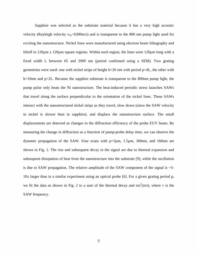
Figure 1: Setup for ultrafast SAW dispersion measurements. Nickel lines of thickness h = 10 or 20 nm, width L between 65 nm and 2 µm, and period p are patterned on a sapphire substrate. An 800 nm laser pulse (red) heats the Ni, creating a periodic stress that excites a SAW. This SAW is then probed by observing the dynamically changing diffraction of an ultrafast 29 nm EUV pulse (blue) from the surface.
The sample geometry is shown in Fig. 1. A laser heating beam and an EUV probe beam
both originate from an ultrafast Ti:Sapphire laser-amplifier system generating 2mJ, 25fs pulses at
a wavelength of 800nm and at a repetition rate of 2kHz. The output of this laser is split into
pump and probe beams. To generate the 29 nm probe beam, part of the 800 nm light is focused
into a gas-filled hollow waveguide to generate high-order harmonics, which are then refocused
onto the sample using a grazing-incidence toroidal mirror. The 800 nm pump beam is sent
through a computer-controlled time-delay stage before being loosely focused onto the sample. A
relatively large pump spot (~700µm) is used so that the area probed will see a uniform heating
fluence of 2mJ/cm.
5
Sapphire was selected as the substrate material because it has a very high acoustic
velocity (Rayleigh velocity vSa~6300m/s) and is transparent to the 800 nm pump light used for
exciting the nanostructure. Nickel lines were manufactured using electron beam lithography and
liftoff in 120µm x 120µm square regions. Within each region, the lines were 120µm long with a
fixed width L between 65 and 2000 nm (period confirmed using a SEM). Two grating
geometries were used: one with nickel strips of height h=20 nm with period p=4L, the other with
h=10nm and p=2L. Because the sapphire substrate is transparent to the 800nm pump light, the
pump pulse only heats the Ni nanostructure. The heat-induced periodic stress launches SAWs
that travel along the surface perpendicular to the orientation of the nickel lines. These SAWs
interact with the nanostructured nickel strips as they travel, slow down (since the SAW velocity
in nickel is slower than in sapphire), and displace the nanostructure surface. The small
displacements are detected as changes in the diffraction efficiency of the probe EUV beam. By
measuring the change in diffraction as a function of pump-probe delay time, we can observe the
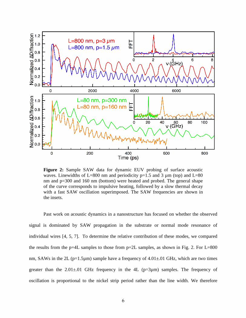
dynamic propagation of the SAW. Four scans with p=3µm, 1.5µm, 300nm, and 160nm are
shown in Fig. 2. The rise and subsequent decay in the signal are due to thermal expansion and
subsequent dissipation of heat from the nanostructure into the substrate [9], while the oscillation
is due to SAW propagation. The relative amplitude of the SAW component of the signal is ~5-
10x larger than in a similar experiment using an optical probe [6]. For a given grating period p,
we fit the data as shown in Fig. 2 to a sum of the thermal decay and sin2(πνt), where ν is the
SAW frequency.
6
Figure 2: Sample SAW data for dynamic EUV probing of surface acoustic waves. Linewidths of L=800 nm and periodicity p=1.5 and 3 µm (top) and L=80 nm and p=300 and 160 nm (bottom) were heated and probed. The general shape of the curve corresponds to impulsive heating, followed by a slow thermal decay with a fast SAW oscillation superimposed. The SAW frequencies are shown in the insets.
Past work on acoustic dynamics in a nanostructure has focused on whether the observed
signal is dominated by SAW propagation in the substrate or normal mode resonance of
individual wires [4, 5, 7]. To determine the relative contribution of these modes, we compared
the results from the p=4L samples to those from p=2L samples, as shown in Fig. 2. For L=800
nm, SAWs in the 2L (p=1.5µm) sample have a frequency of 4.01±.01 GHz, which are two times
greater than the 2.01±.01 GHz frequency in the 4L (p=3µm) samples. The frequency of
oscillation is proportional to the nickel strip period rather than the line width. We therefore
7
conclude that the oscillation is due to SAW propagation in the substrate, with a SAW wavelength
set by the strip period (Λ=p).
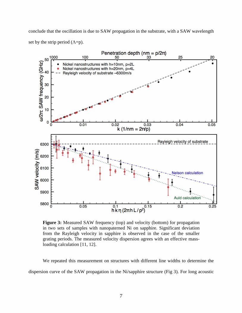
Figure 3: Measured SAW frequency (top) and velocity (bottom) for propagation in two sets of samples with nanopaterned Ni on sapphire. Significant deviation from the Rayleigh velocity in sapphire is observed in the case of the smaller grating periods. The measured velocity dispersion agrees with an effective mass-loading calculation [11, 12].
We repeated this measurement on structures with different line widths to determine the
dispersion curve of the SAW propagation in the Ni/sapphire structure (Fig 3). For long acoustic

8
wavelengths (large p, small k), the penetration depth is long, so the nanostructure can be ignored
and the SAW velocity is the Rayleigh velocity in the sapphire substrate i.e. frequency ν=vSa/p,
shown as a dashed line in Fig. 3. For shorter acoustic wavelengths, the penetration depth (see top
x-axis in Fig. 3) is decreased and the SAW is increasingly localized in the nickel, slowing-down
the SAW propagation. This velocity dispersion of SAWs with wavelengths as short as 125nm is
observed here for the first time in such nanostructures: previous studies of Al/quartz [5] and
Al/Si [6] structures at isolated acoustic wavelengths ~Λ>200nm suggested that the SAW
dispersion is minimal. The data show a small offset between the two different samples, which we
attribute to a small difference in the actual duty cycle. The ν=47 GHz frequency of the p=125nm
structure is the highest SAW frequency and shortest SAW wavelength measured optically.
A quantitative calculation of SAW propagation is complicated by the modified Brillouin
zone, stopbands, and multi-mode propagation introduced by the nanostructure [10]. To first
approximation, an effective mass model from thin film theory based on a perturbative expansion
of the stress at the surface can be used [11]. Datta and Hunsinger suggested an extension of this
thin film theory to nanostructures, introducing a duty cycle factor “η” (η=L/p) by which the
dispersion effect is multiplied [12]. Our data is in excellent agreement with this theory over the
entire range of wavelengths (Fig. 3, bottom). These results will be useful in eliminating
nanostructure-induced errors in similar measurements of thin film properties.
In conclusion, we used ultrafast, coherent, EUV beams to measure high frequency
surface acoustic wave propagation and dispersion in nanostructures at frequencies up to ~50
GHz for the first time. This technique of visible laser excitation and EUV probing can easily be
extended to even shorter wavelengths (higher frequencies), limited only by lithographic

9
capabilities. Thus, it holds promise for studying materials and interface properties of extremely
thin films and interfaces.
This work was supported by the Chemical Sciences, Geosciences, and Biosciences division of the Office of Basic
Energy Sciences, U.S. Department of Energy. This research made use of facilities supported by the NSF
Engineering Research Center in EUV Science and Technology. This work was supported by the Director,
Office of Science, Office of Basic Energy Sciences, of the U.S. Department of Energy under
Contract No. DE-AC02-05CH11231.

10
References
[1] J. A. Rogers, L. Dhar, and K. A. Nelson, “Noncontact determination of transverse isotropic
elastic moduli in polyimide thin films using a laser based ultrasonic method,” Applied Physics
Letters, 65(3):312, 1994.
[2] R. I. Tobey, M. E. Siemens, M. M. Murnane, H. C. Kapteyn, D. H. Torchinsky, and K. A.
Nelson, “Transient grating measurement of surface acoustic waves in thin metal films with
extreme ultraviolet radiation,” Applied Physics Letters, 89(9):091108, Aug 2006.
[3] R. I. Tobey, E. H. Gershgoren, M. E. Siemens, M. M. Murnane, H. C. Kapteyn, T. Feurer,
and K. A. Nelson. Nanoscale photothermal and photoacoustic transients probed with extreme
ultraviolet radiation. Applied Physics Letters, 85(4): 564–566, Jul 2004.
[4] G. A. Antonelli, P. Zannitto, and H. J. Maris, “New method for the generation of surface
acoustic waves of high frequency,” Physica B-Condensed Matter, 316:377, 2002.
[5] B. Bonello, A. Ajinou, V. Richard, P. Djemia, and S. M. Cherif, “Surface acoustic waves in
the ghz range generated by periodically patterned metallic stripes illuminated by an ultrashort
laser pulse,” JOSA, 110(4):1943, 2001.
[6] D. Hurley and K. Telschow, “Picosecond surface acoustic waves using a suboptical
wavelength absorption grating,” Physical Review B, 66:153301, 2002.
[7] H.-N. Lin, H. J. Maris, L. B. Freund, K. Y. Lee, H. Luhn, and D. P. Kern, “Study of
vibrational modes of gold nanostructures by picosecond ultrasonics,” J. of Applied Physics,
73:37, 1993.

11
[8] R. I. Tobey, M. E. Siemens, O. Cohen, M. M. Murnane, H. C. Kapteyn, and K. A. Nelson.
Ultrafast extreme ultraviolet holography: dynamic monitoring of surface deformation. Optics
Letters, 32(3):286–288, 2007.
[9] M. Siemens, Q. Li, M. Murnane, H. Kapteyn, R. Yang, E. Anderson, and K. Nelson, “Time-
resolved quasi-ballistic heat transport at nano-interfaces,” In preparation
[10] A. A. Maznev, “Band gaps and brekhovskikh attenuation of laser-generated surface
acoustic waves in a patterned thin film structure on silicon,” Physical Review B, 78:155323,
2008.
[11] B. A. Auld, Acoustic Fields and Waves in Solids, Wiley-Interscience, New York, 1973, Vol.
II, pages 275-283 and 302-309
[12] S. Datta and B. J. Hunsinger, “First-order reflection coefficient of surface acoustic waves
from thin-strip overlays,” Journal of Applied Physics, 50:5661, 1979.