high-brightness and low-voltage light-emitting devices
TRANSCRIPT
High-Brightness and Low-Voltage Light-EmittingDevices Based on Trischelated Ruthenium(II) and
Tris(2,2′-bipyridine)osmium(II) Emitter Layers and LowMelting Point Alloy Cathode Contacts
Frank G. Gao† and Allen J. Bard*,‡
Department of Chemistry & Biochemistry, The University of Texas at Austin,Austin, Texas 78712, and Wyle Laboratories, Mail Code BT-37, 1290 Hercules Drive,
Suite 120, Houston, Texas 77058
Received February 7, 2002. Revised Manuscript Received May 30, 2002
Solid-state light-emitting devices (LEDs) were fabricated based on an amorphous film ofRu(bpy)3(ClO4)2 (bpy ) 2,2′-bipyridine) about 100 nm thick on indium-tin oxide (ITO) withprinted low melting point alloys, such as Ga:In, Ga:Sn, and Bi:In:Pb:Sn, as cathodic contacts.A device with the structure of ITO (e10 Ω/square)/Ru(bpy)3(ClO4)2/Ga:Sn produces a brightred emission (3500 cd/m2 at 4.0 V) centered at 660 nm. This new method of making contactssignificantly simplifies the fabrication of an electroluminescence cell and has potentialapplication in the production of LEDs by inkjet or microcontact printing. LEDs based onC12-Ru(bpy)3(ClO4)2, Ru(phenanthroline)3(ClO4)2, and Os(bpy)3(PF6)2 were also studied. Lowmelting point alloy contacts were also used with cells based on tris(8-hydroxyquinoline)-aluminum.
Organic solid-state light-emitting devices (OLEDs)may eventually offer an alternative to inorganic semi-conductor (e.g., GaAs) light-emitting diodes and liquidcrystal displays, perhaps affording flatter, brighter, andmore flexible displays at lower cost.1-5 There has beena great deal of research aimed at the development ofnew light-emitting materials.6-19 Among the materialsthat have been studied, polymers based on trischelated
ruthenium(II) complexes have recently attracted con-siderable attention.20-26 Attempts have been made toincrease the duration of operation and to improve theperformance of light-emitting materials with dopant inthe emitters,27-30 dopant in the hole-transport mater-ials,31-34 electron-transport materials,35,36 transparent
* To whom correspondence should be addressed. Tel: (512) 471-3761. Fax: (512) 471-0088. E-mail: [email protected].
† Wyle Laboratories. Tel: (281) 483-5290 (office) and (281) 483-7299(lab). Fax: (281) 483-0402. E-mail: [email protected].
‡ The University of Texas at Austin.(1) Tang, C. W.; Vanslyke, S. A. Appl. Phys. Lett. 1987, 51, 913.(2) Burroughes, J. H.; Bradley, D. D. C.; Brown, A. R.; Marks, R.
N.; Mackay, K.; Friend, R. H.; Burns, P. L.; Holmes, A. B. Nature 1990,347, 539.
(3) Sheats, J. R.; Antoniadis, H.; Hueschen, M.; Leonard, W.; Miller,J.; Moon, R.; Roitman, D.; Stocking, A. Science 1996, 273, 884.
(4) Sheats, J. R.; Chang, Y.; Roitman, D. B.; Stocking, A. Acc. Chem.Res. 1999, 32, 193.
(5) Forrest, S. R. Chem. Rev. 1997, 97, 1793.(6) Yang, J. P.; Heremans, P. L.; Hoefnagels, R.; Tachelet, W.;
Dieltiens, P.; Blockhuys, F.; Geise, H. J.; Borghs, G. Synth. Met. 2000,108, 95.
(7) He, Y.; Kanick, J. Appl. Phys. Lett. 2000, 76, 661.(8) Baldo, M. A.; Lamansky, S.; Burrows, P. E.; Thompson, M. E.;
Forrest, S. R. Appl. Phys. Lett. 1999, 75, 4.(9) O’Brien, D. F.; Baldo, M. A.; Thompson, M. E.; Forrest, S. R.
Appl. Phys. Lett. 1999, 74, 442.(10) Tao, X. T.; Suzuki, H.; Wada, T.; Miyata, S.; Sasabe, H. J. Am.
Chem. Soc. 1999, 121, 9447.(11) Gigli, G.; Barbarella, G.; Favaretto, L.; Cacialli, F.; Cingolani,
R. Appl. Phys. Lett. 1999, 75, 439.(12) Berkovich, E.; Klein, J.; Sheradsky, T.; Silcoff, E. R.; Ranjit,
K. T.; Willner, I.; Nakhmanovich, G.; Gorelik, V.; Eichen, Y. Synth.Met. 1999, 107, 85.
(13) Curry, R. J.; Gillin, W. P. Appl. Phys. Lett. 1999, 75, 1380.(14) Xu, C.; Cui, Y.; Shen, Y.; Gu, H.; Pan, Y.; Li, Y. Appl. Phys.
Lett. 1999, 75, 1827.(15) Curry, R. J.; Gillin, W. P. Appl. Phys. Lett. 1999, 75, 1380.(16) Antoniadis, H.; Inbasekaran, M.; Woo, E. P. Appl. Phys. Lett.
1998, 73, 3055.
(17) Hamada, Y.; Kanno, H.; Sano, T.; Fujii, H.; Nishio, Y.;Takahashi, H.; Usuki, T.; Shibata, K. Appl. Phys. Lett. 1998, 72, 1939.
(18) Hamada, Y.; Sano, T.; Fujii, H.; Nishio, Y.; Takahashi, H.;Shibata, K. Appl. Phys. Lett. 1997, 71, 3338.
(19) Boyd, T. J.; Geerts, Y.; Lee, J.; Fogg, D. E.; Lavoie, G. G.;Schrock, R. R.; Rubner, M. F. Macromolecules 1997, 30, 3553.
(20) Maness, K. M.; Terrill, R. H.; Meyer, T. J.; Murray, R. W.;Wightman, R. M. J. Am. Chem. Soc. 1996, 118, 10609.
(21) Maness, K. M.; Masui, H.; Wightman, R. M.; Murray, R. W. J.Am. Chem. Soc. 1997, 119, 3987.
(22) Lyons, C. H.; Abbas, E. D.; Lee, J.-K.; Rubner, M. F. J. Am.Chem. Soc. 1998, 120, 12100.
(23) Handy, E. S.; Pal, A. J.; Rubner, M. F. J. Am. Chem. Soc. 1999,121, 3525.
(24) Wu, A.; Yoo, D.; Lee, J.-K.; Rubner, M. F. J. Am. Chem. Soc.1999, 121, 4883.
(25) Elliott, C. M.; Pichot, F.; Bloom, C. J.; Rider, L. S. J. Am. Chem.Soc. 1998, 120, 6781.
(26) Rubinstein, I.; Bard, A. J. J. Am. Chem. Soc. 1981, 103, 5007.(27) Hamada, Y.; Kanno, H.; Tsuyoshi, T.; Takahashi, H.; Usuki,
T. Appl. Phys. Lett. 1999, 75, 1682.(28) Sakamoto, G.; Adachi, C.; Koyama, T.; Taniguchi, Y.; Merritt,
C. D.; Murata, H.; Kafafi, Z. H. Appl. Phys. Lett. 1999, 75, 766.(29) Kido, J.; Hongawa, K.; Okuyama, K.; Nagai, K. Appl. Phys.
Lett. 1994, 64, 815.(30) Sato, Y.; Ogata, T.; Ichinosawa, S.; Murata, Y. Synth. Met.
1997, 91, 103.(31) Hu, N.; Xie, S.; Popovic, Z.; Ong, B.; Hor, A. J. Am. Chem. Soc.
1999, 121, 5097.(32) Chung, J.; Choi, B.; Lee, H. H. Appl. Phys. Lett. 1999, 74, 3645.(33) Blochwitz, J.; Pfeiffer, M.; Fritz, T.; Leo, K. Appl. Phys. Lett.
1998, 73, 729.(34) Yamamori, A.; Adachi, C.; Koyama, T.; Taniguchi, Y. Appl.
Phys. Chem. 1998, 72, 2147.(35) Donze, N.; Pechy, P.; Gratzel, M.; Schaer, M.; Zuppiroli, L.
Chem. Phys. Lett. 1999, 315, 405.(36) Jandke, M.; Strohriegl, P.; Berleb, S.; Werner, E.; Brutting,
W. Macromolecules 1998, 31, 6434.
3465Chem. Mater. 2002, 14, 3465-3470
10.1021/cm020117h CCC: $22.00 © 2002 American Chemical SocietyPublished on Web 07/13/2002
electrodes,37 and surface treatment of indium-tin oxide(ITO).38,39 Furthermore, with the realization that theoverall improvement of the performance and durabilityof LEDs is related to the improvement of the metalcontact, much research has been focused on understand-ing the nature of charge injection from contacts,4-42
metal diffusion and quenching of luminescence,43-45 andmodification of metal contacts.46-48 The method com-monly used to fabricate a cathodic metal contact relieson vacuum evaporation of low work function metals oralloys, such as Ca, Mg, Al, Ag, Mg:Ag, and Mg:In.
Like their polymer counterparts, LEDs employingsmall molecules as emitters have also been of com-mercial interest.1,6-10,13,15,17,18,27,49-52 In a recent paper,53
we reported on single-layer LEDs based on spin-coated
solid thin films of Ru(bpy)3(ClO4)2 (bpy ) 2,2′-bipyridine)with a cathodic contact achieved by printing of alow melting point alloy such as Ga:In, Ga:Sn, orBi:In:Pb:Sn. The current-voltage and luminance-volt-age plots show a diode-like behavior with a turn-onvoltage of 2.3 V. A brightness of up to 3500 cd/m2 at 4.0V bias and quantum and power efficiencies of 1.4% and0.8%, respectively, were realized. The emission spectrashowed a maximum at 640-660 nm, and the emissionwas clearly visible in a lighted room as a bright redemission. In this paper we describe the fabrication andtesting of such cells in further detail. Recent work onrelated cells has also appeared.54,55 LEDs based onC12-Ru(bpy)3(ClO4)2, Ru(phenanthroline)3(ClO4)2, andOs(bpy)3(PF6)2 are also discussed. We also show thatthis method of making cathodic contacts works withcells based on the more widely used tris(8-hydroxy-quinoline)aluminum (Alq3).
Experimental Section
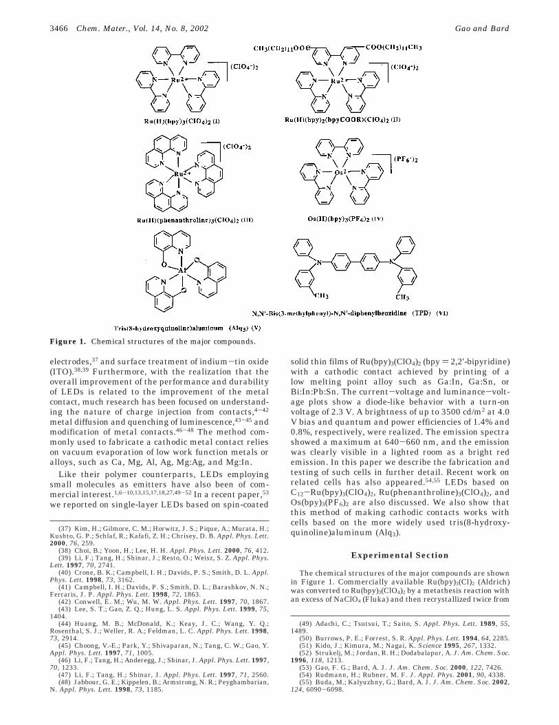
The chemical structures of the major compounds are shownin Figure 1. Commercially available Ru(bpy)3(Cl)2 (Aldrich)was converted to Ru(bpy)3(ClO4)2 by a metathesis reaction withan excess of NaClO4 (Fluka) and then recrystallized twice from
(37) Kim, H.; Gilmore, C. M.; Horwitz, J. S.; Pique, A.; Murata, H.;Kushto, G. P.; Schlaf, R.; Kafafi, Z. H.; Chrisey, D. B. Appl. Phys. Lett.2000, 76, 259.
(38) Choi, B.; Yoon, H.; Lee, H. H. Appl. Phys. Lett. 2000, 76, 412.(39) Li, F.; Tang, H.; Shinar, J.; Resto, O.; Weisz, S. Z. Appl. Phys.
Lett. 1997, 70, 2741.(40) Crone, B. K.; Campbell, I. H.; Davids, P. S.; Smith, D. L. Appl.
Phys. Lett. 1998, 73, 3162.(41) Campbell, I. H.; Davids, P. S.; Smith, D. L.; Barashkov, N. N.;
Ferraris, J. P. Appl. Phys. Lett. 1998, 72, 1863.(42) Conwell, E. M.; Wu, M. W. Appl. Phys. Lett. 1997, 70, 1867.(43) Lee, S. T.; Gao, Z. Q.; Hung, L. S. Appl. Phys. Lett. 1999, 75,
1404.(44) Huang, M. B.; McDonald, K.; Keay, J. C.; Wang, Y. Q.;
Rosenthal, S. J.; Weller, R. A.; Feldman, L. C. Appl. Phys. Lett. 1998,73, 2914.
(45) Choong, V.-E.; Park, Y.; Shivaparan, N.; Tang, C. W.; Gao, Y.Appl. Phys. Lett. 1997, 71, 1005.
(46) Li, F.; Tang, H.; Anderegg, J.; Shinar, J. Appl. Phys. Lett. 1997,70, 1233.
(47) Li, F.; Tang, H.; Shinar, J. Appl. Phys. Lett. 1997, 71, 2560.(48) Jabbour, G. E.; Kippelen, B.; Armstrong, N. R.; Peyghambarian,
N. Appl. Phys. Lett. 1998, 73, 1185.
(49) Adachi, C.; Tsutsui, T.; Saito, S. Appl. Phys. Lett. 1989, 55,1489.
(50) Burrows, P. E.; Forrest, S. R. Appl. Phys. Lett. 1994, 64, 2285.(51) Kido, J.; Kimura, M.; Nagai, K. Science 1995, 267, 1332.(52) Strukelj, M.; Jordan, R. H.; Dodabalapur, A. J. Am. Chem. Soc.
1996, 118, 1213.(53) Gao, F. G.; Bard, A. J. J. Am. Chem. Soc. 2000, 122, 7426.(54) Rudmann, H.; Rubner, M. F. J. Appl. Phys. 2001, 90, 4338.(55) Buda, M.; Kalyuzhny, G.; Bard, A. J. J. Am. Chem. Soc. 2002,
124, 6090-6098.
Figure 1. Chemical structures of the major compounds.
3466 Chem. Mater., Vol. 14, No. 8, 2002 Gao and Bard

an ethanol + acetone (5:1) solution.56 The perchlorate salt wasthen dried in a vacuum oven at 125 °C. The synthesis of thederivative C12-Ru(bpy)3(ClO4)2 followed the procedure re-ported previously.57 Ru(phenanthroline)3(ClO4)2 was preparedaccording to the same procedure,56 converted from com-mercially available Ru(phenanthroline)3(Cl)2 (Aldrich). Os-(bpy)3(PF6)2 was synthesized using a procedure describedelsewhere.58 N,N′-Bis(3-methylphenyl)-N,N′-diphenylbenzidine(TPD) and Alq3 were purchased from Aldrich. ITO substrates(1.6 × 2.2 cm2, Delta Technologies, Ltd., 100 Ω/square exceptwhere indicated) were cleaned by sonication in an 80 °Cethanolamine + H2O (20:80) bath for 20 min, then rinsed andsonicated several times in highly purified Millipore Milli-Qwater (18 MΩ cm), and dried in an oven at 95 °C. The structureof a single-layer LED cell is shown in Figure 2. Thin films(about 100 nm thick) of Ru(bpy)3(ClO4)2 were spin-coated ontoITO substrates from a 4% (w/v) acetonitrile (Burdick &Jackson, UV grade) solution at room temperature. The Ru-(bpy)3(ClO4)2 solution was first filtered through a 0.2 µm nylonsyringe to remove any large particles. Films were heated in avacuum oven at 125 °C for at least 8 h. Thin films (ca. 80 nmthick) of C12-Ru(bpy)3(ClO4)2 were spin-coated onto ITO sheetsfrom a 4% (w/v) pentanone solution. In some cells, TPD wasinserted between ITO and the emitter layer, where it func-tioned as a hole-transport layer. In these cells, a 0.7% TPD(w/v) xylene solution was used to form a 20 nm thin film byspin coating. Ga:In (75.5:24.5 wt %, mp 15.7 °C) and Ga:Sn(92:8 wt %, mp 20 °C) eutectic cathodes (ca. 3 mm diameter)were printed on the top of the films at room temperature usinga syringe and then connected via a thin copper wire insertedinto the Ga:In or Ga:Sn contact. Both were then sealed with 5min epoxy cement (Devcon, Danvers, MA). The light-emittingactive area (hereafter referred to as a contact) was about 7mm2. Usually four contacts were fabricated for each LED, i.e.,for each piece of ITO. In the preparation of the Bi:In:Pb:Sn(49:21:18:12 wt %, mp 58 °C) contact, the alloy was firstmelted, drawn into a syringe, kept in an oven at 80 °C, andthen printed on the top of the film. All eutectics werepurchased from Alfa Aesar. For comparison, vacuum-evapo-rated aluminum contacts were also fabricated. For single-layerLEDs based on Alq3, a thin film was spin-coated onto ITO froma saturated Alq3 pyridine solution. Then, the same procedureas that used in making a Ru(bpy)3(ClO4)2 device was followed.
Spin coating of the thin film was carried out by a Headwaymodel E101 spinner. All LEDs were fabricated in a laminar-flow hood under ambient conditions. Current-voltage, lumi-nance-voltage, current-time, and luminance-time charac-teristics were measured at room temperature with an AutolabGPES (General Purpose Electrochemical System, ECO ChemieBV, The Netherlands) and a Newport Optical Power Meter(model 1830-c) equipped with a 818-UV semiconductor detector(1 cm2) connected to the Autolab GPES via its auxiliary secondADC signal input ports. The reference and counter electrode
leads of the Autolab GPES potentiostat were connectedtogether to obtain the desired voltage at the LED electrodes.The emission spectra were measured with a model CH210CCD camera equipped with a monochromator and cooled to-125 °C. The optical absorption spectra were measured witha Milton Roy (San Leandro, CA) Spectronic 3000 diode arrayUV-vis spectrophotometer. Digital photographs and opticalmicroscopy were recorded with an Olympus BH-2 microscopeequipped with a Pixera digital visual system. Digital fluores-cence microscopy CCD pictures were taken with a confocaloptical microscope (Olympus SZX12) equipped with 470 nm(excitation) and 515 nm long-pass (emission) filters. Atomicforce microscopy (AFM) images were captured using a Nano-scope III with an AFM 619E-Z head (Digital Instruments,Santa Barbara, CA) using a SiN tip in the contact mode.Vacuum evaporation of Al contacts was carried out with anevaporator from Vacuum Engineering Co., Inc.
Results and Discussion
Ru(bpy)3(ClO4)2 Thin Film Characteristics. Fig-ure 3 is the optical absorption spectrum of a Ru(bpy)3-(ClO4)2 thin film on ITO, indicating a maximum ab-sorption at 455 nm. The optical microscope image of theRu(bpy)3(ClO4)2 thin film in Figure SI 1 shows arelatively smooth and uniform surface. The AFM imageof the film topography on ITO in Figure SI 2 (upper)shows a roughness of about 40 nm. A 100 nm thin filmthickness was determined by making a light scratch onthe surface and measuring the AFM line profile acrossit [Figure SI 2 (lower)].
A transmission electron microscope image of the Ru-(bpy)3(ClO4)2 films [Figure SI 3 (upper)] suggests thatthe films are amorphous [also confirmed by the X-raydiffraction pattern of the film, in Figure SI 2 (lower)].The Ru(bpy)3(ClO4)2 films are solid, i.e., contain no ortrace solvent, as can be seen from the differentialthermal analysis of the thin film in Figure SI 4.
Ru(bpy)3(ClO4)2-Based LEDs. Figure 4 (upper) isa photograph showing emission from two contacts of asingle-layer LED with the structure (+)ITO/Ru(bpy)3-(ClO4)2/Ga:In(-) at a voltage bias of 3.0 V. Unlessotherwise mentioned, the ITO contact in experimentswas positive, and this will be termed the forward biasdirection. The bright red emission was clearly visiblein a lighted room. A similar emission was obtained forthe LEDs using Ga:Sn, Bi:In:Pb:Sn, or Al as the contact.Figure 4 (lower) shows the emission spectrum of theLED using Ga:In as the cathodic contact, indicating amaximum emission at 660 nm, a half-maximum widthof 140 nm, and a relatively long tail toward the red.There was, at most, a very small (ca. 10 nm) blue shiftwhen the voltage bias increased from 3.1 to 9.4 V. Thisemission spectrum was essentially the same at thephotoluminescence spectrum of the thin film.
(56) McCord, P.; Bard, A. J. J. Electroanal. Chem. 1991, 318, 91.(57) Sprintschnik, G.; Sprintschnik, H. W.; Kirsch, P. P.; Whitten,
D. G. J. Am. Chem. Soc. 1977, 99, 4947.(58) Gaudiello, J. G.; Bradley, P. G.; Norton, K. A.; Woodruff, W.
H.; Bard, A. J. Inorg. Chem. 1984, 23, 3.
Figure 2. Structure of the single-layer LED cell.
Figure 3. Optical absorption spectrum of a Ru(bpy)3(ClO4)2
thin film on ITO.
Emitter Layers and Alloy Cathode Contacts Chem. Mater., Vol. 14, No. 8, 2002 3467

Figure 5 (upper) shows the current-voltage andluminance-voltage plots of a single-layer LED (+)ITO/Ru(bpy)3(ClO4)2/Ga:In(-) (forward bias). The LED showeda turn-on voltage of about 2.3 V for both current andemission. The device reached a luminance level of 500cd/m2 at 3 V and a maximum luminance of 2000 cd/m2
at about 4.5 V. Plots of external quantum efficiency andpower efficiency as a function of voltage bias in Figure5 (lower) show that with a voltage bias above 2.3 V thequantum efficiency and power efficiency rapidly increase
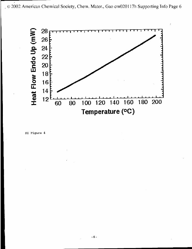
with voltage. At about 3.0 V, they reached maximumvalues of 1.4% and 0.8% (equivalent to about 1-2 lm/W), respectively, and then slowly decreased with afurther increase in voltage. Results from a group ofLEDs prepared by the same procedure showed consider-able variations in an external quantum efficiency rang-ing from 0.4% to 1.8% and power efficiencies from 0.2%to 1.2% [Figure SI 5 (upper and lower left)].
Figure 6 (upper) shows the current and luminancecurves vs time upon application of a 3.0 V voltage step.The time delay for the rise of the emission was onlyabout 0.02 s, with about 1-2 s needed to reach themaximum luminance output. Variations in delay timefor maximum emission were observed among the de-vices, ranging up to 1-5 s. The emission began todecrease soon after it reached the maximum, as shownby a time course of both the current and luminance[Figure 6 (lower)]. Typically, the luminance declined bymore than 50% in 1 h. The intensity of the emitted lightcontinued to decrease over several hours and thenmaintained a nearly steady level. After 5 h the emissionwas still visible with an intensity of about 20 cd/m2. Thehigher the applied voltage, the shorter the delay timefor the emission rise and the shorter the time foremission to decay to half its initial value. In contrast tothe rapid decrease of the luminance, the current fellslightly, if at all, during operation.
Influence of a TPD Hole-Transport Layer. Forcomparison, we also investigated LEDs with TPD as ahole transporter inserted between the ITO and theRu(bpy)3(ClO4)2 layer: (+)ITO/TPD/Ru(bpy)3(ClO4)2/Ga:In(-). Results of a group of 20 bilayer LEDs showedabout the same performance as that revealed in FigureSI 5 (right). Thus, a TPD layer did not significantlyimprove the performance of the LED cells in terms ofbrightness or lifetime. The performance appears to begoverned largely by the quality of the Ru(bpy)3(ClO4)2thin films formed on ITO substrates.
Influence of ITO Resistivity. We typically usedITO with a resistivity of 100 Ω/square. To understand
Figure 4. Photograph (upper) showing red emission from twocontacts of a single-layer LED ITO/Ru(bpy)3(ClO4)2/Ga:In.Emission spectrum of a single-layer LED ITO/Ru(bpy)3(ClO4)2/Ga:In (lower).
Figure 5. Current-voltage and luminance-voltage plots ofa single-layer LED (+)ITO/Ru(bpy)3(ClO4)2/Ga:In(-) (upper).The voltage scan rate was 0.05 V/s. External quantum ef-ficiency and power efficiency as a function of the voltage bias(lower).
Figure 6. Current and luminance transient curves uponapplication of a 3.0 V voltage bias for the LED ITO/Ru(bpy)3-(ClO4)2/Ga:In (upper). Same but over 2 h (lower).
3468 Chem. Mater., Vol. 14, No. 8, 2002 Gao and Bard

the influence of ITO resistivity on the performance ofLEDs, we tested similar LEDs fabricated by the sameprocess mentioned above but using 10 Ω/square ITOs.Figure 7 shows the current-voltage and luminance-voltage plots of a single-layer LED with the structureof (+)ITO (10 Ω/square)/Ru(bpy)3(ClO4)2/Ga:In(-). TheLED showed current-voltage and luminance-voltagebehavior very similar to those with 100 Ω/square ITO,though with a greater current density and hence emis-sion, at a relatively low field, reaching 3500 cd/m2 at4.0 V voltage bias. Quantum and power efficienciesshowed no improvement over those obtained using 100Ω/square ITO. For LEDs using more heavily In-doped10 Ω/square ITO, holes were injected more efficientlyfrom the ITO into the Ru(bpy)3(ClO4)2 layer, resultingin a significant increase of the intensities of current(injected holes from the anode and electrons from thecathode) and emission (by recombination of holes andelectrons).
Figure 8 indicates that a much higher current density(hence a greater emission intensity) was obtained withan LED (+)ITO/Au/Ru(bpy)3(ClO4)2/Ga:Sn(-), with abouta 10 nm semitransparent gold film inserted between theITO and the Ru(bpy)3(ClO4)2 film. For this device aluminance as high as 5000 cd/m2 at 3.5 V was realized.Gold, in all probability, is a better hole injectingmaterial than ITO. As a result, at the same field, moreholes were injected from the ITO/Au side into theRu(bpy)3(ClO4)2 film and, hence, more holes and elec-trons recombined, resulting in an enormous increase inboth current and emission. However, as with LEDsusing different ITOs, there was no significant differencein lifetime between the devices with an Au film insertedbetween the ITO and the Ru(bpy)3(ClO4)2 film and thosewithout one.
Different Cathodic Contacts. In addition to Ga:In, we used other low melting point alloys, Ga:Sn andBi:In:Pt:Sn, as cathodic contacts. Figure SI 6 is aphotograph showing emission from two contacts of asingle-layer LED with the structure ITO/Ru(bpy)3-(ClO4)2/Ga:Sn(-) at 3.0 V. The bright red emission wasclearly visible in a lighted room. Figure SI 6 (lower) isa photograph showing emission from two contacts of asingle-layer LED ITO/Ru(bpy)3(ClO4)2/Bi:In:Pt:Sn at 3.0V. Ru(bpy)3(ClO4)2-based LEDs using Ga:In, Ga:Sn, andBi:In:Pt:Sn as cathodic contacts show very similarperformances in current-voltage and luminance-volt-age behavior, turn-on voltage, and emission spectra.Evaporated Al and printed Hg were also used ascathodic contacts, and visible red emissions were ob-tained for those LEDs using Al and Hg contacts.
Mechanism of Electroluminescence (EL). Wepresent a detailed model of the EL process in these filmselsewhere.55 In brief, the EL mechanism in the solidstate is proposed to occur by an electrochemical process,similar to the electrogenerated chemiluminescence (ECL)mechanism in solution arising from the annihilation ofRu(bpy)3
3+ (holes in the solid state residing mainly onthe Ru) and Ru(bpy)3
+ (electrons in the solid stateresiding mainly on the bipyridines). As described else-where,55 establishment of the needed fields at bothcontacts requires some mobility of the ClO4
- withelectrons injected from the cathode and holes from theanode. Hopping of holes and electrons, betweenRu(bpy)32+ sites, forms RuIII(bpy)33+ and RuII(bpy)2(bpy-)+
sites, and where these meet in the film, the annihilationreaction produces RuII(bpy)3
2+*. The balance betweenelectron injection and hole injection governs the quan-tum efficiency; excess electrons or holes migrate to theopposite electrode without undergoing the annihilationreaction.
Mechanism of Emission Decay. An importantproblem with the possible application of Ru(bpy)3-(ClO4)2-based LEDs is their relatively short lifetime (onthe order of a few hours), and experiments wereundertaken to understand the emission decay mecha-nism. Because the results discussed above were ob-tained with LEDs fabricated and tested under ambientconditions, we tested LEDs, formed by spin coating inthe ambient, in a dry Ar atmosphere but found nosignificant improvement in lifetime. We also changedanode materials from ITO to ATO (antimony-dopedtin oxide) and Au, again noting no improvement inemission lifetime. Furthermore, we found that LEDsusing various cathodic contacts, such as Ga:In, Ga:Sn,Bi:In:Pt:Sn, Al, and Hg cathode contacts, showed similaremission decays.
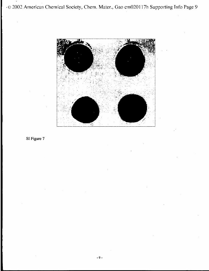
We also studied the effect of cell operation lifetimeon the photoluminescence of the film. Figure SI 7 is aphotoluminescence confocal microscope CCD picture ofa four-contact LED (+)ITO/Ru(bpy)3(ClO4)2/Ga:Sn(-).The contact at the upper right corner, operated for 100h at 4.5 V bias, showed no or very weak fluorescence,while the other contacts that remained at open circuitshowed intense red-orange emission. The emissionintensity decreased with operation time and was notice-ably decreased after 1 h of operation and almostcompletely quenched after 72 h (Figure SI 8).
Figure 7. Current-voltage and luminance-voltage plots ofa single-layer LED using 10 Ω/square ITO as the substrate,i.e., ITO (10 Ω/square)/Ru(bpy)3(ClO4)2/Ga:In. The voltage scanrate was 0.05 V/s.
Figure 8. Current-voltage and luminance-voltage plots ofa single-layer LED with a semitransparent gold layer insertedbetween ITO and the emitter layer, i.e., ITO/Au/Ru(bpy)3-(ClO4)2/Ga:In. The voltage scan rate was 0.05 V/s.
Emitter Layers and Alloy Cathode Contacts Chem. Mater., Vol. 14, No. 8, 2002 3469

The Ru(bpy)3(ClO4)2 compound itself is thermallystable and does not appear to decompose after 100 h ofoperation. Figure 9 (dotted line) shows the opticalabsorption spectrum of a fresh ITO/Ru(bpy)3(ClO4)2 filmbefore operation. A Hg contact was made to the sameITO/Ru(bpy)3(ClO4)2 film and an 8.0 V voltage bias wasapplied, resulting in a bright red emission whichdecayed with time. After 5 h of operation, the Hg contactwas removed and the optical absorption spectrum of theITO/Ru(bpy)3(ClO4)2 film in the same region was mea-sured again. This is shown in Figure 9 (solid line). Nosignificant decrease in the absorbance of Ru(bpy)3(ClO4)2was observed. However, the optical absorption spectrumof the film after operation showed two peaks.
The results suggest the buildup of a quencher duringoperation. It is also possible that migration of metal ionsfrom the contacts into the film and impurities in thefilm play a role in the process. Further experimentsalong these lines are currently underway.
C12-Ru(bpy)3(ClO4)2 and Ru(phenanthroline)3-(ClO4)2. We also fabricated LEDs with a spin-coatedsingle layer of C12-Ru(bpy)3(ClO4)2 or Ru(phenanthro-line)3(ClO4)2 as the emitter and printed Ga:Sn as thecathodic contact. Although a clearly visible red emissionwas generated for both LEDs, their luminance andefficiencies are much less than those using Ru(bpy)3-(ClO4)2 as the emitter. The emission spectra of two LEDsusing C12-Ru(bpy)3(ClO4)2 and Ru(phenanthroline)3-(ClO4)2, respectively, are given in Figures SI 9 and SI10.
Os(bpy)3(PF6)2. Red emission is seen from the single-layer LED (+)ITO/Os(bpy)3(PF6)2/Ga:Sn(-) (see FigureSI 11). The lower part of Figure SI 11 shows theemission spectrum of this LED, with a maximum atabout 700 nm. Although the intensity and efficiency ofthese cells was also much smaller than those obtainedusing Ru(bpy)3(ClO4)2 as the emitter, the emissionlifetime was much longer. Figure 10 shows the timecourse of the current and luminescence.
Alq3. Alq3 has been extensively studied as a compo-nent of LEDs. These cells behave as typical semiconduc-tor LEDs and utilize low work function cathodes, likeCa. Low melting point alloys as cathodic contacts havenot been investigated. To see if such a cathode would
work, a single-layer LED, (+)ITO/Alq3/Ga:Sn(-), wasconstructed. This emitted visible green-yellow light uponthe application of a forward voltage bias. Its emissionspectrum, with a maximum at 550 nm, is shown inFigure 11. Printed low melting point alloys may, there-fore, prove useful in LEDs employing small molecules,or perhaps polymers, as light emitters.
Conclusions
We have demonstrated high brightness (3500 cd/m2
at 4.0 V) and low voltage driven LEDs (turn-on voltageof 2.3 V) based on an amorphous film of Ru(bpy)3(ClO4)2as the emitter and using printed low melting pointalloys such as Ga:In, Ga:Sn, and Bi:In:Pb:Sn as cathodiccontacts. The relatively short emission lifetime (hours)is probably due to quenching of the Ru(bpy)3(ClO4)2excited state by species formed in the film duringoperation.
Acknowledgment. We are grateful to Dr. John T.McDevitt and Dr. Yi Deng for the use of their confocalmicroscope and their help with the microscope pictures;to Dr. Michael Brown and Dr. Dwight Romanovicz fortheir help in measuring the TEM images; and to Dr.Hyacinth Cabibil for help in measuring the thin filmthickness with AFM. The support of this research bythe Department of Defense MURI and the TexasAdvanced Research Program is gratefully acknowl-edged.
Supporting Information Available: This material isavailable free of charge via the Internet at http://pubs.acs.org.
CM020117H
Figure 9. Optical absorption spectrum of an ITO/Ru(bpy)3-(ClO4)2 film before operation (dotted line). In the same area, aHg contact was made, and a 8.0 V voltage bias was added for5 h, then the Hg contact was removed, and an opticalabsorption spectrum of the ITO/Ru(bpy)3(ClO4)2 film in thesame area was measured (solid line).
Figure 10. Current and luminance curves against time uponapplication of 5.0 V voltage bias for the LED ITO/Os(bpy)3-(PF6)2/Ga:Sn.
Figure 11. Emission spectrum of a single-layer LED ITO/Alq3/Ga:Sn.
3470 Chem. Mater., Vol. 14, No. 8, 2002 Gao and Bard