hf receiver platform
TRANSCRIPT

HF Receiver Experimenter Platform – O16
HF Receiver Platform
A little background information
Many thanks for purchasing this HF Receiver Platform PCB.
This experimenters PCB is available in three forms, 1) bare PCB 2) bare PCB and component set & 3) built & tested unit. These instructions and guide to use, provide all the information required, whatever version has been purchased.
The design provides a fully functional receiver that can be used (as supplied) to receive WWV time signals on 10.0000 MHz, or by addition of a local oscillator a receiver that can be used to monitor the HF bands from approx. 2 MHz – 18 MHz
The receivers open architecture allows experimentation with front end RF amplifiers/pre-selectors, audio processors at the amplifier stage and of course variable oscillator (VFO) experiments. See the ‘Experimenter Section’ for more on this and other ideas.
Direct Conversion Receiver notes Direct conversion (DC) receivers take the incoming signal at its signal frequency and process it to the
audio amplifier without the need for separate intermediate frequency (IF) oscillators. This has the
advantage of being able to resolve AM, CW and SSB signals without the use of a separate BFO, or
other oscillators.
DC receivers are also generally simpler to build and get operational, demonstrate good sensitivity, and
are easy to operate. Disadvantages are that DC receivers can be overwhelmed by strong AM signals,
and can be prone to AC Hum pickup and microphonics (microphonics is where components on the
board act as audio pickups and tapping them can lead to an annoying thump being heard in the
speaker).
Our design is very immune to microphonics and AC Hum pickup, it can still pickup strong AM
broadcasts especially after dark, however, this can be reduced by installing the PCB in a metal
enclosure.
Circuit operation This design is a Direct Conversion style radio using the common SA602N & LM386 combination.
The receiver is powered by 9-12 volts dc applied to the center positive 5.1mm barrel jack, this voltage
is fed via a 1N4001 reverse polarity protection diode to Pin 6 of the LM386 amplifier, then via R2 (270

HF Receiver Experimenter Platform – O16
Ohms) to a 6.2 volt Zener diode that feeds pin 8 of the SA602N, and also a LM78L05 5 volt regulator
that provides 5 volts to the on board block oscillator if used.
The BNC antenna jack connects to the antenna, and feeds the RF gain potentiometer via a 0.1uF
capacitor, the RF gain potentiometer acts as a simple signal attenuator. This signal then passes to L3 a
10MHz IF transformer whose secondary connects to pins 1 &2 of the SA602N, this transformer peaks
the incoming RF.
If the on-board 10 MHz block oscillator is being used, the oscillator output, after signal conditioning
via L1, L2 and C12, C13, C14 is applied to pins 6 & 7 of the SA602N. A 50 Ohm terminating resistor is
included in kits and installed on finished boards to prevent issues created by an the LO port being left
unterminated. Received audio then appears at pins 4 & 5 of the SA602N and is fed to the LM386
amplifier via the AF gain potentiometer, which acts as a volume control.
The LM386 is configured in its basic gain form; an extra 10uF electrolytic capacitor can be installed at
the C10 position if increased gain is required. Amplified audio appears at the 3.5mm jack socket. This
can drive a small 8 Ohm speaker, or smartphone ear buds very satisfactorily. The use of powered
computer speakers provides a good solution also.
A Local Oscillator inject SMA socket is also available to allow an external VFO, DDS VFO, or other
signal generator to be applied to the receiver.
Please Note:
If an external VFO/DDS is used, the on board block oscillator needs to be removed first.
First time use/set-up As supplied (or if built from the kit components), the receiver is ready to be used. External
connections required will be a 12 Volts DC power supply, speaker or headset, antenna, outdoor is
preferred, and if possible a ground connection.
Ensure the 10MHz block oscillator is properly seated in its socket, double check the orientation and
that oscillator pins are seated in their respective socket pinholes and not bent under.
The antenna is connected to the BNC jack, power is applied to the 5.1mm barrel jack (center positive)
and speakers or headset to the 3.5mm jack.
Before actually applying power, set each potentiometer to its mid-point setting, a positive feel detent
at the mid-point will help in setting this point.

HF Receiver Experimenter Platform – O16
Apply power and advance the AF gain potentiometer to a comfortable listening level, the distinctive
signal from WWV (or WWVH) should be heard which comprises a regular ‘tick’ and voice
announcements. If no signal is heard, advance the RF gain control towards its maximum position. As
the RF gain control is a simple attenuator always set it to the position that allows the best reception
of the desired signal and attenuation of any interfering stations.
Remember that WWV transmits on the HF bands; as such it is affected by the same propagation issues
that can affect all HF transmissions. On some occasions the signal will be strong and the received
signal will be loud and clear – on other occasions it will be weaker and strong hiss or other QRM may
be experienced. Reception conditions aside, the time of day can also have a bearing on the quality of
the received signal as well as the season. In general, daytime will give best results and Spring/Summer
the best days.
Antenna Selection For best results an outdoor antenna should be used – a dipole strung as high as possible or end fed
long wire will give best results. Location in regards to the transmitter location (Fort Collins Colorado
for WWV & Hawaii for WWVH) will also have an effect and also orientation of the antenna to the
signal transmitter can be worth experimenting with.
An indoor antenna can work as well, locating the antenna in an attic or loft space can improve
reception, however, it may also introduce local electrical noise if near household wiring.
Kit Builders Instructions If you have purchased just the bare PCB or a PCB with the components and intend to assemble the
receiver yourself start here.
This section will outline the components used and where to purchase the components.
Experienced constructors may want to check out the ‘Experimenter Section’ before starting so they
can consider including some of the suggested modifications.
While the PCB is a relatively simple layout and quite easy to assemble in a few hours of work, it is not
a beginners project and some experience with assembling and soldering electronics is recommended.
The chart on the next page details all the components, their PCB location and suggested supplier with
order code.
Start by opening the bags of supplied components and checking the items received against the chart.
Please contact us immediately if any parts are missing: [email protected]

HF Receiver Experimenter Platform – O16
Component Parts List
Part No Part Location
Part Value Supplier
Name Supplier Order code Notes
1 R1 270 Ohm Mouser 603-MFR505FTE52-270R
2 R2 10K Ohm Mouser Not supplied/installed Replace with wire link
3 C1 0.1uF Mouser 581-SR215C104KAATRI
4 C2 0.01uF Jameco 15231
5 C3 75pF Mouser 80-C322C750JCG
6 C4 75pF Mouser 80-C322C750JCG
7 C5 0.01uF Jameco 15231
8 C6 10uF Jameco 94212 Install to increase AF Gain
9 C7 100uF Mouser 667-ECA-1VM101
10 C8 100uF Mouser 667-ECA-1VM101
11 C9 10uF Jameco 94212
12 C10 10uF Jameco 94212
13 C11 10uF Jameco 94212
14 C12 270pF Mouser 810-FK28COG1H271J
15 C13 470pF Mouser 810-FK28COG1H471J
16 C14 270pF Mouser 810-FK28COG1H271J
17 C15 0.001uF Jameco 1947343
18 L1 1uH Mouser 70-IM02EB1R0K
19 L2 1uH Mouser 70-IM02EB1R0K
20 L3 421-123 IF ER - Supplied with bare PCB
21 ICI SA602N Jameco 1367795
22 U1 LM386-3 Jameco 24133
23 QG1 10MHz Xtal Digikey CTX772-ND
24 J1 5.1mm Jameco 101178
25 JP1 3.5mm Mouser 502-35RAPC4BHN2
26 X1 SMA Mouser 530-142-0701-201
27 X2 SMA Mouser - Not supplied/installed
28 Antenna BNC Mouser 523-31-5431-10RFX
29 Socket Xtal SKT. Jameco 133006
30 D1 6.2V Zener Mouser 512-1N5234BTR
31 D2 1N4001 Mouser 512-1N4001
32 - PCB ER ER-WWV-PCB Supplied with Kits
33 RV1 10K Pot. Mouser 667-EVU-F3MFL3B14
34 RV2 10k Pot Mouser 667-EVU-F3MFL3B14
35 IC3 78L05 Mouser 511-L78L05ACZ-AP

HF Receiver Experimenter Platform – O16
Stage 1 – Build the Power Supply
Start construction by soldering the diodes D1 & D2 (note orientation) then capacitors C9 &C11, these
are also polarized so note orientation as marked on the board. Insert IC3, ensuring the orientation flat
on the IC matches the print on the PCB. Now add the resistor R2 and the barrel jack. This completes
the power supply section, by applying 12 volts to the barrel jack (center positive) and referring to the
Stage 2 photo check the correct voltages are at the test points shown.

HF Receiver Experimenter Platform – O16
Stage 2 – Voltage checks With power applied to the barrel jack, probe the board as indicated with your meter set to 20 volts DC
range. Apply the black probe to the ground plane and the positive or Red probe to measure voltages:
5 Volts DC at the oscillator
Input voltage at Pin 6 of the LM386
6-6.2 Volts at Pin 8 of theSA602N
If all voltages check out correctly, you are ready to move to the next stage, if not recheck your work.

HF Receiver Experimenter Platform – O16
Stage 3 – Add capacitors For this stage we are adding C1, C2, C3, C4, C5, C6, C7, C8, C12, C13, C14, and C15. Note C10 is not
added, its purpose is to increase the AF amplifier gain, and was not found to be needed.
Additionally, R1 is not installed; please place a wire link here instead.
When completed compare your board to the photo below. Make sure capacitors C7 & C8 which are
polarized are in the right orientation.
When you are happy with your work, move onto Stage 4.

HF Receiver Experimenter Platform – O16
Stage 4 – Inductors Install inductors marked L1 & L2, these look like resistors so don’t get them mixed up with the resistor
R2.
Please note that the can inductor is also marked L1 on this release of the PCB
For this stage we have also found that adding the 3.5mm audio jack can be achieved easily at this
time.
Compare your board to this photo when complete.

HF Receiver Experimenter Platform – O16
Stage 5 Add the can inductor (marked L1) it only goes one way; don’t forget to solder the can lugs to the
ground plane as well. Add the oscillator socket and the vertical mount SMA socket, plus the BNC jack
Compare your board to the photo and move to the next stage if all is OK.

HF Receiver Experimenter Platform – O16
Stage 6 This is the last construction step. Add the variable potentiometers AF & RF Gain. They are a snug fit to
the board, if you are having trouble mounting these try squeezing the mount lugs in slightly when
lining up the part just as you insert it. Note that the design allows these pots to be mounted on either
side of the board.
Add the mixer IC (SA602) and audio IC (LM38). You can use tape to hold them down or adhesive putty
such as Elmer’s adhesive putty for children, a small blob works well and removes cleanly. Observe
correct orientation of the LM386 & SA602N.

HF Receiver Experimenter Platform – O16
Stage 7 – Check & Test
If you have used our stage method to build the kit, your receiver is now ready to be put to work. First carefully check the board over visually and make sure all the solder joints look good, if any appear a little suspect, reflow and make them good. Check that the polarized capacitors are in the right way round, plus the chips are also in the right way round. Correct any errors.
If you are happy with your work, prepare a center positive 5.1mm jack to mate with the power socket, connect an antenna to the BNC jack, plug in a headset (smartphone earbuds work well) or powered computer speakers, to the 3.5mm jack
Plug in the supplied block oscillator, be careful to orient it correctly, with the square corner in the top left of the socket, also make sure the pins are in the holes and not bent out or under.
Set the AF and RF gain to their mid points (they have a midpoint detent to help), apply power. You should hear a hiss, advance the AF gain pot to a comfortable listening volume, you should now be hearing the tick of WWV. If not advance the RF gain control until the tick is heard.
To get the best signal strength, the can inductor (L1) will need to be adjusted, using a non-metallic adjuster (preferred) slowly turn the core to peak the signal strength
The AF & RF controls are designed to be installed either on the component side or solder side. If mounting in a box, mounting the controls on the solder side is a good idea.
Due to this mount option, the controls work clockwise to increase gain when mounted on the solder side or anti-clockwise when mounted on the component side.
This completes the receiver in its most basic form. For suggestions on improvements and extra things that can be done with this platform, please check out the experimenter section.
Stage 8 - Problems and Issues
This is a tested design which we have built and ‘abused’ so it should work first time, however, if nothing is heard or no hiss is heard, remove the power plug, and follow these suggestions:
1. Recheck all components for good solder joints. Use a magnifier to get a better look if needed. 2. Have all component leads been soldered, a common issue is a non-soldered lead. 3. Recheck the orientation of C7, C8, C9, and C11. 4. Are the IC’s installed the right way? 5. Does the board have power; recheck the voltages, also, check the plug is center positive. 6. Try another speaker or headset. 7. Are the controls fully anti-clockwise if the pots are mounted on the component side or fully
clockwise if mounted on the solder side?
HF Receiver Experimenter Platform – O16
Experimenter Ideas In its most basic, supplied form, the receiver is a capable performer, and can deliver the signal of
WWV well, which in itself can be useful as a beat frequency for frequency measurements; however,
the platform also has opportunities to be used as the basis for improvements and RF experiments.
The following notes are suggestions, I’m sure you can come up with a lot more ideas.
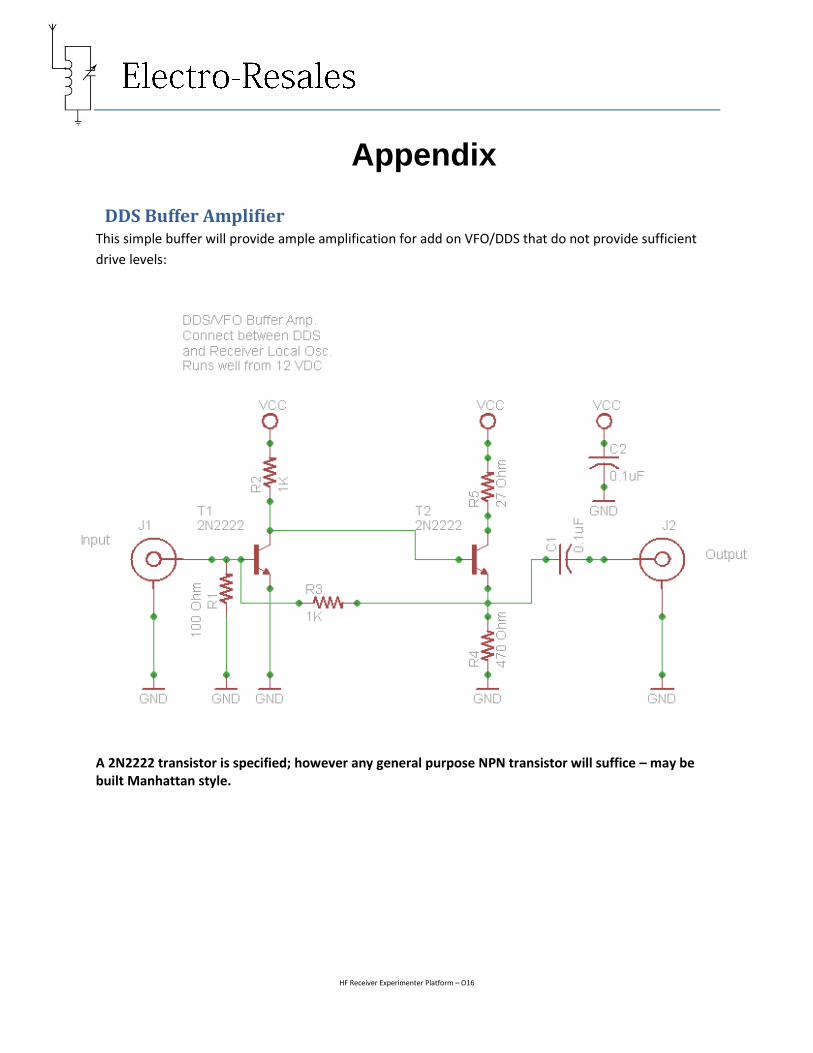
1. Add a local oscillator. As supplied a 10 MHz block oscillator is installed on the board,
however, a vertical SMA socket is also installed, marked LO Inject.
By removing the block oscillator a signal can be injected via this SMA LO Inject socket from a
signal generator or other signal producing device, such as a DDS. This receiver platform has
been tested with several types successfully. The N3ZI DDS2 works well as do the commonly
available AD9850 type DDS from eBay.
It is possible that while the SA602 can be driven directly by the output of the DDS, a small
buffer amplifier may also be needed. This can be a simple 1 or 2 transistor buffer, such as
shown in the appendix.
Using an external oscillator or DDS produces a wideband receiver capable of tuning from
approx. 2 MHz to about 18 MHz
2. Using a tunable AF filter. As supplied the receiver has good audio, however, like many
simple receivers it does lack selectivity. Adding an out board AF filters at the speaker jack is
one possibility or a filter can be added between the SA602 and the LM386. This mod will need
the trace coming from the SA602 pin 4 to be cut and a small gap created to allow the filter to
be inserted. A variety of filter designs exist and have been shown to create a useful
improvement especially when receiving Morse (CW)
3. BCI Filter. One drawback of the direct conversion receiver is that a local or not so local high
power broadcast station can blanket the receiver on all bands and prevent good reception. A
BCI filter at the antenna jack is often a good solution. A simple filter is shown in the appendix
that has proven satisfactory for reducing BCI. Additionally adding a 10uF electrolytic capacitor
on the bottom (trace) side of the PCB between Pin 7 (positive of the electrolytic) and ground
of the LM386 can also help to bypass or reduce this interference.
4. RF Pre-selector. While the receiver has good sensitivity (measured at ) a pre-selector can
help pull out weak signals and in some cases bring in signals on an otherwise dead sounding
band. A variety of circuit options exist for a Pre-selector.
5. Simple Transceiver. A local oscillator can be used to drive both the receiver and a
simple transmitter, to create a transceiver. Some TR switching would be needed of course.
6. Other ideas. This open receiver platform can be the test bed for numerous other
experiments, in particular antenna experiments, and allows the learning by doing principles of
Amateur Radio to be explored in quite a bit of depth. Enjoy and happy experimenting.
HF Receiver Experimenter Platform – O16
Appendix
DDS Buffer Amplifier This simple buffer will provide ample amplification for add on VFO/DDS that do not provide sufficient
drive levels:
A 2N2222 transistor is specified; however any general purpose NPN transistor will suffice – may be built Manhattan style.

HF Receiver Experimenter Platform – O16
BCI Filter The following filter can be fitted at the antenna plug and has been shown to reduce interference.
Filter is best assembled in metal enclosure.

HF Receiver Experimenter Platform – O16
Receiver Schematic

HF Receiver Experimenter Platform – O16
Receiver PCB

HF Receiver Experimenter Platform – O16
Final words & notes
1. Receiver sensitivity was measured with a Wavetek 3001 and was found to be better than 0.1uV.
2. Enclosing the finished PCB in a metal box is recommended, a suitable enclosure is the Hammond 1550M, available form Mouser Electronics as part number 546-1550M.
3. The unpopulated SMA port has a copy of the oscillator frequency present that could be used for driving a digital dial, via a 0.1uF coupling capacitor.
4. For information about WWV : http://www.nist.gov/pml/div688/grp40/wwv.cfm 5. Any questions or comments to; [email protected]

HF Receiver Experimenter Platform – O16
The small Print
DISCLAIMER
Any person who constructs or works on electronic equipment may be exposed to hazards, including physical injury, the risk of electric shock or electrocution.. These hazards can result in health problems, injury, or death. Only qualified persons who understand and are willing to bear these risks themselves should attempt the construction of electronic equipment. By purchasing this item, the buyer acknowledges these risks.
There is a risk of electric shock, electrocution, burns, or fires that is inherent in the construction and use of electronic equipment. By purchasing this item, the buyer acknowledges these risks.
IN NO EVENT SHALL THE SELLER BE LIABLE FOR ANY SPECIAL, INCIDENTAL OR CONSEQUENTIAL DAMAGES OF ANY NATURE including, but not limited to, property damage, personal injury, death or legal expenses. Buyer's recovery from Seller for any claim shall not exceed the purchase price paid by Buyer for the goods, irrespective of the nature of the claim, whether in warrant, contract or otherwise. By purchasing this item, BUYER AGREES TO INDEMNIFY, DEFEND AND HOLD SELLER HARMLESS FROM ANY CLAIMS BROUGHT BY ANY PARTY REGARDING ITEMS SUPPLIED BY SELLER AND INCORPORATED INTO THE BUYER'S PRODUCT.