harley hayden, ed elce, sue ann bidstrup allen, and paul a...
TRANSCRIPT
758 IEEE TRANSACTIONS ON ADVANCED PACKAGING, VOL. 32, NO. 4, NOVEMBER 2009
Adhesion Enhancement Between ElectrolessCopper and Epoxy-based Dielectrics
Harley Hayden, Ed Elce, Sue Ann Bidstrup Allen, and Paul A. Kohl
Abstract—The adhesion between electrolessly deposited copperand an epoxy-containing dielectric material has been investigated.In particular, the role of mechanical anchoring and chemicalbonding in these systems has been examined. The contribution ofeach of these mechanisms to adhesion has been identified. Probelec,a phenolic-novolac epoxy polymer, and Avatrel, an addition poly-merized norbornene polymer with an epoxy side-group, have beentested in this study. Traditional swell and etch treatments havebeen used to enhance mechanical anchoring through pore-typeroughness development on the phenol-novolac epoxy, but werefound to be ineffective in roughening the Avatrel surface. Thecritical difference between the two polymers is the epoxy-back-bone (for the phenolic epoxy) versus the epoxy side-group (for thenorbornene backbone polymer). In order to create roughness onthe Avatrel surface, a novel technique utilizing a blend of Avatreland Probelec was investigated. This technique created pore-typeroughness and enhanced mechanical anchoring on the Avatrelsurface. ��� plasma treatments were utilized to enhance thechemical bonding contribution to adhesion and produce surfaceswith peel strengths of 0.15–0.25 N/mm with minimal roughnessgeneration. Finally, a combined wet-chemical and plasma treat-ment protocol was investigated to enhance chemical bondingand mechanical anchoring on the same surface. Samples withadhesion greater than 0.5 N/mm with roughness less than 50 nmwere produced with both Avatrel and Probelec. Through the useof a combined wet-chemical and plasma-surface treatment thepolymer surface has been optimized for adhesion while minimizingroughness.
Index Terms—Adhesion, dielectric materials, electroless copper,plasma processing.
I. INTRODUCTION
N EW technologies and processes are being developed tomeet the demand for high density interconnects for inte-
grated circuits (ICs). At the board and package level, sequentialbuildup structures (SBUs) and microvias have been integratedinto the manufacture of printed circuit boards (PCBs) as onemeans of achieving high density interconnections. These fea-tures are typically formed on a PCB with alternating dielectricand copper layers. A key to the performance and reliability ofthese SBUs is the adhesion between the deposited copper andthe dielectric materials. Surface roughness causes scattering of
Manuscript received January 14, 2008; revised November 11, 2008. First pub-lished July 21, 2009; current version published November 04, 2009. This workwas recommended for publication by Associate Editor D. Lu upon evaluationof the reviewers comments.
The authors are with the School of Chemical and Biomolecular Engineering,Georgia Institute of Technology, Atlanta, GA 30332 USA.
Color versions of one or more of the figures in this paper are available onlineat http://ieeexplore.ieee.org.
Digital Object Identifier 10.1109/TADVP.2009.2017274
electrons at high frequency; however, roughness improves themechanical anchoring of the metal film. As the feature den-sity and off-chip frequency increase, the average feature sizeshrinks, and the interface between the metal and dielectric ma-terials must become smoother to avoid feature dislocation andsurface scattering. Future dielectric materials must also have im-proved electrical properties, in particular permittivity and loss,in order to enable the smaller features and higher frequencyperformance.
Achieving a smooth metal-dielectric interface is especiallychallenging because the metal-to-dielectric adhesion is achievedthrough a combination of chemical bonding and mechanical an-choring [1]–[3]. Enhancing adhesion while minimizing rough-ness requires advances in chemical bonding and reduced depen-dence on mechanical anchoring. In order to achieve this, it isimportant to identify the individual contributions of each mech-anism to adhesion. In the case of traditional phenolic epoxy ma-terials and electroless copper metallization, it has been shownthat physical anchoring accounts for the majority of adhesion[4], [5]. Improving adhesion with these materials is typicallyachieved through physical modification of the dielectric surface.
This physical modification occurs through a multistep swelland etch process that generates root mean squared roughnessup to 500 nm with peel strengths as large as 1.5 N/mm [6].The development of pore-type roughness on the surface of atraditional epoxy has been well documented in the literature.Siau et al. has postulated a mechanism for pore development inwhich the swelling agent rearranges polar groups in the polymerinto packets and the etch solution then preferentially attacksthese packets forming pores [7], [8]. The schematic in Fig. 1shows the proposed etch mechanism for the epoxy system. Thesite of attack for the etch solution is the ether linkage formedby the opening of the epoxide ring during the curing process.In traditional epoxy materials, this ether linkage is located inthe polymer backbone, allowing the etch reaction to remove asmall segment of the polymer chain and expose the next linkagefor subsequent etch attack. In this manner, the etching processworks down the polymer chain, eventually removing the entirechain and beginning the process of forming pores on the sur-face. This swell and etch process on epoxy materials typicallycreates a surface with pore-type roughness, where the pores canbe micrometers in diameter and depth [3]. It is these large pores,with feature sizes in the range of the skin depth of copper at highfrequencies, which cause electron scattering and signal distor-tion. This effect is increasingly important because the off-chipfrequency is projected to increase by 25% per year for the nextdecade reaching 41 GHz by 2017. This corresponds to a de-crease in copper skin depth from 1000 nm in 2007 to 315 nm
1521-3323/$26.00 © 2009 IEEE
Authorized licensed use limited to: Georgia Institute of Technology. Downloaded on November 13, 2009 at 15:35 from IEEE Xplore. Restrictions apply.

HAYDEN et al.: ADHESION ENHANCEMENT BETWEEN ELECTROLESS COPPER AND EPOXY-BASED DIELECTRICS 759
Fig. 1. Phenol-novolac epoxy etch mechanism schematic.
Fig. 2. (a) Probelec chemical structure. (b) Avatrel chemical structure.
in 2017 [9]. Minimizing the need for large pores is a key toachieving high performance substrates using current materials.
One method for reducing the need for large pores and themechanical anchoring they provide is to increase chemicalbonding, which has the ability to enhance adhesion withoutcreating roughness on the surface [1], [10]–[12]. In order toenhance chemical bonding between a dielectric material andelectroless copper, the concentration of active chemical groupson the surface of the polymer must be increased. Wet-chemicaltreatments such as graft polymerization, coupling agents, andsurface synthesis techniques have been studied by numerousresearchers as means of increasing the content of certain activegroups on the surface [2], [13]–[16]. Plasma treatments havealso been utilized with a variety of materials to activate surfaces[17]–[21]. A common link in many of these studies is the roleof nitrogen containing functionalities on the surface. Thesehave been shown to enhance catalyst adsorption on polymermaterials and to enhance adhesion by as much as 0.5 N/mmin some systems [17], [19]. Although the exact interactionmechanism between electroless copper and these nitrogengroups is unclear, it appears that both nitrogen–palladium andnitrogen–copper complexes are formed on the surfaces, aidingadhesion [14], [22], [23]. Previous work with polyimides hasshown that 5-min 80-W plasma treatments are effec-tive for enabling catalyst adsorption and enhancing adhesionthrough nitrogen incorporation [17]. In this study, similar
plasma treatment conditions have been utilized on polymersurfaces in an attempt to increase nitrogen concentrations andenhance chemical bonding.
The goal of this work is to utilize both chemical and mechan-ical bonding in order to enhance adhesion while minimizingthe necessary surface roughness of the dielectric material. Twomaterial sets have been studied in this investigation, Probelec81/7081 (Huntsman), a traditional phenol-novolac epoxy, andAvatrel 2190P (Promerus LLC) an addition polynorbornene-based epoxy. The chemical structure for each of these mate-rials is given in Fig. 2. Probelec contains epoxy groups in thebackbone of the polymer, while Avatrel is an advanced epoxymaterial that has a polynorbornene backbone with epoxy side-groups used for crosslinking. Although the goal of strong adhe-sion with smooth surfaces for these two materials is the same,the approach and challenges are quite different. With Probelec,a rough, highly adherent interface is readily available throughtraditional surface treatments. The challenge is to minimize sur-face roughness and replace the lost mechanical anchoring withchemical bonding to maintain adhesion. Avatrel is less suscep-tible to the swell and etch process and does not enable electro-less copper plating in the untreated, as-cured state. Hence, thechallenge here is to understand why the material behaves differ-ently during the swell and etch process and to identify suitableprocessing methods for enhancing contributions of mechanicalanchoring and chemical bonding to adhesion.
Authorized licensed use limited to: Georgia Institute of Technology. Downloaded on November 13, 2009 at 15:35 from IEEE Xplore. Restrictions apply.

760 IEEE TRANSACTIONS ON ADVANCED PACKAGING, VOL. 32, NO. 4, NOVEMBER 2009
Fig. 3. Roughness development versus etch treatment time following a 480-s swell treatment for Probelec and Avatrel.
II. EXPERIMENTAL
Probelec 81/7081 from Huntsman International LLC wasspin coated onto a FR-4 substrate board at a spin speed of1500 rpm to yield a 15- -thick film. The Probelec film wassoft-baked at 100 in a box oven under ambient air for30 min, exposed to a dose of 1400 mJ/cm from a 365-nm lightsource (Spectra-Physics model 92521), hard-baked at 100for 60 min, and cured at 145 under ambient air for 55 min.Avatrel 2190 P from Promerus was spin coated onto a siliconwafer at a spin speed of 1500 rpm to yield a 15- -thick film.The Avatrel film was soft-baked at 100 on a hotplate for10 min, exposed to a dose of 200 mJ/cm from a 365-nm lightsource (lamp maker), hard-baked in a box oven at 100 for20 min, and cured in a Lindberg tube furnace under ambientnitrogen at 165 for 60 min. Blends of Avatrel and Probelec(identified as AP henceforth) were prepared with mechanicalmixing (magnetic stir bar) for 24 h and ultrasonic mixing forup to 8 h. The mixtures were then immediately spin-coated at1000 rpm and cured in the same manner as the pure Avatrelmaterial.
Wet-chemical treatments were carried out using three dif-ferent solutions, a swelling solvent (Shipley MLB 211 andCuposit Z) at 80 , a potassium permanganate etch bath(Shipley Circuposit 3308 A and B) at 80 , and a neutralizingbath (Shipley 3314) at room temperature. Plasma treatmentswere carried out in a Unaxis plasma-enhanced chemical vapordeposition (PECVD) chamber. The typical plasma treat-ment parameters were: 20 sccm flow rate, 200 mTorrchamber pressure, 150 substrate temperature, 30–200 W RFpower, and 0.5–5 min treatment times. Following wet chemicalor plasma treatments, the samples were activated with a Sn/Pdcatalyst (Shipley Cataposit 44) at 46 for 20 min. Finally,the samples were plated with 1 of electrolessly depositedcopper (Shipley Circuposit 3350 chemistry) at 46 . Thecopper thickness was increased to 40 for the peel teststhrough electroplating. Additionally, samples were annealed at150 for 1 h following both the electroless and electroplatingcopper deposition steps.
The effect of these treatments was monitored by four ana-lytical techniques. The adhesion strength of the copper to thepolymer was measured with a 90 peel test using an Instron(Model 5842) instrument following the ASTM B 533-85 stan-dard [24]. In this test, a 10-mm-wide strip of copper was pulledat the rate of 25 mm/min and the average force was calculatedand divided by the peel strip width to yield the peel strength in
N/mm. Analysis of the chemical state of the surface was per-formed with a Perkin Elmer XPS system (Model PHI 1600). AMolecular Imaging Picoplus AFM in the tapping mode was uti-lized to quantify the root mean square (rms) roughness of thesurface and for qualitative analysis of the morphology of thatroughness. The AFM tip diameter was less than 10 nm. Finally,a scanning electron microscope (SEM) (Zeiss SEM Ultra 60)was utilized to analyze the morphology of the polymer surfaces.
III. RESULTS
Roughness formation on Probelec and Avatrel surfacesfollowing a swell and etch treatment is quantified in Fig. 3.RMS roughness values for Probelec increase with increasingetch treatment times, reaching a maximum of 800 nm withextended etching. Traditional treatment conditions of a 480-sswell and a 600-s etch produce rms roughness of 400 nmwith corresponding adhesion of up to 1.5 N/mm. The surfaceroughness that forms in Avatrel, however, is more than an orderof magnitude less than with Probelec, with a maximum rmsroughness development of 35 nm. These treatment conditionsproduced no measurable adhesion between Avatrel and elec-troless copper. The roughness morphology also depends onthe kind of material (Fig. 4). The Probelec surface develops apore-type roughness forming large, deep pores with extendedetching times. The Avatrel surface, however, does not exhibitpore-type roughness formation. Instead, surface roughnessincreases are realized in the form of peak-valley structures,which are uniform across the surface.
In order to form pore-type roughness on a surface containingAvatrel, AP mixtures were used. Fig. 5 shows the resulting sur-faces when these mixtures are exposed to a 2000-s swell and2000-s etch treatment. Fig. 5(a) shows a sample with 5% Prob-elec in the mixture. Only one pore can be seen in this 100-scan after the swell and etch process. Fig. 5(b) is for the 10%Probelec sample, which shows the presence of approximately30 pores in the 100- scan. Fig. 5(c) is for a sample with 20%Probelec yielding 40 pores in the 100- scan. In each case,the pores are of the same approximate size, 200–500-nm-di-ameter and are evenly dispersed across the polymer surface.Changing the concentration of Probelec in the mixture affectspore concentration and not pore size or depth. Fig. 5(d) is a 3-DAFM image of the 20% Probelec sample illustrating that thepores formed on the surface are a maximum of 65 nm deep.
Mechanical and ultrasonic mixing techniques were studiedwith the 20% Probelec AP mixture in order to understand the
Authorized licensed use limited to: Georgia Institute of Technology. Downloaded on November 13, 2009 at 15:35 from IEEE Xplore. Restrictions apply.

HAYDEN et al.: ADHESION ENHANCEMENT BETWEEN ELECTROLESS COPPER AND EPOXY-BASED DIELECTRICS 761
Fig. 4. AFM images of (a) Probelec and (b) Avatrel following a swell and etch treatment.
Fig. 5. AFM scans of Avatrel/Probelec mixture surface following 2000-s swell and 2000-s etch treatment: (a) 5% Probelec, (b) 10% Probelec, (c) 20% Probelec,(d) 20% Probelec 3-D image.
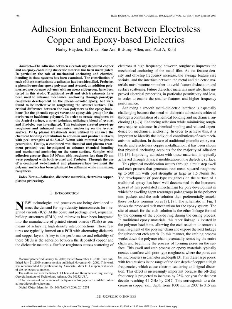
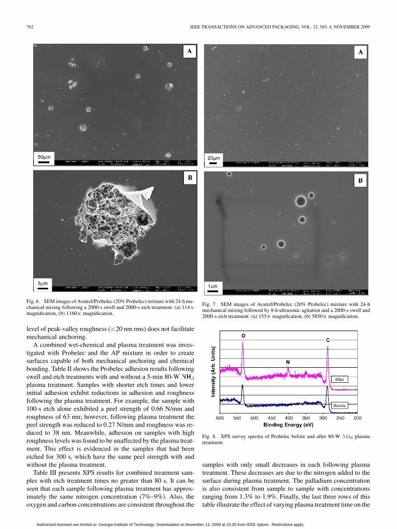
effect on pore size and distribution. Fig. 6 presents two SEMimages of the polymer surface following 24 h of mechanicalmixing and a 2000-s swell and 2000-s etch treatment. Thesmooth, dark field in these images is the Avatrel material,which is largely unaffected by the swell and etch process.The lighter areas are Probelec regions that have been etchedto create roughness. It can be seen in Fig. 6(a) that there aremany large Probelec particles, up to 50 in diameter, stillpresent following purely mechanical mixing. Fig. 6(b) is ahigher magnification image of one of these particles that showsthe rough features created when large areas of Probelec areleft in the mixture. AFM images indicate that in additionto these large Probelec areas, there are also well dispersed,smaller particles as evidenced by the small pores seen in Fig. 5.Fig. 7 shows SEM images of a solution that was mechanicallymixed for 24 h and then subjected to ultrasonic agitation fora further 8 h. Fig. 7(a) shows a wide field SEM image withProbelec features as large as 10 . The majority of thissurface contains very small features, as shown in Fig. 7(b), witha diameter of 200–500 nm. AFM scans confirm the presenceof well-dispersed 200–500-nm Probelec areas on the surface.Thus ultrasonic mixing breaks up the largest Probelec particles,creating more uniformly sized pores on the surface. Despitethese advances in roughness development, the surfaces of the
AP mixture did not enable catalyst adsorption or electrolesscopper deposition without further treatment. Thus, the role ofpurely mechanical bonding could not be quantified using thisapproach alone.
plasma treatments were utilized to enhance catalystadsorption and chemical bonding on the polymer surfaces.Fig. 8 presents two XPS survey scans for Probelec, beforeand after plasma treatment. Before plasma treatment, the Pro-belec shows the presence of two elements, carbon (73.2%)and oxygen (26.8%). Following plasma treatment, the surfacecontains three elements, carbon (68.7%), oxygen (23.3%), andnitrogen (8.0%). Fig. 9 shows XPS survey scans for Avatrel.As with Probelec, there are two elements on the surface be-fore plasma treatment, carbon (91.9%) and oxygen (8.1%),and three present after the plasma, carbon (72.8%) oxygen(22.1%), and nitrogen (5.1%). These plasma treatments alsoincreased adhesion with the electroless copper. The Probelecpeel strength increased from 0 to 0.11 N/mm, and the Avatrelpeel strength increased from 0 to 0.26 N/mm. In both cases, therms roughness of the surface remained below 20 nm followingplasma treatments. Increasing plasma power was found tocreate less chemical modification and more roughness on theAvatrel surface (Table I). These conditions enabled plating butdid not create any measurable adhesion, indicating that this
Authorized licensed use limited to: Georgia Institute of Technology. Downloaded on November 13, 2009 at 15:35 from IEEE Xplore. Restrictions apply.
762 IEEE TRANSACTIONS ON ADVANCED PACKAGING, VOL. 32, NO. 4, NOVEMBER 2009
Fig. 6. SEM images of Avatrel/Probelec (20% Probelec) mixture with 24-h me-chanical mixing following a 2000-s swell and 2000-s etch treatment: (a) 114�magnification, (b) 1160� magnification.
level of peak-valley roughness ( 20 nm rms) does not facilitatemechanical anchoring.
A combined wet-chemical and plasma treatment was inves-tigated with Probelec and the AP mixture in order to createsurfaces capable of both mechanical anchoring and chemicalbonding. Table II shows the Probelec adhesion results followingswell and etch treatments with and without a 5-min 80-Wplasma treatment. Samples with shorter etch times and lowerinitial adhesion exhibit reductions in adhesion and roughnessfollowing the plasma treatment. For example, the sample with100-s etch alone exhibited a peel strength of 0.66 N/mm androughness of 63 nm; however, following plasma treatment thepeel strength was reduced to 0.27 N/mm and roughness was re-duced to 38 nm. Meanwhile, adhesion on samples with highroughness levels was found to be unaffected by the plasma treat-ment. This effect is evidenced in the samples that had beenetched for 300 s, which have the same peel strength with andwithout the plasma treatment.
Table III presents XPS results for combined treatment sam-ples with etch treatment times no greater than 80 s. It can beseen that each sample following plasma treatment has approx-imately the same nitrogen concentration (7%–9%). Also, theoxygen and carbon concentrations are consistent throughout the
Fig. 7. SEM images of Avatrel/Probelec (20% Probelec) mixture with 24-hmechanical mixing followed by 8-h ultrasonic agitation and a 2000-s swell and2000-s etch treatment: (a) 155� magnification, (b) 5850� magnification.
Fig. 8. XPS survey spectra of Probelec before and after 80-W �� plasmatreatment.
samples with only small decreases in each following plasmatreatment. These decreases are due to the nitrogen added to thesurface during plasma treatment. The palladium concentrationis also consistent from sample to sample with concentrationsranging from 1.3% to 1.9%. Finally, the last three rows of thistable illustrate the effect of varying plasma treatment time on the
Authorized licensed use limited to: Georgia Institute of Technology. Downloaded on November 13, 2009 at 15:35 from IEEE Xplore. Restrictions apply.

HAYDEN et al.: ADHESION ENHANCEMENT BETWEEN ELECTROLESS COPPER AND EPOXY-BASED DIELECTRICS 763
TABLE IPEEL STRENGTH, RMS ROUGHNESS, AND XPS RESULTS FOR AVATREL AND AP MIXTURES
TABLE IIPEEL STRENGTHS AND RMS ROUGHNESS VALUES FOR PROBELEC WITH AND WITHOUT
PLASMA TREATMENT (ALL SAMPLES RECEIVED A 30-s SWELL TREATMENT)
Fig. 9. XPS survey spectra of Avatrel before and after 80-W �� plasmatreatment.
surface concentrations of nitrogen. It can be seen that reducingthe treatment time from 5 min to 30 s reduces nitrogen concen-tration from 9.6% to 8.9%.
Fig. 10 shows the peel test results for Probelec with a swelland etch only treatment and with a combined swell, etch, andplasma treatment. In the swell and etch only data set samplesreceived a 30-s swell treatment and a 30–100-s etch treatment.Roughness under these conditions remained below 100 nm in allcases with adhesion ranging from 0.4 to 0.65 N/mm. The com-bined treatment data set used the same range of swell and etchconditions, with an additional 30-s 80-W plasma treat-ment. These treatments created improved adhesion when com-pared to the swell and etch only surface. The offset between thedata sets was approximately 0.20 N/mm for a given rms rough-ness value. Adhesion between electroless copper and Avatrelmaterials was also measured. Utilizing the 20% Probelec APmixture with a 2000-s swell, 2000-s etch, and a 30-s 80-W
treatment peel strength increased to 0.51 N/mm with rmsroughness values less than 20 nm (Table I). This peel strength
is 0.25 N/mm larger than that obtained with purely chemicalbonding from plasma treatments alone.
IV. DISCUSSION
In order to increase adhesion while maintaining smooth sur-faces, processes that combine chemical bonding and mechan-ical anchoring have been investigated. An attempt was made toquantify the contributions of each mechanism through experi-mentation, with wet-chemical treatments used for mechanicalanchoring improvements and plasma treatments for chemicalbonding enhancement. The individual contributions to adhesionhave been combined to produce optimum surfaces with the min-imum necessary roughness and acceptable adhesion.
When comparing the degree of roughness created in Prob-elec and Avatrel by wet etching it is apparent that different pro-cesses are occurring, producing roughness with different mag-nitudes and morphologies from one material to the other. TheProbelec pore-type roughness formation described in the in-troduction does not occur in Avatrel because of the locationand function of the epoxy groups. In Avatrel, unlike Probelec,the epoxy groups are present as side-groups off of the mainpolymer chain and are mainly responsible for crosslinking of thepolymer. Upon curing, approximately 80% of the epoxide ringsare opened and used for crosslinking, producing a series of etherlinkages connecting polymer chains [25]. The Avatrel materialused in this study, which has a molecular weight of 200 000a.m.u. contains approximately 200 epoxy-related crosslinks perpolymer chain when cured. When the etch process attacks oneof the ether linkages on these crosslinks, it enables the attackof subsequent linkages on the same crosslink chain (Fig. 11).Once all the ether linkages on a given crosslink are etched thereis no mechanism for propagation of the etch process into themain polymer chain and it stops. Etching of the maximum lengthof polymer side group leads to the loss of the equivalent of an
Authorized licensed use limited to: Georgia Institute of Technology. Downloaded on November 13, 2009 at 15:35 from IEEE Xplore. Restrictions apply.

764 IEEE TRANSACTIONS ON ADVANCED PACKAGING, VOL. 32, NO. 4, NOVEMBER 2009
TABLE IIIDETAILED PROBELEC XPS RESULTS (ALL SAMPLES RECEIVED A 30-s SWELL TREATMENT)
Fig. 10. Peel strength versus RMS roughness chart for Probelec samples with and without 30-s 80-W �� plasma treatments.
eight carbon chain with an approximate length of just 1.2 nm,as opposed to Probelec in which the entire polymer chain canbe removed in an etching sequence. Removing repeated smalllengths of polymer through extending etching leads to the re-tention of relatively smooth surfaces with only the peak-valleyroughness morphology seen in Fig. 4.
This work illustrates that the epoxy functionality alone isnot sufficient for creating high levels of pore-type roughness. Ifthis functionality is present in the polymer backbone it enablespore-formation roughness and enhanced adhesion. Moving thisfunctionality to a side group off of the main polymer chain, how-ever, minimizes the effect of the etch process leaving materialssmooth and providing no adhesion enhancement. It is clear thatin order to enhance adhesion with advanced materials differenttechniques are required. A new approach (i.e., using a blendof Avatrel and Probelec) has been taken to form the pore-typeroughness needed for mechanical interlocking on the Avatrelsurface.
In this approach, a small amount (5%–20% by weight) ofProbelec in propylene glycol methyl ether acetate (PGMEA)is mixed with Avatrel in mesitylene. The solvents for thesepolymers are immiscible leading to the formation of twophases in the mixture, with small droplets of Probelec/PGMEAsuspended in the Avatrel/mesitylene bulk phase. Ideally thesedroplets would be small and uniformly dispersed throughoutthe bulk phase. A process flow diagram for this approach is
shown in Fig. 12. After the mixing, spin-coating, and curingprocesses described in the experimental procedures sectionof this report, the AP blend is subjected to a swell and etchtreatment that preferentially etches the Probelec areas whileleaving the Avatrel areas smooth. The Probelec droplets canbe thought of as space-holders which are removed through theetch process to leave pores on the Avatrel surface. The resultingsurface contains well-dispersed pores that are 200–500 nmin diameter and 70 nm deep, as shown in Fig. 5. The rmsroughness of these surfaces remains low, less than 20 nm,despite the presence of pores because the Avatrel surface islargely unaffected by the etch process. The uniformity of thesesurfaces and the dispersion of pores is strongly affected by themixing technique used.
Mechanical mixing alone, as shown in Fig. 6, does not ad-equately break-up large Probelec particles, leaving 30–50areas of Probelec on the surface. When these large particles aresubjected to the swell and etch process they act like the Prob-elec bulk material, creating large scale pores and extreme rough-ness. Probelec particles in the 200–500-nm-diameter range areremoved completely by the etch process, leaving the same sizepore on the surface. The larger particles however, are not com-pletely removed leaving the large pores and high levels of rough-ness seen in Fig. 6. This leads to inconsistent adhesion, highadhesion over these Probelec areas and normal adhesion else-where, and large variance in roughness across the polymer sur-
Authorized licensed use limited to: Georgia Institute of Technology. Downloaded on November 13, 2009 at 15:35 from IEEE Xplore. Restrictions apply.

HAYDEN et al.: ADHESION ENHANCEMENT BETWEEN ELECTROLESS COPPER AND EPOXY-BASED DIELECTRICS 765
Fig. 11. Avatrel etch mechanism schematic.
face, leading to electrical performance and mechanical relia-bility issues. Adding ultrasonic mixing to the process enablesthe breakup of more of these large particles, leaving the surfacemore uniform (Figs. 5 and 7) and minimizing the problems ofinconsistent adhesion and roughness across the surface [26].
Plasma treatments were studied in order to enable catalystadsorption and improve adhesion through improved chemicalbonding. These treatments on Probelec and Avatrel are shown toincrease adhesion by 0.15 and 0.26 N/mm, respectively, whilemaintaining smooth surfaces. The level of surface roughnesscreated in this process (17 nm for Probelec, 9.4 nm for Avatrel)is quite low. Avatrel materials with similar roughness (16.3 nm)obtained through higher power plasma treatments have shownno adhesion, indicating that this level of peak-valley rough-
ness does not enable mechanical anchoring (Table I). Thus,the adhesion gains realized through these plasma treatments(0.15–0.26 N/mm) can be attributed to chemical bondingimprovements on the polymer surface.
Combined treatments, which take advantage of both me-chanical anchoring and chemical bonding, were attempted withProbelec and the AP mixture, utilizing the optimum conditionsidentified in the individual investigations. It was found thatthe optimum conditions for mechanical anchoring, long swelland etch treatments and rough surfaces, were not suitablefor combined treatments. These conditions produced surfaceswith more roughness than desired and led to cohesive failureinside the polymer, not adhesive failure at the copper/polymerinterface. The effect of plasma treatment which enhances
Authorized licensed use limited to: Georgia Institute of Technology. Downloaded on November 13, 2009 at 15:35 from IEEE Xplore. Restrictions apply.

766 IEEE TRANSACTIONS ON ADVANCED PACKAGING, VOL. 32, NO. 4, NOVEMBER 2009
Fig. 12. Avatrel/Probelec mixture process flow diagram.
adhesion at the interface is not measured when failure occurscohesively (Table II, 300- and 600-s etch data). In order toquantify the effect of these treatments, adhesion must occuradhesively at the interface. Limiting the swell to 30 s andthe etch 30-100 s produced samples that failed adhesivelywith and without plasma treatments, while maintaining rmsroughness levels below 100 nm. Utilizing these conditions witha 5-min 80-W plasma treatment following the swell andetch proved to reduce adhesion compared to the samples withswell and etch alone (Table II, 50 and 100 s etch data). The5 min plasma treatment significantly decreases the roughnessof the surface (up to 41 nm rms roughness reduction) throughplasma etching, reducing mechanical anchoring and adhesion.Limiting the plasma time to 30 s, thereby reducing the timeof plasma etching, minimized the smoothing effect whilemaintaining the desired chemical modifications of the surface.Table III confirms the plasma treatment creates similarchemical modifications whether treatment time is 30 s, 2 min,or 5 min treatment times as evidenced by consistent nitrogenconcentration increases on the surface.
Utilizing a 30-s swell, 30–100-s etch, and 30-s 80-Wplasma condition, combined treatments were tested. Fig. 10compares peel test results with and without the plasma treat-ment. With a purely swell and etch treatment Probelec exhibitspeel strength values between 0.38 and 0.65 N/mm depending onthe roughness generated. These peel strength values correspondto the contribution of mechanical anchoring on the surface.Adding the plasma treatment increases adhesion for a givenlevel of rms roughness. The difference in adhesion before and
after plasma treatments for a given rms value is a measureof the contribution of chemical bonding to adhesion. In theseexperiments this contribution was consistently 0.20 N/mm.Thus, this technique is capable of combining the effects ofchemical bonding and mechanical anchoring and allowing forthe quantification of the contributions of each to adhesion. Theresulting surfaces are smooth and adherent, with rms roughnessas low as 40 nm and peel strength values over 0.5 N/mm formost samples. The same effect was also realized with the APmixtures, improving adhesion from 0.26 N/mm with plasmaonly treatments to 0.51 N/mm with combined treatments(Table I). In this case the 0.26 N/mm corresponds to chemicalbonding and the remainder, 0.25 N/mm, is due to enhancedmechanical anchoring contributed by the pores formed on thesurface.
V. CONCLUSION
A study of adhesion between epoxy-containing substratesand electrolessly deposited copper has been presented. In thisstudy the contributions of mechanical anchoring and chemicalbonding were measured individually in order to determinetheir relative magnitudes and suitable conditions for producingoptimum surfaces. For the first time, a study of the etch processfor materials with epoxy functionalities as side-groups off ofthe main polymer chain has been presented. A mechanism forthis process with Avatrel has been postulated and comparedwith the process for a traditional dielectric material with epoxyin the polymer backbone. Wet-chemical and plasma treatmentswhich provide optimum mechanical anchoring and chemicalbonding respectively have been identified. Following this work,a treatment protocol that allows both mechanical anchoring andchemical bonding to contribute to adhesion on the same samplewas identified. These conditions produced adhesion of greaterthan 0.5 N/mm for samples with rms roughness less than 50 nmon the surface by combining the benefits of chemical bondingand mechanical anchoring on one surface. These results aid theprocess of maintaining adequate adhesion on smooth surfacesfor use with future microelectronic applications.
REFERENCES
[1] A. Ahagon and A. N. Gent, J. Polymer Sci. Part B—Polymer Phys., vol.13, pp. 1285–1300, 1975.
[2] M. B. Chan-Park and S. S. Tan, Int. J. Adhesion Adhesives, vol. 22, pp.471–475, 2002.
[3] J. Ge, R. Tuominen, and J. K. Kivilahti, J. Adhesion Sci. Technol., vol.15, pp. 1133–1143, 2001.
[4] J. Ge, M. Turunen, and J. Kivilahti, Thin Solid Films, vol. 440, pp.198–207, 2003.
[5] D. Schroer, R. J. Nichols, and H. Meyer, Electrochimica Acta, vol. 40,pp. 1487–1494, 1995.
[6] S. Siau, A. Vervaet, L. Van Vaeck, E. Schacht, U. Demeter, and A. VanCalster, J. Electrochem. Soc., vol. 152, pp. C442–C455, 2005.
[7] S. Siau, A. Vervaet, S. Nalines, E. Schacht, and A. Van Calster, J. Elec-trochem. Soc., vol. 151, pp. C816–C830, 2004.
[8] S. Siau, A. Vervaet, S. Nalines, E. Schacht, and A. Van Calster, J. Elec-trochem. Soc., vol. 151, pp. C831–C849, 2004.
[9] International Technology Roadmap for Semiconductors 2006 [Online].Available: http://public.itrs.net/
[10] W. Dressick, C. Dulcey, J. Georger, G. Calabrese, and J. Calvert, J.Electrochem. Soc., vol. 141, pp. 210–220, 1994.
[11] F. M. Fowkes, Indust. Eng. Chem., vol. 56, p. 40, 1964.[12] A. N. Gent and S. M. Lai, J. Polymer Sci. Part B—Polymer Phys., vol.
32, pp. 1543–1555, 1994.
Authorized licensed use limited to: Georgia Institute of Technology. Downloaded on November 13, 2009 at 15:35 from IEEE Xplore. Restrictions apply.

HAYDEN et al.: ADHESION ENHANCEMENT BETWEEN ELECTROLESS COPPER AND EPOXY-BASED DIELECTRICS 767
[13] M. Charbonnier, Y. Goepfert, M. Romand, and D. Leonard, J. Adhe-sion, vol. 80, pp. 1103–1130, 2004.
[14] M. S. Chen, S. L. Brandow, C. S. Dulcey, W. J. Dressick, G. N. Taylor,J. F. Bohland, J. H. G. Georger, E. K. Pavelchek, and J. M. Calvert, J.Electrochem. Soc., vol. 146, pp. 1421–1430, 1999.
[15] Y. J. Chen, E. T. Kang, K. G. Neoh, and W. Huang, Langmuir, vol. 17,pp. 7425–7432, 2001.
[16] Z. Yu, E. Kang, and K. Neoh, Polymer, vol. 43, pp. 4137–4146, 2002.[17] D. Bhusari, H. Hayden, R. Tanikella, S. A. B. Allen, and P. A. Kohl, J.
Electrochem. Soc., vol. 152, pp. F162–F170, 2005.[18] J. F. Friedrich, R. Mix, and G. Kuhn, Surface Coatings Technol., vol.
174, pp. 811–815, 2003.[19] J. F. Friedrich, R. Mix, and G. Kuhn, Surface Coatings Technol., vol.
200, pp. 565–568, 2005.[20] S. K. Koh, S. C. Park, S. R. Kim, W. K. Choi, H. J. Jung, and K. D.
Pae, J. Appl. Polymer Sci., vol. 64, pp. 1913–1921, 1997.[21] C. Y. Yang, J. S. Chen, and S. L. C. Hsu, J. Electrochem. Soc., vol. 153,
pp. F120–F125, 2006.[22] S. Siau, A. Vervaet, E. Schacht, U. Demeter, and A. Van Calster, Thin
Solid Films, vol. 495, pp. 348–356, 2006.[23] W. H. Yu, E. T. Kang, and K. G. Neoh, J. Electrochem. Soc., vol. 149,
pp. C592–C599, 2002.[24] , ASTM B Standard 533-85, 2002.[25] P. Chiniwalla, Y. Q. Bai, E. Elce, R. Shick, W. C. McDougall, S. A.
B. Allen, and P. A. Kohl, J. Appl. Polymer Sci., vol. 89, pp. 568–577,2003.
[26] J. G. Ryu, H. Kim, and J. W. Lee, Polymer Eng. Sci., vol. 44, pp.1198–1204, 2004.
Harley Hayden received the B.S. degree from Johns Hopkins University,Baltimore, MD, in 2002, and the Ph.D. degree from the Georgia Institute ofTechnology, Atlanta, in 2008, both in chemical engineering.
He is currently a Postdoctoral Research Fellow at the Georgia Institute ofTechnology working towards the fabrication of multiplexed single-ion ion trapsfor quantum computing applications. His research interests include microelec-tronics fabrication, advanced computing, and alternative energy solutions.
Ed Elce, photograph and biography not available at the time of publication.
Sue Ann Bidstrup Allen received the S.B. degreefrom the Massachusetts Institute of Technology(MIT), Cambridge, MA, and the Ph.D. degreein chemical engineering from the University ofMinnesota, Minneapolis.
She is currently a Professor with the School ofChemical and Biomolecular Engineering, GeorgiaInstitute of Technology (Georgia Tech), Atlanta.Prior to her appointment at Georgia Tech, she andspent two years as a Postdoctoral Associate withthe Electrical Engineering Department, MIT. Her
research interests intersect the areas of polymer engineering, microelectronicmaterials, and processing.
Dr. Bidstrup Allen received the National Science Foundation PresidentialYoung Investigator Award, the DuPont Young Faculty Award, and the GeorgiaTech Faculty Leadership Award. She is a Fellow of the Society of PlasticEngineers.
Paul A. Kohl received the Ph.D. degree from the Uni-versity of Texas, Austin, in 1978.
He is currently a Regents’ Professor and holder ofthe Hercules Inc./Thomas L. Gossage Chair at theGeorgia Institute of Technology. He was employedby AT&T Bell Laboratories, Murray Hill, NJ. In 1989he joined the faculty of Georgia Tech. His researchinterests include new electronic materials and energyconversion technologies. He is the Director of the In-terconnect Focus Center, which is one of the SRC/DARPA s FCRP.
Authorized licensed use limited to: Georgia Institute of Technology. Downloaded on November 13, 2009 at 15:35 from IEEE Xplore. Restrictions apply.