handout 2 for ee-203 bipolar junction transistor …handout 2 for ee-203 bipolar junction transistor...
TRANSCRIPT
Handout 2 for EE-203
Bipolar Junction Transistor (BJT)
Sheikh Sharif Iqbal
(Ref: Text book and KFUPM Online course of EE-203)
(Remember to solve all the related examples, exercises problems as given in the Syllabus)
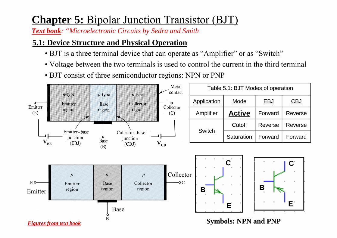
Chapter 5: Bipolar Junction Transistor (BJT)
Saturation
Cutoff
Active
Mode
Table 5.1: BJT Modes of operation
ForwardForward
ReverseReverseSwitch
ReverseForwardAmplifier
CBJEBJApplication
VBE VCB
C
B
E
C
B
E
Symbols: NPN and PNP
Emitter
Collector
Base
Text book: “Microelectronic Circuits by Sedra and Smith
5.1: Device Structure and Physical Operation• BJT is a three terminal device that can operate as “Amplifier” or as “Switch”• Voltage between the two terminals is used to control the current in the third terminal• BJT consist of three semiconductor regions: NPN or PNP
Figures from text book
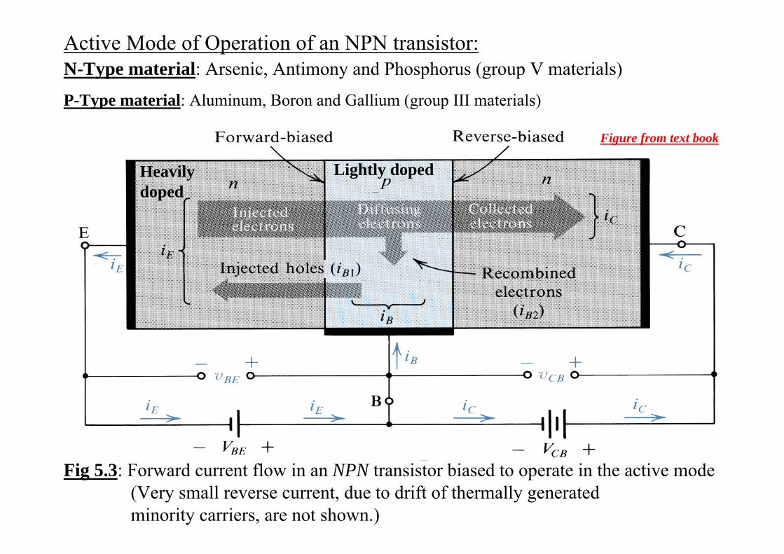
Fig 5.3: Forward current flow in an NPN transistor biased to operate in the active mode (Very small reverse current, due to drift of thermally generatedminority carriers, are not shown.)
Active Mode of Operation of an NPN transistor:
Lightly dopedHeavily doped
N-Type material: Arsenic, Antimony and Phosphorus (group V materials)
P-Type material: Aluminum, Boron and Gallium (group III materials)
Figure from text book
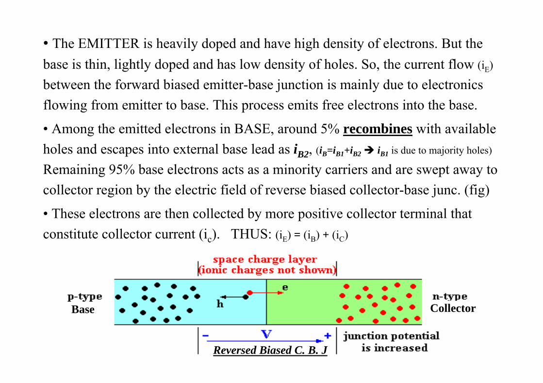
• The EMITTER is heavily doped and have high density of electrons. But the base is thin, lightly doped and has low density of holes. So, the current flow (iE)
between the forward biased emitter-base junction is mainly due to electronics flowing from emitter to base. This process emits free electrons into the base.
• Among the emitted electrons in BASE, around 5% recombines with available holes and escapes into external base lead as iB2, (iB=iB1+iB2 iB1 is due to majority holes)
Remaining 95% base electrons acts as a minority carriers and are swept away to collector region by the electric field of reverse biased collector-base junc. (fig)
• These electrons are then collected by more positive collector terminal that constitute collector current (ic). THUS: (iE) = (iB) + (iC)
Base Collector
Reversed Biased C. B. J

The Collector Current (iC): Base Current (iB):
i C I S e
v BE
V T⋅ i B
i Cβ
I Sβ
e
v BE
V T⋅
Emitter Current (iE):
iE = iC + iB
• Here, n = 1; Saturation current, 10-12> IS>10-14 A and thermal voltage, VT = 25 mV • Note that ‘iC’ is independent of VCB , for VCB ≥0. So collector behaves as an
ideal constant current source where the current is determined by VBE. (fig 2nd slide)
• Since, iC = αiE ; iC = βiB and α= β/(β+1), where “β” is common emitter current gain constant for a particular BJT
“α” is common base current gain
iE iC iB+β 1+
βiC⋅
β 1+
βIS e
vBE
VT⋅
⎛⎜⎜⎝
⎞
⎠⋅ iC α IE⋅ αβ
β 1+
• So the Emitter Current is given by:Exercise BJT-1: For an NPN transistor having Is=10-11 A, β=100 &VT=25mV(at room temperature)
Calculate VBE for iC=1.5A
(Solution: 0.643 V)

Note that the PNP transistors have VEB ; whereas the NPN transistors has VBE
The PNP Transistor operation in Active mode:
Figure from text book


5.2.3: Dependence of current, voltage, temperature and the Early Effect:
0.7v
Exercise BJT-2: If a BJT has VA=100v and IC=1mA, find r0
5.4: How to solve NPN or PNP BJT-DC circuits
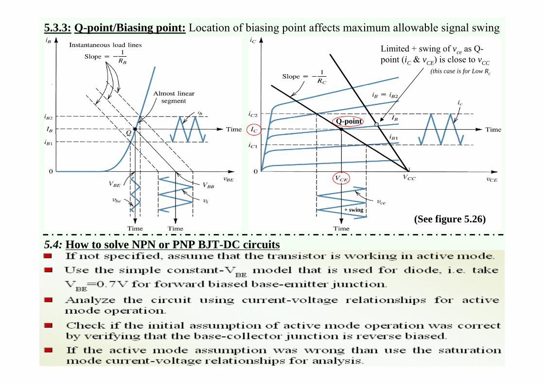
5.3.3: Q-point/Biasing point: Location of biasing point affects maximum allowable signal swing
Limited + swing of vce as Q-point (iC & vCE) is close to vCC
(this case is for Low Rc
Q-point
+ swing
(See figure 5.26)

Assume Active mode
=0.7v
CBJ RB EBJ FB
n
np
Solution:

- Assume Active Mode of operation VBE=0.7
n
n
p
- Since CBJ is RB, - Initial assumption was correct
Solveexamples 5.4 to 5.12

5.5: Biasing single stage BJT Amplifiers: - Operating point or Q-point (iC and vCE)
4.75v
Voltage Divider Biasing
Assume Active mode
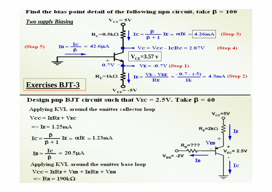
Two supply Biasing
Exercises BJT-3
VCE=3.57 v

Solve example 5.13 & related exercises
Exercises BJT-3:
Exercises BJT-4:

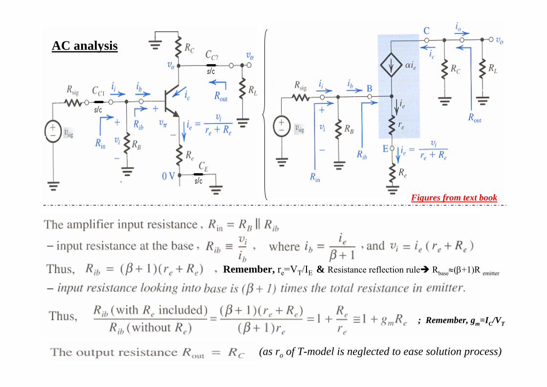
5.6: BJT Amplifiers, Small-Signal Operation and Models :
DCequivalent circuit
ACequivalent circuit
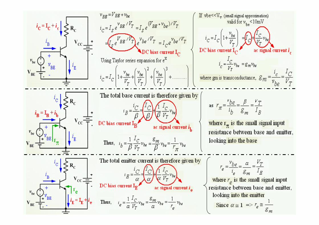

5.6.6 and 5.6.7: Small-Signal Equivalent Circuit Models:
Two different versions of simplified hybrid-Π model for the small-signal operation of the BJT. (a) represents the BJT as a voltage-controlled current source ( a transconductance amplifier) (b) represents the BJT as a current-controlled current source (a current amplifier).
(b)(a)
Two slightly different versions of what is known as the T model of the BJT. The circuit in (a) is a voltage-controlled current source representation and that in (b) is a current-controlled current source representation. These models explicitly show the emitter resistance re rather than the base resistance rΠ featured in the hybrid-π model.
(a) (b)
Solve example 5.14Figures from text book

Lets assume the BJT is operating in Active Mode. Thus,
Since IE = I mA ; IB = IE / (β+1) mA ; VB = 0 - IB.RB ; VE = VB - 0.7 ;
Now IC= α.IE = (β.IE) / (β+1) ; VC = VCC - IC.RC and if CBJ remains RB then assumption is OK
5.7.3:Common emitter Amplifier: DC analysis to find IB, IC, IE, VB, VC and VE
Exercise-5: Find the operating point if VCC=VEE=10V, RC=8 kΩ, RB=100 kΩ, I=1mA & β=100Solution: Q or operating point is, IC=0.99 mA ; VCE=0.3 v (as VB= -1v, VC = 2v, VE = -1.7v)
IB
IC
IE
βVB
VC
VE
IC= α.IE , IC= β.IB and α=β/(β+1)

5.7.3:Common emitter Amplifier: AC analysis to find Gain, Input & output Impedances
Exercise-6: Find Rin ,Rout ,Av & Gv; if Rsig=RL=5kΩ, RB=100k, RC=8k; IC=1mA, IB=0.01mA, VA=100V, VT=25mV
Solution: Ri=2.43 kΩ; Rout=7.4 kΩ, Av=-119 V/V, Gv=-39 V/V (as rπ=2.5K, gm=40 mA/V, r0=100k)
Remember, r0=|VA|/IC
gm=IC/VT
rπ=VT/IB
Figure from text book

Exercises-7:
DC analysis: O/C capacitors & find IB, IC, IE, VB, VC, VE
Find model parameters (rπ, re, gm)
- S/C DC voltage source- O/C DC current source
AC analysis: S/C capacitors& find Rin, Rout, AV, Ai
Review of CE amp:

IB
IC
IE
β
Exercises-8:
5.7.4:Common emitter Amplifier with Re (emitter resistor): Controlled voltage amp
IC= α.IE , IC= β.IB α=β/(β+1)
DC analysis
Exercise-9: Find the operating point if VCC=VEE=10V, RC=8 kΩ, RB=100 kΩ, I=1mA & β=100Solution: operating point, IC=0.99 mA ; VCE=3.7 v (as IE=1mA ; VB= -1v, VC = 2v, VE = -1.7v)
andgm=IC/VT; re=VT/IE ;
AC analysis
Remember, re=VT/IE & Resistance reflection rule Rbase≈(β+1)R emitter
(as ro of T-model is neglected to ease solution process)
; Remember, gm=IC/VT
Figures from text book

5.7.3:Common Emitter (CE) with Emitter Resistance (Re): AC analysis (cont’d…)
Exercise-10: if IE=1mA, IC=0.99mA, Re=225Ω, RB=100kΩ, RC=8kΩ, Rsig=RL=5kΩ, β=100, VT=25mV,
Neglect ro to FIND Rin , Rout , Av,, Gv Sol: Ri=20.16 kΩ; Rout=8 kΩ, Av= -12.18V/V, Gv=-9.76v/v
introduce a negative feedback see pg 474
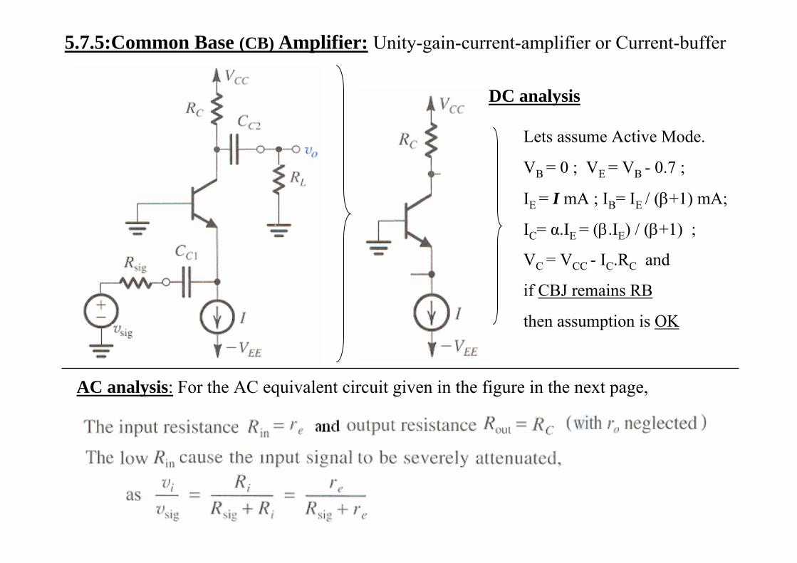
5.7.5:Common Base (CB) Amplifier: Unity-gain-current-amplifier or Current-buffer
DC analysis
Lets assume Active Mode.
VB = 0 ; VE = VB - 0.7 ;
IE = I mA ; IB= IE / (β+1) mA;
IC= α.IE = (β.IE) / (β+1) ;
VC = VCC - IC.RC and
if CBJ remains RB
then assumption is OK
AC analysis: For the AC equivalent circuit given in the figure in the next page,

5.7.5:Common Base (CB) Amplifier: Low Zin makes it not good voltage amplifier
AC analysis
Figures from text book
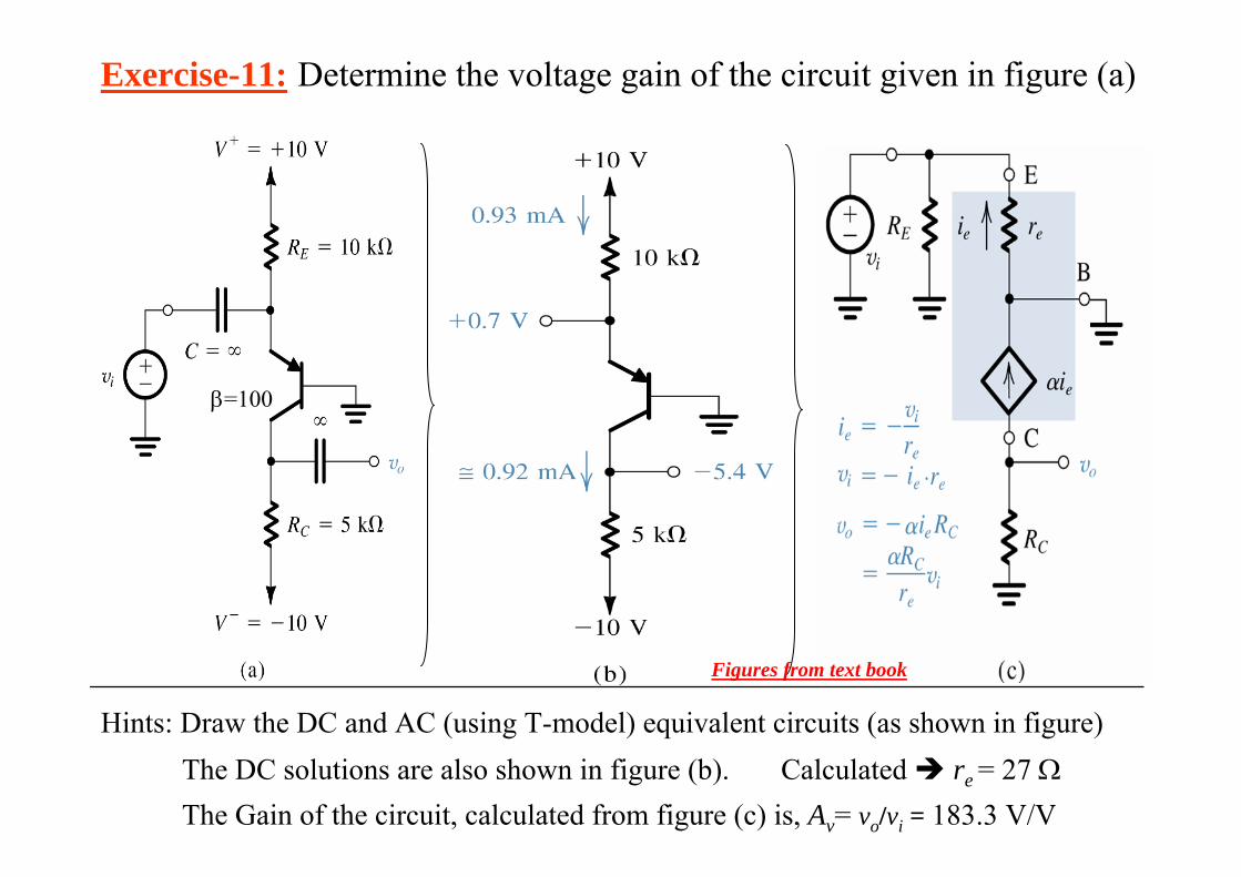
Hints: Draw the DC and AC (using T-model) equivalent circuits (as shown in figure) The DC solutions are also shown in figure (b). Calculated re = 27 ΩThe Gain of the circuit, calculated from figure (c) is, Av= vo/vi = 183.3 V/V
Exercise-11: Determine the voltage gain of the circuit given in figure (a)
β=100
Figures from text book

5.7.5:Common Collector (CC) Amplifier: Emitter FollowerDC analysis Assume Active Mode.
IE=I mA; IB=IE/(β+1)mA
VB =0–(IB)(RB) ;
VE=VB - 0.7 ;
IC=α.IE = (β.IE)/(β+1) ;
VC = VCC
if CBJ remains RB
then assumption is OK
AC analysis Figures from text book

AC analysis
Base to Emitter
Emitter to Base:Figures from text book

Exercises-12
DC use KVL VCC, RB, VBE, RE
Exercises-13the overall voltage gain, Gv
Gv
Gv
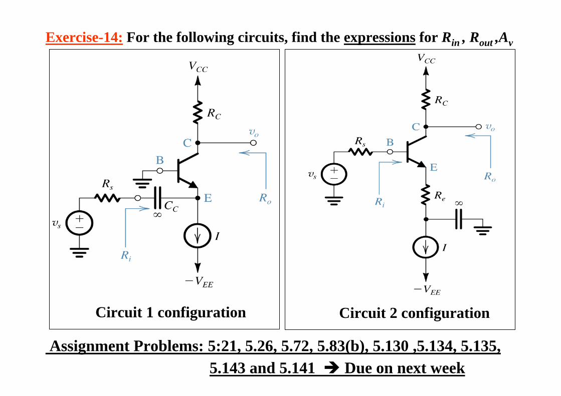
Circuit 1 configuration Circuit 2 configuration
Exercise-14: For the following circuits, find the expressions for Rin , Rout ,Av
Assignment Problems: 5:21, 5.26, 5.72, 5.83(b), 5.130 ,5.134, 5.135, 5.143 and 5.141 Due on next week

Design Criteria of a BJT Amplifier (review):
Figures from text book

Simulation Examples using the Spice software: