graduate institute of electronics engineering, ntu
TRANSCRIPT

ACCESS IC LAB
Graduate Institute of Electronics Engineering, NTU
Memory HierarchyMemory Hierarchy
Lecturer: Chihhao ChaoAdvisor: Prof. An-Yeu Wu
Date: 2009.4.29 Wednesday
Adapted from Prof. Wu’s 計算機結構 Lecture Note

ACCESS IC LAB Graduate Institute of Electronics Engineering, NTU
P2
OutlineOutlinev Review of memory basicsvMemory hierarchyv Cache overviewvMeasuring and improving cache performance

ACCESS IC LAB
Graduate Institute of Electronics Engineering, NTU
Review of Memory BasicsReview of Memory Basics

ACCESS IC LAB Graduate Institute of Electronics Engineering, NTU
P4
Memory Classification & MetricsMemory Classification & Metrics
v Key Design Metrics1. Memory Density (number of bits/um2) and Size2. Access Time (time to read or write) and Throughput3. Power Dissipation
Read-Write MemoryNon-Volatile Read-Write
Memory
Read-Only Memory
Random Access
Non-Random Access EPROM
EEPROMFLASH
Mask-ProgrammedSRAM
DRAMFIFOLIFO

ACCESS IC LAB Graduate Institute of Electronics Engineering, NTU
P5
Memory Array ArchitectureMemory Array Architecture

ACCESS IC LAB Graduate Institute of Electronics Engineering, NTU
P6
Latch and Register Based MemoryLatch and Register Based Memory
vWorks fine for small memory blocksv Simple memory model, simple timing
v Inefficient in area for large memoriesv Density is the key metric in large memory circuits
Positive Latch Negative Latch Register-based Memory

ACCESS IC LAB Graduate Institute of Electronics Engineering, NTU
P7
Static RAM (SRAM) Cell (6Static RAM (SRAM) Cell (6--T Cell)T Cell)
v Logic state held by cross-coupled inverters (M1,M2;M3,M4)v Retain state as long as power supply turns onv Feedback must be overdriven to write into the memory

ACCESS IC LAB Graduate Institute of Electronics Engineering, NTU
P8
Dynamic RAM (DRAM) CellDynamic RAM (DRAM) Cell
v DRAM relies on charge stored in a capacitor to hold logic statev Use in all high density memories (one bit / transistor)v Must be “refreshed” or state will be lost – high overhead
Write: set Bit Line (BL) to 0 or VDD & enable Word Line (WL)Read: set Bit Line (BL) to 0 or VDD/2 & enable Word Line (WL)

ACCESS IC LAB Graduate Institute of Electronics Engineering, NTU
P9
Interacting with a Memory DeviceInteracting with a Memory Device
v Address pins drive row and column decoders
v Data pins are bidirectional and shared by reads and writes
v Output Enable gates the chip’s tristate driver
v Write Enable sets the memory’s read/write mode
v Chip Enable/Chip Select acts as a master switch

ACCESS IC LAB Graduate Institute of Electronics Engineering, NTU
P10
Asynchronous SRAMAsynchronous SRAMv Basic Memory, e.g..
v MCM6264C 8k x 8 SRAMv Bidirectional data bus for
read/writev Chip Enables (E1 and E2)
v E1=1’b0, E2=1’b1 to enable the chip
v Write Enable (W)v active-low when chip is
enabledv Output Enable (G)
v active-low when chip is enabled
On the outside
On the inside

ACCESS IC LAB Graduate Institute of Electronics Engineering, NTU
P11
Asynchronous SRAM Read OperationAsynchronous SRAM Read Operation
v Read cycle begins when all enable signals are active (E1,E2,G)v Data is valid after read access timev Data bus is tristated shortly after G or E1 goes high (inactive)

ACCESS IC LAB Graduate Institute of Electronics Engineering, NTU
P12
Address Controlled ReadsAddress Controlled Reads
v Perform multiple reads without disable chip (G=1’b0)v Data bus after Address bus, after some delayv Note the Bus enable time, Access time, Contamination time, Bus tristate
time

ACCESS IC LAB Graduate Institute of Electronics Engineering, NTU
P13
Asynchronous SRAM Write OperationAsynchronous SRAM Write Operation
v Data latched when W or E1 goes highv Data must be stable at this timev Address must be stable before W goes low (inactive)
v Write waveforms are very importantv Glitches to address can cause write to unexpected address

ACCESS IC LAB Graduate Institute of Electronics Engineering, NTU
P14
Synchronous SRAMSynchronous SRAMv Use synchronization registers to provide synchronous inputs and
encourage more reliable operation at high speed

ACCESS IC LAB Graduate Institute of Electronics Engineering, NTU
P15
Asynchronous DRAM OperationAsynchronous DRAM Operation
v Usually address are separated to Row address and Column addressv Manipulation of RAS and CAS can provide early-write, read-write, hidden-
refresh, ... etc efficient operating modes.

ACCESS IC LAB Graduate Institute of Electronics Engineering, NTU
P16
Key Messages on Memory DevicesKey Messages on Memory Devicesv DRAM vs. SRAM
v SRAM holds states as long as power supply is turned on; DRAM must be refreshed à result in complicated control
v DRAM has much higher density, but requires special capacitor technology
v Handle memory operationsv Primary inputs of memory should be registered for synchronization and
reducing glitchesv It’s bad idea to enable two tri-states driving the bus at the same timev An SRAM doesn’t need to be refreshed while a DRAM doesv A synchronous memory can result in higher throughput

ACCESS IC LAB
Graduate Institute of Electronics Engineering, NTU
Memory HierarchyMemory Hierarchy

ACCESS IC LAB Graduate Institute of Electronics Engineering, NTU
P18
Where are we now?Where are we now?
ACCESS IC LAB Graduate Institute of Electronics Engineering, NTU
P19
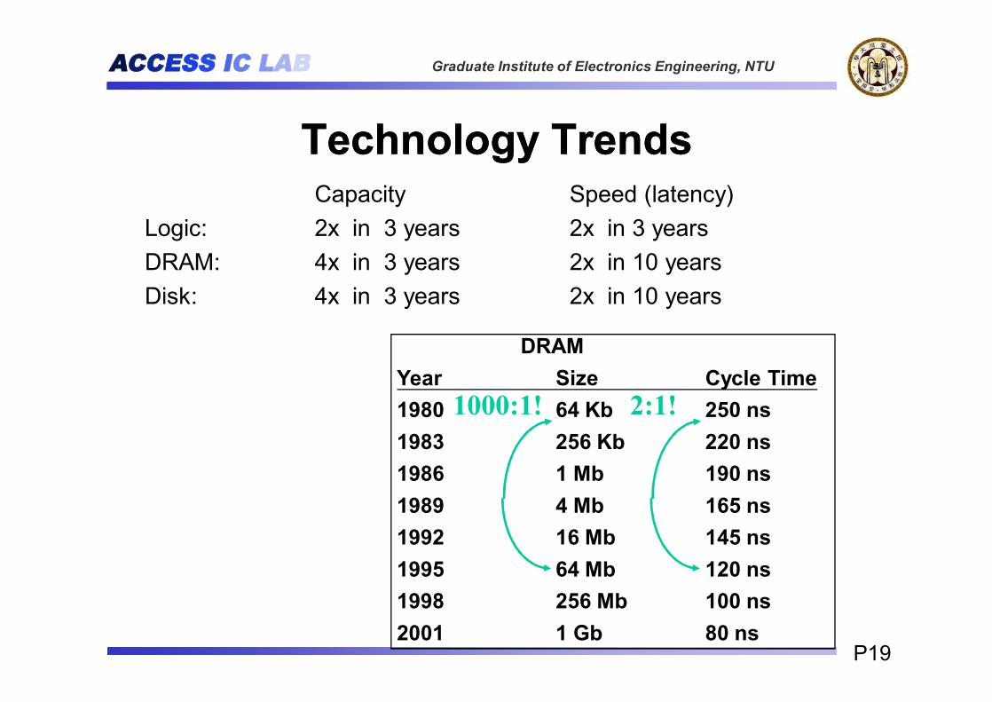
Capacity Speed (latency)Logic: 2x in 3 years 2x in 3 yearsDRAM: 4x in 3 years 2x in 10 yearsDisk: 4x in 3 years 2x in 10 years
DRAMYear Size Cycle Time1980 64 Kb 250 ns1983 256 Kb 220 ns1986 1 Mb 190 ns1989 4 Mb 165 ns1992 16 Mb 145 ns1995 64 Mb 120 ns1998 256 Mb 100 ns2001 1 Gb 80 ns
1000:1! 2:1!
Technology TrendsTechnology Trends
ACCESS IC LAB Graduate Institute of Electronics Engineering, NTU
P20
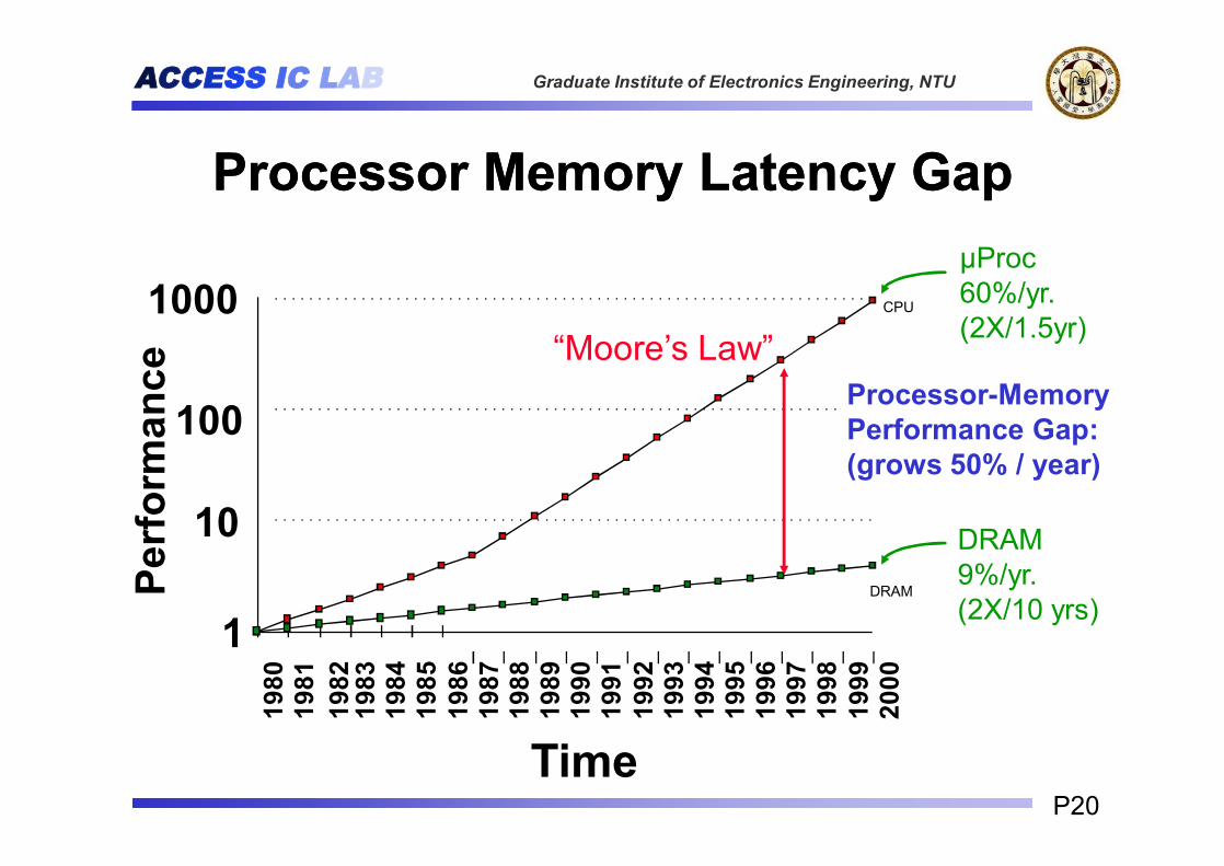
µProc60%/yr.(2X/1.5yr)
DRAM9%/yr.(2X/10 yrs)1
10
100
100019
8019
81
1983
1984
1985
1986
1987
1988
1989
1990
1991
1992
1993
1994
1995
1996
1997
1998
1999
2000
DRAM
CPU
1982
Processor-MemoryPerformance Gap:(grows 50% / year)
Perf
orm
ance
Time
“Moore’s Law”
Processor Memory Latency GapProcessor Memory Latency Gap

ACCESS IC LAB Graduate Institute of Electronics Engineering, NTU
P21
What the Gap means?What the Gap means?vWe use the pipelined MIPS as an example:
Clock period will be bounded by Memory, not Logic!!

ACCESS IC LAB Graduate Institute of Electronics Engineering, NTU
P22
Deep Pipeline in Modern Desktop uPDeep Pipeline in Modern Desktop uP

ACCESS IC LAB Graduate Institute of Electronics Engineering, NTU
P23
Memory Access PatternMemory Access Pattern
vModel the memory access address and access timev Not fully random, e.g. uniform distributedv Usually have some pattern à Here comes the chance!

ACCESS IC LAB Graduate Institute of Electronics Engineering, NTU
P24
v A memory hierarchy consists of multiple levels of memory with different speeds and sizesv Guideline: Build memory as a hierarchy of levels, with the fastest
memory close to the processor, and the slower, less expensive memory below that
v Goal: To present the user with as much as is available in the cheapest technology, while providing access at the speed offered by the fastest memory.
v Three major technologies used to construct memory hierarchy:
Memory hierarchy Typical access time $ per GB in 2004
SRAM 0.5 – 5 ns $4000 - $10000
DRAM 50 – 70 ns $100 - $200
Magnetic disk 5,000,000- 20,000,000 ns $0.5 - $2
Memory HierarchyMemory Hierarchy

ACCESS IC LAB Graduate Institute of Electronics Engineering, NTU
P25
General Principles of MemoryGeneral Principles of Memoryv Definitionsv Upper: memory closer to processorv Block: minimum unit that is present or not presentv Block address: location of block in memory
v Locality + smaller HW is faster = memory hierarchyv Levels: each smaller, faster, more expensive/byte than level
belowv Inclusive: data found in upper leve also found in the lower level
ACCESS IC LAB Graduate Institute of Electronics Engineering, NTU
P26
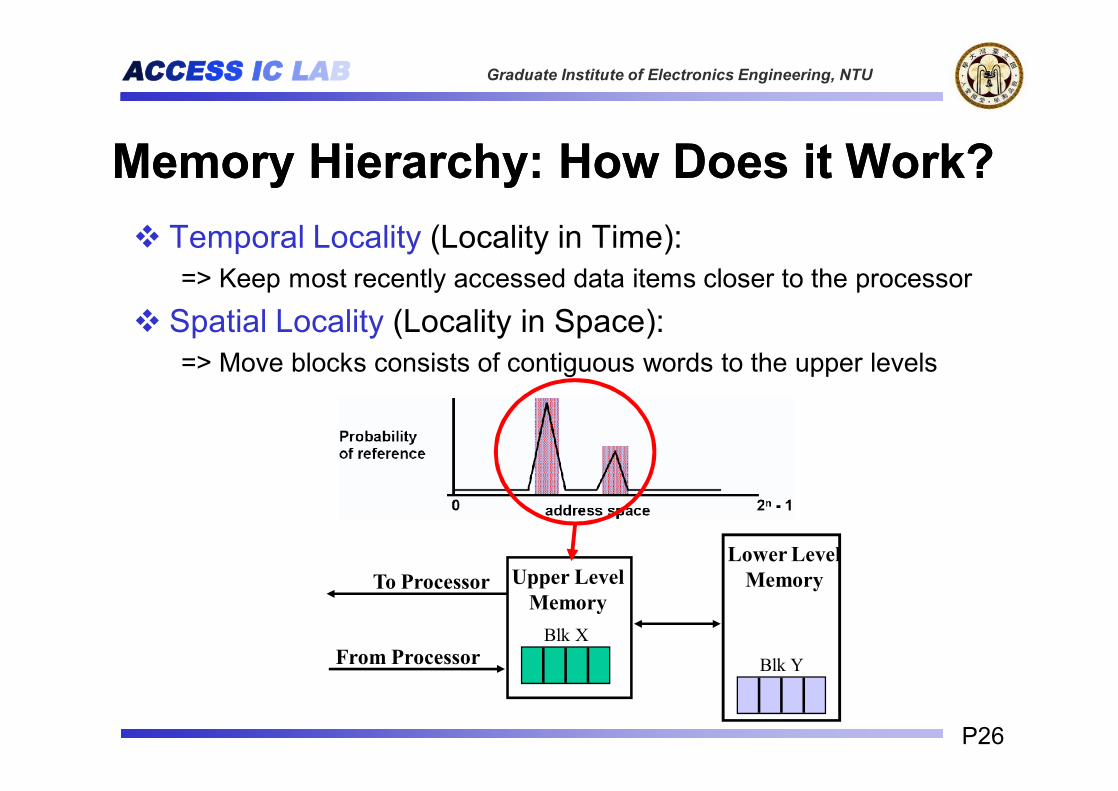
Memory Hierarchy: How Does it Work?Memory Hierarchy: How Does it Work?v Temporal Locality (Locality in Time):
=> Keep most recently accessed data items closer to the processor
v Spatial Locality (Locality in Space):=> Move blocks consists of contiguous words to the upper levels
Lower LevelMemoryUpper Level
MemoryTo Processor
From ProcessorBlk X
Blk Y

ACCESS IC LAB Graduate Institute of Electronics Engineering, NTU
P27
Memory Hierarchy: TerminologyMemory Hierarchy: Terminologyv Hit: data appears in some block in the upper level (example: Block X)
v Hit Rate: the fraction of memory access found in the upper levelv Hit Time: Time to access the upper level which consists of
RAM access time + Time to determine hit/miss
v Miss: data needs to be retrieve from a block in the lower level (Block Y)v Miss Rate = 1 - (Hit Rate)v Miss Penalty: Time to replace a block in the upper level +
Time to deliver the block the processor
v Hit Time << Miss Penalty
Lower LevelMemoryUpper Level
MemoryTo Processor
From ProcessorBlk X
Blk Y

ACCESS IC LAB Graduate Institute of Electronics Engineering, NTU
P28
Memory Hierarchy of a Memory Hierarchy of a Modern Computer SystemModern Computer System
Control
Datapath
SecondaryStorage(Disk)
Processor
Registers
MainMemory(DRAM)
SecondLevelCache
(SRAM)
On-C
hipC
ache
1s 10,000,000s (10s ms)
Speed (ns): 10s 100s
100s GsSize (bytes): Ks Ms
TertiaryStorage(Tape)
10,000,000,000s (10s sec)
Ts

ACCESS IC LAB Graduate Institute of Electronics Engineering, NTU
P29
A Typical Memory Hierarchy of Modern A Typical Memory Hierarchy of Modern Computer SystemComputer System

ACCESS IC LAB
Graduate Institute of Electronics Engineering, NTU
Cache OverviewCache Overview

ACCESS IC LAB Graduate Institute of Electronics Engineering, NTU
P31
Inside a CacheInside a Cache

ACCESS IC LAB Graduate Institute of Electronics Engineering, NTU
P32
The Basics of CacheThe Basics of Cache

ACCESS IC LAB Graduate Institute of Electronics Engineering, NTU
P33
v Cache: a safe place for hiding or storing things.v Example: Before the request, the cache contains a collection of recent
references X1, X2, ………., Xn-1, and the processor requests a word Xnthat is not in the cache. This request results in a miss, and the word Xn is brought form memory into cache. à Replacement Policy
The Basics of The Basics of Cache (2)Cache (2)
X4
X1
Xn-2
Xn-1
X2
X3
X4
X1
Xn-2
Xn-1
X2
Xn
X3
Before the reference to Xn After the reference to Xn

ACCESS IC LAB Graduate Institute of Electronics Engineering, NTU
P34
Four Questions for Memory Four Questions for Memory Hierarchy DesignersHierarchy Designers
v Q1: Where can a block be placed in the upper level? (Block placement)
v Q2: How is a block found if it is in the upper level?(Block identification)
v Q3: Which block should be replaced on a miss? (Block replacement)
v Q4: What happens on a write? (Write strategy)

ACCESS IC LAB Graduate Institute of Electronics Engineering, NTU
P35
Q1: Where can a block be placed?Q1: Where can a block be placed?v Direct Mapped: Each block has only one place that it
can appear in the cache.
v Fully associative: Each block can be placed anywhere in the cache.
v Set associative: Each block can be placed in a restricted set of places in the cache.v If there are n blocks in a set, the cache placement is called
n-way set associative
vWhat is the associativity of a direct mapped cache?

ACCESS IC LAB Graduate Institute of Electronics Engineering, NTU
P36
Placement Placement PolicyPolicy

ACCESS IC LAB Graduate Institute of Electronics Engineering, NTU
P37
Associative structuresAssociative structures

ACCESS IC LAB Graduate Institute of Electronics Engineering, NTU
P38
Q2: How Is a Block Found?Q2: How Is a Block Found?
v The address can be divided into two main partsv Block offset: selects the data from the block
offset size = log2(block size)v Block address: tag + index
Ø index: selects set in cacheindex size = log2(#blocks/associativity)
Ø tag: compared to tag in cache to determine hittag size = addreess size - index size - offset size
v Each block has a valid bit that tells if the block is valid - the block is in the cache if the tags match and the valid bit is set.

ACCESS IC LAB Graduate Institute of Electronics Engineering, NTU
P39
Valid Bit of CacheValid Bit of Cache
v Add a “valid bit” to indicate whether an entry contains a valid address.
v Replacement policy: recently accessed words replace less-recently referenced words. (use temporal locality)

ACCESS IC LAB Graduate Institute of Electronics Engineering, NTU
P40
Direct Mapped Cache ArchitectureDirect Mapped Cache Architecture

ACCESS IC LAB Graduate Institute of Electronics Engineering, NTU
P41
22--Way SetWay Set--Associative Cache ArchitectureAssociative Cache Architecture

ACCESS IC LAB Graduate Institute of Electronics Engineering, NTU
P42
Fully Associative Cache ArchitectureFully Associative Cache Architecture

ACCESS IC LAB Graduate Institute of Electronics Engineering, NTU
P43
Q3: Which Block Should be Replaced Q3: Which Block Should be Replaced on a Miss?on a Miss?
vEasy for Direct Mapped - only one candidatevSet Associative or Fully Associative:vRandom - easier to implement
vLeast Recently Used (LRU) - harder to implement
Ø true implementation only feasible for small sets (2-way)
Ø cache state must be updated on every access
v First-In, First-Out (FIFO) or Round-RobinØ usually used in highly associative sets
v Not Least Recently UsedØ FIFO with exception for most recently used blocks

ACCESS IC LAB Graduate Institute of Electronics Engineering, NTU
P44
ExampleExamplevMiss rates for caches with different size, associativity
and replacement algorithm.
Associativity: 2-way 4-way 8-waySize LRU Random LRU Random LRU Random16 KB 5.18% 5.69% 4.67% 5.29% 4.39% 4.96%64 KB 1.88% 2.01% 1.54% 1.66% 1.39% 1.53%256 KB 1.15% 1.17% 1.13% 1.13% 1.12% 1.12%
For caches with low miss rates, random is almost as good as LRU.
ACCESS IC LAB Graduate Institute of Electronics Engineering, NTU
P45
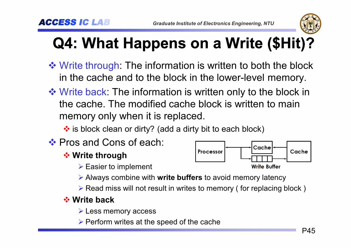
Q4: What Happens on a Q4: What Happens on a Write ($Hit)?Write ($Hit)?vWrite through: The information is written to both the block
in the cache and to the block in the lower-level memory.vWrite back: The information is written only to the block in
the cache. The modified cache block is written to main memory only when it is replaced.v is block clean or dirty? (add a dirty bit to each block)
v Pros and Cons of each:vWrite throughØ Easier to implementØ Always combine with write buffers to avoid memory latencyØRead miss will not result in writes to memory ( for replacing block )
vWrite backØ Less memory accessØ Perform writes at the speed of the cache
ACCESS IC LAB Graduate Institute of Electronics Engineering, NTU
P46
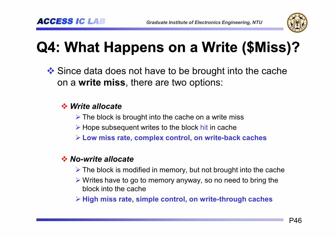
Q4: What Happens on a Q4: What Happens on a Write ($Miss)?Write ($Miss)?v Since data does not have to be brought into the cache
on a write miss, there are two options:
vWrite allocateØ The block is brought into the cache on a write missØHope subsequent writes to the block hit in cacheØ Low miss rate, complex control, on write-back caches
v No-write allocateØ The block is modified in memory, but not brought into the cacheØWrites have to go to memory anyway, so no need to bring the
block into the cacheØHigh miss rate, simple control, on write-through caches

ACCESS IC LAB Graduate Institute of Electronics Engineering, NTU
P47
Calculating Bits in CacheCalculating Bits in Cachev How many total bits are needed for a direct- mapped cache with
64 KBytes of data and 8 word blocks, assuming a 32-bit address?
v 64 Kbytes = 214 words = (214)/8 = 211 blocksv block size = 32 bytes à offset size = 5 bits, v #sets = #blocks = 211à index size = 11 bitsv tag size = address size - index size - offset size = 32 - 11 - 5 = 16 bits v bits/block = data bits + tag bits + valid bit = 8x32 + 16 + 1 = 273 bitsv bits in cache = #blocks x bits/block = 211 x 273 = 68.25 Kbytes
v Increase block size => decrease bits in cache

ACCESS IC LAB Graduate Institute of Electronics Engineering, NTU
P48
Calculating Bits in CacheCalculating Bits in Cachev How many total bits are needed for a direct- mapped cache with 64
KBytes of data and one word blocks, assuming a 32-bit address?v 64 Kbytes = 16 K words = 214 words = 214 blocksv block size = 4 bytes à offset size = 2 bits, v #sets = #blocks = 214à index size = 14 bitsv tag size = address size - index size - offset size = 32 - 14 - 2 = 16 bits v bits/block = data bits + tag bits + valid bit = 32 + 16 + 1 = 49v bits in cache = #blocks x bits/block = 214 x 49 = 98 Kbytes
v How many total bits would be needed for a 4-way set associative cache to store the same amount of datav block size and #blocks does not changev #sets = #blocks/4 = (214)/4 = 212à index size = 12 bitsv tag size = address size - index size - offset = 32 - 12 - 2 = 18 bitsv bits/block = data bits + tag bits + valid bit = 32 + 18 + 1 = 51v bits in cache = #blocks x bits/block = 214 x 51 = 102 Kbytes
v Increase associativityà Increase bits in cache

ACCESS IC LAB
Graduate Institute of Electronics Engineering, NTU
Measuring and Improving Measuring and Improving Cache PerformanceCache Performance

ACCESS IC LAB Graduate Institute of Electronics Engineering, NTU
P50
Measuring Cache PerformanceMeasuring Cache PerformanceCPU time = (CPU execution clock cycles + Memory-stall clock cycles)
* Clock cycle time
Memory-stall clock cycles come primarily from cache misses:Memory-stall clock cycles = Read-stall cycles + Write-stall cyclesRead-stall cycles = (reads/program) * read miss rate * read miss penaltyWrite-stall cycles = ((writes/ program) * write miss rate * write miss penalty) +
write buffer stalls
v For a write-back scheme: v It has potential additional stalls arising from the need to write a cache block to memory
when the block is replaced.v For a write-through scheme:
v Write miss requires that we fetch the block before continuing the write.v Write buffer stalls: The write buffer is full when a write occurs.

ACCESS IC LAB Graduate Institute of Electronics Engineering, NTU
P51
v In most write-through scheme, we assume:v Read and write miss penalty are the same.v Write buffer stall is negligible.
(1) Memory-stall clock cycles = (Memory accesses/Program) * Miss rate * Miss penalty
(2) Memory-stall clock cycles = (Instructions/Program) * (Misses/Instruction) * Miss penalty
Measuring Cache PerformanceMeasuring Cache Performance

ACCESS IC LAB Graduate Institute of Electronics Engineering, NTU
P52
v (question) How much faster a processor would run with perfect cache that never missed?
v (answer) Assumptions:v An instruction cache miss = 2%v A data cache miss rate = 4%v CPI = 2 without any memory stallsvMiss penalty = 100 cycles for all missesv Use the instruction frequencies for SPECint2000 from Chapter3,
Fig3.26 on page 228.v Instruction count = I
Calculating cache performanceCalculating cache performance

ACCESS IC LAB Graduate Institute of Electronics Engineering, NTU
P53
Instruction miss cycles = I * 2% * 100 = 2.00 IData miss cycles = I * 36% * 4% * 100 = 1.44 ITotal number of memory-stall cycles = 2.00 I + 1.44 I = 3.44 IThe CPI with memory stalls is 2 + 3.44 = 5.44Since there is no change in instruction count or clock rate, the ratio of the CPU execution times =
CPU time with stalls I * CPIstall clock cycleCPU time with perfect cache I * CPIperfect clock cycle
CPIstall 5.44CPIperfect 2
Calculating cache performanceCalculating cache performance
2.72

ACCESS IC LAB Graduate Institute of Electronics Engineering, NTU
P54
v Example: Suppose we speed up the computer in the previous example by reducing CPI from 2 to 1.
v The system with cache misses has a CPI of 1 + 3.44 = 4.44.v The system with the perfect cache = 4.44 / 1 = 4.44 times faster.v The amount of execution time spent on memory stalls rises from
3.44 / 5.44 = 63% to 3.44 / 4.44 = 77%
Calculating cache performanceCalculating cache performance

ACCESS IC LAB Graduate Institute of Electronics Engineering, NTU
P55
v Example: cache performance with increased clock rate(question)
How much faster will the computer be with the faster clock, assuming the same miss rate ad the previous example? (answer) v The new miss penalty = 200 clock cyclesv Total miss cycles per instruction = (2%*200)+36%*(4%*200) = 6.88v CPI = 2 + 6.88 = 8.88
Calculating cache performanceCalculating cache performance
The relative performance =performance with fast clock
performance with slow clockIC * CPIslow * clock cycle
IC * CPIfast * (clock cycle/2)
5.44
8.88/21.23
The computer with faster clock is about 1.2 times faster rather than 2times faster, which it have been if we ignored cache misses.

ACCESS IC LAB Graduate Institute of Electronics Engineering, NTU
P56
v Reducing cache misses by more flexible placement of blocksv (1) Direct mapped cache:
A block can go in exactly one place in the cache.v (2) Fully-associative cache:
A cache structure in which a block can be placed in any location in the cache.
v (3) Set-associative cache:A cache that has a fixed number of locations (at least two) where each block can be placed.
v In direct-mapped cache, the position of a memory block is given by (block number) modulo (number of cache blocks)
v In a set-associative cache, the set containing a memory block is given by (block number) modulo (number of set in the cache).
Calculating cache performanceCalculating cache performance

ACCESS IC LAB Graduate Institute of Electronics Engineering, NTU
P57
BlockBlock--Size TradeSize Trade--OffOff
Increase block size tends to decrease miss rate
miss rate
block size (bytes)

ACCESS IC LAB Graduate Institute of Electronics Engineering, NTU
P58
BlockBlock--Size TradeSize Trade--OffOffv Larger block size à spatial locality (good) à reduce
miss ratiov Larger miss penaltyv Block is too largeàless blocks in cacheàmiss rate goes up
v Avg access time = hit time * (1- miss rate) + miss penalty * miss rate

ACCESS IC LAB Graduate Institute of Electronics Engineering, NTU
P59
Increase Memory Bandwidth to Reduce Increase Memory Bandwidth to Reduce Miss PenaltyMiss Penalty
ACCESS IC LAB Graduate Institute of Electronics Engineering, NTU
P60
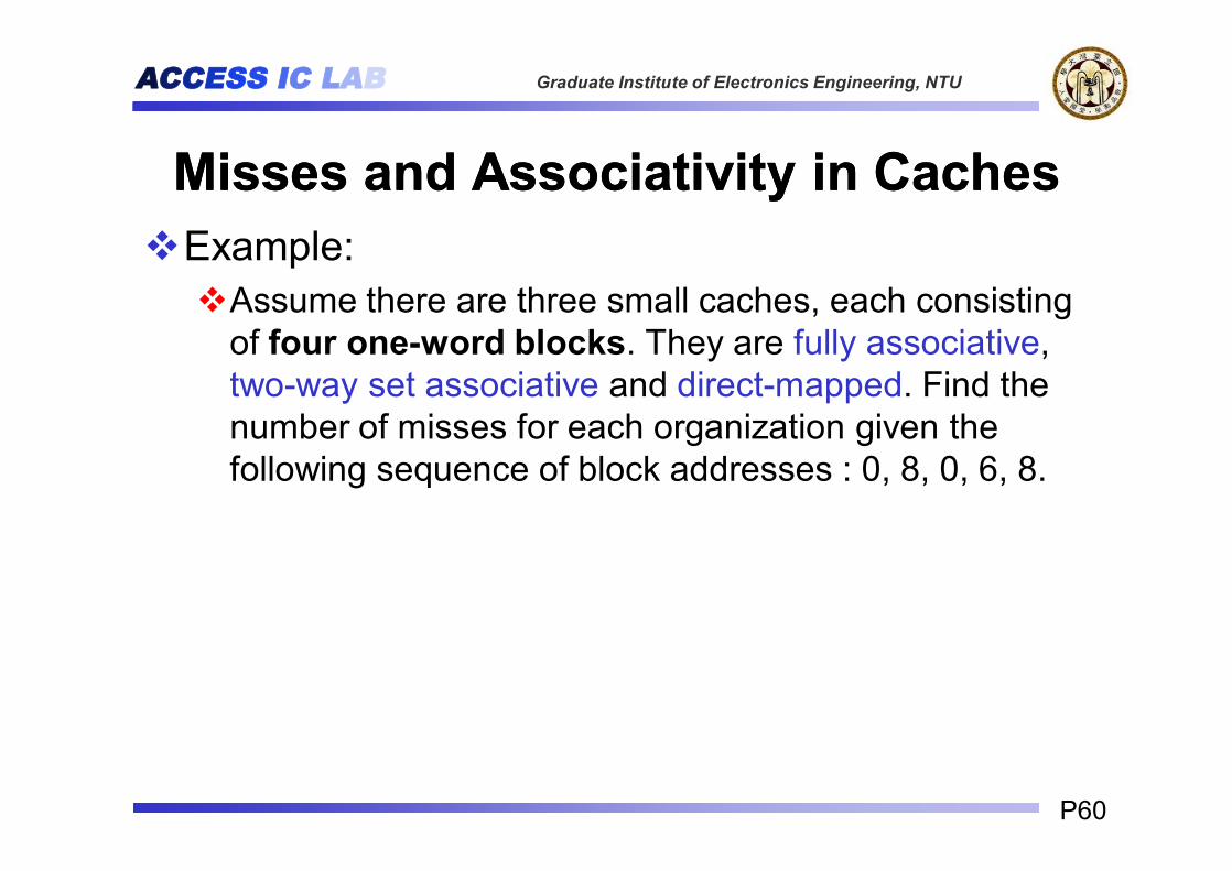
Misses and Associativity in CachesMisses and Associativity in CachesvExample: vAssume there are three small caches, each consisting
of four one-word blocks. They are fully associative, two-way set associative and direct-mapped. Find the number of misses for each organization given the following sequence of block addresses : 0, 8, 0, 6, 8.

ACCESS IC LAB Graduate Institute of Electronics Engineering, NTU
P61
Misses in DirectMisses in Direct--mapped Cachemapped Cache
The direct-mapped cache generates 5 misses for the five accesses.
Address of memory
block accessed
Hit or
miss
Contents of cache blocksafter reference
0 1 2 3
0 miss Memory[0]
8 miss Memory[8]
0 miss Memory[0]
6 miss Memory[0] Memory[6]
8 miss Memory[8] Memory[6]
nSequence of block addresses : 0, 8, 0, 6, 8.
Block address Cache block
0 (0 modulo 4) = 0
6 (6 modulo 4) = 2
8 (8 modulo 4) = 0

ACCESS IC LAB Graduate Institute of Electronics Engineering, NTU
P62
Misses in 2Misses in 2--Way SetWay Set--Associative CacheAssociative Cache
The two-way set associative cache has 4 misses.
Address of memory
block accessed
Hit or
miss
Contents of cache blocksafter reference
0 0 1 1
0 miss Memory[0]8 miss Memory[0] Memory[8]0 hit Memory[0] Memory[8]6 miss Memory[0] Memory[6]8 miss Memory[8] Memory[6]
Block address Cache block
0 (0 modulo 2) = 0
6 (6 modulo 2) = 0
8 (8 modulo 2) = 0

ACCESS IC LAB Graduate Institute of Electronics Engineering, NTU
P63
Misses in Fully Associative CacheMisses in Fully Associative Cache
The fully associative cache only has 3 misses: the best one
Address of memory
block accessed
Hit or
miss
Contents of cache blocksafter reference
0 0 0 0
0 miss Memory[0]
8 miss Memory[0] Memory[8]
0 hit Memory[0] Memory[8]
6 miss Memory[0] Memory[8] Memory[6]
8 hit Memory[0] Memory[8] Memory[6]

ACCESS IC LAB Graduate Institute of Electronics Engineering, NTU
P64
FourFour--way setway set--associative cacheassociative cache

ACCESS IC LAB Graduate Institute of Electronics Engineering, NTU
P65
Size of tags v.s. Set associativitySize of tags v.s. Set associativityv Question: v Assume a cache of 4K caches, a four-word block size, and a 32-bit
address. Find the total number of sets and the total number tag bits for caches that are direct-mapped, two-way and four-way set associative and fully associative.
v Answer:v direct-mapped: Ø The bits for index and tag = 32 – 4 = 28 (4=block offset)Ø The number of sets = the number of blocks = 4KØ The bits for index = log2(4K) = 12Ø The total number of tag bits = (28 - 12) * 4K = 64K bits

ACCESS IC LAB Graduate Institute of Electronics Engineering, NTU
P66
Size of tags v.s. Set associativitySize of tags v.s. Set associativityv Two-way set associative:Ø The number of sets = (the number of blocks) / 2 = 2KØ The total number of tag bits = (28 - 11) * 2 * 2K = 68K bits
v Four-way set associative:Ø The number of sets = (the number of blocks) / 4 = 1KØ The total number of tag bits = (28 - 10) * 4 * 1K = 72K bits
v Fully set associative:Ø The number of sets = 1Ø The total number of tag bits = 28 * 4K * 1= 112K bits
v Least recently used (LRU): A replacement scheme in which the block replaced is the one that has been unused for the longest time.

ACCESS IC LAB Graduate Institute of Electronics Engineering, NTU
P67
Multilevel cacheMultilevel cachevMultilevel cache: A memory hierarchy with multiple levels of
caches, rather than just a cache and main memory.
v Example: v Suppose we have a processor with a base CPI of 1.0, assuming all
reference hit in the primary cache, and a clock rate of 5GHz. v Assume a main memory access time of 100 ns, including all the miss
handling. Suppose the miss rate per instruction at the primary cache is 2%.
v How much faster will the processor be if we add a secondary cachethat has a 5 ns access time for either a hit or a miss, and is large enough to reduce the miss rate to the main memory to 0.5%?

ACCESS IC LAB Graduate Institute of Electronics Engineering, NTU
P68
Multilevel cache (contMultilevel cache (cont’’d)d)v For the processor with one level of cache:
The miss penalty to main memory = 100ns/ 0.2ns (1/5GHz) = 500 clock cycles.Total CPI = base CPI + memory-stall cycles per instruction.Total CPI = 1.0 + 2% * 500 = 11.0
v For the processor with two levels of cache:The miss penalty for an access to second-level cache = 5 / 0.2 = 25 clock cycles.Total CPI = base CPI + primary stalls per instruction + secondary stalls per instruction .Total CPI = 1.0 + 2% * 25 + 0.5% * 500 = 4.0
v The processor with the secondary cache is faster by 11.0 / 4.0 = 2.8

ACCESS IC LAB Graduate Institute of Electronics Engineering, NTU
P69
Embed Cache Into Pipelined MIPSEmbed Cache Into Pipelined MIPS