complexity management & improve timing, area,...
TRANSCRIPT

ACCESS IC LAB
Graduate Institute of Electronics Engineering, NTU
Complexity Management &Complexity Management &Improve Timing, Area, and PowerImprove Timing, Area, and Power
Lecturer: Chih-Hao Chao (趙之昊)Date: 2009.4.8

Graduate Institute of Electronics Engineering, NTU
OutlineOutlinevManaging Complexity for Large DesignvSteps in High-Level DesignvDesign Partitioning
vImprove Timing, Area, and PowervPerformance metricsvPipeliningvParallelizingvRetimingvLow power design techniques
pp. 2Complexity Management & Improve Timing, Area, & Power 2009.4.8 Chihhao Chao

Graduate Institute of Electronics Engineering, NTU
Complexity Management for Large DesignsComplexity Management for Large Designsv Given a design spec., novice designers are often
tempted to start coding straightly.v Result it poor quality design
v Time-spending paper works before coding is more than rewarded with a smaller, faster design, and a much quicker debugging cycle.
v Here we present a structured approach to generate a “paper design”.
pp. 3Chihhao ChaoComplexity Management & Improve Timing, Area, & Power 2009.4.8

Graduate Institute of Electronics Engineering, NTU
Basic Guiding PrinciplesBasic Guiding PrinciplesvClearly separate datapath from controllervDatapath: arithmetic/logic units, data registers,
data mux, bus…vDatapath is the hardware units to compute the
desired output results.vController: FSM, counter…vController is the hardware who orchestrate
datapath to deliver correct operations on data.
pp. 4Chihhao ChaoComplexity Management & Improve Timing, Area, & Power 2009.4.8

Graduate Institute of Electronics Engineering, NTU
Steps in HighSteps in High--Level DesignLevel Design1. Structuring the Datapath2. Identify Control Points3. Determine Transition Points in Control Flow4. Determine Control Strategy and Control
Flow5. Determine the Reset Strategy6. Verify before Coding
pp. 5Chihhao ChaoComplexity Management & Improve Timing, Area, & Power 2009.4.8
Graduate Institute of Electronics Engineering, NTU
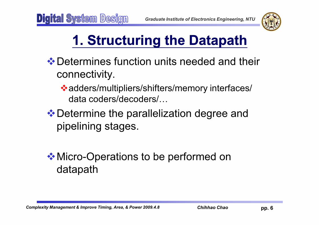
1. Structuring the Datapath1. Structuring the DatapathvDetermines function units needed and their
connectivity.vadders/multipliers/shifters/memory interfaces/
data coders/decoders/…vDetermine the parallelization degree and
pipelining stages.
vMicro-Operations to be performed on datapath
pp. 6Chihhao ChaoComplexity Management & Improve Timing, Area, & Power 2009.4.8

Graduate Institute of Electronics Engineering, NTU
2. Identify Control Points2. Identify Control Points
vControl points consist of control lines and status lines.vControl lines originate in the controller and
determine the detailed operations to be proformedon the datapath.vStatus lines originate in the datapath and indicate
the status output of important units, e.g. flags such as overflow.
pp. 7Chihhao ChaoComplexity Management & Improve Timing, Area, & Power 2009.4.8

Graduate Institute of Electronics Engineering, NTU
3. Determine Transition Points and 3. Determine Transition Points and Control FlowControl Flow
vIdentify control points in the control sequence.ve.g. When to activate Start, Stop signals, vDefine the relationship between key control signal
and state logic of FSM
pp. 8Chihhao ChaoComplexity Management & Improve Timing, Area, & Power 2009.4.8
Graduate Institute of Electronics Engineering, NTU
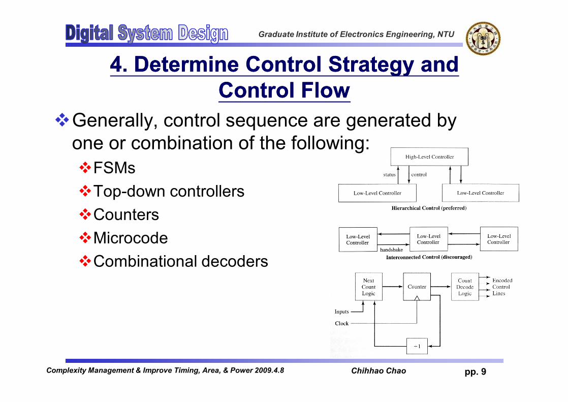
4. Determine Control Strategy and 4. Determine Control Strategy and Control FlowControl Flow
vGenerally, control sequence are generated by one or combination of the following:vFSMsvTop-down controllersvCountersvMicrocodevCombinational decoders
pp. 9Chihhao ChaoComplexity Management & Improve Timing, Area, & Power 2009.4.8

Graduate Institute of Electronics Engineering, NTU
MicroCodeMicroCode & Combinational Decoder& Combinational Decoder
pp. 10Chihhao ChaoComplexity Management & Improve Timing, Area, & Power 2009.4.8

Graduate Institute of Electronics Engineering, NTU
5. Determine the Reset Strategy5. Determine the Reset StrategyvReset is a global signal distributed across the
entire chip.vInitialize the chip to a known state.
vEspecially be careful on how to reset the controller à determines correctness of control sequence
pp. 11Chihhao ChaoComplexity Management & Improve Timing, Area, & Power 2009.4.8

Graduate Institute of Electronics Engineering, NTU
6. Verify before Coding6. Verify before CodingvGenerally, it is a useful practice to hand-
simulate the design before coding.
vDraw a timing diagram capturing critical events (state transition and signal change) to help you find potential bugs early.
pp. 12Chihhao ChaoComplexity Management & Improve Timing, Area, & Power 2009.4.8

Graduate Institute of Electronics Engineering, NTU
Guidelines for Design PartitioningGuidelines for Design Partitioningv Only modules at the bottom of the hierarchy should contain
datapath logic.v Higher level modules contain control logic and instance of sub-module
which contain datapath.v Better synthesis quality
v Critical path should be contained entirely within one module.vWhenever possible, register the outputs of modules.v Potentially sharable resources should be within one module.v Separate modules that will have different synthesis strategies.
v Keep modules as small as possible consistent with the above guide lines.
pp. 13Chihhao ChaoComplexity Management & Improve Timing, Area, & Power 2009.4.8

Graduate Institute of Electronics Engineering, NTU
OutlineOutlinevManaging Complexity for Large DesignvSteps in High-Level DesignvDesign Partitioning
vImprove Timing, Area, and PowervPerformance metricsvPipeliningvParallelizingvRetimingvLow power design techniques
pp. 14Complexity Management & Improve Timing, Area, & Power 2009.4.8 Chihhao Chao

Graduate Institute of Electronics Engineering, NTU
IntroductionIntroductionvWhen design in RTL, the designer need to be
aware of timing, area and power issues.vMeeting timing requirement is the most
critical goal in design. Only optimize for power or area after timing is met.vSynthesis tools operate in gate level, and
cannot resolve all timing, area and power issues.
pp. 15Complexity Management & Improve Timing, Area, & Power 2009.4.8 Chihhao Chao

Graduate Institute of Electronics Engineering, NTU
Timing issuesTiming issuesv Performance v Latency – How many cycles (or how long) does it
take to deliver a particular operation?v Throughput – How many operations can be
completed per second?v Throughput = clock frequency / cycles per operation
Latency = 3 clock cycles, 30nsThroughput = 100Mbits/second
clock frequency = 100MHz
pp. 16Complexity Management & Improve Timing, Area, & Power 2009.4.8 Chihhao Chao

Graduate Institute of Electronics Engineering, NTU
Timing requirementTiming requirementv To fit system throughput, the timing (clock period)
must be smaller than some value.
v In IC design industry, the design must meet timing with margin, and using worst-case library model.
v If the post-synthesis simulation (under a clock period larger than target one) cannot pass the verification to deliver certain throughput, we need to improve the timing.
pp. 17Complexity Management & Improve Timing, Area, & Power 2009.4.8 Chihhao Chao

Graduate Institute of Electronics Engineering, NTU
How to improve timing in DesignHow to improve timing in DesignvPipelining : Exploits temporal parallelismvInsert pipeline registers without changing the
coherence of the datavShorten critical pathvReduce achievable clock periodvTrade off latency (in cycles) to improve throughput
vParallelizing : vDuplicate function units working in parallelvImprove throughput without shorten critical path
pp. 18Complexity Management & Improve Timing, Area, & Power 2009.4.8 Chihhao Chao

Graduate Institute of Electronics Engineering, NTU
Concept of PipeliningConcept of Pipelining
pp. 19
fpipeline < 2 / Tmax
data_in CombLogic
CombLogic
fclock < 1/Tmax
data_inOutput
RegistersMulti-level Logicdata_out
InputRegisters
InputRegisters
PipelineRegister
OutputRegisters
data_out
Tmax
Tmax/ 2
Original
2-stage pipelining
Complexity Management & Improve Timing, Area, & Power 2009.4.8 Chihhao Chao

Graduate Institute of Electronics Engineering, NTU
Example 1: Simple CircuitExample 1: Simple Circuit
pp. 20Complexity Management & Improve Timing, Area, & Power 2009.4.8 Chihhao Chao

Graduate Institute of Electronics Engineering, NTU
Example 2: Pipelined 16Example 2: Pipelined 16--bit Adderbit Adder
pp. 21
Original
2-stage pipelining
Complexity Management & Improve Timing, Area, & Power 2009.4.8 Chihhao Chao

Graduate Institute of Electronics Engineering, NTU
Example 3: FIRExample 3: FIR
pp. 22
2-stage pipeliningOriginal
w(n) = ax(n) + bx(n-1)y(n) = cx(n-2) + w(n)
w(n-1) = ax(n-1) + bx(n-2)y(n-1) = cx(n-3) + w(n-1)
critical path = TMUL + 2TADD critical path = TMUL + TADD
Complexity Management & Improve Timing, Area, & Power 2009.4.8 Chihhao Chao

Graduate Institute of Electronics Engineering, NTU
Pipeline OverheadPipeline Overhead
v Area: pipeline registers
v Increase cycle latencyv Insert N stage pipeline registers, add N cycle latency
v Increase timing latency: shorter clock period, butv Register has setup time overhead à increase critical path
v Non-ideal separation of critical path à not 1/N period
Ø To approach the ideal separation, we needs to know gate-level timing well for balancing the partition of the critical path.
pp. 23Complexity Management & Improve Timing, Area, & Power 2009.4.8 Chihhao Chao

Graduate Institute of Electronics Engineering, NTU
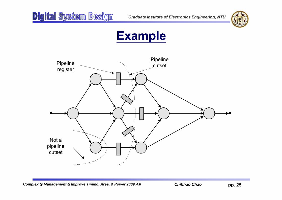
How to do pipelining?How to do pipelining?v Draw the circuit diagram in to a directed graphv Put pipeline registers on feed-forward cut-set of the
graph
v A cutset is a set of edges of a graph such that if the they are removed from the graph, the graph becomes disjoint.
v Feed-forward cut-set: all the removed edges have the same direction from one disjoint set to another. We call it pipeline cut-set.
pp. 24Complexity Management & Improve Timing, Area, & Power 2009.4.8 Chihhao Chao
Graduate Institute of Electronics Engineering, NTU
ExampleExample
Pipelinecutset
Not apipelinecutset
Pipelineregister
pp. 25Complexity Management & Improve Timing, Area, & Power 2009.4.8 Chihhao Chao
Graduate Institute of Electronics Engineering, NTU
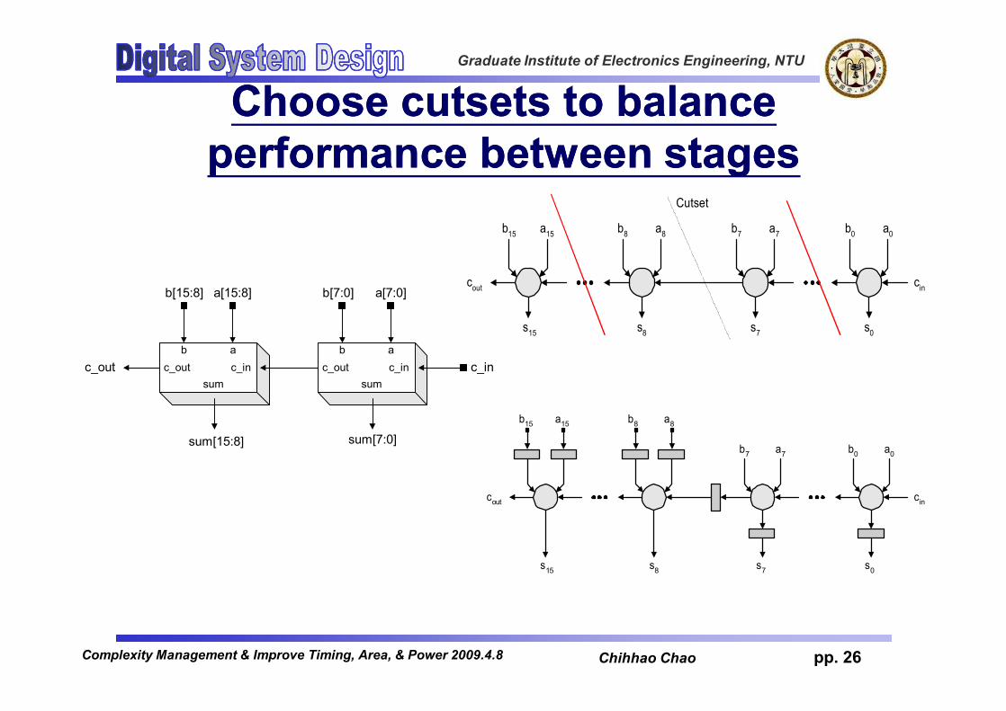
Choose Choose cutsetscutsets to balance to balance performance between stagesperformance between stages
c_outsum
b ac_inc_out
sum
b ac_in
sum[7:0]sum[15:8]
c_out c_in
b[15:8] a[15:8] b[7:0] a[7:0]
b15 a15 b8 a8 b7 a7 b0 a0
cincout
s15 s8 s7 s0
Cutset
b15 a15 b8 a8
b7 a7 b0 a0
cincout
s15 s8 s7 s0
pp. 26Complexity Management & Improve Timing, Area, & Power 2009.4.8 Chihhao Chao

Graduate Institute of Electronics Engineering, NTU
Pipelined 16Pipelined 16--bit Adder Structurebit Adder Structure
c_outsum
b ac_in
PR[15:0]
c_inb[15:0] a[15:0]
c_outsum
b ac_in
sum[7:0]
IR[24:17]
sum[15:0]c_out
clock
b[7:0] a[7:0]b[15:8]
IR[32:25]
IR[16:9] IR[8:1] IR[0]
Input Register: IR[32:0]
Pipeline Register: PR[7:0]
Output Register: OR[16:0]
PR[16:9]PR[24:17]PR[8]
a[15:8]
pp. 27Chihhao Chao

Graduate Institute of Electronics Engineering, NTU
Timing diagram for pipelined adderTiming diagram for pipelined adder
(4)clock
x
aLaR(1)x
bLbR(1)
aLaR(2)
bLbR(2)
aLaR(3)
bLbR(3)
x aLaRbLbR(1) aLaRbLbR(2) aLaRbLbR(3)
(1) (2) (3)
x aLbL(3) sumR(3)aLbL(2) sumR(2)aLbL(1) sumR(1)
x sumL(3) sumR(3)sumL(2) sumR(2)sumL(1) sumR(1)
(5)
IR
PR
OR
a
b
pp. 28Complexity Management & Improve Timing, Area, & Power 2009.4.8 Chihhao Chao

Graduate Institute of Electronics Engineering, NTU
Simulation ResultSimulation Result
pp. 29Complexity Management & Improve Timing, Area, & Power 2009.4.8 Chihhao Chao

Graduate Institute of Electronics Engineering, NTU
module add_16_pipe (c_out, sum, a, b, c_in, clock);parameter size = 16;parameter half = size / 2;parameter double = 2 * size;parameter triple = 3 * half;parameter size1 = half -1; // 7parameter size2 = size -1; // 15parameter size3 = half + 1; // 9parameter R1 = 1; // 1parameter L1 = half;parameter R2 = size3;parameter L2 = size;parameter R3 = size + 1;parameter L3 = size + half;parameter R4 = double - half +1;parameter L4 = double;input [size2: 0] a, b;input c_in, clock;output [size2: 0] sum;output c_out;
reg [double: 0] IR;reg [triple: 0] PR;reg [size: 0] OR;assign {c_out, sum} = OR;always @ (posedge clock) begin// Load input registerIR[0] <= c_in;IR[L1:R1] <= a[size1: 0];IR[L2:R2] <= b[size1: 0];IR[L3:R3] <= a[size2: half];IR[L4:R4] <= b[size2: half];
// Load pipeline registerPR[L3: R3] <=IR[L4: R4];PR[L2: R2] <=IR[L3: R3];PR[half: 0] <= IR[L2:R2] + IR[L1:R1] + IR[0];OR <= {{1'b0,PR[L3: R3]} + {1'b0,PR[L2: R2]} + PR[half], PR[size1: 0]};
endendmodule
pp. 30Complexity Management & Improve Timing, Area, & Power 2009.4.8 Chihhao Chao

Graduate Institute of Electronics Engineering, NTU
Concept of ParallelizingConcept of Parallelizing
pp. 31Chihhao ChaoComplexity Management & Improve Timing, Area, & Power 2009.4.8
Original
Parallelize by 3

Graduate Institute of Electronics Engineering, NTU
Example of ParallelizingExample of Parallelizing
pp. 32Chihhao ChaoComplexity Management & Improve Timing, Area, & Power 2009.4.8

Graduate Institute of Electronics Engineering, NTU
Amdhal’sAmdhal’s LawLawvAmdahl's law is a model for the relationship
between the expected speedup of parallelized implementations of an algorithm relative to the serial algorithm.vAssume that the problem size remains the
same when parallelized.
vSpeed up =
P: ratio of algorithm (in time) of parallelizable partN: parallelization degree, or parallelizing factor
pp. 33Chihhao ChaoComplexity Management & Improve Timing, Area, & Power 2009.4.8
1(1-P) + P/N

Graduate Institute of Electronics Engineering, NTU
ExampleExample
pp. 34Chihhao ChaoComplexity Management & Improve Timing, Area, & Power 2009.4.8

Graduate Institute of Electronics Engineering, NTU
Overhead of ParallelizingOverhead of ParallelizingvDuplicated area!!vDuplicated I/O bandwidth!!vDuplicated static power and dynamic power!!
vMay not speed up as parallelizing factorvAmdhal’s lawvDependency between datavDependency between operationsvLimitation of I/O bandwidth
pp. 35Chihhao ChaoComplexity Management & Improve Timing, Area, & Power 2009.4.8

Graduate Institute of Electronics Engineering, NTU
Notes for ParallelizingNotes for Parallelizingv Exploit temporal parallelism first (pipelining)v Then spatial parallelism: parallelizing (can apply both)v The I/O interface needs redesign to fork/join data flowv Trivial design may results in huge I/O bandwidth increment!v Usually we will adopt time-slicing approaches to keep
original I/O interface (but it can’t be I/O bounded)
pp. 36Chihhao ChaoComplexity Management & Improve Timing, Area, & Power 2009.4.8
time

Graduate Institute of Electronics Engineering, NTU
Introduction of RetimingIntroduction of RetimingvRetiming is a technique to change the
location of registers (delay elements) without affecting the input/output characteristics.
vUsed tovBalance latency on different combinational pathvReduce clock period
vNotevMay change the number of register in designvUsually applied by synthesis tool
pp. 37Chihhao ChaoComplexity Management & Improve Timing, Area, & Power 2009.4.8

Graduate Institute of Electronics Engineering, NTU
Concept of RetimingConcept of Retiming
Comb.Ckt.
Comb.Ckt.
4ns 11ns
Comb.Ckt.
Comb.Ckt.
8ns 7ns
pp. 38Chihhao ChaoComplexity Management & Improve Timing, Area, & Power 2009.4.8
Original
After Retiming
Clock period > 11ns
Clock period > 8ns

Graduate Institute of Electronics Engineering, NTU
How toHow to do retiming?do retiming?vWe simply introduce an approach called: “cut-set retiming”
pp. 39Chihhao ChaoComplexity Management & Improve Timing, Area, & Power 2009.4.8
=
=

Graduate Institute of Electronics Engineering, NTU
ExampleExample
pp. 40Chihhao ChaoComplexity Management & Improve Timing, Area, & Power 2009.4.8
Original
After Retiming
Clock period > TMUL + 2TADD
Clock period > TMUL + TADD

Graduate Institute of Electronics Engineering, NTU
Area Area IssuesIssuesv Area = Cost.v During the design process, the designer should be
conscious of area.v Resource sharing is the basic approach
v Do not preserve too much timing margin (for target spec) in your design.v Trade-off between Area and Timing
pp. 41Complexity Management & Improve Timing, Area, & Power 2009.4.8 Chihhao Chao

ACCESS IC LAB
Graduate Institute of Electronics Engineering, NTU
Low Power DesignLow Power Design

Graduate Institute of Electronics Engineering, NTU
Power LimitationPower Limitation
v Low power design is more and more important in today’s chip design due to heat dissipation, packaging, and portability needs.
v Here we consider low power approaches to reduce dynamic power
pp. 43Chihhao ChaoComplexity Management & Improve Timing, Area, & Power 2009.4.8

Graduate Institute of Electronics Engineering, NTU
Power Power consumption in CMOSconsumption in CMOS
vNnode is the switching activityvfclock is the clock frequencyvCL is the node capacitancevVdd is the power supply voltage
clockddLnode fVCNP *** 2∑=
pp. 44Complexity Management & Improve Timing, Area, & Power 2009.4.8 Chihhao Chao

Graduate Institute of Electronics Engineering, NTU
Strategy for Low Power DesignStrategy for Low Power DesignvVdd is technology-dependentvDetermines transistor driving capability/speed
vCL can only be minimized by back-end.
vOptimize fclock and Nnode are the most practical power reduction techniques.
pp. 45Complexity Management & Improve Timing, Area, & Power 2009.4.8 Chihhao Chao

Graduate Institute of Electronics Engineering, NTU
Strategy for Low Power Strategy for Low Power Design (2)Design (2)vReducing Clock FrequencyvDesign with clock rate that is ‘just right’vClock GatingvSlow down clock in power saving modevCooperate with voltage scaling technique
vReducing Switching ActivityvAvoid unnecessary circuit switchingvReducing switching activity at I/O pinsvUse simple hardware if it get the job done
pp. 46Chihhao ChaoComplexity Management & Improve Timing, Area, & Power 2009.4.8

Graduate Institute of Electronics Engineering, NTU
Example: Voltage Scaling on Example: Voltage Scaling on Pipelining/ParallelizingPipelining/Parallelizing
vAssume maintain the same throughputvPipelining:
vParallelizing:
pp. 47Chihhao ChaoComplexity Management & Improve Timing, Area, & Power 2009.4.8
1.2v 1.2v
0.9v15ns 13.6ns
1.2v0.7v
1.5v
1.5v

Graduate Institute of Electronics Engineering, NTU
Example: Input Isolation for Example: Input Isolation for MultiplierMultiplier
pp. 48Chihhao ChaoComplexity Management & Improve Timing, Area, & Power 2009.4.8