global routing - ernetisg/cad/slides/11-global-routing.pdf · to route the net. – for each tree...
TRANSCRIPT

Global Routing

CAD for VLSI 2
Basic Idea
• The routing problem is typically solved using a two-step approach:– Global Routing
• Define the routing regions.• Generate a tentative route for each net.• Each net is assigned to a set of routing regions.• Does not specify the actual layout of wires.
– Detailed Routing• For each routing region, each net passing through that
region is assigned particular routing tracks.• Actual layout of wires gets fixed.• Associated subproblems: channel routing and
switchbox routing.
CAD for VLSI 3
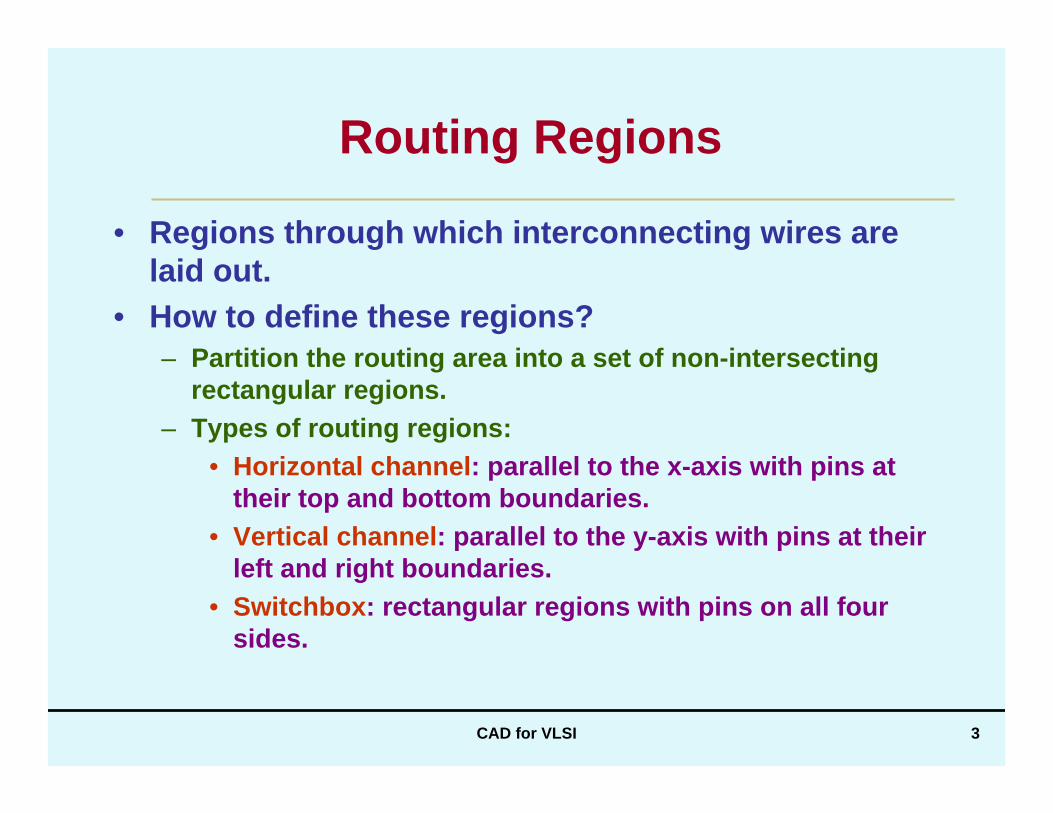
Routing Regions
• Regions through which interconnecting wires are laid out.
• How to define these regions?– Partition the routing area into a set of non-intersecting
rectangular regions.– Types of routing regions:
• Horizontal channel: parallel to the x-axis with pins at their top and bottom boundaries.
• Vertical channel: parallel to the y-axis with pins at their left and right boundaries.
• Switchbox: rectangular regions with pins on all four sides.

CAD for VLSI 4
• Points to note:– Identification of routing regions is a crucial first step to
global routing.– Routing regions often do not have pre-fixed capacities.– The order in which the routing regions are considered
during detailed routing plays a vital part in determining overall routing quality.

CAD for VLSI 5
Types of Channel Junctions
• Three types of channel junctions may occur:– L-type:
• Occurs at the corners of the layout surface.• Ordering is not important during detailed routing.• Can be routed using channel routers.
– T-type:• The leg of the “T” must be routed before the shoulder.• Can be routed using channel routers.
– +-type:• More complex and requires switchbox routers.• Advantageous to convert +-junctions to T-junctions.

CAD for VLSI 6
Illustrations
L Type T Type+ Type
CAD for VLSI 7
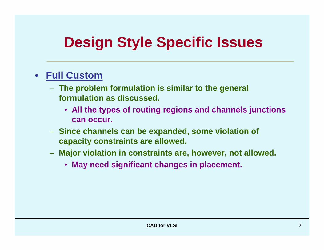
Design Style Specific Issues
• Full Custom– The problem formulation is similar to the general
formulation as discussed.• All the types of routing regions and channels junctions
can occur.– Since channels can be expanded, some violation of
capacity constraints are allowed.– Major violation in constraints are, however, not allowed.
• May need significant changes in placement.
CAD for VLSI 8
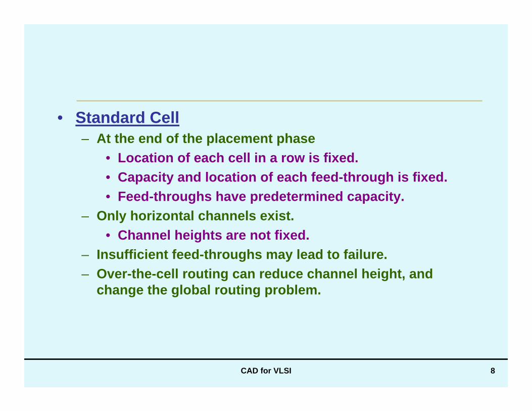
• Standard Cell– At the end of the placement phase
• Location of each cell in a row is fixed.• Capacity and location of each feed-through is fixed.• Feed-throughs have predetermined capacity.
– Only horizontal channels exist.• Channel heights are not fixed.
– Insufficient feed-throughs may lead to failure.– Over-the-cell routing can reduce channel height, and
change the global routing problem.

CAD for VLSI 9
A
B
A cannot be connected to B
CAD for VLSI 10
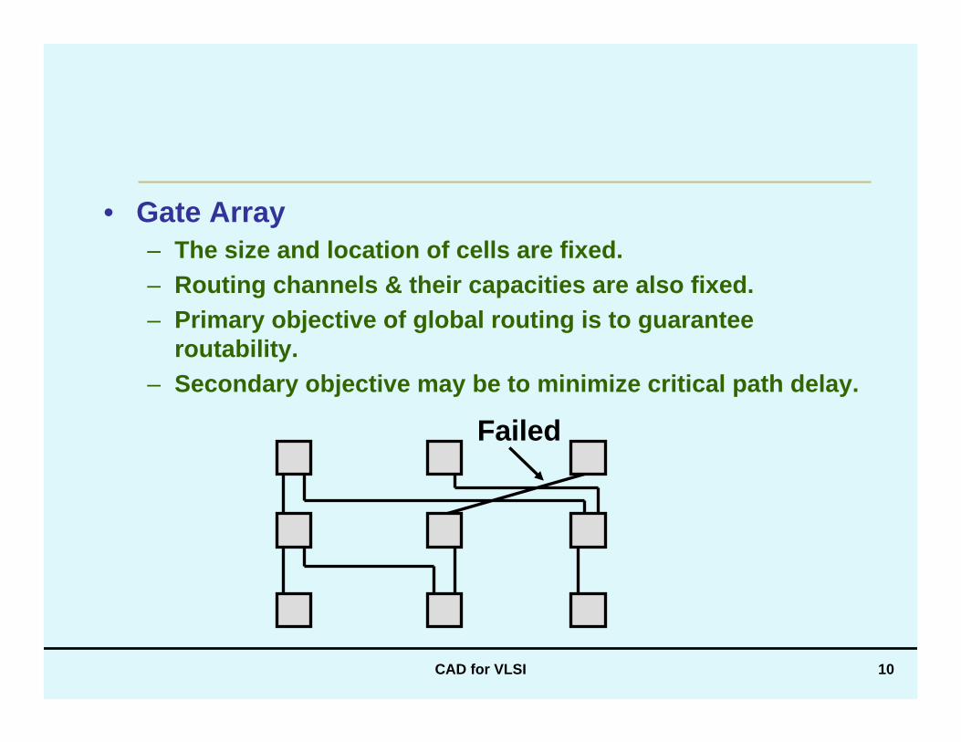
• Gate Array– The size and location of cells are fixed.– Routing channels & their capacities are also fixed.– Primary objective of global routing is to guarantee
routability.– Secondary objective may be to minimize critical path delay.
Failed
CAD for VLSI 11
Graph Models used in Global Routing
• Global routing is typically studied as a graph problem.– Routing regions and their relationships modeled as
graphs.• Three important graph models:
1. Grid Graph Model– Most suitable for area routing
2. Checker Board Model3. Channel Intersection Graph Model
– Most suitable for global routing
CAD for VLSI 12
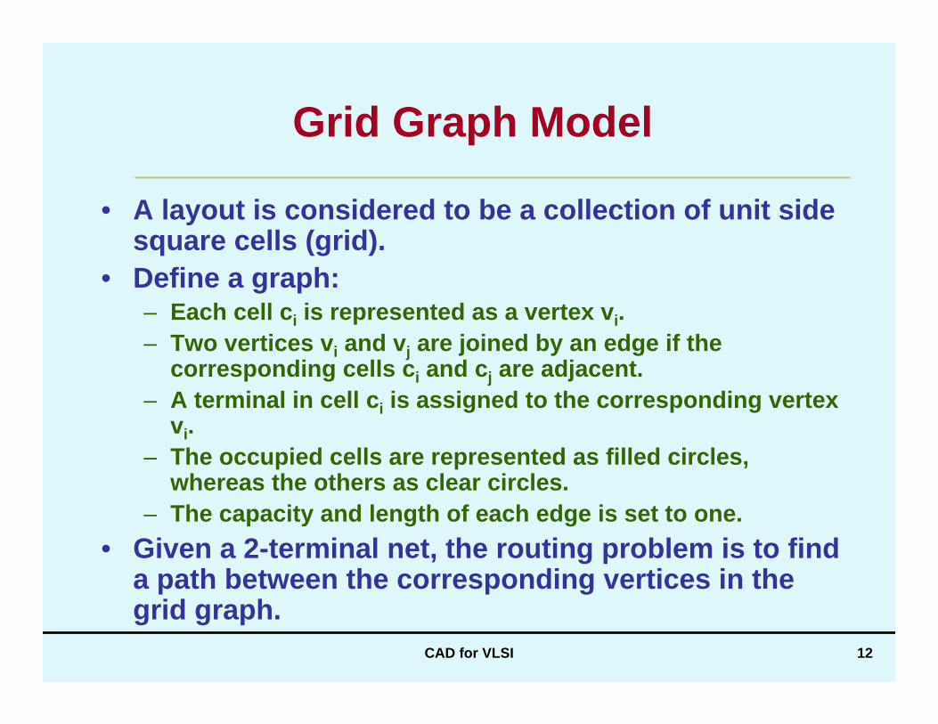
Grid Graph Model
• A layout is considered to be a collection of unit side square cells (grid).
• Define a graph:– Each cell ci is represented as a vertex vi.– Two vertices vi and vj are joined by an edge if the
corresponding cells ci and cj are adjacent.– A terminal in cell ci is assigned to the corresponding vertex
vi.– The occupied cells are represented as filled circles,
whereas the others as clear circles.– The capacity and length of each edge is set to one.
• Given a 2-terminal net, the routing problem is to find a path between the corresponding vertices in the grid graph.
CAD for VLSI 13
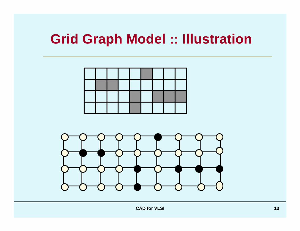
Grid Graph Model :: Illustration

CAD for VLSI 14
Checker Board Model
• More general than the grid graph model.• Approximates the layout as a coarse grid.• Checker board graph is generated in a manner
similar to the grid graph.• The edge capacities are computed based on the
actual area available for routing on the cell boundary.– The partially blocked edges have unit capacity.– The unblocked edges have a capacity of 2.
• Given the cell numbers of all terminals of a net, the global routing problem is to find a path in the coarse grid graph.

CAD for VLSI 15
Checker Board Model :: Illustration
2 1
111
111
2 1

CAD for VLSI 16
Channel Intersection Graph
• Most general and accurate model for global routing.• Define a graph:
– Each vertex vi represents a channel intersection CIi.– Channels are represented as edges.– Two vertices vi and vj are connected by an edge if there
exists a channel between CIi and CIj.– Edge weight represents channel capacity.

CAD for VLSI 17
Illustration

CAD for VLSI 18
Extended Channel Intersection Graph
• Extension of the channel intersection graph.– Includes the pins as vertices so that the connections
between the pins can be considered.• The global routing problem is simply to find a path
in the channel intersection graph.– The capacities of the edges must not be violated.– For 2-terminal nets, we can consider the nets sequentially.– For multi-terminal nets, we can have an approximation to
minimum Steiner tree.

CAD for VLSI 19
Illustration

CAD for VLSI 20
Approaches to Global Routing
• What does a global router do?– It decomposes a large routing problem into small and
manageable sub-problems • Called detailed routing
– This is done by finding a rough path for each net • Sequences of sub-regions it passes through

CAD for VLSI 21
When Floorplan is Given
• The dual graph of the floorplan (shown in red) is used for global routing.
• Each edge is assigned with:– A weight wij representing the capacity of the boundary.– A value Lij representing the edge length.
• Global routing of a two-terminal net– Terminals in rectangles r1 and r2.– Path connecting vertices v1 and v2 in G.
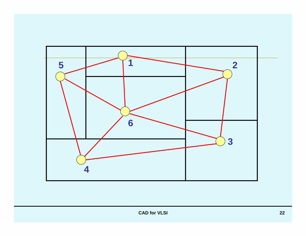
CAD for VLSI 22
6
5
3
21
4
CAD for VLSI 23
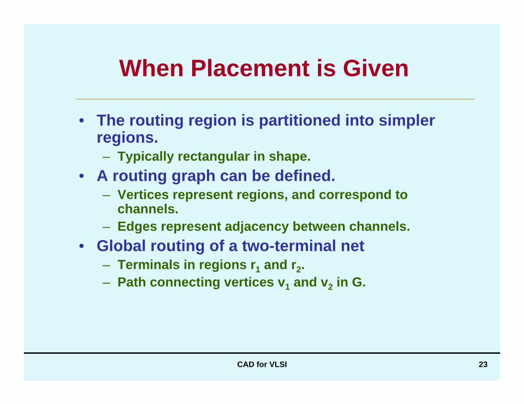
When Placement is Given
• The routing region is partitioned into simpler regions.– Typically rectangular in shape.
• A routing graph can be defined.– Vertices represent regions, and correspond to
channels.– Edges represent adjacency between channels.
• Global routing of a two-terminal net– Terminals in regions r1 and r2.– Path connecting vertices v1 and v2 in G.

CAD for VLSI 24
Sequential Approaches
• Nets are routed sequentially, one at a time.– First an ordering of the nets is obtained based on:
• Number of terminals• Bounding box length• Criticality
– Each net is then routed as dictated by the ordering.• Most of these techniques use variations of maze
running or line search methods.• Very efficient at finding routes for nets as they
employ well-known shortest path algorithms.– Rip up and reroute heuristic in case of conflict.

CAD for VLSI 25
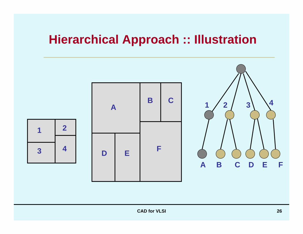
Hierarchical Approaches
• Use the hierarchy of the routing graph to decompose a large routing problem into sub-problems of manageable size.– The sub-problems are solved independently.– Sub-solutions are combined to get the total solution.
• A cut tree is defined on the routing graph.– Each interior node represents a primitive global routing
problem.– Each problem is solved optimally by translating it into an
integer programming problem.– The solutions are finally combined.
CAD for VLSI 26
Hierarchical Approach :: Illustration
F
43
21
4321
D
CBA
A
FEEDCB
CAD for VLSI 27
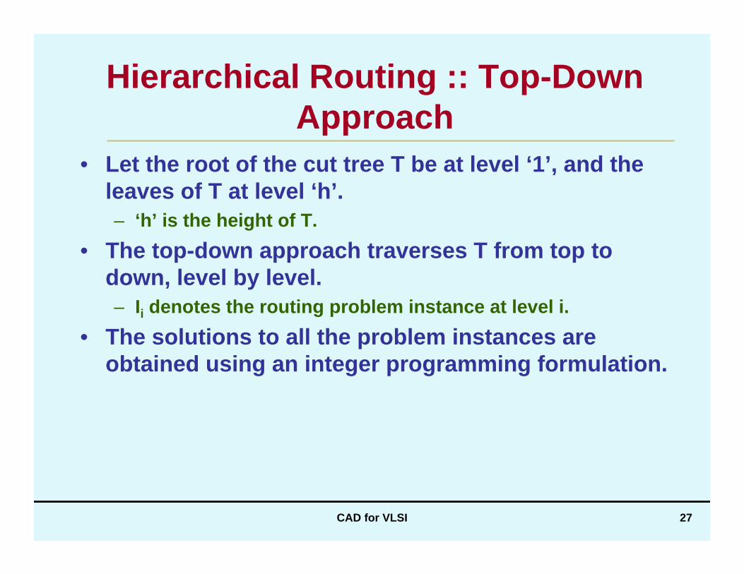
Hierarchical Routing :: Top-Down Approach
• Let the root of the cut tree T be at level ‘1’, and the leaves of T at level ‘h’.– ‘h’ is the height of T.
• The top-down approach traverses T from top to down, level by level.– Ii denotes the routing problem instance at level i.
• The solutions to all the problem instances are obtained using an integer programming formulation.

CAD for VLSI 28
Algorithm
procedure Hier_Top_Downbegin
Compute solution Ri of the routing problem I1;for i=2 to h dobegin
for all nodes n at level i-1 doCompute solution Rn of the routing problem In;Combine all solutions Rn for all nodes n, and
Ri-1 into solution Ri;end;
end.
CAD for VLSI 29
Hierarchical Routing :: Bottom-up Approach
• In the first phase, the routing problem associated with each branch in T is solved by IP.
• The partial routings are then combined by processing internal tree nodes in a bottom-up manner.
• Main disadvantage of this approach:– A global picture is obtained only in the later stages of the
process.
CAD for VLSI 30
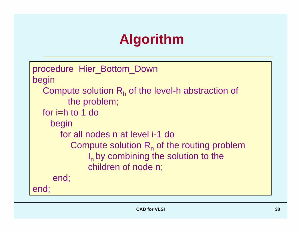
Algorithm
procedure Hier_Bottom_Downbegin
Compute solution Rh of the level-h abstraction of the problem;
for i=h to 1 dobegin
for all nodes n at level i-1 doCompute solution Rn of the routing problem
In by combining the solution to the children of node n;
end;end;

CAD for VLSI 31
Integer Linear Programming Approach
• The problem of concurrently routing the nets is computationally hard.– The only known technique uses integer programming.
• Global routing problem can be formulated as a 0/1 integer program.
• The layout is modeled as a grid graph.– N vertices: each vertex represents a grid cell.– M edges: an edge connects vertices i and j if the grid
cells i and j are adjacent.– The edge weight represents the capacity of the
boundary.
CAD for VLSI 32
Contd.
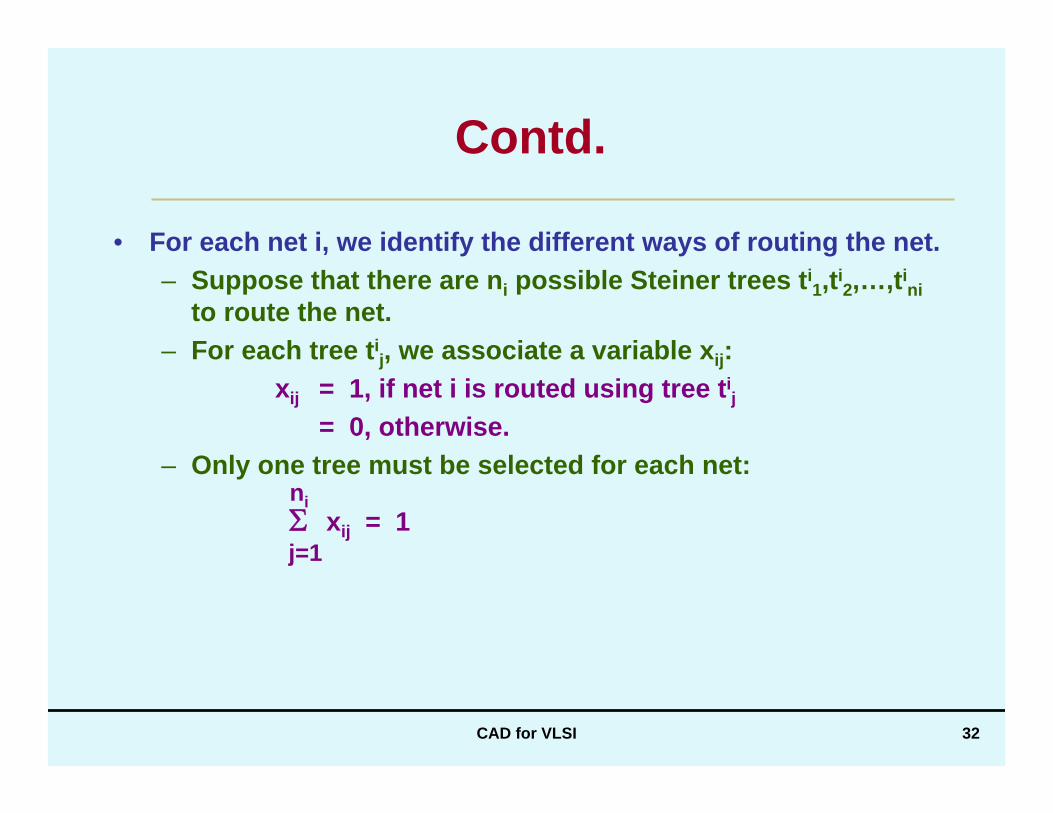
• For each net i, we identify the different ways of routing the net.– Suppose that there are ni possible Steiner trees ti
1,ti2,…,ti
nito route the net.
– For each tree tij, we associate a variable xij:
xij = 1, if net i is routed using tree tij
= 0, otherwise.– Only one tree must be selected for each net:
niΣ xij = 1j=1

CAD for VLSI 33
Contd.• For a grid graph with M edges and T = Σni trees, we can represent the
routing trees as a 0-1 matrix AMxT =[aip].aip = 1, if edge i belongs to tree p
= 0, otherwise.• Capacity of each arc (boundary) must not be exceeded:
N nkΣ Σ aip xlk ≤ ci
k=1 l=1
• If each tree tji is assigned a cost gij, then a possible objective function
to minimize is:N nk
F = Σ Σ gij xiji=1 j=1
CAD for VLSI 34
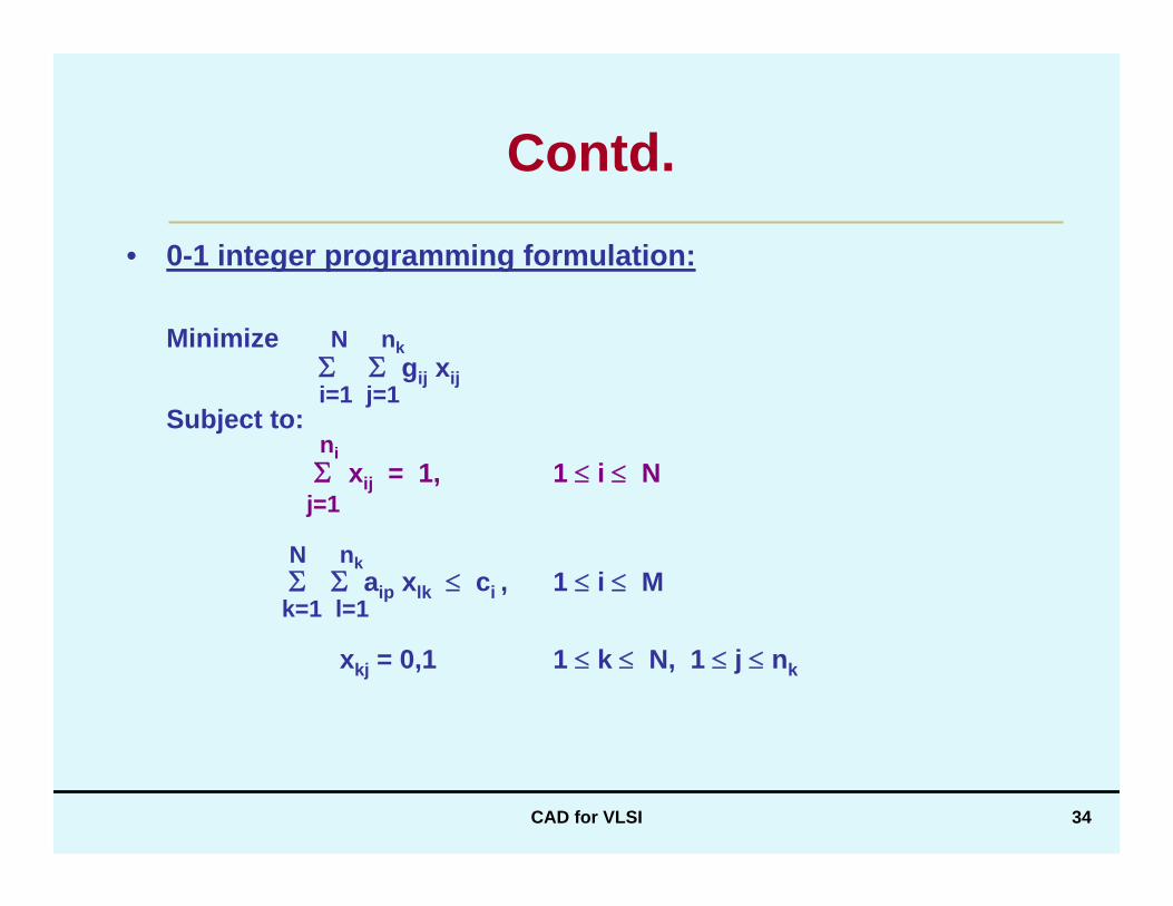
Contd.
• 0-1 integer programming formulation:
Minimize N nkΣ Σ gij xiji=1 j=1
Subject to:niΣ xij = 1, 1 ≤ i ≤ N
j=1
N nkΣ Σ aip xlk ≤ ci , 1 ≤ i ≤ M
k=1 l=1
xkj = 0,1 1 ≤ k ≤ N, 1 ≤ j ≤ nk

CAD for VLSI 35
Contd.
• General formulation.• Looks at the problem globally.• Not feasible for large input sizes.
– Time complexity increases exponentially with problem size.

CAD for VLSI 36
Performance Driven Routing
• Advent of deep sub-micron technology– Interconnect delay constitutes a significant part of the total net
delay.– Reduction in feature sizes has resulted in increased wire
resistance.– Increased proximity between the devices and interconnections
results in increased cross-talk noise.• Routers should model the cross-talk noise between adjacent
nets.• For routing high-performance circuits, techniques adopted:
– Buffer insertion– Wire sizing– High-performance topology generation