germanium‐assisted direct growth of graphene on arbitrary
TRANSCRIPT

(1 of 8) 1700929© 2017 Wiley-VCH Verlag GmbH & Co. KGaA, Weinheim www.small-journal.com
Germanium-Assisted Direct Growth of Graphene on Arbitrary Dielectric Substrates for Heating DevicesZiwen Wang, Zhongying Xue, Miao Zhang, Yongqiang Wang, Xiaoming Xie, Paul K. Chu, Peng Zhou,* Zengfeng Di,* and Xi Wang
1. Introduction
Graphene, the first stable 2D crystal, is considered to be a basic building block of other important allotropes of carbonic materials.[1] Owing to its high mobility, high conductivity, and superior mechanical properties,[2] graphene has many poten-tial applications, especially in electronic and optoelectronic devices.[3–11] In most applications, high-quality graphene needs to be transferred or directly grown on dielectric sub-strates. However, transferring the chemical vapor deposition (CVD) graphene films onto dielectric substrates inevitably introduces unintentional contamination, which degrades the physical properties through the formation of defects, impu-rities, wrinkles, cracks, or even tears.[12–14] Furthermore, in graphene-based device fabrication, transferring specific and extrinsic graphene patterns to the predesigned locations on dielectric substrates gives rise to additional technical chal-lenges. To bypass the transfer process, intense efforts have been made in an attempt to develop CVD approaches to directly grow graphene on dielectric substrates. Ismach et al. reported a pioneer metal-catalyzed transfer-free method,[15] and other modified routes have been proposed by other DOI: 10.1002/smll.201700929
Direct growth of graphene on dielectric substrates is a prerequisite to the development of graphene-based electronic and optoelectronic devices. However, the current graphene synthesis methods on dielectric substrates always involve a metal contamination problem, and the direct production of graphene patterns still remains unattainable and challenging. Herein, a semiconducting, germanium (Ge)-assisted, chemical vapor deposition approach is proposed to produce monolayer graphene directly on arbitrary dielectric substrates. By the prepatterning of a catalytic Ge layer, the graphene with desired pattern can be achieved conveniently and readily. Due to the catalysis of Ge, monolayer graphene is able to form on Ge-covered dielectric substrates including SiO2/Si, quartz glass, and sapphire substrates. Optimization of the process parameters leads to complete sublimation of the catalytic Ge layer during or immediately after formation of the monolayer graphene, enabling direct deposition of large-area and continuous graphene on dielectric substrates. The large-area, highly conductive graphene synthesized on a transparent dielectric substrate using the proposed approach has exhibited a wide range of applications, including in both defogger and thermochromic displays, as already successfully demonstrated here.
Graphene
Dr. Z. Wang, Prof. Z. Xue, Prof. M. Zhang, Prof. X. Xie, Prof. Z. Di, Prof. X. WangState Key Laboratory of Functional Materials for InformaticsShanghai Institute of Microsystem and Information TechnologyChinese Academy of Sciences865 Changning Road, Shanghai 200050, ChinaE-mail: [email protected]
Prof. Y. WangMaterials Science and Technology DivisionLos Alamos National LaboratoryLos Alamos, NM 87545, USA
Prof. P. K. ChuDepartment of Physics and Materials ScienceCity University of Hong KongTat Chee Avenue, Kowloon, Hong Kong 999077, China
Prof. P. ZhouState Key Laboratory of ASIC and SystemSchool of MicroelectronicsFudan UniversityShanghai 200433, ChinaE-mail: [email protected]
www.advancedsciencenews.com
small 2017, 13, 1700929

full papers
1700929 (2 of 8) www.small-journal.com © 2017 Wiley-VCH Verlag GmbH & Co. KGaA, Weinheim
research groups.[16–19] The graphene layers are prepared on a sacrificial metal film, followed by metal dewetting and evaporating at an elevated temperature for extended annealing time. However, metal residues are unavoidable, thus degrading the graphene properties. The successive remote metal catalyzation approach addresses the metal res-idue issue,[20,21] but the metal contamination problem, which is fatal to semiconductor devices, cannot be solved. Alterna-tively, the direct metal-catalyst-free growth of graphene on a dielectric substrate, such as Al2O3,
[22,23] Si3N4,[24,25] exfoli-
ated h-BN,[26] MgO,[27] SrTiO3,[28] SiO2,
[29–32] polydimethyl-siloxane,[33] and glass,[34,35] shows its advantages in terms of no metal contamination, but the synthesized graphene usu-ally contains substantial defects because of limited catalytic activity of the dielectric materials. Because of insufficient pyrolysis of the precursor gases, the growth process requires high temperature[22] or annealing for a long time.[25] Fur-thermore, the remote metal catalyzation technique or direct metal-catalyst-free growth method is incapable of producing graphene with the desirable patterns that are essential to gra-phene-based devices.
Germanium (Ge), which is isoelectronic to Si, has been adopted by the semiconductor industry in strain engineering since the 90-nm technology node in 2003.[36] Since then, Ge has been incorporated into every technology node to build strained Si channels, even in the current state-of-art fin field
effect transistor (FinFET) technology.[37] Here, we report metal-free Ge-assisted growth of graphene on various die-lectric substrates such as SiO2/Si, quartz glass, and sapphire. In this technique, patterned graphene can be produced on dielectric substrates easily by prepatterning the Ge film. Graphene formed on transparent dielectric substrates have demonstrated their potential in heating-device applications, including a defogger and thermochromic display, and both devices exhibit excellent performances. Given that Ge has been widely used in every recent semiconductor technology node, we believe that the graphene on dielectric substrates synthesized by the proposed strategy can expedite the prac-tical application of graphene in electronic and optoelectronic devices.
2. Results and Discussion
Figure 1a illustrates the basic concept of Ge-assisted direct growth of graphene on dielectric substrates. The 200-nm-thick Ge layer is deposited on the dielectric substrate by direct-current (DC) magnetron sputtering, and then gra-phene is produced on the Ge-coated dielectric substrate by CVD for 60–300 min at 900–930 °C (see the Experimental Section for more details).[38] As the temperature is close to the melting point of Ge, the Ge catalyst layer is evaporated
www.advancedsciencenews.com
small 2017, 13, 1700929
Figure 1. a) Schematic illustration of Ge-assisted direct growth of graphene on arbitrary dielectric substrates. b) Photograph of SiO2/Si, quartz glass, and sapphire substrates before and after graphene growth. The yellow boxes are drawn to state the regions of interest. c) Raman scattering spectra of the graphene covered SiO2/Si, quartz glass, and sapphire substrates. d) Optical microscopy image of the prepatterned Ge layer on the SiO2/Si substrate. e) Optical microscopy image of the graphene pattern on the SiO2/Si substrate. f) Raman intensity mapping of the 2D peak of the graphene pattern on the SiO2/Si substrate shown in (e).

(3 of 8) 1700929© 2017 Wiley-VCH Verlag GmbH & Co. KGaA, Weinheim www.small-journal.com
gradually during the graphene growth. By optimizing the conditions, the formation of continuous graphene and the evaporation of the entire Ge layer can be accomplished simultaneously to form graphene on the dielectric substrate directly. Figure 1b displays the images of the pristine and gra-phene-coated dielectric substrates, including SiO2/Si, quartz glass, and sapphire, and a uniform color indicates good gra-phene uniformity. The graphene films on different dielectric substrates are characterized by Raman scattering, as shown in Figure 1c. The characteristic peaks of graphene at D, G, and 2D bands can be observed,[39] but that of the Ge layer is not observed (not shown), indicating the direct growth of graphene on three dielectric substrates with the complete evaporation of the Ge layer. The ratios of the 2D peak to G peak (I2D/IG) of graphene on SiO2/Si, quartz glass, and sap-phire are 1.43, 1.76, and 1.69, respectively. Furthermore, the 2D peak for each graphene covered dielectric substrate pos-sesses a symmetric shape with one single Lorentzian profile (Figure S1, Supporting Information). Therefore, it is con-cluded that the synthesized graphene on dielectric substrates is monolayered.[40] The UV–vis transmittance spectra further confirm the synthesis of monolayered graphene, as shown in Figure S2 (Supporting Information).[41] In addition to the large-scale continuous graphene, graphene patterns—the
essential building blocks in graphene-based electronic and optoelectronic devices—can be prepared directly by this technique. By prepatterning of the Ge layer (Figure 1d), gra-phene islands with the same pattern can be grown on the SiO2/Si substrate, as shown in Figure 1e. The corresponding color-coded intensity mapping of the 2D peak (Figure 1f) suggests that the graphene pattern has good uniformity. Meanwhile, graphene islands with arbitrary patterns can be obtained by our approach, as shown in Figure S3 (Supporting Information).
To elucidate the mechanism of Ge-assisted direct growth of graphene on dielectric substrates, the effects of the growth time and temperature are studied, as shown in Figures 2 and 3. Scanning electron microscopy (SEM) (Figure 2a1–e1), integrated Raman intensity mapping of the Ge peak (Figure 2a2–e2), and energy-dispersive X-ray spectroscopy mapping (Figure S4 and Table S1, Supporting Information) are performed to monitor the evolution of the Ge layer. Dewetting and evap-oration occur as the graphene layer starts to grow. The Ge layer breaks into fragments, but interconnected Ge areas still exist after 60 min. The interconnected Ge areas further evolve into fingerlike structures after 120 min, similar to that observed from Cu films previously.[15] The Ge layer is entirely evaporated after 300 min of CVD growth. Gradual
www.advancedsciencenews.com
small 2017, 13, 1700929
Figure 2. Evolution of Ge evaporation and graphene formation with CVD time. a1–e1) Optical images of graphene grown on SiO2/Si at 920 °C for different times. Scale bar: 20 µm. a2–e2) Raman mappings of the Ge peak intensity as a function of growth time. The mapped areas are selected in (a1–e1) as denoted by dashed yellow squares. Scale bar: 10 µm. a3–e3) Raman mappings of the I2D/IG ratio of graphene. Scale bar: 10 µm. f) Raman spectra of Ge for different CVD times at 920 °C. g) Raman spectra of graphene for different CVD times at 920 °C. f) and g) are measured from the color dots marked in (a1–e1). h) Statistical I2D/IG and ID/IG ratios as a function of time, each data point comes from the statistical result of the corresponding Raman mappings.
full papers
1700929 (4 of 8) www.small-journal.com © 2017 Wiley-VCH Verlag GmbH & Co. KGaA, Weinheim
removal of the Ge layer by evaporation is also confirmed by the Raman scattering spectra (Figure 2f) acquired from the selected areas shown in Figure 2a1–e1. Figure 2f also suggests that even in the regions between the fingerlike structures, there is Ge signal in the initial stage (60–180 min), but the residual Ge evaporates completely after 240 min, as shown by the disappearance of the associated Ge Raman peak at 300.4 cm−1, whereas a new Raman peak corresponding to Si substrate appears at 303 cm−1. The existence of Ge either in the fingerlike structure or beyond the finger area causes strong absorption and scattering of the excitation laser, and therefore, the intensity of the characteristic Raman peaks corresponding to the graphene overlayer is attenuated con-siderably, as shown in Figure S5 (Supporting Information). In other words, the scanning Raman image of a 2D band of graphene is closely related to the amount of residual Ge (Figure S6, Supporting Information), and only the mapping of I2D/IG ratio can avoid the influence from Ge residual on SiO2/Si substrate, thus revealing the distribution of the grown graphene (Figure 2a3–e3). The graphene becomes more
uniform as residual Ge evaporates gradually with time. For the growth time less than 300 min, the crystalline quality of graphene is also improved with the prolonged growth time, as suggested by the raw Raman data (Figure 2g) together with the increased I2D/IG ratio and the decreased ID/IG ratio shown in Figure 2h. It should be noted that the crystal-line quality of graphene will not significantly change as the growth time is extended for more than 300 min (Figure S7, Supporting Information), indicating that Ge catalyst layer has been evaporated completely and the continuous gra-phene layer has formed after 300 min.
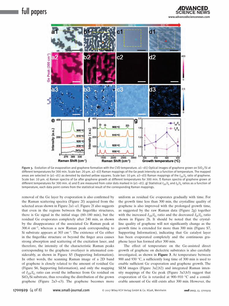
The effect of temperature on the Ge-assisted direct growth of graphene on dielectric substrates is also carefully investigated, as shown in Figure 3. At temperature between 900 and 930 °C, a sufficiently long time of 300 min is used to enable sufficient Ge evaporation and graphene growth. The SEM images (Figure 3a2,b2) and integrated Raman inten-sity mappings of the Ge peak (Figure 3a3,b3) suggest that evaporation of Ge is retarded at 900–910 °C and a consid-erable amount of Ge still exists after 300 min. However, the
www.advancedsciencenews.com
small 2017, 13, 1700929
Figure 3. Evolution of Ge evaporation and graphene formation with the CVD temperature. a1–d1) Optical images of graphene grown on SiO2/Si at different temperatures for 300 min. Scale bar: 20 µm. a2–d2) Raman mappings of the Ge peak intensity as a function of temperature. The mapped areas are selected in (a1–d1) as denoted by dashed yellow squares. Scale bar: 10 µm. a3–d3) Raman mappings of the I2D/IG ratio of graphene. Scale bar: 10 µm. e) Raman spectra of Ge after graphene growth at different temperatures for 300 min. f) Raman spectra of graphene grown at different temperatures for 300 min. e) and f) are measured from color dots marked in (a1–d1). g) Statistical I2D/IG and ID/IG ratios as a function of temperature, each data point comes from the statistical result of the corresponding Raman mappings.

(5 of 8) 1700929© 2017 Wiley-VCH Verlag GmbH & Co. KGaA, Weinheim www.small-journal.com
evaporation rate of Ge increases at 920–930 °C and the Ge layer is entirely evaporated after 300 min CVD growth. Sim-ilar conclusions can be drawn from the raw Raman data in Figure 3e. With regard to the graphene fabricated at 930 °C, the evaporation rate of Ge is too large for the formation of a continuous graphene layer and so only graphene fragments are produced prior to complete evaporation of Ge, as shown in Figure 3d1–d3. With respect to the graphene grown at a temperature lower than 930 °C, the graphene layer with con-tinuous coverage is formed, but the uniformity is better at a higher growth temperature, as shown by Figure 3a3–c3. In addition, the crystalline quality of the synthesized graphene becomes better for relatively high temperatures, as suggested by Raman spectra shown in Figure 3f, besides larger I2D/IG and smaller of ID/IG in Figure 3g. It is concluded that 920 °C is the optimal temperature for the growth of high-quality continuous graphene on dielectric substrates.
Figure 4 shows the detailed structural characteriza-tion of the graphene prepared on a SiO2/Si substrate at 920 °C for 300 min. Prior to graphene growth, the Ge 3d5 peak originates from the Ge layer, and the high-resolution C 1s spectrum (left inset in Figure 4a) only consists of the carbon sp3-hybridization peak at 285.4 eV arising from natural carbon contamination. After deposition of the con-tinuous graphene layer, the Ge 3d5 peak disappears and the intensity of the C 1s peak increases. The high-resolu-tion C 1s signal (right inset in Figure 4a) indicates that the sp3-related peak recedes as a clear sharp carbon sp2-hybridization peak at 284.0 eV emerges, indicative of the formation of the sp2 network, i.e., graphene. The crystal-lographic information is provided by transmission electron microscopy (TEM) and selected-area electron diffraction
(SAED). The high-resolution TEM (HR-TEM) (Figure 4d) image acquired from the crack edge of the graphene film (Figure 4c) exhibits single layer characteristics. The SAED pattern (Figure 4e) shows multiple sets of spots with hexag-onal distributions, indicating the formation of polycrystalline graphene consisting of multiple grains. Figure 4f shows the light intensity of the four spots marked by the dashed box in Figure 4e. The intensity ratio (outermost to innermost) of ≈1:2 suggests the formation of monolayer graphene. A back-gated graphene FET (GFET) device is fabricated to evaluate the transport properties of the monolayer graphene. The schematic structure and typical transfer curve (IDS–VG) measured at room temperature under ambient conditions are shown in Figure 4b and Figure S8 (Supporting Infor-mation), respectively. The transfer curve acquired at VDS of 100 mV shows that both hole and electron conduction can be achieved by gating. The Dirac point of the GFET is at a positive gate voltage of VG = 11.2 V, suggesting that the gra-phene is p-doped due to possible water/oxygen adsorption. The extracted field-effect hole and electron mobilities at room temperature are determined to be µh = 730 cm2 V−1 s−1 and µe = 570 cm2 V−1 s−1, respectively, which are comparable to the carrier mobilities of the graphene grown on SiO2 by catalytic Cu.[42]
To explore potential applications of the continuous con-ductive graphene on dielectric substrates, heating devices are fabricated using the graphene grown on a quartz glass substrate. Transparent graphene heating devices have been demonstrated in defogging applications, schematically illus-trated in Figure 5a. When the transparent graphene heater is placed above a beaker containing half a cup of hot water, the surface is quickly covered by fog. As a bias of 20 V is
www.advancedsciencenews.com
small 2017, 13, 1700929
Figure 4. Characterization of monolayer graphene directly grown on SiO2/Si by Ge-assisted growth. a) XPS analysis of the SiO2/Si substrate before and after graphene growth. The insets depict the corresponding C 1s peak. b) Transfer characteristics (IDS–VG) of the graphene transistor at VDS = 100 mV. Inset: Schematic image of the fabricated GFET device. c) Low-magnification TEM image of the graphene transferred onto the copper grid. d) HR-TEM image of the graphene edge. e) SAED pattern of graphene. f) Profiles of diffraction spot intensities along the dashed box in (e).
full papers
1700929 (6 of 8) www.small-journal.com © 2017 Wiley-VCH Verlag GmbH & Co. KGaA, Weinheim
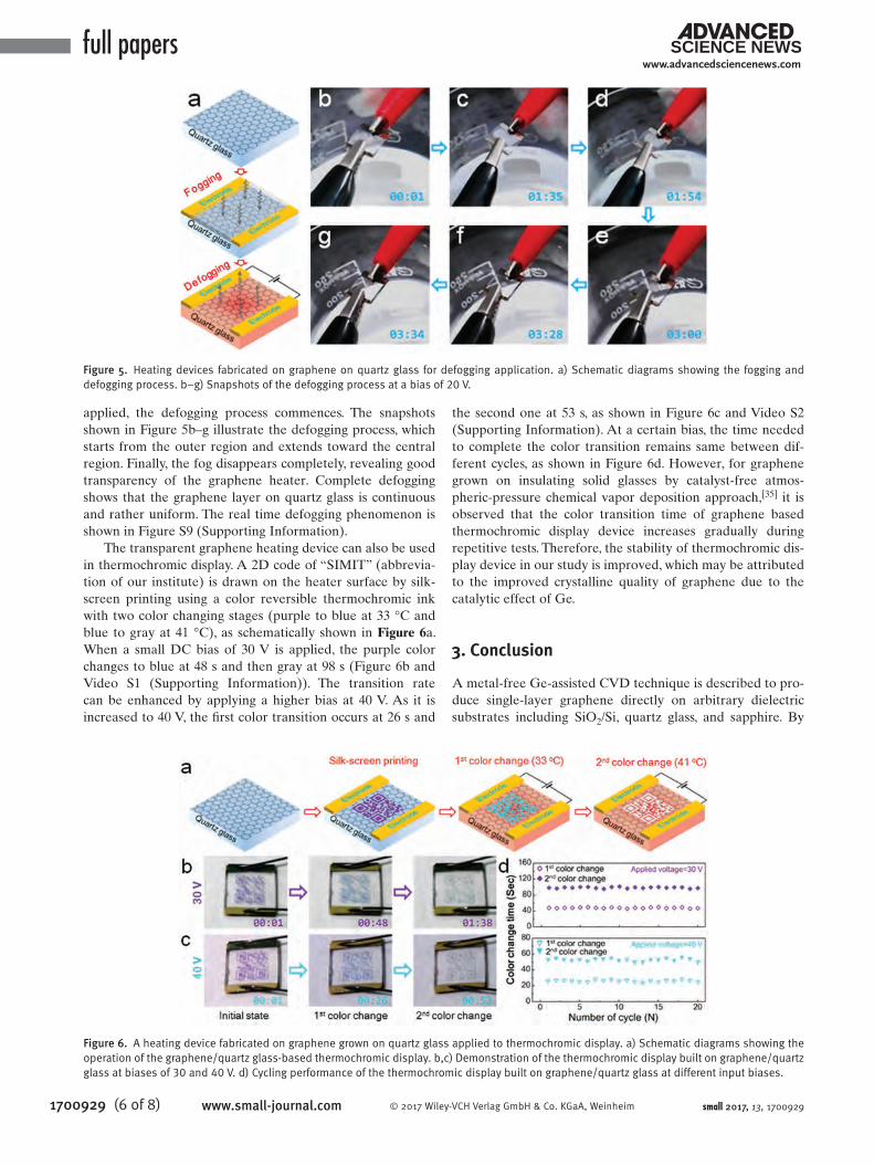
applied, the defogging process commences. The snapshots shown in Figure 5b–g illustrate the defogging process, which starts from the outer region and extends toward the central region. Finally, the fog disappears completely, revealing good transparency of the graphene heater. Complete defogging shows that the graphene layer on quartz glass is continuous and rather uniform. The real time defogging phenomenon is shown in Figure S9 (Supporting Information).
The transparent graphene heating device can also be used in thermochromic display. A 2D code of “SIMIT” (abbrevia-tion of our institute) is drawn on the heater surface by silk-screen printing using a color reversible thermochromic ink with two color changing stages (purple to blue at 33 °C and blue to gray at 41 °C), as schematically shown in Figure 6a. When a small DC bias of 30 V is applied, the purple color changes to blue at 48 s and then gray at 98 s (Figure 6b and Video S1 (Supporting Information)). The transition rate can be enhanced by applying a higher bias at 40 V. As it is increased to 40 V, the first color transition occurs at 26 s and
the second one at 53 s, as shown in Figure 6c and Video S2 (Supporting Information). At a certain bias, the time needed to complete the color transition remains same between dif-ferent cycles, as shown in Figure 6d. However, for graphene grown on insulating solid glasses by catalyst-free atmos-pheric-pressure chemical vapor deposition approach,[35] it is observed that the color transition time of graphene based thermochromic display device increases gradually during repetitive tests. Therefore, the stability of thermochromic dis-play device in our study is improved, which may be attributed to the improved crystalline quality of graphene due to the catalytic effect of Ge.
3. Conclusion
A metal-free Ge-assisted CVD technique is described to pro-duce single-layer graphene directly on arbitrary dielectric substrates including SiO2/Si, quartz glass, and sapphire. By
www.advancedsciencenews.com
small 2017, 13, 1700929
Figure 5. Heating devices fabricated on graphene on quartz glass for defogging application. a) Schematic diagrams showing the fogging and defogging process. b–g) Snapshots of the defogging process at a bias of 20 V.
Figure 6. A heating device fabricated on graphene grown on quartz glass applied to thermochromic display. a) Schematic diagrams showing the operation of the graphene/quartz glass-based thermochromic display. b,c) Demonstration of the thermochromic display built on graphene/quartz glass at biases of 30 and 40 V. d) Cycling performance of the thermochromic display built on graphene/quartz glass at different input biases.

(7 of 8) 1700929© 2017 Wiley-VCH Verlag GmbH & Co. KGaA, Weinheim www.small-journal.com
www.advancedsciencenews.com
small 2017, 13, 1700929
optimizing the time and the temperature, the Ge evaporates completely during or immediately after formation of the monolayer graphene, thus resulting in the direct deposition of large-area and continuous graphene on dielectric substrates without metal contamination. The graphene synthesized on a transparent quartz glass is suitable for heating applications such as defogging and thermochromic displays. This prom-ising technique for direct synthesis of graphene on dielectric substrates without metallic contamination may pave the way for the implementation of graphene for electronic and opto-electronic device application.
4. Experimental Section
Direct Growth of Graphene on Dielectric Substrates: DC mag-netron sputtering (JGMF 500) was used to deposit 200-nm-thick Ge films on dielectric substrates (highly doped p-Si substrates with a 300-nm-thick thermal oxide layer, quartz glass, and sap-phire). The samples were loaded in a tube furnace. After pumping down to 10−4 mbar, the pump was turned off and a mixture of hydrogen (23 sccm) and argon (230 sccm) was introduced until reaching atmospheric pressure. Without changing the gas flow rates, the samples were heated to 900–930 °C, which was close to the melting point of Ge. Graphene fabrication was carried out by adding methane (0.7 sccm) for 60–360 min. Afterward, the system was cooled to room temperature at a rate of 10 °C min−1.
Transfer of Graphene: To characterize the quality and layer numbers of the graphene by TEM, it was necessary to transfer it to a copper grid. The TEM sample preparation was performed using a polymethylmethacrylate(PMMA)-assisted transfer method, as schematically shown in Figure S10 (Supporting Information). A thin film of PMMA was spin-coated onto the graphene/SiO2/Si and baked at 100 °C for 10 min. It was immersed in a NaOH solution (100 mL and 10 wt%). Owing to the existence of PMMA, the sample floated on the surface of the solution. After immersing for 12 h, the silicon dioxide layer was completely etched by NaOH and the PMMA/graphene film was detached from the Si substrate while the Si substrate sank to the bottom of the solution. After the PMMA/graphene film was rinsed with deionized water sev-eral times, it was loaded onto a TEM copper grid and annealed at 100 °C for 10 min to improve adhesion. Finally, the PMMA was dissolved in hot acetone at 80 °C.
Characterization: The graphene/dielectric samples were char-acterized by Raman scattering (HORIBA Jobin Yvon HR800) using an Ar+ laser with a wavelength of 514 nm and a spot size of 1 µm, SEM (Zeiss Gemini Ultra-55), X-ray photoelectron spectroscopy (XPS; PHI 5802, Physical Electronics Inc., Eden Prairie, MN), TEM (FET-Tecnai G2F20 S-7WIN), and atomic force microscopy (Bruker Multimode 8).
Electrical Measurements: The back-gated GFETs were fabri-cated with the graphene/SiO2/Si. The source and drain electrodes (50-nm Au/10-nm Ti) were deposited by electron beam evapo-ration and a photolithographic step employing an inductively coupled plasma was used to pattern the graphene to form a field-effect transistor with a channel length of 8 µm and width of 2 µm. To improve the contact of the back-gated GFET device, annealing was performed in Ar (500 sccm) and H2 (10 sccm) at 300 °C for 8 h in a tube furnace. The back-gated GFETs were characterized under
ambient conditions using the Agilent (B1500A) semiconductor parameter analyzer. The mobility was extracted using the following equation:
IV
LW C V
ddFET
DS
G ox DSµ = ⋅ ⋅ ⋅ (1)
where L and W are the channel length and width, respectively, Cox is the gate oxide capacitance (11 nF cm−2), VDS is the source drain voltage, IDS is the source drain current, and VG is the gate voltage. The linear regime of the transfer characteristics was used to obtain dIDS/dVG.
Supporting Information
Supporting Information is available from the Wiley Online Library or from the author.
Acknowledgements
Z.W. and Z.X. contributed equally to this work. The authors thank the Program of Shanghai Academic/Technology Research Leader (16XD1404200), the Key Research Project of Frontier Sci-ence, Chinese Academy of Sciences (QYZDB-SSW-JSC021), and the City University of Hong Kong Applied Research Grant (ARG) No. 9667122 for financial support. Partial support was also pro-vided by the Center for Integrated Nanotechnologies (CINT), a US DOE nanoscience user facility jointly operated by Los Alamos and Sandia National Laboratories.
Conflict of Interest
The authors declare no conflict of interest.
[1] A. K. Geim, K. S. Novoselov, Nat. Mater. 2007, 6, 183.[2] K. S. Novoselov, D. Jiang, F. Schedin, T. J. Booth, V. V. Khotkevich,
S. V. Morozov, A. K. Geim, Proc. Natl. Acad. Sci. USA 2005, 102, 10451.
[3] J. Du, H.-M. Cheng, Macromol. Chem. Phys. 2012, 213, 1060.[4] E. Yoo, J. Kim, E. Hosono, H.-S. Zhou, T. Kudo, I. Honma, Nano Lett.
2008, 8, 2277.[5] T. Lin, I.-W. Chen, F. Liu, C. Yang, H. Bi, F. Xu, F. Huang, Science
2015, 350, 1508.[6] S. Bae, H. Kim, Y. Lee, X. Xu, J.-S. Park, Y. Zheng, J. Balakrishnan,
T. Lei, H. Ri Kim, Y. I. Song, Y.-J. Kim, K. S. Kim, B. Ozyilmaz, J.-H. Ahn, B. H. Hong, S. Iijima, Nat. Nanotechnol. 2010, 5, 574.
[7] L. Ju, B. Geng, J. Horng, C. Girit, M. Martin, Z. Hao, H. A. Bechtel, X. Liang, A. Zettl, Y. R. Shen, F. Wang, Nat. Nanotechnol. 2011, 6, 630.
[8] Y.-M. Lin, C. Dimitrakopoulos, K. A. Jenkins, D. B. Farmer, H.-Y. Chiu, A. Grill, P. Avouris, Science 2010, 327, 662.
[9] F. Schedin, A. K. Geim, S. V. Morozov, E. W. Hill, P. Blake, M. I. Katsnelson, K. S. Novoselov, Nat. Mater. 2007, 6, 652.
[10] Y. Ohno, K. Maehashi, Y. Yamashiro, K. Matsumoto, Nano Lett. 2009, 9, 3318.
[11] X. Li, X. Wang, L. Zhang, S. Lee, H. Dai, Science 2008, 319, 1229.

full papers
1700929 (8 of 8) www.small-journal.com © 2017 Wiley-VCH Verlag GmbH & Co. KGaA, Weinheim
www.advancedsciencenews.com
small 2017, 13, 1700929
[12] X. Li, Y. Zhu, W. Cai, M. Borysiak, B. Han, D. Chen, R. D. Piner, L. Colombo, R. S. Ruoff, Nano Lett. 2009, 9, 4359.
[13] Y.-C. Lin, C. Jin, J.-C. Lee, S.-F. Jen, K. Suenaga, P.-W. Chiu, ACS Nano 2011, 5, 2362.
[14] Y.-C. Lin, C.-C. Lu, C.-H. Yeh, C. Jin, K. Suenaga, P.-W. Chiu, Nano Lett. 2012, 12, 414.
[15] A. Ismach, C. Druzgalski, S. Penwell, A. Schwartzberg, M. Zheng, A. Javey, J. Bokor, Y. Zhang, Nano Lett. 2010, 10, 1542.
[16] H.-J. Shin, W. M. Choi, S.-M. Yoon, G. H. Han, Y. S. Woo, E. S. Kim, S. J. Chae, X.-S. Li, A. Benayad, D. D. Loc, F. Gunes, Y. H. Lee, J.-Y. Choi, Adv. Mater. 2011, 23, 4392.
[17] J. Hofrichter, B. N. Szafranek, M. Otto, T. J. Echtermeyer, M. Baus, A. Majerus, V. Geringer, M. Ramsteiner, H. Kurz, Nano Lett. 2010, 10, 36.
[18] T. Kato, R. Hatakeyama, ACS Nano 2012, 6, 8508.[19] Q.-Q. Zhuo, Q. Wang, Y.-P. Zhang, D. Zhang, Q.-L. Li, C.-H. Gao,
Y.-Q. Sun, L. Ding, Q.-J. Sun, S.-D. Wang, J. Zhong, X.-H. Sun, S.-T. Lee, ACS Nano 2015, 9, 594.
[20] P.-Y. Teng, C.-C. Lu, K. Akiyama-Hasegawa, Y.-C. Lin, C.-H. Yeh, K. Suenaga, P.-W. Chiu, Nano Lett. 2012, 12, 1379.
[21] H. Kim, I. Song, C. Park, M. Son, M. Hong, Y. Kim, J. S. Kim, H.-J. Shin, J. Baik, H. C. Choi, ACS Nano 2013, 7, 6575.
[22] J. Hwang, M. Kim, D. Campbell, H. A. Alsalman, J. Y. Kwak, S. Shivaraman, A. R. Woll, A. K. Singh, R. G. Hennig, S. Gorantla, M. H. Rümmeli, M. G. Spencer, ACS Nano 2013, 7, 385.
[23] H. J. Song, M. Son, C. Park, H. Lim, M. P. Levendorf, A. W. Tsen, J. Park, H. C. Choi, Nanoscale 2012, 4, 3050.
[24] J. Chen, Y. Guo, Y. Wen, L. Huang, Y. Xue, D. Geng, B. Wu, B. Luo, G. Yu, Y. Liu, Adv. Mater. 2013, 25, 992.
[25] J. Chen, Y. Guo, L. Jiang, Z. Xu, L. Huang, Y. Xue, D. Geng, B. Wu, W. Hu, G. Yu, Y. Liu, Adv. Mater. 2014, 26, 1348.
[26] M. Son, H. Lim, M. Hong, H. C. Choi, Nanoscale 2011, 3, 3089.[27] M. H. Rümmeli, A. Bachmatiuk, A. Scott, F. Börrnert, J. H. Warner,
V. Hoffman, J.-H. Lin, G. Cuniberti, B. Büchner, ACS Nano 2010, 4, 4206.
[28] J. Sun, T. Gao, X. Song, Y. Zhao, Y. Lin, H. Wang, D. Ma, Y. Chen, W. Xiang, J. Wang, Y. Zhang, Z. Liu, J. Am. Chem. Soc. 2014, 136, 6574.
[29] J. Kwak, J. H. Chu, J.-K. Choi, S.-D. Park, H. Go, S. Y. Kim, K. Park, S.-D. Kim, Y.-W. Kim, E. Yoon, S. Kodambaka, S.-Y. Kwon, Nat. Commun. 2012, 3, 645.
[30] Q. F. Liu, Y. P. Gong, T. Wang, W. L. Chan, J. Wu, Carbon 2016, 96, 203.
[31] J. B. Pang, R. G. Mendes, P. S. Wrobel, M. D. Wlodarski, H. Q. Ta, L. Zhao, L. Giebeler, B. Trzebicka, T. Gemming, L. Fu, Z. F. Liu, J. Eckert, A. Bachmatiuk, M. H. Rummeli, ACS Nano 2017, 11, 1946.
[32] R. Muñoz, C. Munuera, J. I. Martínez, J. Azpeitia, C. Gómez-Aleixandre, M. García-Hernández, 2D Mater. 2017, 4, 015009.
[33] H. K. Seo, K. Kim, S. Y. Min, Y. Lee, C. E. Park, R. Raj, T. W. Lee, 2D Mater. 2017, 4, 024001.
[34] X. D. Chen, Z. L. Chen, W. S. Jiang, C. H. Zhang, J. Y. Sun, H. H. Wang, W. Xin, L. Lin, M. K. Priydarshi, H. Yang, Z. B. Liu, J. G. Tian, Y. Y. Zhang, Y. F. Zhang, Z. F. Liu, Adv. Mater. 2017, 29, 1603428.
[35] J. Sun, Y. Chen, M. K. Priydarshi, Z. Chen, A. Bachmatiuk, Z. Zou, Z. Chen, X. Song, Y. Gao, M. H. Rümmeli, Y. Zhang, Z. Liu, Nano Lett. 2015, 15, 5846.
[36] T. Ghani, M. Armstrong, C. Auth, M. Bost, P. Charvat, G. Glass, T. Hoffmann, K. Johnson, C. Kenyon, J. Klaus, B. McIntyre, K. Mistry, A. Murthy, J. Sandford, M. Silberstein, S. Sivakumar, P. Smith, K. Zawadzki, S. Thompson, M. Bohr, IEDM Tech. Dig. 2003, 2003, 978.
[37] C. Auth, C. Allen, A. Blattner, D. Bergstrom, M. Brazier, M. Bost, M. Buehler, V. Chikarmane, T. Ghani, T. Glassman, R. Grover, W. Han, D. Hanken, M. Hattendorf, P. Hentges, R. Heussner, J. Hicks, D. Ingerly, P. Jain, S. Jaloviar, R. James, D. Jones, J. Jopling, S. Joshi, C. Kenyon, H. Liu, R. McFadden, B. McIntyre, J. Neirynck, C. Parker, L. Pipes, I. Post, S. Pradhan, M. Prince, S. Ramey, T. Reynolds, J. Roesler, J. Sandford, J. Seiple, P. Smith, C. Thomas, D. Towner, T. Troeger, C. Weber, P. Yashar, K. Zawadzki, K. Mistry, Symp. VLSI Tech. Dig. 2012, 131.
[38] G. Wang, M. Zhang, Y. Zhu, G. Ding, D. Jiang, Q. Guo, S. Liu, X. Xie, P. K. Chu, Z. Di, X. Wang, Sci. Rep. 2013, 3, 2465.
[39] A. C. Ferrari, D. M. Basko, Nat. Nanotechnol. 2013, 8, 235.[40] X. Li, W. Cai, J. An, S. Kim, J. Nah, D. Yang, R. Piner,
A. Velamakanni, I. Jung, E. Tutuc, S. K. Banerjee, L. Colombo, R. S. Ruoff, Science 2009, 324, 1312.
[41] R. R. Nair, P. Blake, A. N. Grigorenko, K. S. Novoselov, T. J. Booth, T. Stauber, N. M. R. Peres, A. K. Geim, Science 2008, 320, 1308.
[42] C.-Y. Su, A.-Y. Lu, C.-Y. Wu, Y.-T. Li, K.-K. Liu, W. Zhang, S.-Y. Lin, Z.-Y. Juang, Y.-L. Zhong, F.-R. Chen, L.-J. Li, Nano Lett. 2011, 11, 3612.
Received: March 21, 2017Revised: April 12, 2017Published online: May 31, 2017

Copyright WILEY-VCH Verlag GmbH & Co. KGaA, 69469 Weinheim, Germany, 2017.
Supporting Information
for Small, DOI: 10.1002/smll.201700929
Germanium-Assisted Direct Growth of Graphene on ArbitraryDielectric Substrates for Heating Devices
Ziwen Wang, Zhongying Xue, Miao Zhang, Yongqiang Wang,Xiaoming Xie, Paul K. Chu, Peng Zhou,* Zengfeng Di,* andXi Wang

Supplementary Information
Germanium-assisted Direct Growth of Graphene on Arbitrary Dielectric
Substrates for Heating Devices
Ziwen Wang, Zhongying Xue, Miao Zhang, Yongqiang Wang, Xiaoming Xie, Paul K.
Chu, Peng Zhou,* Zengfeng Di,* and Xi Wang
Figure S1. Raman 2D-peak Lorentzian fitting of the as-grown graphene on a) 300 nm
SiO2/Si, b) sapphire, and c) quartz glass. All the symmetric 2D peaks can be well
fitted with a single Lorentzian curve, which proves that the as-synthesized graphene
on a dielectric substrate is monolayered.

Figure S2. UV−vis transmittance spectra of quartz glass before and after graphene
growth. At a wavelength of 550 nm, the graphene absorptivity is ~2.7%, which is
consistent with the theoretical value of monolayer graphene.
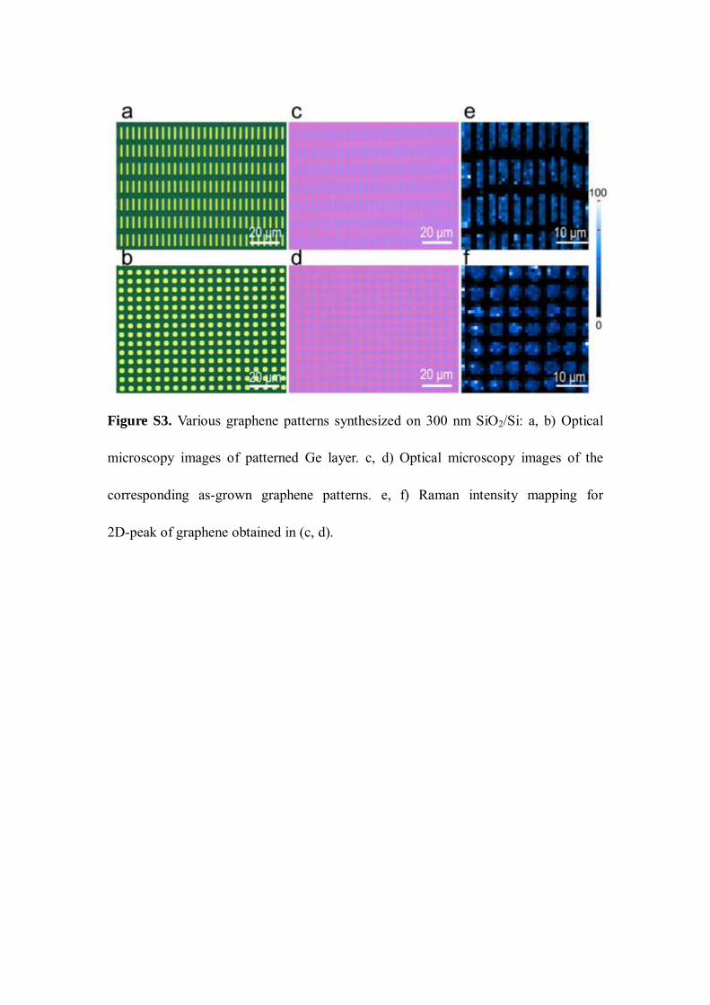
Figure S3. Various graphene patterns synthesized on 300 nm SiO2/Si: a, b) Optical
microscopy images of patterned Ge layer. c, d) Optical microscopy images of the
corresponding as-grown graphene patterns. e, f) Raman intensity mapping for
2D-peak of graphene obtained in (c, d).

Figure S4. EDS maps of 200 nm Ge/300 nm SiO2/Si samples after graphene growth
at 920 oC for different duration: a1-e1) SEM images, a2-e2) EDS maps of Ge from the
same area, a3-e3) EDS maps of Si from the same area. Scale bar: 20 μm.
Table S1. Germanium content deduced by EDS analysis of the 200 nm Ge/300 nm
SiO2/Si samples after graphene growth at 920 oC for different time.
Growth time (min) 60 120 180 240 300 Ge content (atomic %) 11.325 6.153 4.623 1.213 0.266
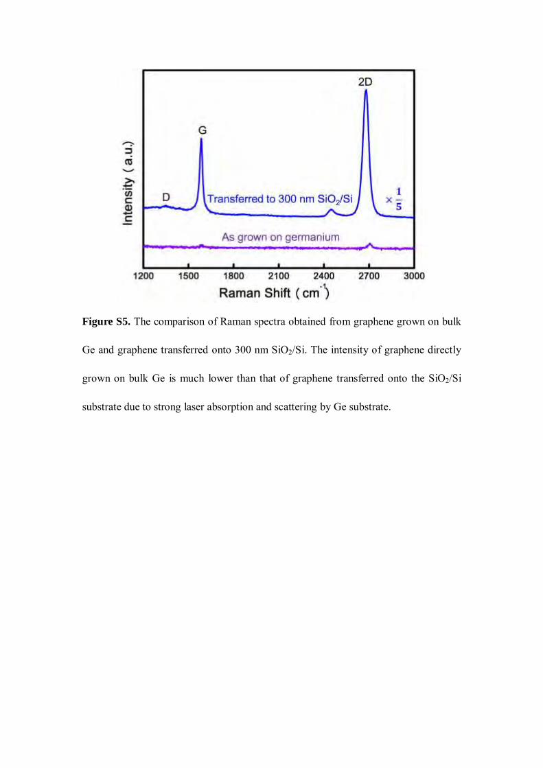
Figure S5. The comparison of Raman spectra obtained from graphene grown on bulk
Ge and graphene transferred onto 300 nm SiO2/Si. The intensity of graphene directly
grown on bulk Ge is much lower than that of graphene transferred onto the SiO2/Si
substrate due to strong laser absorption and scattering by Ge substrate.

Figure S6. a1-e1), OM images of graphene grown on SiO2/Si at 920 oC with different
growth time. Scale bar: 20 μm. a2-e2), Raman mappings of the 2D peak of graphene
from the selected areas marked by yellow dashed squares in a1-e1). Scale bar: 10 μm.
Due to the strong absorption and scattering of excitation laser by the residual Ge, the
scanning Raman image of the 2D band of graphene is closely related to the amount of
residual Ge and thus makes a direct revelation of the distribution of graphene
overlayer very difficult.

Figure S7 a) Raman spectra obtained from graphene grown on Ge coated SiO2/Si for
300 and 360 minutes. b) Raman I2D/IG-mapping of graphene grown on Ge coated
SiO2/Si for 300 minutes. c) Raman I2D/IG-mapping of graphene grown on Ge coated
SiO2/Si for 360 minutes.

Figure S8. (a) SEM image of the fabricated GFET device. (b) Output characteristics
(IDS-VDS) curves of graphene transistor at different VG. The linear IDS-VDS curves
indicate good ohmic contact between the Ti/Au electrodes and graphene channel.

Figure S9. Real-time defogging snapshots taken from the defogging video.

Figure S10. Schematic diagram of the graphene transfer process for TEM
examination.