gecko3 - new generation of the microlab hw/sw co-design
TRANSCRIPT
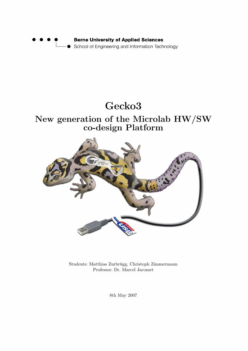
Gecko3New generation of the Microlab HW/SW
co-design Platform
Students: Matthias Zurbrugg, Christoph ZimmermannProfessor: Dr. Marcel Jacomet
8th May 2007


Abstract
The goal of this diploma thesis was to develop the required software for the Gecko3 Board.The Gecko is a development system based on an FPGA for system-on-chip, VLSI designsand educational purpose. The Gecko2 was developed in 2001. Meanwhile the requirementshave risen and new ideas indicate that it is time for a new generation. The new generationincludes a wider concept then the old one. It is now a multi-module system with great flex-ibility, containing a new FPGA board, the Gecko3, and a fast ARM based processor boardcalled Colibri. This concept fulfills the requirements for a scalable system from a simpleeducational system, in combination with a robotic module the so called eBot, to high speedsystems for image-processing, telecommunication and signal-processing applications.
The actually planed features for the Gecko3 board include:
• FPGA with 1.5 Mio. gates
• USB 2.0 interface
• Enough RAM and Flash to support Linux
• Ethernet interface
• Small, as size range of a credit card
• Compatible with IP-Cores included in the Xilinx EDK and from Opencores.org
Our work was divided into different parts of software development. One part was theMicrocontroller software for the Cypress EZ-USB FX2 chip is implemented in C to commu-nicate with the FPGA at high datarates, to configure the FPGA direct from the host PC orfrom the on board serial flash memory and to store FPGA configurations and firmware. Wealso designed hardware cores in VHDL to test the communication with the FPGA and showhow the handshaking between the EZ-USB FX2 and the FPGA works. Another part was thedevelopment of the host PC software to access all functions of the Gecko Board. The goalwas to write a multiplattform software which runs on Windows and Linux and enables a fastand intuitive way for users to use the Gecko Board and implement their specific applicationsoftware.The Gecko3 project is not finished yet, but our diploma thesis is an other big step for itsrealisation.
Project Report i

Inhaltsverzeichnis
Abbildungsverzeichnis v
Tabellenverzeichnis vii
1. Uberblick 11.1. Ziele der Gecko Plattform . . . . . . . . . . . . . . . . . . . . . . . . . . . . . 11.2. Der Vorganger: Gecko2 . . . . . . . . . . . . . . . . . . . . . . . . . . . . . . . 11.3. Die neue Generation . . . . . . . . . . . . . . . . . . . . . . . . . . . . . . . . 21.4. Funktionsumfang des Gecko3 Boards . . . . . . . . . . . . . . . . . . . . . . . 3
2. Definition der Diplomarbeit und Projekt Organisation 5
3. Entwicklungsumgebung 63.1. Entwicklungshardware . . . . . . . . . . . . . . . . . . . . . . . . . . . . . . . 63.2. Entwicklungssoftware . . . . . . . . . . . . . . . . . . . . . . . . . . . . . . . . 73.3. Inbetriebnahme . . . . . . . . . . . . . . . . . . . . . . . . . . . . . . . . . . . 7
4. Kommunikation zwischen EZ-USB und FPGA 104.1. Handshake-Protokoll . . . . . . . . . . . . . . . . . . . . . . . . . . . . . . . . 10
5. VHDL 135.1. Kommunikations Loopback . . . . . . . . . . . . . . . . . . . . . . . . . . . . 13
5.1.1. Zweck und Anforderungen . . . . . . . . . . . . . . . . . . . . . . . . . 135.1.2. Realisierung . . . . . . . . . . . . . . . . . . . . . . . . . . . . . . . . . 135.1.3. Testbench und Simulationsergebnis . . . . . . . . . . . . . . . . . . . . 14
6. Firmware 176.1. Programmstruktur . . . . . . . . . . . . . . . . . . . . . . . . . . . . . . . . . 176.2. USB organisation . . . . . . . . . . . . . . . . . . . . . . . . . . . . . . . . . . 186.3. Grundstruktur der Firmware . . . . . . . . . . . . . . . . . . . . . . . . . . . 196.4. FPGA Konfiguration . . . . . . . . . . . . . . . . . . . . . . . . . . . . . . . . 216.5. Stand-alone Betrieb . . . . . . . . . . . . . . . . . . . . . . . . . . . . . . . . 23
6.5.1. EEPROM beschreiben . . . . . . . . . . . . . . . . . . . . . . . . . . . 236.5.2. EEPROM auslesen . . . . . . . . . . . . . . . . . . . . . . . . . . . . . 25
6.6. FPGA Autokonfiguration . . . . . . . . . . . . . . . . . . . . . . . . . . . . . 266.6.1. SPI Flash beschreiben . . . . . . . . . . . . . . . . . . . . . . . . . . . 266.6.2. SPI Flash auslesen . . . . . . . . . . . . . . . . . . . . . . . . . . . . . 286.6.3. FPGA Bootload . . . . . . . . . . . . . . . . . . . . . . . . . . . . . . 28
6.7. Kommunikation zwischen Host und FPGA . . . . . . . . . . . . . . . . . . . . 296.7.1. Read Waveform . . . . . . . . . . . . . . . . . . . . . . . . . . . . . . . 30
ii Matthias Zurbrugg, Christoph Zimmermann
Inhaltsverzeichnis
6.7.2. Write Waveform . . . . . . . . . . . . . . . . . . . . . . . . . . . . . . 316.7.3. Datenrate . . . . . . . . . . . . . . . . . . . . . . . . . . . . . . . . . . 34
6.8. Vendor Requests . . . . . . . . . . . . . . . . . . . . . . . . . . . . . . . . . . 36
7. Hostsoftware 377.1. Planung . . . . . . . . . . . . . . . . . . . . . . . . . . . . . . . . . . . . . . . 377.2. Realisierung . . . . . . . . . . . . . . . . . . . . . . . . . . . . . . . . . . . . . 387.3. Gecko Library . . . . . . . . . . . . . . . . . . . . . . . . . . . . . . . . . . . . 397.4. Gecko Administrator . . . . . . . . . . . . . . . . . . . . . . . . . . . . . . . . 417.5. Beispielprogramm: Simplecom . . . . . . . . . . . . . . . . . . . . . . . . . . . 42
8. Ausblick 438.1. Weiteres Vorgehen . . . . . . . . . . . . . . . . . . . . . . . . . . . . . . . . . 43
8.1.1. Firmware . . . . . . . . . . . . . . . . . . . . . . . . . . . . . . . . . . 438.1.2. Hostsoftware . . . . . . . . . . . . . . . . . . . . . . . . . . . . . . . . 438.1.3. FPGA Cores . . . . . . . . . . . . . . . . . . . . . . . . . . . . . . . . 438.1.4. Gecko3 Hardware . . . . . . . . . . . . . . . . . . . . . . . . . . . . . . 44
9. Schlusskapitel 45
A. Projekt- und Zeitplanung 47
B. Definition der Verbindung des Spartan3 Boards mit dem EZ-USB FX2Board 51
C. Hex to Bix 53
D. GPIF Designer 55
E. Quellcode 57E.1. Firmware . . . . . . . . . . . . . . . . . . . . . . . . . . . . . . . . . . . . . . 58
E.1.1. Cypress Firmware Framwork . . . . . . . . . . . . . . . . . . . . . . . 58E.1.2. Firmware . . . . . . . . . . . . . . . . . . . . . . . . . . . . . . . . . . 63E.1.3. FPGA Konfiguration . . . . . . . . . . . . . . . . . . . . . . . . . . . . 72E.1.4. EEPROM schreiben und lesen . . . . . . . . . . . . . . . . . . . . . . 74E.1.5. SPI Flash schreiben und lesen . . . . . . . . . . . . . . . . . . . . . . . 77E.1.6. SPI Flash Ansteuerung . . . . . . . . . . . . . . . . . . . . . . . . . . 81E.1.7. SPI Kommunikation . . . . . . . . . . . . . . . . . . . . . . . . . . . . 83E.1.8. Kommunikation zwischen Host und FPGA . . . . . . . . . . . . . . . 85E.1.9. GPIF Waveform Source Code . . . . . . . . . . . . . . . . . . . . . . . 87E.1.10. Headers . . . . . . . . . . . . . . . . . . . . . . . . . . . . . . . . . . . 92
E.2. Loopback Core . . . . . . . . . . . . . . . . . . . . . . . . . . . . . . . . . . . 95E.2.1. Top . . . . . . . . . . . . . . . . . . . . . . . . . . . . . . . . . . . . . 95E.2.2. Datenpfad . . . . . . . . . . . . . . . . . . . . . . . . . . . . . . . . . . 97E.2.3. Statemachine . . . . . . . . . . . . . . . . . . . . . . . . . . . . . . . . 99
E.3. Hostsoftware . . . . . . . . . . . . . . . . . . . . . . . . . . . . . . . . . . . . 103E.3.1. Klasse QGecko . . . . . . . . . . . . . . . . . . . . . . . . . . . . . . . 103E.3.2. Gecko Administrator . . . . . . . . . . . . . . . . . . . . . . . . . . . . 109
Project Report iii
Inhaltsverzeichnis
E.3.3. Simplecom . . . . . . . . . . . . . . . . . . . . . . . . . . . . . . . . . 117
F. Schemas 122F.1. Gecko 3, Stand 9. Dezember 2006 . . . . . . . . . . . . . . . . . . . . . . . . . 122F.2. Flashboard . . . . . . . . . . . . . . . . . . . . . . . . . . . . . . . . . . . . . 141
G. Grossenplanung der Gecko3 Leiterplatte 142
Literaturverzeichnis 143
iv Matthias Zurbrugg, Christoph Zimmermann

Abbildungsverzeichnis
1.1. Aufbau des geplanten eBots (Vollausbau) . . . . . . . . . . . . . . . . . . . . 21.2. Blockdiagramm des Gecko3 Moduls . . . . . . . . . . . . . . . . . . . . . . . . 3
3.1. Abdeckung unserer Entwicklungshardware im Vergleich zum Gecko3 . . . . . 73.2. Xilinx Spartan 3 Starter Kit . . . . . . . . . . . . . . . . . . . . . . . . . . . . 83.3. Cypress EZ-USB FX2LP Development Kit . . . . . . . . . . . . . . . . . . . . 8
4.1. Handshake Blockdiagramm . . . . . . . . . . . . . . . . . . . . . . . . . . . . 104.2. Flussdiagramm vom EZ-USB Richtung FPGA . . . . . . . . . . . . . . . . . . 114.3. Flussdiagramm vom FPGA Richtung EZ-USB . . . . . . . . . . . . . . . . . . 11
5.1. Schema der hochsten Ebene des Loopback Cores . . . . . . . . . . . . . . . . 145.2. Statemachine des Loopback Cores . . . . . . . . . . . . . . . . . . . . . . . . 155.3. Signalverlauf der Simulation des Loopback Cores . . . . . . . . . . . . . . . . 15
6.1. Organisation der Endpoints . . . . . . . . . . . . . . . . . . . . . . . . . . . . 196.2. Grundstruktur der Firmware . . . . . . . . . . . . . . . . . . . . . . . . . . . 206.3. FPGA Konfiguration uber Host . . . . . . . . . . . . . . . . . . . . . . . . . . 226.4. EEPROM beschreiben . . . . . . . . . . . . . . . . . . . . . . . . . . . . . . . 246.5. EEPROM auslesen . . . . . . . . . . . . . . . . . . . . . . . . . . . . . . . . . 256.6. SPI Flash beschreiben . . . . . . . . . . . . . . . . . . . . . . . . . . . . . . . 276.7. SPI Flash auslesen . . . . . . . . . . . . . . . . . . . . . . . . . . . . . . . . . 286.8. GPIF . . . . . . . . . . . . . . . . . . . . . . . . . . . . . . . . . . . . . . . . 296.9. GPIF Read Funktion der Firmware . . . . . . . . . . . . . . . . . . . . . . . . 306.10. Read Waveform (FPGA to GPIF) . . . . . . . . . . . . . . . . . . . . . . . . 316.11. Write Waveform (GPIF to FPGA) . . . . . . . . . . . . . . . . . . . . . . . . 326.12. GPIF Write Funktion der Firmware . . . . . . . . . . . . . . . . . . . . . . . 336.13. Downstream von 512 Byte . . . . . . . . . . . . . . . . . . . . . . . . . . . . . 346.14. Upstream von 512Byte . . . . . . . . . . . . . . . . . . . . . . . . . . . . . . 35
7.1. GUI zur FPGA Konfiguration . . . . . . . . . . . . . . . . . . . . . . . . . . . 417.2. GUI zum Download der Konfigurationsdatei . . . . . . . . . . . . . . . . . . . 417.3. GUI zum Aktualisieren der Firmware . . . . . . . . . . . . . . . . . . . . . . . 417.4. Informationsseite des Gecko Administrators . . . . . . . . . . . . . . . . . . . 41
A.1. Abhanigkeiten der Projektziele . . . . . . . . . . . . . . . . . . . . . . . . . . 48A.2. Soll Zeitplan . . . . . . . . . . . . . . . . . . . . . . . . . . . . . . . . . . . . 49A.3. Ist Zeitplan . . . . . . . . . . . . . . . . . . . . . . . . . . . . . . . . . . . . . 50
C.1. Starten einer zusatzlichen Software nach der Kompilation . . . . . . . . . . . 53
Project Report v

ABBILDUNGSVERZEICHNIS
D.1. Block Diagram Register im GPIF Designer . . . . . . . . . . . . . . . . . . . 55D.2. Waveform der Ubertragungsart zuweisen . . . . . . . . . . . . . . . . . . . . . 56
F.1. Blockdiagramm . . . . . . . . . . . . . . . . . . . . . . . . . . . . . . . . . . . 123F.2. FPGA Blockdiagramm . . . . . . . . . . . . . . . . . . . . . . . . . . . . . . . 124F.3. Erster Teil des FPGAs . . . . . . . . . . . . . . . . . . . . . . . . . . . . . . . 125F.4. Zweiter Teil des FPGAs . . . . . . . . . . . . . . . . . . . . . . . . . . . . . . 126F.5. FPGA Konfiguration und Spannungsversorgung . . . . . . . . . . . . . . . . . 127F.6. DDR SDRAM . . . . . . . . . . . . . . . . . . . . . . . . . . . . . . . . . . . 128F.7. paralleles NOR Flash . . . . . . . . . . . . . . . . . . . . . . . . . . . . . . . . 129F.8. USB 2.0 und FPGA Boot System . . . . . . . . . . . . . . . . . . . . . . . . . 130F.9. I2C Bus mit EEPROM und I/O Baustein . . . . . . . . . . . . . . . . . . . . 131F.10.Ethernet PHY . . . . . . . . . . . . . . . . . . . . . . . . . . . . . . . . . . . 132F.11.SPI Flash, Speicher fur FPGA Konfigurationen . . . . . . . . . . . . . . . . . 133F.12.Schalter, Taster und LEDs . . . . . . . . . . . . . . . . . . . . . . . . . . . . . 134F.13.Erweiterungsbus, 1. Teil . . . . . . . . . . . . . . . . . . . . . . . . . . . . . . 135F.14.Erweiterungsbus, 2. Teil . . . . . . . . . . . . . . . . . . . . . . . . . . . . . . 136F.15.Spannungsversorgung . . . . . . . . . . . . . . . . . . . . . . . . . . . . . . . 137F.16.JTAG Anschluss . . . . . . . . . . . . . . . . . . . . . . . . . . . . . . . . . . 138F.17.Ethernet Anschluss Print . . . . . . . . . . . . . . . . . . . . . . . . . . . . . 139F.18.RS232 Anschluss Print . . . . . . . . . . . . . . . . . . . . . . . . . . . . . . . 140F.19.Adapterprint Intel NOR Flash . . . . . . . . . . . . . . . . . . . . . . . . . . 141
G.1. Zeichnung des Gecko3 Board im Masssstab 1:1 . . . . . . . . . . . . . . . . . 142
vi Matthias Zurbrugg, Christoph Zimmermann

Tabellenverzeichnis
B.1. Definition der Verbindung zwischen dem Spartan 3 Starter Kit und dem EZ-USB FX2LP Development Kit . . . . . . . . . . . . . . . . . . . . . . . . . . 52
Project Report vii


1. Uberblick
Dieses Kapitel dient dazu, dem Leser einen Uberblick uber das ganze Projekt und der Vor-geschichte zu geben.
1.1. Ziele der Gecko Plattform
Wie der Titel dieser Arbeit andeutet, handelt es sich bei diesem Projekt nicht um eine Neu-entwicklung, sondern um die konsequente Weiterfuhrung des bestehenden Gecko Konzepts.Dieses Konzept beinhaltet eine universell einsetzbare Hardware Plattform, hauptsachlich be-stehend aus einem FPGA, die es ermoglicht in kurzer Zeit Projekte aus dem Gebiet VLSIoder SoC (System on Chip) zu realisieren und zu testen. Sie dient auch als Ubungsplattformin den Fachern Digitaltechnik und VLSI Design, die es den Studenten erlaubt die Theoriepraktisch zu vertiefen. Zu diesem Zweck existiert auch ein einfaches Robotermodell genannteducational Robot (Kurz eBot).
Bei Semester- und Diplomarbeiten erlaubt das Gecko Konzept, dass sich die Studentenauf die eigenen Projektziele konzentrieren konnen, da die komplexesten Komponenten schonauf dem Gecko Modul vorhanden sind und nicht jedesmal eine komplette Neuentwicklunggemacht werden muss. So mussen nur noch die applikationsspezifischen Komponenten, wieSensoren, Aktoren, Kommunikationsinterfaces, Leistungsstufen etc. hinzugefugt werden.
1.2. Der Vorganger: Gecko2
Gecko2 folgte kurz nach der Entwicklung des ersten Gecko Moduls und unterscheidet sichdavon hauptsachlich durch die zusatzliche USB 1.1 Schnittstelle, uber die es moglich ist denFPGA zu konfigurieren und Daten mit dem PC auszutauschen. Das Modul wurde im Jahr2001 entwickelt.
Das Gecko2 Modul bietet:
• Xilinx Spartan2 FPGA mit 200 kGatter
• Xilinx Platform Flash zur FPGA Konfiguration
• Cypress EZ-USB Chip fur die Kommunikation per USB 1.1
• Zwei 64 K x 16 Bit SRAM
• Sechs LEDs und ein Taster zur freien Nutzung
• Zwei 64 Pin Stecker an denen Erweiterungen angeschlossen werden konnen
• Kompakte Abmessungen (86x86mm)
Project Report 1
1. Uberblick
Die Moglichkeiten dieser Plattform sind vielfaltig. Es steht ein Microchip PIC16C5X oderPIC16C7X kompatibler Mikrocontroller als IP-Core zur Verfugung. Das ganze System kannuber die USB Schnittstelle programmiert werden und es konnen Daten mit dem Host PC aus-getauscht werden. Eine Anbindung an Matlab bzw. Simulink steht fur den Gecko2 ebenfallszur Verfugung.
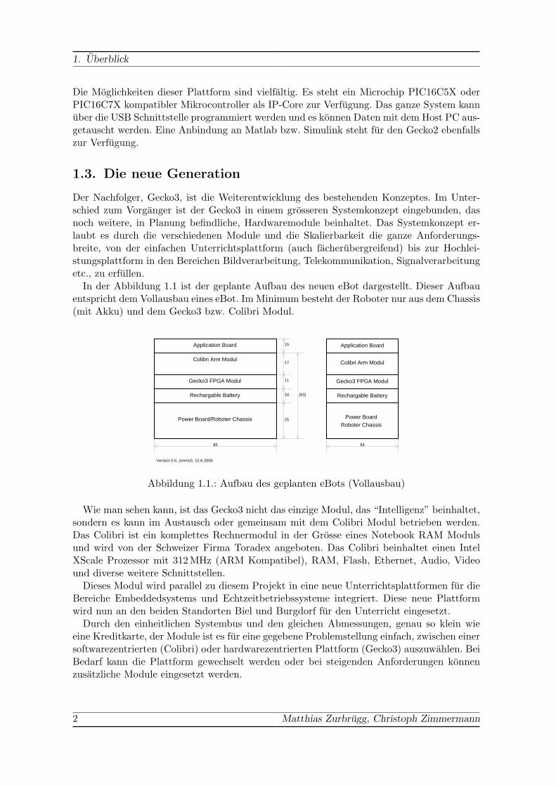
1.3. Die neue Generation
Der Nachfolger, Gecko3, ist die Weiterentwicklung des bestehenden Konzeptes. Im Unter-schied zum Vorganger ist der Gecko3 in einem grosseren Systemkonzept eingebunden, dasnoch weitere, in Planung befindliche, Hardwaremodule beinhaltet. Das Systemkonzept er-laubt es durch die verschiedenen Module und die Skalierbarkeit die ganze Anforderungs-breite, von der einfachen Unterrichtsplattform (auch facherubergreifend) bis zur Hochlei-stungsplattform in den Bereichen Bildverarbeitung, Telekommunikation, Signalverarbeitungetc., zu erfullen.
In der Abbildung 1.1 ist der geplante Aufbau des neuen eBot dargestellt. Dieser Aufbauentspricht dem Vollausbau eines eBot. Im Minimum besteht der Roboter nur aus dem Chassis(mit Akku) und dem Gecko3 bzw. Colibri Modul.
Application Board
Colibri Arm Modul
Gecko3 FPGA Modul
Rechargable Battery
Power Board/Roboter Chassis 25
11
10
15
17
(63)
Version 0.5, zimmc5, 15.6.2006
85
Application Board
Colibri Arm Modul
Gecko3 FPGA Modul
Rechargable Battery
Power BoardRoboter Chassis
54
Abbildung 1.1.: Aufbau des geplanten eBots (Vollausbau)
Wie man sehen kann, ist das Gecko3 nicht das einzige Modul, das “Intelligenz” beinhaltet,sondern es kann im Austausch oder gemeinsam mit dem Colibri Modul betrieben werden.Das Colibri ist ein komplettes Rechnermodul in der Grosse eines Notebook RAM Modulsund wird von der Schweizer Firma Toradex angeboten. Das Colibri beinhaltet einen IntelXScale Prozessor mit 312 MHz (ARM Kompatibel), RAM, Flash, Ethernet, Audio, Videound diverse weitere Schnittstellen.
Dieses Modul wird parallel zu diesem Projekt in eine neue Unterrichtsplattformen fur dieBereiche Embeddedsystems und Echtzeitbetriebssysteme integriert. Diese neue Plattformwird nun an den beiden Standorten Biel und Burgdorf fur den Unterricht eingesetzt.
Durch den einheitlichen Systembus und den gleichen Abmessungen, genau so klein wieeine Kreditkarte, der Module ist es fur eine gegebene Problemstellung einfach, zwischen einersoftwarezentrierten (Colibri) oder hardwarezentrierten Plattform (Gecko3) auszuwahlen. BeiBedarf kann die Plattform gewechselt werden oder bei steigenden Anforderungen konnenzusatzliche Module eingesetzt werden.
2 Matthias Zurbrugg, Christoph Zimmermann
1.4. Funktionsumfang des Gecko3 Boards
Das Konzept einer einheitlichen Hardwareplattform kann bei Bedarf noch erweitert werdenz. B. mit einem DSP Modul, das es erlauben wurde, Algorithmen in Software oder Hardwarezu implementieren und in der gleichen Applikation auszutesten.
Das Roboterchassis fur die neue Generation befindet sich auch in Entwicklung und sollden bestehenden eBot ersetzen.
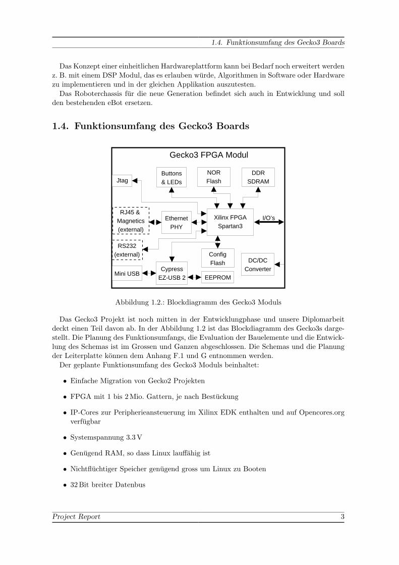
1.4. Funktionsumfang des Gecko3 Boards
Gecko3 FPGA Modul
I/O’s
RS232(external) Config
Flash DC/DCConverter
EEPROMCypress
EZ-USB 2Mini USB
Xilinx FPGASpartan3
JtagNORFlash
DDRSDRAM
EthernetPHY
RJ45 & Magnetics(external)
Buttons& LEDs
Abbildung 1.2.: Blockdiagramm des Gecko3 Moduls
Das Gecko3 Projekt ist noch mitten in der Entwicklungphase und unsere Diplomarbeitdeckt einen Teil davon ab. In der Abbildung 1.2 ist das Blockdiagramm des Gecko3s darge-stellt. Die Planung des Funktionsumfangs, die Evaluation der Bauelemente und die Entwick-lung des Schemas ist im Grossen und Ganzen abgeschlossen. Die Schemas und die Planungder Leiterplatte konnen dem Anhang F.1 und G entnommen werden.
Der geplante Funktionsumfang des Gecko3 Moduls beinhaltet:
• Einfache Migration von Gecko2 Projekten
• FPGA mit 1 bis 2 Mio. Gattern, je nach Bestuckung
• IP-Cores zur Peripherieansteuerung im Xilinx EDK enthalten und auf Opencores.orgverfugbar
• Systemspannung 3.3 V
• Genugend RAM, so dass Linux lauffahig ist
• Nichtfluchtiger Speicher genugend gross um Linux zu Booten
• 32 Bit breiter Datenbus
Project Report 3

1. Uberblick
• USB 2.0 anstatt USB 1.1 Schnittstelle
• RS232 Schnittstelle
• Ethernet Schnittstelle
• Schnittstelle mit hoher Bandbreite zwischen Colibri und Gecko3 bzw. zwischen zweiGecko3s
• Abmessungen so klein wie eine Visitenkarte (54 x 85 mm)
• geringe Hohe (ca. 10mm)
4 Matthias Zurbrugg, Christoph Zimmermann
2. Definition der Diplomarbeit undProjekt Organisation
Unsere Diplomarbeit deckt einen Teil der Entwickung der nachsten Gecko Generation ab.Unsere Aufgabe war es, die fur dieses Board notwendige Software zu Programmieren. ImDetail umfasst dies die folgenden Teilziele:
• USB Kommunikation Host PC mit dem Cypress EZ-USB
• Konfiguration des FPGAs
• Kommunikation mit dem FPGA, mit Fokus auf hohe Ubertragunsgeschwindigkeit.
• Ansteuerung des SPI Flash Speichers
• Ansteuerung des I2C EEPROMs
• Ansteuerung des NOR Flash Speichers
• Definition des USB Protokolls zwischen Host und Gecko3
• Realisierung des stand-alone Betriebs ohne Host PC
• Programmieren der Host PC Software und Beispielen fur den Anwender
• Test und Prufung des Schemas der abgedeckten Teilsysteme
• Betreuung des Layoutvorgangs der Gecko3 Leiterplatte
Zu Beginn der Diplomarbeit war das Projekt soweit Forgeschritten, dass die gesammteEvaluation, die Definition des Funktionsumfangs, die Schaltungsentwicklung und die mecha-nische Vorplanung abgeschlossen waren.
Am Anfang unserer Diplomarbeit planten wir den ganzen Ablauf und die Arbeitsteilungunseres Projekts. Dazu erstellten wir zuerst eine Tabelle, die die Abhangigkeiten der Projekt-ziele aufzeigte. Aufgrund dieser Tabelle entwarfen wir einen Zeitplan fur unsere Diplomarbeitaus dem auch die Arbeitsaufteilung ersichtlich war. Die Dokumente der Projektplanung sindim Anhang A zu finden.
Project Report 5

3. Entwicklungsumgebung
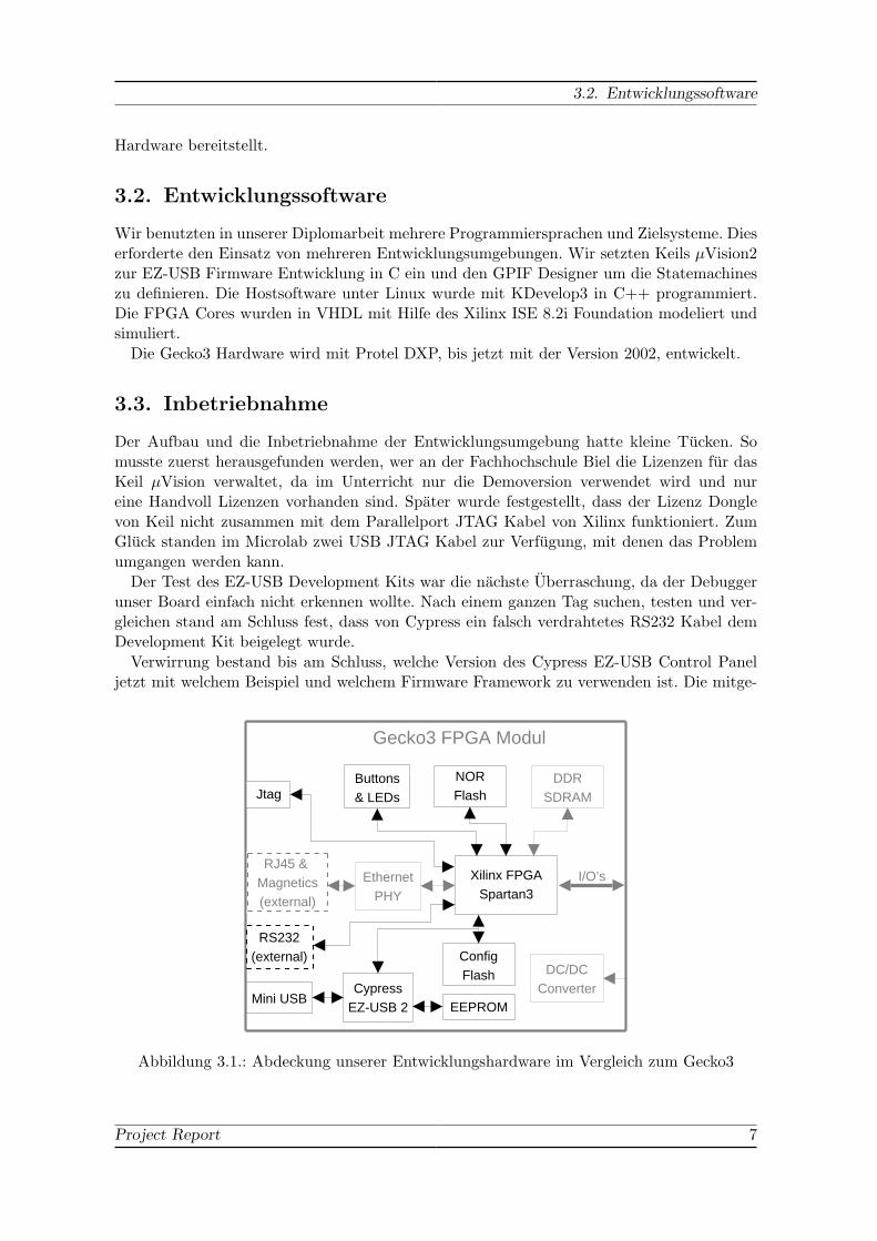
3.1. Entwicklungshardware
Die Hardware Entwicklung des Gecko3 ist noch nicht abgeschlossen und es wurde auch nochkein Prototyp realisiert. Somit stand auch fur unsere Diplomarbeit kein richtiges Zielsystemzum Programmieren zur Verfugung. Dazu kommt, dass die EZ-USB FX2 Chip Variante aufdem Gecko3 so weit in der Funktionalitat eingeschrankt ist, dass keine Moglichkeit mehrbesteht die Software in einem Debugger laufen zu lassen.
Unsere erste Aufgabe bestand also darin, eine Entwicklungshardware zusammen zu stellendie moglichst aquivalent zum geplanten Gecko3 ist. Zur Verfugung standen uns zwei Spartan3 Starter Kits von Xilinx, die jeweils mit einem 200 kGatter FPGA bestuckt sind, und einEZ-USB FX2LP Development Kit von Cypress. Das EZ-USB FX2 Board und ein XilinxBoard bildeten die Basis fur unsere Zielhardware.
Diesen beiden Boards fehlen aber wesentliche Komponenten des Gecko3, welche uber zweizusatzliche Leiterplatten hinzugefugt werden. Die erste beherbergt das SPI Flash von ST undden I2C I/O-Chip von NXP. Diese wird an das EZ-USB Development Board angeschlossen.Die zweite Leiterplatte beherbergt zwei Intel NOR Flash Chips und wird an zwei Erweite-rungsstecker des Spartan 3 Starter Kits angeschlossen (Schema im Anhang F.2), uber dendritten Erweiterungsstecker wird der Spartan 3 FPGA mit dem EZ-USB verbunden.
Die Verkabelung der zwei Board untereinander ist in der Tabelle B.1 aufgelistet. Ursprung-lich war vorgesehen, dass in beiden Modi, Konfiguration wie Kommunikation, die Datenlei-tungen die selbe Nummer tragen um einheitlich zu bleiben. Wie den Xilinx Dokumenten([NP02] und [Tse04]) zu entnehmen ist, muss bei der Konfiguration jedes Byte im Bitstromin seiner Reihenfolge umgedreht werden (Das MSB muss an den FPGA Anschluss D0 unddas LSB an D7). Da diese Operation mit Software sehr ineffizient zu losen ist und die FPGADatenleitungen nach der Konfiguration frei belegbar sind, haben wir uns entschieden, einfachdie Verbindungen umzudrehen, D0 vom EZ-USB ist so mit D7 des FPGAs verbunden. DerAnwender merkt im Kommunikationsmodus nichts davon solange er sich an die Pinbelegungin der Tabelle halt. Um uns etwas Verdrahtungsarbeit zu ersparen und der ganze Aufbau et-was ubersichtlicher zu machen, haben wir uns entschieden den Kommunikationsmodus auchnur auf dieser 8 Bit Busbreite zu betreiben (6.7.3).
Das EZ-USB Development Kit wird normalerweise uber die USB Schnittstelle versorgt.Damit ein stand-alone Betrieb realisiert werden konnte, musste die Stromversorgung derbeiden Boards verbunden werden. Das Netzteil des Spartan 3 Starter Kits versorgt nun dieganze Entwicklungshardware. Um Storungen zu reduzieren wurden zwei Drosselspulen in dieVersorgungsleitungen zum EZ-USB Board eingebaut.
Zur Uberprufung und Fehlersuche stand uns ein Logic Analyser HP 16500B (80 Kanale,100 MHz) und ein Speicheroszilloskop Tektronix TDS 754C (4 Kanal, 2 GSamples/s) zur Ver-fugung.
Unsere Entwicklungshardware deckt nicht den vollstandigen Funktionsumfang des Gecko3Boards ab. In der Graphik 3.1 sind die Funktionsblocke dunkel hervorgehoben welche unsere
6 Christoph Zimmermann
3.2. Entwicklungssoftware
Hardware bereitstellt.
3.2. Entwicklungssoftware
Wir benutzten in unserer Diplomarbeit mehrere Programmiersprachen und Zielsysteme. Dieserforderte den Einsatz von mehreren Entwicklungsumgebungen. Wir setzten Keils µVision2zur EZ-USB Firmware Entwicklung in C ein und den GPIF Designer um die Statemachineszu definieren. Die Hostsoftware unter Linux wurde mit KDevelop3 in C++ programmiert.Die FPGA Cores wurden in VHDL mit Hilfe des Xilinx ISE 8.2i Foundation modeliert undsimuliert.
Die Gecko3 Hardware wird mit Protel DXP, bis jetzt mit der Version 2002, entwickelt.
3.3. Inbetriebnahme
Der Aufbau und die Inbetriebnahme der Entwicklungsumgebung hatte kleine Tucken. Somusste zuerst herausgefunden werden, wer an der Fachhochschule Biel die Lizenzen fur dasKeil µVision verwaltet, da im Unterricht nur die Demoversion verwendet wird und nureine Handvoll Lizenzen vorhanden sind. Spater wurde festgestellt, dass der Lizenz Donglevon Keil nicht zusammen mit dem Parallelport JTAG Kabel von Xilinx funktioniert. ZumGluck standen im Microlab zwei USB JTAG Kabel zur Verfugung, mit denen das Problemumgangen werden kann.
Der Test des EZ-USB Development Kits war die nachste Uberraschung, da der Debuggerunser Board einfach nicht erkennen wollte. Nach einem ganzen Tag suchen, testen und ver-gleichen stand am Schluss fest, dass von Cypress ein falsch verdrahtetes RS232 Kabel demDevelopment Kit beigelegt wurde.
Verwirrung bestand bis am Schluss, welche Version des Cypress EZ-USB Control Paneljetzt mit welchem Beispiel und welchem Firmware Framework zu verwenden ist. Die mitge-
Gecko3 FPGA Modul
I/O’s
RS232(external) Config
Flash DC/DCConverter
EEPROMCypress
EZ-USB 2Mini USB
Xilinx FPGASpartan3
NORFlash
DDRSDRAM
EthernetPHY
RJ45 & Magnetics(external)
Buttons& LEDsJtag
Abbildung 3.1.: Abdeckung unserer Entwicklungshardware im Vergleich zum Gecko3
Project Report 7

3. Entwicklungsumgebung
Abbildung 3.2.: Xilinx Spartan 3 Starter KitAbbildung 3.3.: Cypress EZ-USB FX2LP De-
velopment Kit
8 Christoph Zimmermann

3.3. Inbetriebnahme
lieferten Beispiele auf der EZ-USB FX2LP Development Kit CD funktionieren nur mit derVorgangerversion die wir auf der CD des Xcelerator Development Kits gefunden haben. DieInformationen von Cypress zu diesem Thema fehlen komplett. Wir empfehlen weiterhin dasalte Control Panel zu verwenden, da die Beispiele der EZ-USB FX2LP CD nur damit ver-wendet werden konnen und auch Cypress gemass den Screenshots in ihren Dokumentationennoch mit dieser Version arbeitet.
Der I2C I/O-Chip konnte nicht benutzt werden, da von NXP falsche Muster geliefertwurden. Dies wurde leider erst bemerkt als der Chip benutzt werden sollte. So war es wahrendder Diplomarbeit leider nicht mehr moglich einen richtigen Chip zu bekommen.
Project Report 9

4. Kommunikation zwischen EZ-USB undFPGA
Bei der Kommunikation mit dem FPGA geht es darum, dem Benutzer eine transparenteVerbindung zwischen Host und dem Spartan 3 uber die USB 2.0 Schnittstelle zur Verfugungzu stellen. Dafur wurde ein eigenes Handshake-Protokoll zwischen dem EZ-USB FX2 unddem FPGA definiert. Mit dem EZ-USB FX2 ist dabei nur das General Purpose Interface(GPIF) gemeint, das vom Handshaking betroffen ist und im Unterkaptiel 6.7 erklart wird.Die Abbildung 4.1 illustriert das Blockdiagramm des Handshaking.
Abbildung 4.1.: Handshake Blockdiagramm
4.1. Handshake-Protokoll
Unser Handshake-Protokoll basiert auf dem Prinzip des vier Phasen Handshaking [Jac]. Nurist in unserem Fall kein fester Master und Slave definiert. Somit muss zuerst kontrolliertwerden ob der Bus frei ist. Dann sendet der Initiator, also der momentane Master, einenRequest und erwartet die Bestatigung vom temporaren Slave. Erst nach diesem Bus-Handlingwerden die Daten vom Sender an den Bus gelegt.
Der Slave empfangt die Daten und bestatigt seinen abgeschlossenen Lesevorgang, indemer seine Bestatigung wieder loscht. Wenn noch weitere Daten zu senden sind wird die gan-ze Prozedur wiederholt bis die Informationen vollstandig ubertragen sind. Das Ende einerUbertragung wird mit einer Regelverletzung angezeigt. Der Initator setzt sein Ready-Flagund verstosst somit gegen die Regeln des Handshake-Protokolls. Der Slave erkennt somit dasEnde einer Ubertragung und setzt ebenfalls sein Ready-Flag. Nachdem zuerst der Masterund dann der Slave ihre Bestatigungen loschen, kehrt das GPIF in den Idle State zuruck.Die Abbildung 4.2 zeigt das Handshaking einer Datenubertragung vom EZ-USB FX2 zumFPGA.
10 Matthias Zurbrugg

4.1. Handshake-Protokoll
Abbildung 4.2.: Flussdiagramm vom EZ-USB Richtung FPGA
Um die bidirektionale Datenubertragung zu vervollstandigen, ist in Abbildung 4.3 nocheine Datenubertragung vom FPGA zum EZ-USB dargestellt. Das Handshaking kummert sich
Abbildung 4.3.: Flussdiagramm vom FPGA Richtung EZ-USB
nicht um die Lange der ubertragenen Daten. Wenn vom Host die Daten gesendet werden, istdas kein Problem da unser Protokoll, solange sendet bis der FIFO Buffer nicht mehr gefulltwird. In der entgegengesetzten Richtung ist das jedoch problematisch, da beim Bulk-TransferVerfahren (siehe Kapitel 6.2) der Host dem EZ-USB FX2 mitteilen muss wieviele Byte er
Project Report 11
4. Kommunikation zwischen EZ-USB und FPGA
lesen will. Momentan kommunizieren wir noch uber einen Loopback Core im FPGA (sieheKapitel 5.1), das heisst die Datenmenge, die gesendet wird, kommt auch wieder zuruck.Somit wissen wir naturlich wieviel der Host lesen will. Bei einer anderen Konfiguration musser aber vor der Ubertragung wissen wieviele Daten der FPGA senden will.
Diese Aufgabe soll spater ein Protokoll eine Ebene uber dem Handshaking ubernehmen.Dieses Protokoll existiert noch nicht, doch erste Uberlegungen haben uns mehrere Moglich-keiten aufgezeigt:
• Die Firmware teilt dem Host vor jedem Transfer den FIFO Fullstand mit einem VendorRequest mit.
• Der FPGA versieht den Datenstrom mit einer Endmarke. Der Host liest dann immerden gesammten Inhalt des FIFO Buffers und sucht nach der Endmarke.
• Es wird eine feste Lange der Datenpakete definiert. Der FPGA wurde dann nichtgefullte Datenpakete mit Dummy-Informationen erganzen.
Die zwei letzten Moglichkeiten sind ahnlich, wobei die dritte Variante einen hoheren Auf-wand fur den FPGA bedeutet. Doch die beste Losung fur dieses Problem zu finden ist Teileiner nachsten Arbeit.
Die Signalisation des Datenendes durch eine Regelverletzung haben wir wegen der fehlen-den RDY-Leitung realisiert. Diese Leitungen sind neben den zwei internen Flags die einzigenInputs die vom GPIF eingelesen werden konnen. Da wir auf dem Gecko3 die kleinste Versiondes EZ-USB FX2 einsetzen, haben wir nur zwei RDY-Leitungen zur Verfugung, welche aberschon von unserem Handshaking genutzt werden. Somit bleiben keine weiteren Eingange,die vom GPIF genutzt werden konnen.
Eine weitere Moglichkeit ware eine Endsignalisation mit Hilfe eines Interrupts zu reali-sieren und das GPIF somit manuell aus der Firmware abzubrechen. Diese Losung erschienuns jedoch als unstrukturiert, weil der Mikrokontroller in den Kommunikationsablauf ein-greifen musste. Diese Unabhangikeit von der Firmware bezahlen wir jedoch mit einem etwasaufwandigerem Handshaking, das am Ende der Ubertragung etwas langer ist und somitdie Datenrate etwas dampft. Je grosser aber die Datenpakete sind, desto seltener werdendie Endsignalisationen. Somit wird auch deren negativer Einfluss auf die Datenrate immerkleiner.
12 Matthias Zurbrugg

5. VHDL
In diesem Kapitel beschreiben wir die Entwicklungen die wir fur den FPGA gemacht haben.Es wurde alles in VHDL im Xilinx ISE programmiert [Sch03]. Auch zur Simulation wurdedas ISE benutzt. Als Synthesewerkzeug kam Xilinx XST zum Einsatz.
Wie aus dem Projektplan ersichtlich ist, waren weitere Cores geplant, konnten aber inder zur Verfugung stehenden Zeit nicht mehr realisiert werden. Darum folgt hier nur dieBeschreibung des Loopback Cores.
5.1. Kommunikations Loopback
5.1.1. Zweck und Anforderungen
Der Loopback Core dient zum Entwickeln und Testen der Kommunikation zwischen demFPGA und dem EZ-USB Chip. Er stellt also eine einfache Implementierung des im Kapitel4 beschriebenen Handshake-Protokolls dar. Die Daten die vom EZ-USB gesendet werden,mussen bis zum Abschluss der Sequenz gespeichert werden und sollen danach zuruckgesendetwerden. Dies ermoglicht eine Uberprufung der gesendeten Daten und beider Kommunika-tionswege. Der Core muss Sequenzen speichern konnen, die langer als ein Wort sind, da inder Anwendung normalerweise grossere Datenmengen ausgetauscht werden sollen und dieUSB Schnittstelle nur bei grosseren Datenblocken die hohen Datenraten erreicht. Die VHDLSourcecodes sind im Anhang ab E.2 zu finden.
5.1.2. Realisierung
Dem Loopback Core liegt ein klassischer FSM-D (Finite-State-Machine/Datapath) Ansatzzu Grunde. Diesem Ansatz folgend wurde zuerst der Datenpfad erstellt. Als zentrales Elementdient ein Block RAM Element. Block RAMs sind direkt als Hardware im Spartan 3 integriertund mussen nicht synthetisiert werden. Der Vorteil dabei ist, dass keine Speicherstrukturerzeugt werden muss. Das spart Zeit bei der Entwicklung und schont die FPGA Ressourcen,da diese ineffizent fur regelmassige Strukturen sind. Der Nachteil daran ist die Abhangigkeitder Zielplattform, da Block RAMs nur in Xilinx FPGAs (Spartan 3 oder Virtex 2 undhoher) vorhanden sind. Der Rest des Datenpfads besteht aus einem Auf-/Abwartszahler alsAdressgenerator, einem Nulldetektor und dem Tri-State Buffer fur den Datenbus.
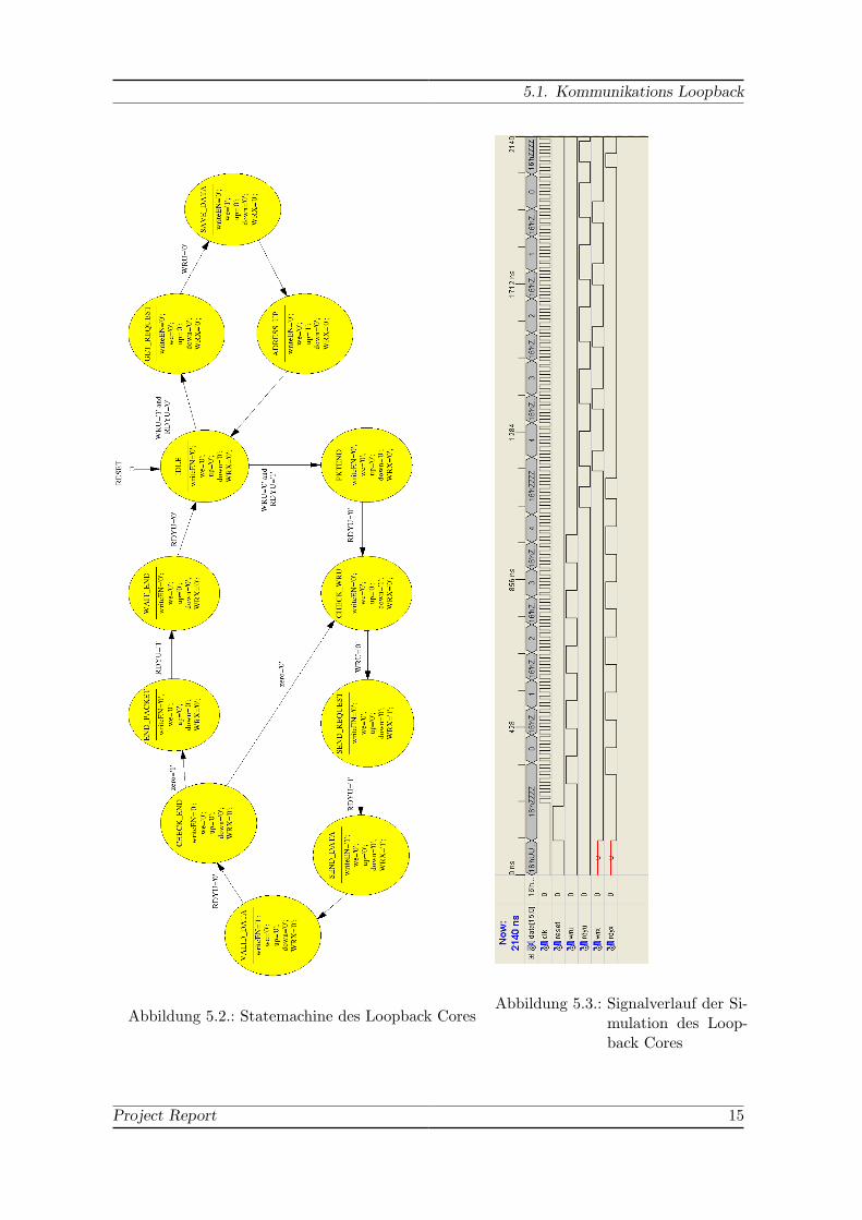
Die Statemachine wurde anschliessend im Xilinx ISE mit Hilfe des Programms StateCADgezeichnet. Dieses erlaubt die graphische Eingabe der Zustande, den Ubergangen, der Si-gnalwerte und den Bedingungen und generiert daraus wahlweise VHDL oder Verilog Code.Dieser Weg wurde zum einen aus Neugier an der graphischen Eingabe gewahlt und zumanderen weil Anderungen einfacher vorgenommen werden konnen. Damit muss die Doku-mentation (State Event Diagramm) nicht separat erstellt werden und ist immer aktuell. Dieso erstellte Statemachine ist in Abbildung 5.2 dargestellt.
Project Report 13

5. VHDL
Die Statemachine ubernimmt die Abhandlung des Handshake-Protokolls mit dem EZ-USBund steuert dementsprechend die Signale des Datenpfads. Durch die sehr einfache Implemen-tierung wird beim Empfangen der Adresszahler hinauf- und beim Senden heruntergezahlt.Dadurch werden die Daten in umgekehrter Reihenfolge zuruckgesendet (LIFO).
Das in Abbildung 5.1 dargestellte Topmodul des Loopback enthalt ein entscheidendesElement, das nach den Tests mit dem EZ-USB hinzugefugt werden musste: Zwei zusatzli-che Buffer, die die Handshake Eingangssignale zwischenspeichern bevor sie zur Statemachinegelangen. Diese sind notig, weil wir bei Messungen festgestellt haben dass wir mit Metastabi-litat zu kampfen haben. Dies wird durch unser asynchrones System ausgelost und kann nichtverhindert werden. Mit Hilfe des Double-Bufferings kann das Risiko Metastabilerzustandemassiv reduziert werden [Cad00]. Dies wurde auch durch unsere Tests bestatigt.
Dieser Core ist nur eine “Testschaltung”, eine Implementierung fur eine Applikation musssicher um zusatzliche Elemente zur Fehlerbehandlung, Prufung des Speicherfullstands undeinem Watchdog erganzt werden.
5.1.3. Testbench und Simulationsergebnis
Fur die Progammierung der Testbench wurde ein anderer Codierstil gewahlt, da Core undTestbench von der gleichen Person erstellt wurden. Dieses Vorgehen reduziert die Wahr-scheinlichkeit, dass sich ein Fehler sowohl in den Core wie auch in die Testbench einschleichtund bis am Schluss unentdeckt bleibt.
Abbildung 5.1.: Schema der hochsten Ebene des Loopback Cores
14 Christoph Zimmermann
5.1. Kommunikations Loopback
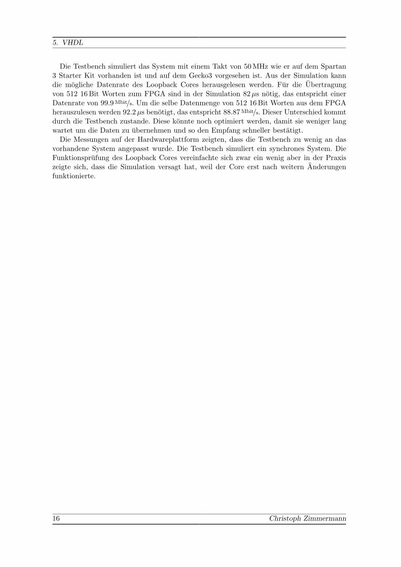
Abbildung 5.2.: Statemachine des Loopback CoresAbbildung 5.3.: Signalverlauf der Si-
mulation des Loop-back Cores
Project Report 15
5. VHDL
Die Testbench simuliert das System mit einem Takt von 50 MHz wie er auf dem Spartan3 Starter Kit vorhanden ist und auf dem Gecko3 vorgesehen ist. Aus der Simulation kanndie mogliche Datenrate des Loopback Cores herausgelesen werden. Fur die Ubertragungvon 512 16 Bit Worten zum FPGA sind in der Simulation 82µs notig, das entspricht einerDatenrate von 99.9 Mbit/s. Um die selbe Datenmenge von 512 16 Bit Worten aus dem FPGAherauszulesen werden 92.2 µs benotigt, das entspricht 88.87 Mbit/s. Dieser Unterschied kommtdurch die Testbench zustande. Diese konnte noch optimiert werden, damit sie weniger langwartet um die Daten zu ubernehmen und so den Empfang schneller bestatigt.
Die Messungen auf der Hardwareplattform zeigten, dass die Testbench zu wenig an dasvorhandene System angepasst wurde. Die Testbench simuliert ein synchrones System. DieFunktionsprufung des Loopback Cores vereinfachte sich zwar ein wenig aber in der Praxiszeigte sich, dass die Simulation versagt hat, weil der Core erst nach weitern Anderungenfunktionierte.
16 Christoph Zimmermann
6. Firmware
Der EZ-USB FX2 hat neben seiner USB Peripherie einen 8051 Mikroprozessor integriert, waseine Implementation der Firmware im C Code ermoglicht. Die Firmware kann direkt vomHost uber USB oder beim Booten vom EEPROM via I2C ins intern RAM geladen werden.Die zweite Variante setzt voraus, dass vor dem Reset des EZ-USB FX2 die Firmware einbootfahiges Abbild von sich im EEPROM abgespeichert hat.
Die erste Version unserer Gecko Firmware kann folgende Grundfunktion ausfuhren:
• FPGA direkt vom Host uber USB konfigurieren
• Bootfahige Firmware vom Host via USB ins EEPROM schreiben
• wahlbare Anzahl Byte aus EEPROM lesen und uber USB an Host senden (zum De-buggen)
• FPGA Konfiguration vom Host uber USB ins SPI Flash schreiben
• feste Anzahl Byte aus SPI Flash lesen und via USB an Host senden (zum Debuggen)
• nach einem Booten aus dem EEPROM automatisch den FPGA aus dem SPI Flashkonfigurieren
• Kommunikation zwischen Host und FPGA
• Ruckgabe der Firmware Version bei der Anfrage des Hosts
6.1. Programmstruktur
Cypress empfiehlt die Firmware in ihrem vorbereiteten µVision2 Projekt zu integrieren,was wir auch gemacht haben. Das Projekt findet man nach der Installation der CypressDevelopment Kit Software im Ordner Target und enthalt folgende Dateien:
• Fw.c ist das Cypress Firmware Framework, welche das USB Handling (Interrupts, Enu-meration, Renumeration etc.) ubernimmt. Darin enthalten ist auch die C-Grundfunktionmain(). Cypress empfiehlt den Code in dieser Datei nicht zu editieren. Alle fur den Pro-grammierer notigen Veranderungen sollen in der Periph.c gemacht werden.
• Periph.c enthalt schon eine Vielzahl von vordefinierten Funktionen. Wir verwenden inunserer Firmware die Initialisierungsfunktion, welche einmal von Fw.c aufgerufen wird,die Funktion TD Poll(), die regelmassig aus dem main() gestartet wird und die defini-tion der Vendor Requests. Den restlichen Code im Periph.c haben wir so belassen wieer von Cypress vorbereitet wurde. Somit konnen spater Anderungen gemacht werden,ohne das ein Einblick in das original µVision2 Projekt notig ist.
• Gpif.c wird vom GPIF Designer erstellt und enthalt die Waveform Descriptor Tables.
Project Report 17
6. Firmware
• Ezusb.lib enthalt eine Sammlung von Funktionen wie das Lesen und Schreiben des I2CBuses etc.
• USBJmpTb.obj beinhaltet die Interrupt Vector Tables fur das USB (INT2) und dasGPIF (INT4).
• Dscr.a51 definiert die gesamten USB Descriptor Tables.
6.2. USB organisation
Der gesamte Datenaustausch lauft bei USB uber sogenannte Endpoints (EP). Diese End-points sind mit einer Ausnahme alle unidirektional und ermoglichen einen voneinander un-abhangigen Datenfluss. Der Endpoint 0 ist fur Steuerfunktionen, sogenannte Vendor Re-quests, reserviert und bidirektional. Die folgende Aufliestung gibt einen Uberblick uber dievon uns verwendeten Endpoints. Um mehr Informationen zum Thema USB zu erhalten,verweisen wir auf die einschlagige Literatur [Hyd99], [Cyp06].
• EP0 wird als IN/OUT Endpoint benutzt und ist fur Vendor Requests reserviert.
• EP2 ist als OUT Endpoint konfiguriert und wird fur alle Datentransfers ausser derKommunikation mit dem FPGA verwendet
• EP4 hat die selbe Aufgabe wie EP2 nur als IN Endpoint in die entgegengesetzte Rich-tung.
• EP6 ist der OUT Endpoint der FPGA Kommunikation und direkt mit dem GPIFverbunden.
• EP8 hat die selbe Aufgabe wie EP6 nur als IN Endpoint in die entgegengesetzte Rich-tung.
EP2 und EP4 sind dabei als Interface 0 und EP6 und EP8 als Interface 1 definiert. ImKapitel 7 wird das Thema Interfaces ausfuhrlich erklart. Die Endpoints werden im Bulk-Transfer Modus betrieben. Bulk-Transfers sind fur grosse Datenmengen gedacht, die jedochnicht zeitkritisch sind. Diese Eigenschaften sind am besten fur unsere Verwendung geeignetund schliessen die anderen Transferarten aus. Jeder Endpoint ist dabei so konfiguriert, dasser einen zweimal 512Byte grossen Buffer besitzt. In diesem Abschnitt ist mit Endpointsjeweils EP2, EP4, EP6 und EP8 gemeint. Im Technical Reference Manual von Cypress[Cyp06] konnen die Konfigurationsmoglichkeiten der Endpoints nachgeschlagen werden. DieAbbildung 6.1 gibt noch einmal einen gesamt Uberblick uber die Endpoints und deren Kon-figurationen.
18 Matthias Zurbrugg

6.3. Grundstruktur der Firmware
Abbildung 6.1.: Organisation der Endpoints
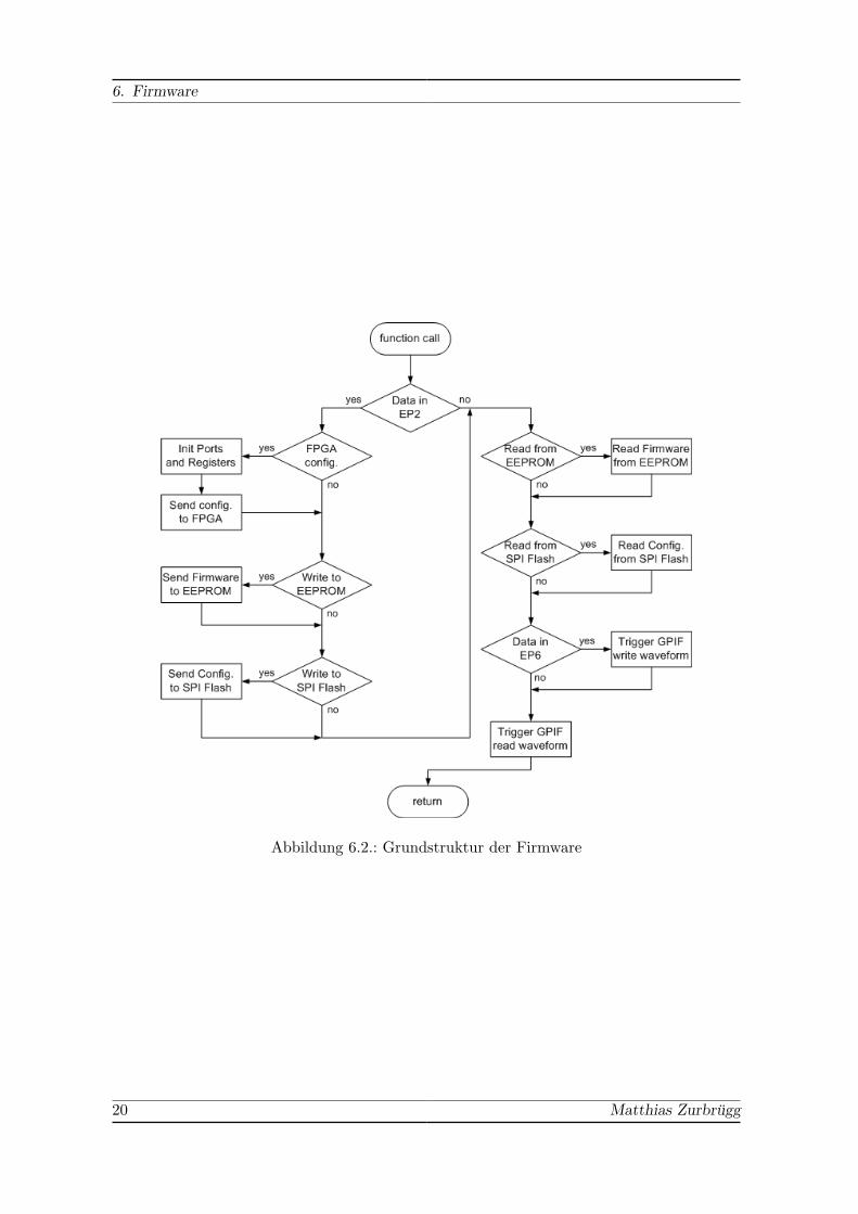
6.3. Grundstruktur der Firmware
Die eigentliche Hauptfunktion unserer Firmware ist TD Poll(), da dies vom Cypress Fra-mework so festgelegt wird. TD Poll() wird wie im Unterkapitel 6.1 erwahnt, regelmassigaufgerufen. Bei jedem Aufruf wird gepruft, ob Daten am EP2 bereitstehen. Falls das zu-trifft wird eine vom Vendor Request abhangige Aktion durchgefuhrt bzw. die entsprechendeFunktion aufgerufen. Danach wird der EP6 auf seinen Dateninhalt kontrolliert. Wenn Da-ten vorhanden sind, wird die GPIF Schreibefunktion fur einen Datentransfer zwischen demEP6 FIFO Buffer und dem FPGA gestartet. Am Schluss von TD Poll() wird noch die GPIFLesefunktion aufgerufen um zu schauen ob der FPGA Daten an den Host senden will. Dasin Abbildung 6.2 dargestellte Flussdiagramm zeigt den Programmablauf bei einem Aufrufvon TD Poll().
Project Report 19
6. Firmware
Abbildung 6.2.: Grundstruktur der Firmware
20 Matthias Zurbrugg

6.4. FPGA Konfiguration
6.4. FPGA Konfiguration
Es gibt mehrere Moglichkeiten den FPGA mit einem Mikrokontroller zu konfigurieren. Wirwahlten dafur den Slave Parallel Mode, da unser FPGA uber 16 Datenleitungen mit demEZ-USB FX2 verbunden ist. Je nach Literatur wird diese Konfigurationsart auch Select-MAP Mode genannt und ist im Application Note von Xilinx [NP02] erklart. Wichtig ist zubeachten, dass in diesem Modus die Daten Byte-Swapped uber die Datenleitungen gesen-det werden mussen. Dieses Problem wurde mit einer Hardwareanderung gelost und ist imUnterkapitel 3.1 schon beschrieben.
Der FPGA kann von der Firmware uber zwei Wege konfiguriert werden. Entweder mansendet die Konfiguration direkt vom Host uber USB zum FPGA oder der EZ-USB FX2 wirdim stand-alone Betrieb gestartet. In diesem Fall wird er die Firmware uber I2C in sein RAMladen. Anschliessend beschreibt die Firmware in der Initialisierungsphase den FPGA mitdem Inhalt des SPI Flashs. Dieser Konfigurationsvorgang wird im Kapitel 6.5 behandelt.Dieses Kapitel beschreibt nur die direkte Konfiguration vom Host.
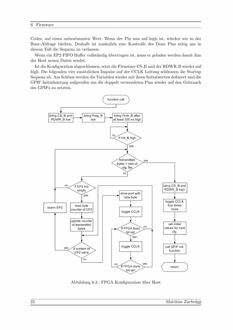
Die Konfigurationssequenz wird mit einem Vendor Request vom Host gestartet. Um wel-chen Request es sich dabei handelt, ist im Unterkaptiel 6.8 beschrieben. Manche Pins undRegister werden vom GPIF und der Konfigurationsfunktion verwendet. Per Default ist derEZ-USB FX2 fur die Verwendung des GPIFs initialisiert. Deshalb wird als erstes eine kleineFunktion aufgerufen, welche den EZ-USB FX2 zum Konfigurieren des FPGAs initialisiert.Erst jetzt wird die eigentliche Funktion fur die Konfiguration aufgerufen.
Zuerst bringt die Firmware den CS B und den RDWR B Pin low. Mit dem anschliessendenLoschen des Prog B Pins resetet man den FPGA. Nachdem Prog B wieder gesetzt wird, gehtder FPGA in den Configuration Load Modus. Dieser Zustand signalisiert der Spartan 3 mitdem setzen des INIT B Pins. Nun ist er bereit die Konfigurationsdaten zu empfangen.
Wahrend dieser Phase bleibt die Firmware in dieser Funktion, bis die Anzahl der vomUSB empfangenen Byte der Grosse der FPGA Konfigurationsdatei entspricht. Diese Dateisendet die Hostsoftware ohne Header und hat somit fur den selben FPGA Typ immer dieselbe Lange. Diese Lange muss jedoch im Sourcecode definiert werden. Nun wird festgestelltob Daten im EP2 vorhanden sind bzw. der Host neue Daten gesendet hat. Wenn dies zutrifft,liest die Firmware das Byte Counter Register des EP2 FIFO Buffers ein und aktualisiert denZahler, der die empfangenen Byte erfasst. Danach wird das erste Byte im FIFO Buffer an denDatenbus gelegt. Bei einem Impuls an der CCLK Leitung liest der Spartan 3 das Byte ein.Um das nachste Byte im FIFO Buffer auf den Datenbus zulegen, muss die Firmware keineAdresse inkementieren. Dies geschieht mit dem Autopointer bei jedem Zugriff automatisch.Unsere Firmware arbeitet beim EP2 und EP4 ausschliesslich mit diesem Feature. Die genaueFunktion des Autopointers ist im Technical Reference Manual [Cyp06] beschrieben.
Diese Sendesequenz wird nun solange wiederholt bis der Inhalt des FIFO Buffers ubert-ragen ist. Sollte der FPGA den Busy Pin setzten, ist ein weiterer Clock-Impuls notig undsolange zu wiederholen, bis er wieder bereit ist neue Daten anzunehmen. Der Busy-Checkist optional, da der FPGA mit einem schnelleren Takt arbeitet als der EZ-USB FX2. Somitwird es wahrscheinlich nie vorkommen, dass der Mikrokontroller den Spartan 3 uberfordert.Doch um eine zuverlassige Konfiguration zu garantieren haben wir die Abfrage des BusyPins dennoch implementiert.
Der Busy-Check wird uns jedoch am Ende der Konfiguration zum Verhangnis. Die letzten16 Byte der Datei sind Dummy-Information. Deshalb ist der FPGA schon vor dieser Sequenzfertig konfiguriert und treibt den Busy Pin, in Abhanigkeit der Pinbelegung des VHDL
Project Report 21
6. Firmware
Codes, auf einen unbestimmten Wert. Wenn der Pin nun auf high ist, wurden wir in derBusy-Abfrage bleiben. Deshalb ist zusatzlich eine Kontrolle des Done Pins notig um indiesem Fall die Sequenz zu verlassen.
Wenn ein EP2 FIFO Buffer vollstandig ubertragen ist, muss er geladen werden damit ihmder Host neuen Daten sendet.
Ist die Konfiguration abgeschlossen, setzt die Firmware CS B und der RDWR B wieder aufhigh. Die folgenden vier zusatzlichen Impulse auf der CCLK Leitung schliessen die StartupSequenz ab. Am Schluss werden die Variablen wieder mit ihren Initialwerten definiert und dieGPIF Initialisierung aufgerufen um die doppelt verwendeten Pins wieder auf den Gebrauchdes GPIFs zu setzten.
Abbildung 6.3.: FPGA Konfiguration uber Host
22 Matthias Zurbrugg

6.5. Stand-alone Betrieb
6.5. Stand-alone Betrieb
Die Firmware muss im EEPROM gespeichert werden, damit eine stand-alone Betrieb moglichist. Beim Aufstarten kontrolliert der Mikrokontroller uber I2C, ob eine bootfahige Firmwareim EEPROM vorhanden ist [Cyp06]. Bootfahig heisst der C-Code wird nicht im Intel Hex-Format gespeichert sondern im Binary Format. Dazu muss noch eine definierte Kopf- undFusszeile eingefugt werden. Um das Erstellen dieser Datei braucht sich der Programmierernicht zu kummern. Bei jeder Kompilation im µVision2 wird die kleine Cypress Softwarehex2bix.exe aufgerufen, welche die Hex-Datei umwandelt und als .iic Datei abspeichert.Dieser Vorgang ist im Angang C beschrieben.
6.5.1. EEPROM beschreiben
Mit dem entsprechenden Vendor Request startet man die Funktion zum Beschreiben desEEPROMs. Zuerst wird die Speicheradresse, von wo aus das EEPROM beschrieben werdensoll, auf 0 gesetzt. Danach verweilt die Firmware solange in der Funktion bis der EP2 keineDaten mehr erhalt. Es wird wieder die Anzahl Byte im FIFO Buffer eingelesen und im EP2Zahler gespeichert. Wenn dessen Inhalt grosser als 64 Byte ist, begrenzen wir die Schleife,die den EP2 Inhalt in das Array speichert, auf 64 Durchlaufe. Dies ist die maximal moglicheDatenmenge, die man mit einem sogenannten Page Write Befehl des EEPROMs ubertragendarf [Mic]. Das Zwischenspeichern in einem Array ist notig um mit der I2C Schreibefunktionvon Cypress arbeiten zu konnen. Die abgespeicherten 64 Byte werden jetzt von der gesamtAnzahl Byte im EP2 Zahler abgezahlt. Danach senden wir den Arrayinhalt uber den I2C undberechnen die neue Speicheradresse, von welcher aus beim nachsten Durchlauf der Sequenzdas EEPROM beschrieben werden soll. Wir haben beim ersten Durchlauf die Daten in dieSpeicheradressen 0 bis 63 geschrieben, folglich wird die nachste Adresse 64 sein. DieserVorgang wiederholt die Firmware solange bis der Wert im EP2 Zahler kleiner als 65 Byteist. Die Anzahl Durchlaufe der Speicherschleife wird nun auf den EP2 Zahlerwert gesetzt,da sowieso hochstens noch 64 Byte, also die maximal erlaubte Datenmenge, im FIFO Buffervorhanden sind. Wir speichern noch einmal den EP2 Inhalt in das Array und speichern ihnim EEPROM. Danach ist der Schreibevorgang aber noch nicht abgeschlossen sondern erstder FIFO Buffer ubertragen. Der EP2 wird wieder geladen und ist nun fur neue Daten vomHost bereit. Ist die Datei vollstandig im EEPROM gespeichert, erhalt der EZ-USB FX2vom Host einen entsprechenden Vendor Request als Bestatigung. Dieser setzt gleichzeitigdie Variabeln der Funktion auf ihre Initialwerte.
Project Report 23

6. Firmware
Abbildung 6.4.: EEPROM beschreiben
24 Matthias Zurbrugg

6.5. Stand-alone Betrieb
6.5.2. EEPROM auslesen
Zum Debuggen kann mit der Lesefunktion der Inhalt des EEPROMs ausgelesen und uberUSB zum Host gesendet werden. Dies ist jedoch erst mit dem EZ-USB Control Panel vonCypress moglich. Unsere Hostsoftware macht von dieser Funktion der Firmware noch keinenGebrauch. Wie immer startet ein Vendor Request den Lesevorgang. Im Initialisierungsmodewird definiert, dass das EEPROM von der Speicheradresse 0 ausgelesen werden soll. Danachmuss diese Adresse dem EEPROM mit einem Write-Befehl mitgeteilt werden. Nun lesenwir den Wert ein, der mit dem Vendor Request mitgesendet wird. Dieses Datenwort ent-spricht der Anzahl Byte, die der Anwender aus dem EEPROM auslesen will. Danach wirdder Lesemodus aktiviert. Das Prinzip des Auslesens beruht auf der im Unterkapitel 6.5.1 be-schriebenen Schreibesequenz und wird daher nicht mehr im Detail beschrieben. Der einzigeUnterschied ist, dass beim Lesen des EEPROMs die Datenmenge die man auf einmal lesendarf, nicht begrenzt ist. Es werden trotzdem nur 64Byte Pakete ausgelesen, damit man dasBuffer Array der Schreibefunktion verwenden kann. Wenn der EP4 FIFO Buffer mit dengewunschten Daten gefullt ist, laden wir ihn und setzen die Schreibefunktion wieder in denIdle Modus.
Abbildung 6.5.: EEPROM auslesen
Project Report 25
6. Firmware
6.6. FPGA Autokonfiguration
Ist der Gecko3 im stand-alone Modus, muss der FPGA automatisch von der Firmware be-schrieben werden. Seine Konfiguration ist dafur im SPI Flash abgelegt. Das automatischeKonfigurieren ist im Unterkapitel 6.6.3 beschrieben.
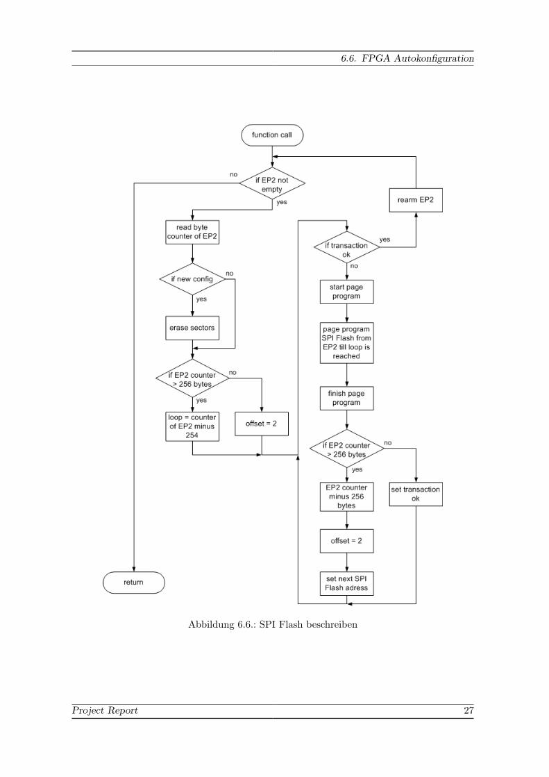
6.6.1. SPI Flash beschreiben
Um eine Konfiguration im SPI Flash zu speichern, startet der Host mit dem entsprechendenVendor Request diese Funktion. Danach kontrollieren wir ob Daten im EP2 FIFO Buffervorhanden sind. Wenn dieser Fall zutrifft, wird die Anzahl Byte im FIFO Buffer eingelesen.Handelt es sich um eine neue Konfiguration werden die dazu benotigten Sektoren im SPIFlash geloscht. Dies ist notig um uberhaupt in den Flash-Speicher schreiben zu konnen.Mit der Page Program Instruktion kann man dem SPI Flash maximal 256 Byte senden.Deshalb wird kontrolliert, ob der Inhalt im EP2 FIFO Buffer grosser als 256 Byte ist. Eskonnen hochstens 512Byte im FIFO Buffer vorhanden sein, also zwei mal eine Page ProgramInstruktion. Da jedoch die Start Page Program und Last Page Program Funktionen schon jeein Byte schreiben, muss die Page Programm Schleife zwei Byte weniger schreiben, weshalbein Offset notig ist. Die Schleife wird verlassen, wenn sie den Wert des FIFO Buffers minusden Offset erreicht hat. Sind also weniger als 256Byte im FIFO Buffer vorhanden, ist derOffset zwei. Wenn es jedoch mehr sind, muss der Offset mit Berucksichtigung auf die Limiteder 256 Byte berechnet werden. Wir starten nun die Page Program Instruktion, wiederholendiese bis die Schleifenbedingung erfullt ist und beenden sie mit einem Last Page Program.Sind es mehr Daten als 256 Byte, wird vom EP2 Bytezahler 256 subtrahiert und der Offsetauf 2 gesetzt, da sowieso hochstens noch einmal 256Byte vorhanden sein konnen. Danacherhoht die Firmware entsprechend der gesendeter Datenmenge die SPI Flash Adresse undwiederholt die Sequenz, bis die Ubertragung abgeschlossen ist. Bei Unklarheiten verweisenwir auf den gut kommentierten Sourcecode dieser Funktion, der im Anhang E.1.5 zu findenist. Die Abbildung 6.6 stellt dabei den strukturellen Ablauf dar.
26 Matthias Zurbrugg
6.6. FPGA Autokonfiguration
Abbildung 6.6.: SPI Flash beschreiben
Project Report 27
6. Firmware
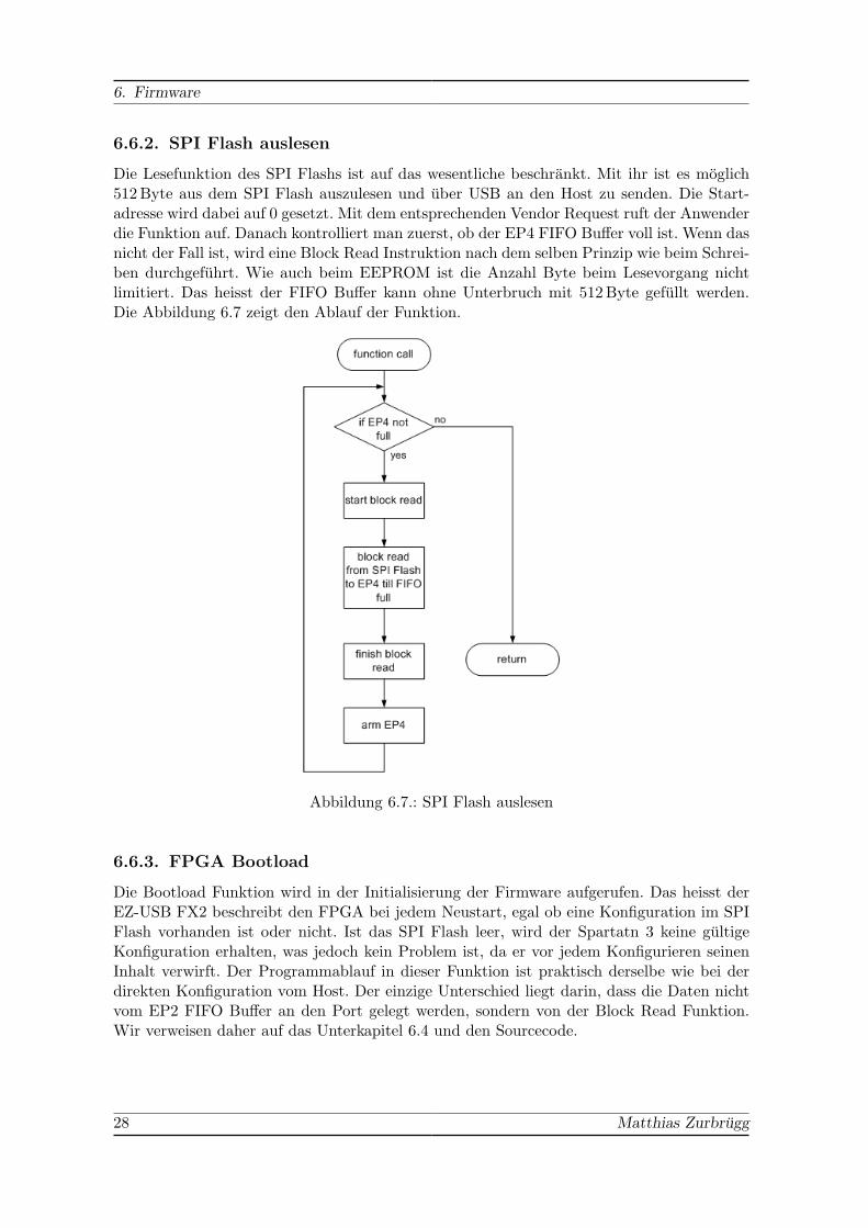
6.6.2. SPI Flash auslesen
Die Lesefunktion des SPI Flashs ist auf das wesentliche beschrankt. Mit ihr ist es moglich512 Byte aus dem SPI Flash auszulesen und uber USB an den Host zu senden. Die Start-adresse wird dabei auf 0 gesetzt. Mit dem entsprechenden Vendor Request ruft der Anwenderdie Funktion auf. Danach kontrolliert man zuerst, ob der EP4 FIFO Buffer voll ist. Wenn dasnicht der Fall ist, wird eine Block Read Instruktion nach dem selben Prinzip wie beim Schrei-ben durchgefuhrt. Wie auch beim EEPROM ist die Anzahl Byte beim Lesevorgang nichtlimitiert. Das heisst der FIFO Buffer kann ohne Unterbruch mit 512Byte gefullt werden.Die Abbildung 6.7 zeigt den Ablauf der Funktion.
Abbildung 6.7.: SPI Flash auslesen
6.6.3. FPGA Bootload
Die Bootload Funktion wird in der Initialisierung der Firmware aufgerufen. Das heisst derEZ-USB FX2 beschreibt den FPGA bei jedem Neustart, egal ob eine Konfiguration im SPIFlash vorhanden ist oder nicht. Ist das SPI Flash leer, wird der Spartatn 3 keine gultigeKonfiguration erhalten, was jedoch kein Problem ist, da er vor jedem Konfigurieren seinenInhalt verwirft. Der Programmablauf in dieser Funktion ist praktisch derselbe wie bei derdirekten Konfiguration vom Host. Der einzige Unterschied liegt darin, dass die Daten nichtvom EP2 FIFO Buffer an den Port gelegt werden, sondern von der Block Read Funktion.Wir verweisen daher auf das Unterkapitel 6.4 und den Sourcecode.
28 Matthias Zurbrugg

6.7. Kommunikation zwischen Host und FPGA
6.7. Kommunikation zwischen Host und FPGA
Fur die Kommunikation zwischen Host und FPGA werden, wie in Unterkaptiel 6.2 beschrie-ben, die Endpoints 6 und Endpoint 8 benutzt. Fur hohere Datenraten ist der 8051 Mikro-kontroller jedoch viel zu langsam. Cypress hat dafur ein General Propose Interface (GPIF)in den EZ-USB FX2 integriert, der die Arbeit fur schnelle Verbindungen ubernehmen soll.Die Abbildung 6.8 zeigt ein Blockdiagramm der Peripherie.
Abbildung 6.8.: GPIF
Das GPIF ist direkt mit dem USB verbunden und kann unabhangig vom Mikrokontrol-ler Daten bidirektional zwischen USB Endpoint und externer Peripherie austauschen. DerMikrokontroller ubernimmt dabei nur die Konfiguration des GPIFs und minimale Steuer-funktionen.
Das General Propose Interface ist eine Statemachine, die mit dem GPIF Designer vonCypress mit sogenannten Waveforms programmiert wird. Man kann im ganzen vier Wave-forms definieren, die jeweils bis zu sieben States haben. Das GPIF kennt vier verschiedenUbertragungsarten
• Single-Write Transaction um Steuerbefehle an die externe Peripherie zu ubermitteln
• Single-Read Transaction um Steuerbefehle von der externen Peripherie zu erhalten
• FIFO-Write und FIFO-Read Transaction um grosse Datenmengen mit der externenPeripherie auszutauschen
Wir benotigen nur die FIFO Transactions, da mit unserem Handshaking die externe Peri-pherie keine Steuerbefehle benotigt. Die Waveforms mussen der Transaktionsart zugewiesenwerden. In unserem Fall haben wir eine Waveform der FIFO-Read Transaction zugewie-sen um Daten vom FPGA zum USB zu ubermitteln. Fur die andere Richtung haben wireine Waveform als FIFO-Write Transaction definiert. Die zwei ubrigen Waveforms werdennicht verwendet. Uber den GPIF Designer kann man die Ein- und Ausgangessignale, dieWaveforms und dessen Transaktionsarten definieren. Beim anschliessenden Export in eineC-Datei sind keine weiteren Anderungen am erzeugten Programmcode notig. Es erstellteDatei (Gpif.c) muss lediglich in das µVision2 Projekt eingebunden und die darin enthalteneInitialisierung aufgerufen werden. Hinweise zur Verwendung des GPIF Designers sind imAnhang D zu finden.
Project Report 29

6. Firmware
6.7.1. Read Waveform
Bevor die Firmware die Read Waveform aufruft, kontrollieren wir ob sich das GPIF imIdle Status befindet. Das interne FIFO Flag im GPIF wird dann so eingestellt, dass esder EP6 FIFO Buffer setzt wenn er voll ist. Erst jetzt wird die Read Waveform gestartet.Solange die Firmware kein Timeout auslost, warten wir auf das Done Bit vom GPIF. DasInterface setzt dieses Bit falls es von einer Waveform in den Idle Status zuruckkehrt. Verweiltdie Statemachine zulange im selben Status wird der Timeout ausgelost und die Waveformabgebrochen. Somit erzwingt man ein Setzen des Done Bits. Dies geschieht regelmassig, dadie Read Waveform periodisch aufgerufen wird, um zu kontrollieren ob der FPGA Datensenden will. Sendet er nichts bleibt die Waveform solange im S0 Status bis das Timeout sieabbricht. Das General Propose Interface ubernimmt das gesammte USB Handling. Erst amEnde der Ubertragung muss der Endpoint, falls der FIFO Buffer nicht gefullt ist, von derFirmware geladen werden. In der Abbildung 6.9 ist die GPIF Read Funktion der Firmwaredargestellt.
Abbildung 6.9.: GPIF Read Funktion der Firmware
Im Ruhezustand kontrolliert das GPIF in der Read Waveform ob das WRX gesetzt wurde.Wenn das nicht der Fall ist, bricht die Firmware die Waveform wieder ab. Will der FPGAjedoch etwas senden, so prufen wir zuerst, ob der EP8 FIFO Buffer nicht voll ist. Danach
30 Matthias Zurbrugg
6.7. Kommunikation zwischen Host und FPGA
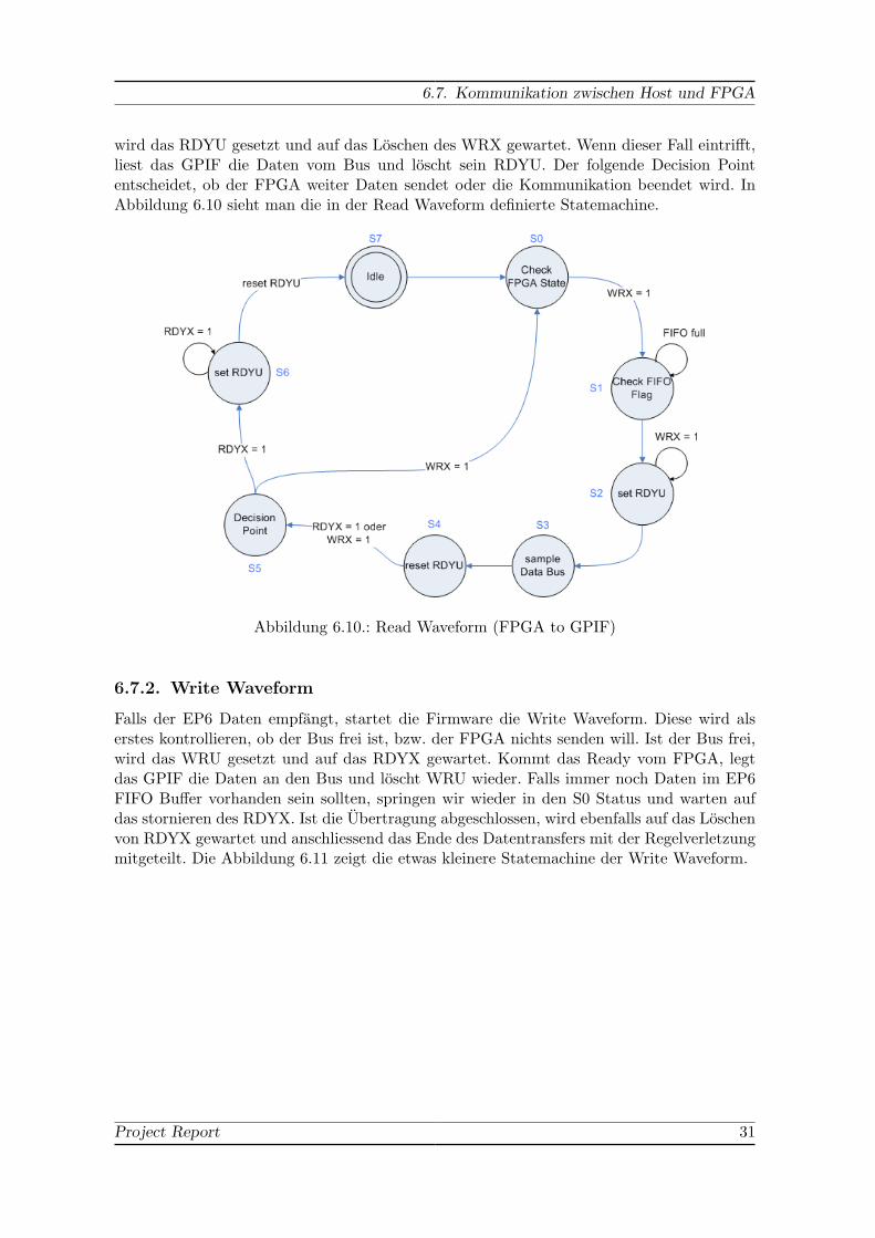
wird das RDYU gesetzt und auf das Loschen des WRX gewartet. Wenn dieser Fall eintrifft,liest das GPIF die Daten vom Bus und loscht sein RDYU. Der folgende Decision Pointentscheidet, ob der FPGA weiter Daten sendet oder die Kommunikation beendet wird. InAbbildung 6.10 sieht man die in der Read Waveform definierte Statemachine.
Abbildung 6.10.: Read Waveform (FPGA to GPIF)
6.7.2. Write Waveform
Falls der EP6 Daten empfangt, startet die Firmware die Write Waveform. Diese wird alserstes kontrollieren, ob der Bus frei ist, bzw. der FPGA nichts senden will. Ist der Bus frei,wird das WRU gesetzt und auf das RDYX gewartet. Kommt das Ready vom FPGA, legtdas GPIF die Daten an den Bus und loscht WRU wieder. Falls immer noch Daten im EP6FIFO Buffer vorhanden sein sollten, springen wir wieder in den S0 Status und warten aufdas stornieren des RDYX. Ist die Ubertragung abgeschlossen, wird ebenfalls auf das Loschenvon RDYX gewartet und anschliessend das Ende des Datentransfers mit der Regelverletzungmitgeteilt. Die Abbildung 6.11 zeigt die etwas kleinere Statemachine der Write Waveform.
Project Report 31

6. Firmware
Abbildung 6.11.: Write Waveform (GPIF to FPGA)
32 Matthias Zurbrugg

6.7. Kommunikation zwischen Host und FPGA
Die Write Funktion der Firmware unterscheidet sich, wie man in der Abbildung 6.12 er-kennen kann, nur im Endpoint von der Read Funktion und wird daher nicht weiter erlautert.
Abbildung 6.12.: GPIF Write Funktion der Firmware
Project Report 33

6. Firmware
6.7.3. Datenrate
Wie schon im Unterkapitel 3.1 angetont, lauft die Kommunikation mit 8 Bit Busbreite. VomGPIF ware eine Busbreite von 16 Bit moglich. Bei der Implementation der Firmware auf demGecko3 kann dies jedoch schnell im Register EPxFIFOCFG oder mit dem GPIF Designer(Wordwide Modus) umgestellt werden [Cyp06]. Um die Datenrate ungefahr voraussagen zukonnen, habe wir Messungen mit dem Logic Analyser gemacht. Die Abbildung 6.13 zeigtden Downstream (Host zu FPGA) von 512Byte. Mit den Markern lesen wir eine Zeit von90.24µs fur diese Datenlange mit der Abbruchbedingung heraus.
Abbildung 6.13.: Downstream von 512 Byte
Die folgende Berechnung der Datenrate geht von einem 16 Bit breiten Bus aus.
Anzahl ubertragene Bit: 512 Byte · 8 Bit/Byte · 2 = 8192Bit (6.1)
Datenrate:8192 Bit90.24 µs
= 90.78 MBit/s (6.2)
34 Matthias Zurbrugg
6.7. Kommunikation zwischen Host und FPGA
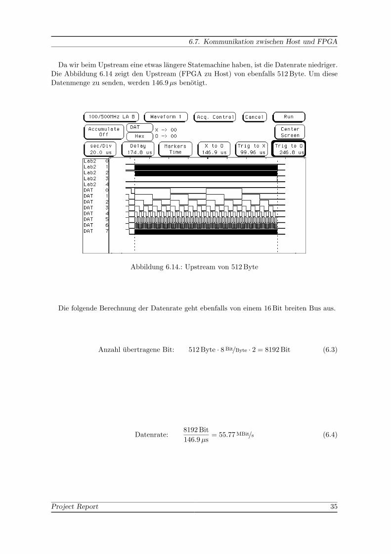
Da wir beim Upstream eine etwas langere Statemachine haben, ist die Datenrate niedriger.Die Abbildung 6.14 zeigt den Upstream (FPGA zu Host) von ebenfalls 512 Byte. Um dieseDatenmenge zu senden, werden 146.9µs benotigt.
Abbildung 6.14.: Upstream von 512Byte
Die folgende Berechnung der Datenrate geht ebenfalls von einem 16Bit breiten Bus aus.
Anzahl ubertragene Bit: 512 Byte · 8 Bit/Byte · 2 = 8192Bit (6.3)
Datenrate:8192 Bit146.9 µs
= 55.77 MBit/s (6.4)
Project Report 35

6. Firmware
6.8. Vendor Requests
Der Host verwendet Vendor Requests um der Firmware mitzuteilen, welche Funktion erausfuhren will. Diese werden, wie schon in der Abbildung 4.1 dargestellt, uber den Endpoint0 gesendet. Der Endpoint 0 ist besitzt einen bidirektionalen 64 Byte grossen Buffer. Wirhaben folgende Vendor Requests definiert:
• C1: Host sendet eine FPGA Konfiguration
• C2: EEPROM mit einer Firmware beschreiben
• C3: wahlbare Anzahl Byte vom EEPROM lesen (zum Debuggen)
• C4: SPI Flash mit einer Konfiguration beschreiben
• C5: 512 Byte aus dem SPI Flash lesen (zum Debuggen)
• C6: Bestatigung vom Host, dass Daten komplett gesendet wurden
• B1: Verlangt die Ruckgabe der Firmware Version
• B2: Verlangt die Ruckgabe des Done Bits nach einer Konfiguration
Wie der Ablauf von Vendor Requests und die anschliessende Datenubertragung aussieht,zeigt das Kaptiel 7.
36 Matthias Zurbrugg

7. Hostsoftware
Der aus Sicht des Anwenders wichtigste Teil unserer Arbeit ist die Host PC Software, daer mit ihr das Gecko Board in Betrieb nehmen kann und sie ihm einen moglichst einfachenWeg bereitstellt mit dem Gecko Board Daten auszutauschen.
Fur den Anwender gibt es die folgenden Aufgaben, die unsere Hostsoftware erfullen muss:
• Direkte Konfiguration des FPGAs
• Download einer FPGA Konfigurationsdatei fur den stand-alone Betrieb
• Moglichkeit um mit dem FPGA Daten auszutauschen
Der Datenaustausch wird von den anderen Aufgaben getrennt betrachtet. Dies ist sinnvoll,weil der Datenaustausch in den meisten Fallen auf die Applikation abgestimmt ist und dieDaten vielfach zuerst weiterverarbeitet werden sollen.
Dies haben wir schon im Konzept der USB Kommunikation einfliessen lassen und diebeiden unterschiedlichen Falle Administration und Kommunikation logisch voneinander ge-trennt. Wie im Kapitel 6 und in der Abbildung 6.1 beschrieben wird, sind fur diese Fallegetrennte Interfaces vorhanden. Aus Sicht des Host verhalt sich ein USB Gerat mit meh-reren Interfaces wie einzelne getrennte Gerate. So ist es in unserem Fall moglich, fur dieKommunikation und die Administration separate Software einzusetzen, ohne dass sich diesegegenseitig blockieren.
Fur die Hostsoftware weitere wichtige Anforderungen:
• Plattformubergreiffend einsetzbar, mindestens unter Linux und Windows
• Moglichst einfach in der Benutzung
• Kommunikation mit dem FPGA moglichst transparent
• Anwender soll sich nicht um die USB Schnittstelle kummern mussen
• Beispielprogramme sollen dem Anwender den Einstieg vereinfachen
• Aktualisieren der Firmware des EZ-USB FX2 mit der Hostsoftware moglich
7.1. Planung
Um diese Anforderungen unter einen Hut zu bringen war etwas mehr Planung notig umzu entscheiden welche Entwicklungswerkzeuge, Programmiersprache und Bibliotheken ge-nutzt werden sollen. Da es sich um eine plattformubergreiffende Entwicklung mit graphi-scher Oberflache handelt, musste zuerst ein GUI Framework gesucht werden, dass auf meh-reren Plattformen verfugbar ist. Dabei fiel die Wahl schnell auf Qt von der Firma Trolltech
Project Report 37

7. Hostsoftware
(www.trolltech.com), da dieses auf Windows, Linux und MacOS X verfugbar ist, sehr aus-gereift ist und wir von der Erfahrung von Andreas Eicher, Assistent im Microlab, profitierenkonnten. Qt ist ein Framework fur C++, so stand auch die Programmiersprache fest. Javawar keine Option, weil die USB Schnittstelle nicht unterstutzt wird.Qt wird von Trolltech unter verschiedenen Lizenzen angeboten. Eine Variante ist die GNUPublic License (GPL), die einen Entwickler dazu zwingt ein Projekt, das GPL Software be-nutzt, auch unter die GPL zu stellen und mit allen Sourcecodes zu veroffentlichen. Qt wirdnur in der Version 4 und hoher auch auf Windows unter der GPL angeboten. Die andereVariante ist eine kommerzielle Lizenz, die von Trolltech erworben werden kann. Damit mussder Sourcecode eines Projektes nicht veroffentlicht werden. Zur Zeit wird von uns Qt 4.1.2 inder GPL Version benutzt aber die Frage der Veroffentlichung unserer Software konnte nochnicht geklart werden.
Um zu verhindern, dass unter Linux ein eigenes Kernelmodul entwickelt werden muss,greiffen wir auf die libusb zuruck (libusb.sourceforge.net, Version 0.1.12), ein Open-SourceProjekt unter der LGPL. Die LGPL erlaubt eine uneingeschrankte Verwendung in eigenenProjekten aber Anderungen an der libusb mussen veroffentlicht werden. Mit der libusb kanndirekt aus einem Anwenderprogramm auf USB Gerate zugegriffen werden. Folgende Platt-formen werden unterstutzt: Linux, *BSD und MacOS XFur Windows existiert ein anderes Projekt (libusb-win32.sourceforge.net), das die libusbportiert hat und die selbe API besitzt. So ist es theoretisch moglich, unsere Hostsoftwareauf Windows, Linux und MacOS X einzusetzen. Die Software wurde unter Linux entwickeltund getestet. Leider reichte die Zeit nicht aus, die Portierbarkeit unserer Software und derlibusb zu testen.Unter Windows steht als Option weiterhin die Entwicklung eines eigenen Treibers zur Ver-fugung, da von Cypress dazu Beispiele vorhanden sind. Dies erleichtert den Einstieg in dieTreiberprogrammierung enorm.
7.2. Realisierung
Da keiner von uns Erfahrung in der C++ Programmierung hatte, mussten wir in kurzer Zeiteinen Uberblick bekommen. Dabei war uns Andreas Eicher und das Buch [Bre03] behilflich.
Die Hostsoftware wurde in mehrere Klassen und mehrere Applikationen unterteilt. Daszentrale Element ist die QGecko Klasse. Sie ist von der Klasse QObject, der Grundklassedes Qt Frameworks, abgeleitet. Sie stellt alle Funktionen bereit, die zur Administration undKommunikation mit dem Gecko Board benotigt werden. Die USB Zugriffe sind vollstandiggekapselt.
Aufbauend auf dieser Klasse wurden zwei Applikationen erstellt: Der Gecko Administra-tor und das Simplecom. Der Gecko Administrator stellt ein graphisches Interface fur alleadministrativen Aufgaben des Gecko Boards zur Verfugung. Das Simplecom diente uns zumtesten der Kommunikation mit dem FPGA und zeigt, wie einfach eine Applikation mit demFPGA Daten austauschen kann. Der Sourcecode vom Simplecom dient als Beispiel zur Ver-wendung der QGecko Klasse zur Kommunikation mit dem Gecko Board. Die Sourcecodessind im Anhang E.3 zu finden.
Die implementierten Funktionen der Hostsoftware wurden getestet und funktionierten.Ein kurzer Blindtest, von Personen die die Software noch nicht kannten, hat ergeben, dasssie keine Fehlfunktion auslosen konnten. Limitierend ist zur Zeit einzig, dass unter Linux
38 Christoph Zimmermann
7.3. Gecko Library
bisher Root Rechte notig sind. Es existieren unter Linux mehrere Moglichkeiten um dieZugriffsrechte von USB Geraten zu beeinflussen. Die derzeit aktuelle und flexibelste Losungin diesem Zusammenhang ist der udev Damon, der alle zur Laufzeit hinzugefugten bzw.entfernten Gerate verwaltet. Einer der nachsten Schritte in der Entwicklung der Hostsoftwareunter Linux sollte es sein, udev so zu konfigurieren, dass alle Studenten auf den Geckozugreiffen konnen.
7.3. Gecko Library
In diesem Unterkapitel werden die von der Gecko Library zur Verfugung gestellten Funktio-nen beschrieben und erklart wie sie das Gecko Board ansteuern. Die Namen der Funktionensind so gewahlt, dass man sofort sieht ob sie zur Kommunikation oder Administration (be-ginnen immer mit adm) dienen. Alle Funktionen liefern als Ruckgabewert einen Binarwertzuruck der aussagt, ob die Funktion erfolgreich war oder nicht.
• bool open()Diese Funktion offnet eine Kommunikationsverbindung zum Gecko Board.Sie entspricht mehrheitlich dem Beispiel in der libusb Dokumentation zum Suchen undOffnen eines USB Gerates. Als erstes werden alle USB Busse und dann alle Gerate neueingelesen. Danach wird mit den so erhaltenen Informationen nach der Vendor undProduct ID des Gecko Boards gesucht. Bei Erfolg wird ein allfalliger Linux KernelTreiber entfernt und das Interface zur Kommunikation geoffnet. Die Funktion brichtnach dem ersten Fund ab, es ist mit dieser Funktion nicht moglich mehrere GeckoBoards am gleichen Rechner parallel zu betreiben.
• bool close()Schliesst eine geoffnete Kommunikationsverbindung mit dem Gecko Board, wenn einesolche existiert.
• bool read(QByteArray *readData, int byteCount)Funktion um die im Parameter byteCount angegebene Anzahl Bytes vom Gecko Boardzu lesen und setzt diese Daten ans Ende des zur Verfugung gestellten QByteArrays.Das ByteArray muss existieren.Die Funktion fuhrt einen einfachen Bulkread auf dem Kommunikationsinterface aus.
• bool write(QByteArray data)Funktion um die Daten in einem QByteArray an das Gecko Board zu senden.Die Funktion fuhrt einen einfachen Bulkwrite auf dem Kommunikationsinterface aus.
• bool write(QFile &data)Funktion um den Inhalt eines ganzen Files an das Gecko Board zu ubertragen. DasFile muss existieren und geoffnet sein. Am Ende der Funktion zeigt der Filepointer aufdas Ende des Files.Da die Bulkwrite Funktion der libusb nur einen Integerwert fur die Anzahl Bytesbenutzt, muss die Ubertragung eines ganzen Files in mehrere Transaktionen aufgeteiltwerden.
• bool admOpen()Funktion zum Offnen einer Administrationsverbindung zum Gecko Board.
Project Report 39

7. Hostsoftware
Funktioniert genau so wie die open() Funktion mit dem Unterschied, dass das Admi-nistrationsinterface geoffnet wird.
• bool admClose()Schliesst eine geoffnete Administrationsverbindung mit dem Gecko Board, falls eineexistiert.
• bool admConfigure(QFile &configData)Funktion um den FPGA auf dem Gecko Board zu konfigurieren. Das File muss einekorrekte Konfigurationsdatei ohne Header Informationen sein. Das File muss existierenund geoffnet sein.Um den FPGA zu konfigurieren muss zuerst der entsprechende Vendor Request gesen-det werden (siehe dazu Unterkapitel 6.8) und im Anschluss die Konfigurationsdaten.Nach dem alle Daten der Konfigurationsdatei gesendet sind, muss ein Vendorrequestgesendet werden, der den Abschluss bestatigt.
• bool admDownload(QFile &configData, int place)Funktion zum Download von FPGA Konfigurationsdateien fur den stand-alone Be-trieb des Gecko Boards. Das File muss eine korrekte Konfigurationsdatei ohne HeaderInformationen sein. Das File muss existieren und geoffnet sein. Der Parameter placegibt an, welcher Konfigurationsplatz beschrieben werden soll. Auf dem Gecko Boardkonnen mehrere Konfigurationen parallel gespeichert werden und per Schalter aus-gewahlt werden, welche geladen werden soll. Die Konstante GECKO MAX CONFIGSdie in dieser Library definiert ist, gibt an wie viele Platze zur Verfugung stehen.Der Ablauf ist der selbe wie bei der Konfiguration des FPGA, es werden nur andereVendor Requests gesendet.
• bool admFirmware(QFile &configData)Funktion um eine neue Firmware fur den EZ-USB FX2 auf das Gecko Board zu laden.Die Firmware wird in das EEPROM geschrieben und wird nach einem Reset des EZ-USB FX2 gestartet. Das File muss ein korrektes Firmware File im Format *.iic sein(siehe dazu Unterkapitel 6.5). Wie bei den anderen Funktionen muss das File existierenund geoffnet sein.Die Funktion sendet den Vendor Request zum Senden einer Firmware, danach werdendie Daten aus dem Firmware File gesendet und am Schluss der Vendor Request zurBestatigung, dass alle Daten gesendet wurden.
• bool admGetFwVersion(QString *version)Funktion zum Abfragen der Versionsnummer der EZ-USB FX2 Firmware. Der QStringmuss existieren. Die Versionsnummer ist im Format X.XX und wird dem String an-gehangt.Die Versionsnummer wird gelesen indem ein Vendor Request gesendet wird, der denEZ-USB FX2 auffordert vier Bytes zuruck zu senden. Dazu wird der Vendor Requestmit der Bitmaske verknupft die das Bit fur eine Lesetransaktion setzt.
Diese Funktionsbibliothek sollte spater als dynamische Library kompiliert werden undsystemweit verfugbar gemacht werden.
40 Christoph Zimmermann

7.4. Gecko Administrator
7.4. Gecko Administrator
Der Gecko Administrator (Dateiname ist geckoadm) stellt eine graphische Benutzerober-flache zur Benutzung des Gecko Boards zur Verfugung. Das GUI ist schlicht gehalten. Dieeinzelnen Funktionen werden in separaten Tabbs angeordnet um die Ubersichtlichkeit zuerhohen. Wenn die Applikation normal gestartet wird, stehen folgende Funktionen zur Aus-wahl:
• FPGA Konfiguration (Abbildung 7.1)
• Download Konfiguration (Abbildung 7.2)
• Informationsseite mit der Versionsnummer, Autoren etc. (Abbildung 7.4)
Abbildung 7.1.: GUI zur FPGA Konfigura-tion
Abbildung 7.2.: GUI zum Download derKonfigurationsdatei
Abbildung 7.3.: GUI zum Aktualisieren derFirmware
Abbildung 7.4.: Informationsseite des GeckoAdministrators
Wenn die Applikation mit der Kommandozeilenoption “−−firmware” gestartet wird, kannauch die EZ-USB FX2 Firmware aktualisiert werden und die Version abgefragt werden (Ab-bildung 7.3). Diese Funktion wird normalerweise nicht angezeigt um zu verhindern, dass ein
Project Report 41
7. Hostsoftware
Benutzer versehentlich eine Aktualisierung macht mit einer falschen Firmware und so dasGecko Board nicht mehr mit unserer Hostsoftware benutzt werden kann. Nach solch einemMissgeschick kann eine korrekte Firmware unter Windows mit dem Cypress EZ-USB ControlPanel oder unter Linux mit dem Programm fxload heruntergeladen werden.
Die typischen Fehler des Benutzers werden vom Gecko Administrator abgefangen. Entwe-der es wird ein Hinweisfenster angezeigt oder eine Meldung in die Statuszeile geschrieben.Wenn eine Funktion nicht ordnungsgemass ausgefuhrt werden konnte, wird dies ebenfalls inder Statusleiste angezeigt. Die vom Benutzer zuletzt verwendeten Dateien und Pfade wer-den beim Beenden gespeichert und der Anwender kann beim nachsten Start der Applikationgleich weiterarbeiten. Die USB Kommunikation wird vor jedem Funktionsaufruf neu geoffnetund am Ende wieder geschlossen. Die Applikation muss also nicht geschlossen werden, wenndas Gecko Board vom Host PC getrennt wird.
7.5. Beispielprogramm: Simplecom
Diese Applikation zeigt die Verwendung der Gecko Library um eigene Software zu program-mieren, die mit dem Gecko Board Daten austauscht.
Im Konstruktor wird das GUI erstellt und die Kommunikation mit dem Gecko Boardinitialisiert. Dazu muss eine Instanz der QGecko Klasse erstellt werden, danach kann mitder Funktion open() die USB Kommunikation geoffnet werden.Der Rest zeigt, wie einfach Dateien gesendet und Daten gelesen werden konnen. Im GUIwerden die Daten als hexadezimale Zahlen dargestellt.
Das Simplecom ist kein vollstandiges Programm, da einige Sicherheitsabfragen und Ele-mente der Fehlerbehandlung fehlen. Es erfullt aber den Zweck als Beispiel fur eigene Projekte.
42 Christoph Zimmermann

8. Ausblick
Dieses Kapitel soll den weiteren Projektverlauf aufzeigen.
8.1. Weiteres Vorgehen
8.1.1. Firmware
• Planung und Realisation eines Protokolls, das im Kommunikationsmodus die Da-tenlange die der FPGA senden will, dem Host mitteilt.
• GPIF auf 16 Bit Busbreite konfigurieren
• Schalter uber I2C einlesen, der bestimmt von welchem Teil des SPI Flashs die Konfi-guration geladen wird
• Status der Firmware uber I2C an LEDs ausgeben
• Das nichtsetzen des FIFO Buffer Full Flags analysieren
• Wenn notig EEPROM und SPI Flash Lesefunktionen ausbauen
• FPGA Typ von Firmware auslesen, damit die Grosse der Konfigurationsdatei nichtmehr manuell im C-Code definiert werden muss
8.1.2. Hostsoftware
• Windows Portierung
• Test mit USB 1.1, da wahrend unserer Arbeit kein USB 1.1 Hub zur Verfugung stand
• Test auf 64 Bit Computern und Betriebssystemen
• Flash und EEPROM auslese Funktionen
• Entwicklung einer Applikation um das Intel NOR Flash zu beschreiben
8.1.3. FPGA Cores
• Ansteuerung des Intel NOR Flashs
• Bei Bedarf verbesserung der Testroutinen
• Entwicklung eines einfachen Referenzsystems
• Schreiben von Testroutinen fur die weiteren Funktionsblocke
Project Report 43

8. Ausblick
8.1.4. Gecko3 Hardware
• Validierung des Schemas
• Layouten der Leiterplatte
• Post-route Simulation der DDR-RAM Verbindungen
• Aufbau, Test und Messungen des Prototyps
• Planung der Produktion einer Kleinserie
44 Matthias Zurbrugg, Christoph Zimmermann

9. Schlusskapitel
Die Gecko3 Softwareentwicklung war ein sehr abwechslungsreiches Projekt, das uns denEinblick auf das Zusammenwirken verschiedener Programmiersprachen auf verschiedenenPlattformen und die Verwendung mehrerer Bussysteme gewahrte.
Cypress ist uns dabei in etwas schlechter Erinnerung geblieben. Ihr falsch verdrahtetesD-Sub Kabel oder die Beispiele, die nur mit einer alteren Version des Control Panels funk-tionieren, haben wesentlich zu ihrem getrubten Ruf bei uns beigetragen.
Doch Dank unserem guten Teamgeists konnten etliche Fragen beantwortet und die Pro-bleme gelost werden. Somit war es moglich das Projekt erfolgreich abzuschliessen.
18. Dezember 2006, Biel/Bienne
Matthias Zurbrugg Christoph Zimmermann
.......................................... ..........................................
Project Report 45

Anhang
46 Matthias Zurbrugg, Christoph Zimmermann

A. Projekt- und Zeitplanung
Project Report 47
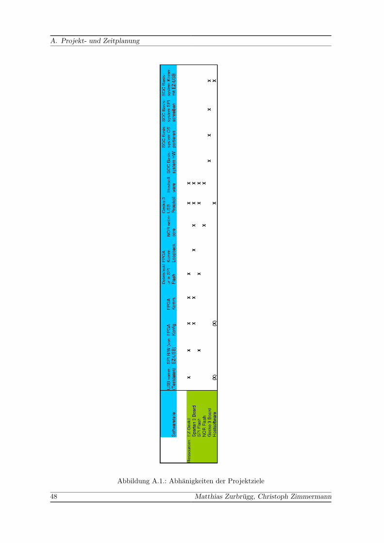
A. Projekt- und Zeitplanung
Abbildung A.1.: Abhanigkeiten der Projektziele
48 Matthias Zurbrugg, Christoph Zimmermann

A. Projekt- und Zeitplanung
Novem
ber
23
24
25
26
27
28
29
30
31
12
34
56
78
910
11
12
13
14
15
16
17
18
19
20
21
22
23
24
25
26
27
28
29
30
12
34
56
78
910
11
12
13
14
15
16
17
18
NO
R w
rite
r core
Overa
ll T
esting
Adm
inis
tration
Okto
be
rD
eze
mb
er
Pro
jektp
lan
un
g
Ein
rich
tun
g
Entw
icklu
ngs-
um
ge
bun
g
Entw
icklu
ngsh
ard
-w
are
SP
I ein
arb
eite
n
SP
I R
/W (
vo
n E
Z-
US
B)
GP
IF e
ina
rbe
iten
US
B k
om
m.
(Te
std
ate
n)
FP
GA
Kon
fig
.
FP
GA
Kom
m.
Da
teis
tru
ktu
r in
S
PI F
lash
FP
GA
Kom
m.
Lo
opb
ack
US
B L
inu
x
ein
arb
eite
n
US
B W
ind
ow
s
ein
arb
eite
n
Ge
cko 3
US
B
Pro
toko
ll
Pla
nu
ng
Ho
st S
W
Ho
sts
oftw
are
Do
ku
me
nta
tio
n
Sche
ma
ko
rre
ktu
r-e
n
La
you
tbe
tre
uu
ng
Abse
nze
n
Ch
. Z
imm
erm
an
n
M. Z
urb
rüg
g
Abbildung A.2.: Soll Zeitplan
Project Report 49

A. Projekt- und Zeitplanung
No
ve
mb
er
23
24
25
26
27
28
29
30
31
12
34
56
78
910
11
12
13
14
15
16
17
18
19
20
21
22
23
24
25
26
27
28
29
30
12
34
56
78
910
11
12
13
14
15
16
17
18
NO
R w
rite
r co
re
EZ
-US
B F
irm
wa
re
Ove
rall
Te
sting
Ad
min
istr
ation
Ch
. Z
imm
erm
ann
Okto
be
rD
ezem
be
r
Pro
jektp
lan
un
g
Ein
rich
tun
g
En
twic
klu
ngs-
um
ge
bu
ng
En
twic
klu
ngsha
rd-
wa
re
SP
I e
ina
rbe
ite
n
SP
I R
/W (
vo
n E
Z-
US
B)
GP
IF e
ina
rbeiten
US
B k
om
m.
(Te
std
ate
n)
FP
GA
Ko
nfig
.
FP
GA
Ko
mm
.
Da
teis
tru
ktu
r in
SP
I F
lash
I2C
EE
PR
OM
a
nste
ue
rn
FP
GA
Ko
mm
. L
oo
pb
ack
US
B L
inu
x
ein
arb
eite
n
US
B W
ind
ow
s
ein
arb
eite
n
Gecko
3 U
SB
P
roto
ko
ll
Pla
nu
ng
Ho
st
SW
Ho
sts
oft
ware
Do
kum
en
tation
Sche
ma
ko
rre
ktu
ren
Layo
utb
etr
eu
ung
Ab
se
nze
n
M.
Zu
rbrü
gg
Abbildung A.3.: Ist Zeitplan
50 Matthias Zurbrugg, Christoph Zimmermann

B. Definition der Verbindung desSpartan3 Boards mit dem EZ-USBFX2 Board
Project Report 51

B. Definition der Verbindung des Spartan3 Boards mit dem EZ-USB FX2 Board
Pin
onE
Z-U
SBFX
2P
inon
EZ-U
SBD
ev-kitN
ame
inSchem
aticD
irectionC
ase:C
onfigurationof
FP
GA
Case:
SoC-
Host
Pin
onSpartan3
FT
256P
inon
Connector
B1
FD
0P
1.19D
0I/O
D7
Data
0M
619
FD
1P
1.18D
1I/O
D6
Data
1N
617
FD
2P
1.17D
2I/O
D5
Data
2R
715
FD
3P
1.16D
3I/O
D4
Data
3T
713
FD
4P
1.15D
4I/O
D3
Data
4R
1011
FD
5P
1.14D
5I/O
D2
Data
5P
109
FD
6P
1.13D
6I/O
D1
Data
6N
117
FD
7P
1.12D
7I/O
D0
Data
7M
1140
FD
8P
1.11D
8I/O
unusedD
ata8
C15
21FD
9P
1.10D
9I/O
unusedD
ata9
D15
23FD
10P
1.9D
10I/O
unusedD
ata10
E15
25FD
11P
1.8D
11I/O
unusedD
ata11
F15
27FD
12P
1.7D
12I/O
unusedD
ata12
G16
29FD
13P
1.6D
13I/O
unusedD
ata13
H16
31FD
14P
1.5D
14I/O
unusedD
ata14
K16
33FD
15P
1.4D
15I/O
unusedD
ata15
L15
35
PA7
P2.12
DO
NE
toE
Z-U
SBD
onelocked*
R14
37R
DY
0&
PA4
P2.5
&P
2.15IN
ITB
/WR
Xto
EZ-U
SBIN
ITB
WR
XN
938
PA5
P2.14
PR
OG
Bto
FP
GA
Prog
Blocked*
B3
36C
TL1
P2.10
RD
WR
B/W
RU
toFP
GA
RD
WR
BW
RU
T3
5C
TL2
P2.9
CS
B/R
DY
Uto
FP
GA
CS
BR
DY
UR
320
RD
Y1
P2.4
BU
SY/R
DY
Xto
EZ-U
SBB
usyR
DY
XP
9A
1.20C
TL0
P2.11
CC
LK
toFP
GA
CC
LK
locked*T
1539
PK
TE
ND
P2.13
PK
TE
ND
toE
Z-U
SBunused
PK
TE
ND
C10
4
*don’ttouch
Done/P
rogramlines
-w
oulddelete
Configuration!!
9.11.2006,zim
mc5
Tabelle
B.1.:
Definition
derV
erbindungzw
ischendem
Spartan3
StarterK
itund
demE
Z-U
SBFX
2LP
Developm
entK
it
52 Christoph Zimmermann

C. Hex to Bix
Damit der EZ-USB FX2 die Firmware auf dem EEPROM als bootfahig erkennt, muss sie, wieschon im Unterkapitel 6.5 erwahnt, ein spezielles Format haben. Im vorbereiteten µVision2Projekt von Cypress ist der Kompiler schon so konfiguriert, dass er bei jeder Kompilationnoch eine Software startet, die die Hex-Datei ins Binary-Format umwandelt, Kopf- undFusszeile hinzufugt und als iic-Datei abspeichert.Die Abbildung C.1 zeigt wo diese Software im µVision2 unter Options for Target eingebundenwerden kann.
Abbildung C.1.: Starten einer zusatzlichen Software nach der Kompilation
Neben dem Programmaufruf werden noch etliche Parameter mitgegeben. Unsere Parame-terliste sieht folgendermassen aus:-i -r -m 0x16000 -v 0x04B4 -p 0x8613 -c 0x41 -f 0xC2 -o fpga cfg.iic fpga cfg.hex
Die Parameterliste ist nach dem folgendem System aufgebaut:
HEX2BIX [-AIBRH?] [-S symbol] [-M memsize] [-C Config0Byte] [-F firstByte] [-O filena-me] [Source]
Dabei bedeuten die einzelnen Elemente:
• Source - Input filename
• A - Output file in the A51 file format
Project Report 53

C. Hex to Bix
• B - Output file in the BIX file format (Default)
• BI - Input file in the BIX file format (hex is default)
• C - Config0 BYTE for AN2200 and FX2 (Default = 0x04));
• F - First byte (0xB0, 0xB2, 0xB6, 0xC0, 0xC2) (Default = 0xB2)
• H, ? - Display this help screen
• I - Output file in the IIC file format
• M - Maximum memory size, also used as BIX out file size. (Default = 8k)
• O - Output filename
• P - Product ID (Default = 2131)
• R - Append bootload block to release reset
• S - Public symbol name for linking
• V - Vendor ID (Default = 0x0547)
54 Matthias Zurbrugg

D. GPIF Designer
Grundsatzlich verweisen wir auf die Hilfe Datei im GPIF Designer und die dokumentiertenBeispiele [Cyp03]. Die Beschreibung des Tools weist jedoch einige Lucken auf, welche mitdiesem Anhang geschlossen werden.
Abbildung D.1.: Block Diagram Register im GPIF Designer
Im Block Diagram Register kann unter anderem, wie im Unterkapitel 6.7.3 erwahnt, dieBusbreite auf 16Bit erhoht werden. Die Nummerierung der RDY und CTL Leitungen ist ausdem GPIF Designer nicht klar ersichtlich. Die obersten Leitungen steht dabei fur den nulltenPin des Ein -oder Ausgangs. Das heisst um den RDY0 als Eingang verwenden zu konnen,mussten wir die oberste Leitung verbinden. Die Abbildung D.1 zeigt das Bock DiagramRegister von unserem GPIF Interface.
Project Report 55
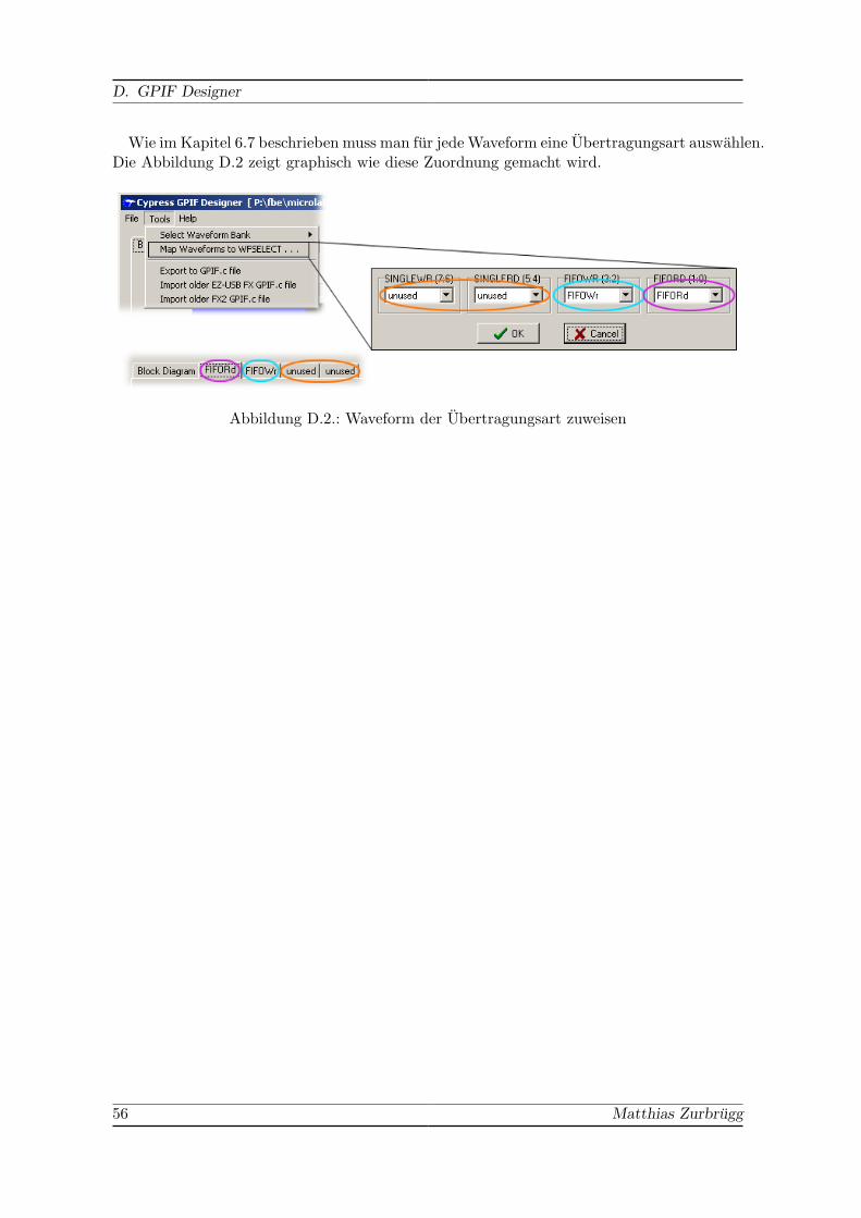
D. GPIF Designer
Wie im Kapitel 6.7 beschrieben muss man fur jede Waveform eine Ubertragungsart auswahlen.Die Abbildung D.2 zeigt graphisch wie diese Zuordnung gemacht wird.
Abbildung D.2.: Waveform der Ubertragungsart zuweisen
56 Matthias Zurbrugg

E. Quellcode
Project Report 57
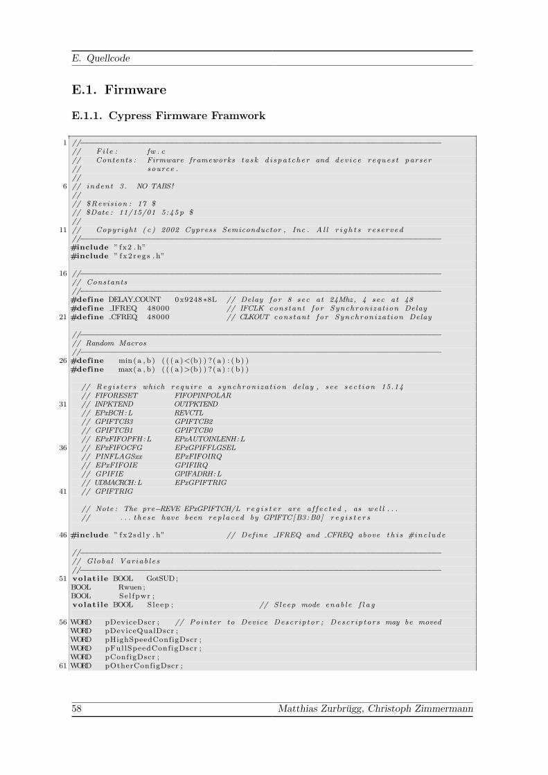
E. Quellcode
E.1. Firmware
E.1.1. Cypress Firmware Framwork
1 //−−−−−−−−−−−−−−−−−−−−−−−−−−−−−−−−−−−−−−−−−−−−−−−−−−−−−−−−−−−−−−−−−−−−−−−−−−−−−// F i l e : fw . c// Contents : Firmware frameworks ta sk d i spa t che r and dev i ce r eque s t parser// source .//
6 // indent 3 . NO TABS!//// $Revis ion : 17 $// $Date : 11/15/01 5:45p $//
11 // Copyright ( c ) 2002 Cypress Semiconductor , Inc . A l l r i g h t s re served//−−−−−−−−−−−−−−−−−−−−−−−−−−−−−−−−−−−−−−−−−−−−−−−−−−−−−−−−−−−−−−−−−−−−−−−−−−−−−#include ” fx2 . h”#include ” f x2 r e g s . h”
16 //−−−−−−−−−−−−−−−−−−−−−−−−−−−−−−−−−−−−−−−−−−−−−−−−−−−−−−−−−−−−−−−−−−−−−−−−−−−−−// Constants//−−−−−−−−−−−−−−−−−−−−−−−−−−−−−−−−−−−−−−−−−−−−−−−−−−−−−−−−−−−−−−−−−−−−−−−−−−−−−#define DELAY COUNT 0x9248∗8L // Delay f o r 8 sec at 24Mhz , 4 sec at 48#define IFREQ 48000 // IFCLK constant f o r Synchronizat ion Delay
21 #define CFREQ 48000 // CLKOUT constant f o r Synchronizat ion Delay
//−−−−−−−−−−−−−−−−−−−−−−−−−−−−−−−−−−−−−−−−−−−−−−−−−−−−−−−−−−−−−−−−−−−−−−−−−−−−−// Random Macros//−−−−−−−−−−−−−−−−−−−−−−−−−−−−−−−−−−−−−−−−−−−−−−−−−−−−−−−−−−−−−−−−−−−−−−−−−−−−−
26 #define min(a , b) ( ( ( a )<(b) ) ?( a ) : ( b ) )#define max(a , b) ( ( ( a )>(b) ) ?( a ) : ( b ) )
// Reg i s t e r s which requ i r e a synchron i za t ion delay , see s e c t i on 15.14// FIFORESET FIFOPINPOLAR
31 // INPKTEND OUTPKTEND// EPxBCH:L REVCTL// GPIFTCB3 GPIFTCB2// GPIFTCB1 GPIFTCB0// EPxFIFOPFH:L EPxAUTOINLENH:L
36 // EPxFIFOCFG EPxGPIFFLGSEL// PINFLAGSxx EPxFIFOIRQ// EPxFIFOIE GPIFIRQ// GPIFIE GPIFADRH:L// UDMACRCH:L EPxGPIFTRIG
41 // GPIFTRIG
// Note : The pre−REVE EPxGPIFTCH/L r e g i s t e r are a f f e c t ed , as we l l . . .// . . . t h e s e have been rep laced by GPIFTC[B3 :B0 ] r e g i s t e r s
46 #include ” fx2 sd l y . h” // Define IFREQ and CFREQ above t h i s #inc lude
//−−−−−−−−−−−−−−−−−−−−−−−−−−−−−−−−−−−−−−−−−−−−−−−−−−−−−−−−−−−−−−−−−−−−−−−−−−−−−// Globa l Var iab l e s//−−−−−−−−−−−−−−−−−−−−−−−−−−−−−−−−−−−−−−−−−−−−−−−−−−−−−−−−−−−−−−−−−−−−−−−−−−−−−
51 volat i le BOOL GotSUD;BOOL Rwuen ;BOOL Sel fpwr ;volat i le BOOL Sleep ; // S leep mode enab le f l a g
56 WORD pDeviceDscr ; // Pointer to Device Descr ip tor ; Descr ip tor s may be movedWORD pDeviceQualDscr ;WORD pHighSpeedConfigDscr ;WORD pFul lSpeedConf igDscr ;WORD pConfigDscr ;
61 WORD pOtherConfigDscr ;
58 Matthias Zurbrugg, Christoph Zimmermann
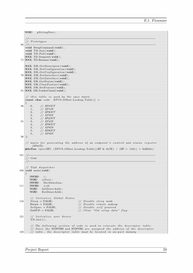
E.1. Firmware
WORD pStr ingDscr ;
//−−−−−−−−−−−−−−−−−−−−−−−−−−−−−−−−−−−−−−−−−−−−−−−−−−−−−−−−−−−−−−−−−−−−−−−−−−−−−// Prototypes
66 //−−−−−−−−−−−−−−−−−−−−−−−−−−−−−−−−−−−−−−−−−−−−−−−−−−−−−−−−−−−−−−−−−−−−−−−−−−−−−void SetupCommand(void ) ;void TD Init (void ) ;void TD Poll (void ) ;BOOL TD Suspend (void ) ;
71 BOOL TD Resume(void ) ;
BOOL DR GetDescriptor (void ) ;BOOL DR SetConfigurat ion (void ) ;BOOL DR GetConfiguration (void ) ;
76 BOOL DR SetInter face (void ) ;BOOL DR GetInterface (void ) ;BOOL DR GetStatus (void ) ;BOOL DR ClearFeature (void ) ;BOOL DR SetFeature (void ) ;
81 BOOL DR VendorCmnd(void ) ;
// t h i s t a b l e i s used by the epcs macroconst char code EPCS Offset Lookup Table [ ] ={
86 0 , // EP1OUT1 , // EP1IN2 , // EP2OUT2 , // EP2IN3 , // EP4OUT
91 3 , // EP4IN4 , // EP6OUT4 , // EP6IN5 , // EP8OUT5 , // EP8IN
96 } ;
// macro fo r genera t ing the address o f an endpoint ’ s con t ro l and s t a t u s r e g i s t e r(EPnCS)
#define epcs (EP) ( EPCS Offset Lookup Table [ (EP & 0x7E) | (EP > 128) ] + 0xE6A1)
101 //−−−−−−−−−−−−−−−−−−−−−−−−−−−−−−−−−−−−−−−−−−−−−−−−−−−−−−−−−−−−−−−−−−−−−−−−−−−−−// Code//−−−−−−−−−−−−−−−−−−−−−−−−−−−−−−−−−−−−−−−−−−−−−−−−−−−−−−−−−−−−−−−−−−−−−−−−−−−−−
// Task d i spa t che r106 void main (void )
{DWORD i ;WORD o f f s e t ;DWORD DevDescrLen ;
111 DWORD j =0;WORD IntDescrAddr ;WORD ExtDescrAddr ;
// I n i t i a l i z e Globa l S ta t e s116 S leep = FALSE; // Disab l e s l e e p mode
Rwuen = FALSE; // Disab l e remote wakeupSe l fpwr = FALSE; // Disab l e s e l f poweredGotSUD = FALSE; // Clear ”Got se tup data” f l a g
121 // I n i t i a l i z e user dev i ceTD Init ( ) ;
// The f o l l ow i n g s e c t i on o f code i s used to r e l o c a t e the d e s c r i p t o r t a b l e .// Since the SUDPTRH and SUDPTRL are ass i gned the address o f the d e s c r i p t o r
126 // tab l e , the d e s c r i p t o r t a b l e must be l o ca t ed in on−part memory .
Project Report 59

E. Quellcode
// The 4K demo t o o l s l o c a t e a l l code s e c t i on s in e x t e rna l memory .// The de s c r i p t o r t a b l e i s r e l o ca t ed by the frameworks ONLY i f i t i s found// to be l o ca t ed in e x t e rna l memory .pDeviceDscr = (WORD)&DeviceDscr ;
131 pDeviceQualDscr = (WORD)&DeviceQualDscr ;pHighSpeedConfigDscr = (WORD)&HighSpeedConfigDscr ;pFul lSpeedConf igDscr = (WORD)&Ful lSpeedConf igDscr ;pStr ingDscr = (WORD)&Str ingDscr ;
136 i f (EZUSB HIGHSPEED() ){
pConfigDscr = pHighSpeedConfigDscr ;pOtherConfigDscr = pFul lSpeedConf igDscr ;
}141 else
{pConfigDscr = pFul lSpeedConf igDscr ;pOtherConfigDscr = pHighSpeedConfigDscr ;
}146
i f ( (WORD)&DeviceDscr & 0xe000 ){
IntDescrAddr = INTERNAL DSCR ADDR;ExtDescrAddr = (WORD)&DeviceDscr ;
151 DevDescrLen = (WORD)&UserDscr − (WORD)&DeviceDscr + 2 ;for ( i = 0 ; i < DevDescrLen ; i++)
∗ ( (BYTE xdata ∗) IntDescrAddr+i ) = 0xCD;for ( i = 0 ; i < DevDescrLen ; i++)
∗ ( (BYTE xdata ∗) IntDescrAddr+i ) = ∗ ( (BYTE xdata ∗) ExtDescrAddr+i ) ;156 pDeviceDscr = IntDescrAddr ;
o f f s e t = (WORD)&DeviceDscr − INTERNAL DSCR ADDR;pDeviceQualDscr −= o f f s e t ;pConfigDscr −= o f f s e t ;pOtherConfigDscr −= o f f s e t ;
161 pHighSpeedConfigDscr −= o f f s e t ;pFul lSpeedConf igDscr −= o f f s e t ;pStr ingDscr −= o f f s e t ;
}
166 EZUSB IRQ ENABLE( ) ; // Enable USB in t e r r up t (INT2)EZUSB ENABLE RSMIRQ( ) ; // Wake−up in t e r r up t
INTSETUP |= (bmAV2EN | bmAV4EN) ; // Enable INT 2 & 4 au tovec to r ing
171 USBIE |= bmSUDAV | bmSUTOK | bmSUSP | bmURES | bmHSGRANT; // Enable s e l e c t e di n t e r r u p t s
EA = 1 ; // Enable 8051 i n t e r r u p t s
#ifndef NORENUM// Renumerate i f necessary . Do t h i s by check ing the renum b i t . I f i t
176 // i s a l ready set , t he re i s no need to renumerate . The renum b i t w i l l// a l ready be s e t i f t h i s firmware was loaded from an eeprom .i f ( ! (USBCS & bmRENUM) ){
EZUSB Discon (TRUE) ; // renumerate181 }
#endif
// uncond i t i ona l l y re−connect . I f we loaded from eeprom we are// disconnec ted and need to connect . I f we j u s t renumerated t h i s
186 // i s not necessary but doesn ’ t hurt anythingUSBCS &= bmDISCON;
CKCON = (CKCON&(˜bmSTRETCH) ) | FW STRETCH VALUE; // Set s t r e t c h to 0 ( a f t e rrenumeration )
60 Matthias Zurbrugg, Christoph Zimmermann
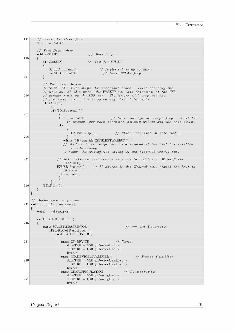
E.1. Firmware
191 // c l e a r the S leep f l a g .Sleep = FALSE;
// Task Dispatcherwhile (TRUE) // Main Loop
196 {i f (GotSUD) // Wait f o r SUDAV{
SetupCommand ( ) ; // Implement se tup commandGotSUD = FALSE; // Clear SUDAV f l a g
201 }
// Po l l User Device// NOTE: I d l e mode s tops the processor c l o c k . There are only two// ways out o f i d l e mode , the WAKEUP pin , and de t e c t i on o f the USB
206 // resume s t a t e on the USB bus . The t imers w i l l s top and the// processor w i l l not wake up on any other i n t e r r u p t s .i f ( S leep )
{i f (TD Suspend ( ) )
211 {Sleep = FALSE; // Clear the ”go to s l e e p ” f l a g . Do i t here
to prevent any race cond i t i on between wakeup and the next s l e e p .do
{EZUSB Susp ( ) ; // Place processor in i d l e mode .
216 }while ( ! Rwuen && EZUSB EXTWAKEUP( ) ) ;// Must cont inue to go back in to suspend i f the hos t has d i s a b l e d
remote wakeup// ∗and∗ the wakeup was caused by the e x t e rna l wakeup pin .
221 // 8051 a c t i v i t y w i l l resume here due to USB bus or Wakeup# pina c t i v i t y .
EZUSB Resume ( ) ; // I f source i s the Wakeup# pin , s i g n a l the hos t toResume .
TD Resume ( ) ;}
}226 TD Poll ( ) ;
}}
// Device reque s t parser231 void SetupCommand(void )
{void ∗ d s c r p t r ;
switch (SETUPDAT[ 1 ] )236 {
case SC GET DESCRIPTOR: // ∗∗∗ Get Descr ip tori f ( DR GetDescriptor ( ) )
switch (SETUPDAT[ 3 ] ){
241 case GD DEVICE: // DeviceSUDPTRH = MSB( pDeviceDscr ) ;SUDPTRL = LSB( pDeviceDscr ) ;break ;
case GD DEVICE QUALIFIER: // Device Qua l i f i e r246 SUDPTRH = MSB( pDeviceQualDscr ) ;
SUDPTRL = LSB( pDeviceQualDscr ) ;break ;
case GD CONFIGURATION: // Conf igurat ionSUDPTRH = MSB( pConfigDscr ) ;
251 SUDPTRL = LSB( pConfigDscr ) ;break ;
Project Report 61
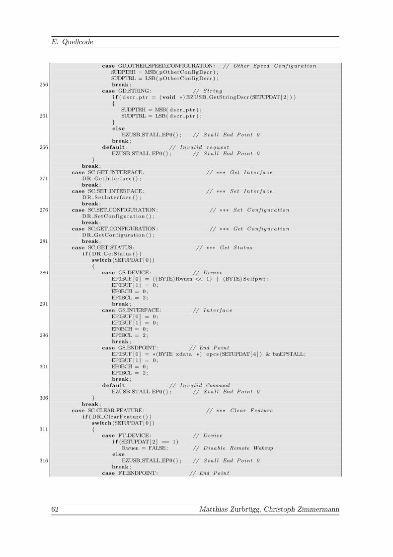
E. Quellcode
case GD OTHER SPEED CONFIGURATION: // Other Speed Conf igurat ionSUDPTRH = MSB( pOtherConfigDscr ) ;SUDPTRL = LSB( pOtherConfigDscr ) ;
256 break ;case GD STRING: // S t r ing
i f ( d s c r p t r = (void ∗) EZUSB GetStringDscr (SETUPDAT[ 2 ] ) ){
SUDPTRH = MSB( d s c r p t r ) ;261 SUDPTRL = LSB( d s c r p t r ) ;
}else
EZUSB STALL EP0( ) ; // S t a l l End Point 0break ;
266 default : // In va l i d r eque s tEZUSB STALL EP0( ) ; // S t a l l End Point 0
}break ;
case SC GET INTERFACE: // ∗∗∗ Get In t e r f a c e271 DR GetInterface ( ) ;
break ;case SC SET INTERFACE: // ∗∗∗ Set In t e r f a c e
DR SetInter face ( ) ;break ;
276 case SC SET CONFIGURATION: // ∗∗∗ Set Conf igurat ionDR SetConfigurat ion ( ) ;break ;
case SC GET CONFIGURATION: // ∗∗∗ Get Conf igurat ionDR GetConfiguration ( ) ;
281 break ;case SC GET STATUS: // ∗∗∗ Get Sta tus
i f ( DR GetStatus ( ) )switch (SETUPDAT[ 0 ] ){
286 case GS DEVICE: // DeviceEP0BUF[ 0 ] = ( (BYTE)Rwuen << 1) | (BYTE) Se l fpwr ;EP0BUF[ 1 ] = 0 ;EP0BCH = 0 ;EP0BCL = 2 ;
291 break ;case GS INTERFACE: // In t e r f a c e
EP0BUF[ 0 ] = 0 ;EP0BUF[ 1 ] = 0 ;EP0BCH = 0 ;
296 EP0BCL = 2 ;break ;
case GS ENDPOINT: // End PointEP0BUF[ 0 ] = ∗(BYTE xdata ∗) epcs (SETUPDAT[ 4 ] ) & bmEPSTALL;EP0BUF[ 1 ] = 0 ;
301 EP0BCH = 0 ;EP0BCL = 2 ;break ;
default : // In va l i d CommandEZUSB STALL EP0( ) ; // S t a l l End Point 0
306 }break ;
case SC CLEAR FEATURE: // ∗∗∗ Clear Featurei f ( DR ClearFeature ( ) )
switch (SETUPDAT[ 0 ] )311 {
case FT DEVICE: // Devicei f (SETUPDAT[ 2 ] == 1)
Rwuen = FALSE; // Disab l e Remote Wakeupelse
316 EZUSB STALL EP0( ) ; // S t a l l End Point 0break ;
case FT ENDPOINT: // End Point
62 Matthias Zurbrugg, Christoph Zimmermann

E.1. Firmware
i f (SETUPDAT[ 2 ] == 0){
321 ∗(BYTE xdata ∗) epcs (SETUPDAT[ 4 ] ) &= ˜bmEPSTALL;EZUSB RESET DATA TOGGLE( SETUPDAT[ 4 ] ) ;
}else
EZUSB STALL EP0( ) ; // S t a l l End Point 0326 break ;
}break ;
case SC SET FEATURE: // ∗∗∗ Set Featurei f ( DR SetFeature ( ) )
331 switch (SETUPDAT[ 0 ] ){
case FT DEVICE: // Devicei f (SETUPDAT[ 2 ] == 1)
Rwuen = TRUE; // Enable Remote Wakeup336 else i f (SETUPDAT[ 2 ] == 2)
// Set Feature Test Mode . The core hand les t h i s r e que s t .However , i t i s
// necessary f o r the firmware to complete the handshake phase o fthe
// con t ro l t r an s f e r be f o r e the chip w i l l en ter t e s t mode . I t i sa l s o
// necessary f o r FX2 to be p h y s i c a l l y d i sconnected (D+ and D−)341 // from the hos t b e f o r e i t w i l l en ter t e s t mode .
break ;else
EZUSB STALL EP0( ) ; // S t a l l End Point 0break ;
346 case FT ENDPOINT: // End Point∗(BYTE xdata ∗) epcs (SETUPDAT[ 4 ] ) |= bmEPSTALL;break ;
}break ;
351 default : // ∗∗∗ I n va l i d Commandi f (DR VendorCmnd( ) )
EZUSB STALL EP0( ) ; // S t a l l End Point 0}
356 // Acknowledge handshake phase o f dev i ce r eque s tEP0CS |= bmHSNAK;
}
// Wake−up in t e r r up t handler361 void r e sume i s r (void ) i n t e r r up t WKUPVECT
{EZUSB CLEAR RSMIRQ( ) ;
}
E.1.2. Firmware
1 #pragma NOIV // Do not generate i n t e r r up t v e c t o r s/∗ ∗∗∗∗∗∗∗∗∗∗∗∗∗∗∗∗∗∗∗∗∗∗∗∗∗∗∗∗∗∗∗∗∗∗∗∗∗∗∗∗∗∗∗∗∗∗∗∗∗∗∗∗∗∗∗∗∗∗∗ Diplomwork :∗ Gecko3 SoC HW/SW Development Board∗
6 ∗ ( ‘\ ( ) ( ) ( )∗ | ( ) ) | ( | | | | Berne Unive r s i t y o f Appl ied Sciences∗ | < ’| ) | | School o f Engineering and∗ | ( ) ) | | | | | | Information Technology∗ ( / ’( ) ( ) ( )
11 ∗∗
Project Report 63

E. Quellcode
∗ Author : Matthias Zurbrugg∗ Date o f c rea t i on : 22.11.2006∗ Descr ip t ion :
16 ∗ Source code o f Cypress EZ−USB FX2 Firmware∗∗∗∗∗∗∗∗∗∗∗∗∗∗∗∗∗∗∗∗∗∗∗∗∗∗∗∗∗∗∗∗∗∗∗∗∗∗∗∗∗∗∗∗∗∗∗∗∗∗∗∗∗∗∗∗∗∗∗ ∗/
#include ” fx2 . h”21 #include ” f x2 r e g s . h”
#include ” fx2 sd l y . h” // SYNCDELAY macro , see Sect ion 15.14 o f FX2 Tech .// Ref . Manual f o r usage d e t a i l s .
#include ” gp i f r d w r f un c . h”#include ” s p i f l a s h r d w r f u n c . h”
26 #include ” f p g a c f g f un c . h”#include ” eeprom rd wr func . h”
// firmware vers ion (max three d i g i t s )#define f w v e r d i g i t 0 ’ 1 ’
31 #define f w v e r d i g i t 1 ’ . ’#define f w v e r d i g i t 2 ’ 0 ’#define f w v e r d i g i t 3 ’ 1 ’
// Cypres b i t masks36 #define bmEP0BSY 0x01
#define bmEP1OUTBSY 0x02#define bmEP1INBSY 0x04
// Def ines f o r EEPROM communications41 #define wri te nok 1
#define wr i t e ok 0#define read nok 1#define read ok 0#define i n i t 0
46 #define i d l e 3
// Cypres v a r i a b l e sextern BOOL GotSUD; // Received se tup data f l a gextern BOOL Sleep ;
51 extern BOOL Rwuen ;extern BOOL Sel fpwr ;
BYTE Conf igurat ion ; // Current con f i gu ra t i onBYTE Al t e rna t eSe t t i ng ; // Al terna te s e t t i n g s
56// Var iab l e s f o r GPIF communicationsBOOL in enab l e = FALSE; // f l a g to enab le IN t r an s f e r sBOOL f i f o r d e n a b l e = FALSE; // f l a g to enab le GPIF FIFO READ TransactionBOOL f i f o r d i n t = FALSE; // GPIF FIFO READ Transaction i n t e r r up t f l a g
61 BOOL enum high speed = FALSE; // f l a g to l e t firmware know FX2 enumerated ath igh speed
// Var iab l e s f o r EEPROM coummunicationsBOOL eeprom write mode = FALSE; // s e t eeprome write mode to f a l s eBOOL s t a r t t r a n s a c t i o n = 1 ;BOOL eeprom read mode = FALSE;
66 BYTE eeprom read s ta te = i d l e ; // s e t eeprom read s t a t e on i d l eWORD eeprom adress = 0 ;WORD read count = 0 ; // va lue o f number o f by t e s to read// Var iab l e s f o r FPGA con f i gu ra t i onBOOL fpga cfg mode = FALSE; // FPGA con f i gu ra t i on mode v a r i a b l e
71 BOOL done ack = FALSE; // v a r i a b l e to g i v e vendor reque s t DONEacknoledgement
// Var iab l e s f o r SPI Flash communicationsBOOL sp i f l a s h wr i t e mode = FALSE;BOOL sp i f l a sh r e ad mode = FALSE;BOOL f l a s h r d e n ;
76 BOOL new cfg = 1 ;
64 Matthias Zurbrugg, Christoph Zimmermann

E.1. Firmware
unsigned long s p i f l a s h a d r e s s =0;
//−−−−−−−−−−−−−−−−−−−−−−−−−−−−−−−−−−−−−−−−−−−−−−−−−−−−−−−−−−−−−−−−−−−−−−−−−−−−−// Task Dispatcher hooks
81 // The f o l l ow i n g hooks are c a l l e d by the ta sk d i s pa t che r .//−−−−−−−−−−−−−−−−−−−−−−−−−−−−−−−−−−−−−−−−−−−−−−−−−−−−−−−−−−−−−−−−−−−−−−−−−−−−−void Gp i f I n i t (void ) ; // func t ion pro to type from gp i f . c
void TD Init (void ) // Cal l ed once at s t a r t up86 {
// s e t the CPU c lock to 48MHzCPUCS = ((CPUCS & ˜bmCLKSPD) | bmCLKSPD1) ;SYNCDELAY;
91 EP1OUTCFG = 0xA0 ; // always OUT, va l i d , bu l kEP1INCFG = 0xA0 ; // always IN , va l i d , bu l kSYNCDELAY;EP2CFG = 0xA2 ; // EP2OUT, bulk , s i z e 512 , 2x bu f f e r e dSYNCDELAY;
96 EP4CFG = 0xE0 ; // EP4IN, bulk , s i z e 512 , 2x bu f f e r e dSYNCDELAY;EP6CFG = 0xA2 ; // EP6OUT, bulk , s i z e 512 , 2x bu f f e r e dSYNCDELAY;EP8CFG = 0xE0 ; // EP8IN, bulk , s i z e 512 , 2x bu f f e r e d
101 SYNCDELAY;
// out endpoints do not come up armed// s ince the d e f a u l t s are doub le bu f f e r e d we must wr i t e dummy by te counts tw iceSYNCDELAY;
106 EP2BCL = 0x80 ; // arm EP2OUT by wr i t i n g by te count w/ sk i p .SYNCDELAY;EP2BCL = 0x80 ;SYNCDELAY;
111 FIFORESET = 0x80 ; // s e t NAKALL b i t to NAK a l l t r an s f e r s from hos t/∗SYNCDELAY;FIFORESET = 0x02 ; // r e s e t EP2 FIFOSYNCDELAY;FIFORESET = 0x04 ; // r e s e t EP4 FIFO
116 SYNCDELAY; ∗/FIFORESET = 0x06 ; // r e s e t EP6 FIFOSYNCDELAY;FIFORESET = 0x08 ; // r e s e t EP8 FIFOSYNCDELAY;
121 FIFORESET = 0x00 ; // c l e a r NAKALL b i t to resume normal opera t ionSYNCDELAY;
EP6FIFOCFG = 0x00 ; // a l l ow core to see zero to one t r an s i t i o n o f auto out b i tSYNCDELAY;
126 EP6FIFOCFG = 0x10 ; // auto out mode , d i s a b l e PKTEND zero l eng t h send , by te opsSYNCDELAY;EP8FIFOCFG = 0x08 ; // auto in mode , d i s a b l e PKTEND zero l eng t h send , by te opsSYNCDELAY;EP1OUTBC = 0x00 ; // arm EP1OUT by wr i t i n g any va lue to EP1OUTBC r e g i s t e r
131s p i f l a s h i n i t ( ) ; // i n i t i a l i z e Port A [ 0 : 3 ] ( func t i on in s p i f l a s h r d w r f u n c . c )f p g a c f g i n i t ( ) ; // i n i t i a l i z e Port A [ 4 : 7 ] , Port B and CTL0 fo r FPGA
con f i gu ra t i on ( func t i on in f p g a c f g f un c . c )boo t l oad c f g ( ) ; // s t a r t l oad ing FPGA con f i gu ra t i on from SPI Flash in FPGA
( func t ion in s p i f l a s h r d w r f u n c . c )
136 Gp i f I n i t ( ) ; // i n i t i a l i z e GPIF r e g i s t e r s ( func t i on in g p i f . c )
EZUSB InitI2C ( ) ;
//PORTACFG = bmINT0; // PA0 take s on INT0/ a l t e r n a t e func t i on
Project Report 65

E. Quellcode
141 //OEA |= 0x0C ; // i n i t i a l i z e PA3 and PA2 port i /o pins as output s//PORTECFG = 0x07 ;
}
void TD Poll (void ) // c a l l e d r epea t ed l y wh i l e the dev i ce i s i d l e146 {
i f ( ! ( EP2468STAT & bmEP2EMPTY ) ) // i f t he re ’ s a packet in the pe r i ph e ra ldomain fo r EP2
{i f ( fpga c fg mode == TRUE) // vendor command 0xC1 fo r FPGA con f i gu ra t i on
mode{
151 f p g a c f g i n i t ( ) ; // i n i t a l i z e i /o l i n e s f o r FPGA con f i gu ra t i on mode( func t i on in f p g a c f g f un c . c )
f p g a c f g ( ) ; // c a l l FPGA con f i gu ra t i on prozedure ( func t i on inf p g a c f g f un c . c )
}
i f ( eeprom write mode == TRUE) // vendor command 0xC2 load firmware in EEPROM156 {
eeprom wr ( ) ; // c a l l EEPROM wri t e}
i f ( s p i f l a s h wr i t e mode == TRUE) // vendor command 0xC4 load FPGAcon f i gu ra t i on in SPI Flash , va lue in EP0 i s con f i gu ra t i on part (0 or 1)−−−−>> to do
161 {s p i f l a s h w r ( ) ; // c a l l SPI Flash wr i t e
}}
166 i f ( eeprom read mode == TRUE) // vendor command 0xC3 read firmware fromEEPROM, va lue in EP0 i s number o f by t e s to read
{eeprom rd ( read count ) ; // c a l l EEPROM read
}
171 i f ( s p i f l a sh r e ad mode == TRUE) // vendor command 0xC5 read FPGAcon f i gu ra t i on from SPI Flash , va lue in EP0 i s number o f by t e s to read
{s p i f l a s h r d ( ) ; // c a l l SPI Flash read
}
176 i f ( ! ( EP2468STAT & bmEP6EMPTY ) ) // i f t he re ’ s a packet in the pe r i ph e ra ldomain fo r EP6
{gpi f wr waveform ( ) ; // c a l l f unc t i on to s t a r t a GPIF FIFO WRITE
Transaction ( func t i on in gp i f r d wr f un c . c )i n enab l e = TRUE;}
181 i f ( i n enab l e ) { // s t a r t communicationgp i f rd wave form ( ) ; // c a l l f unc t i on to s t a r t a GPIF FIFO READ
Transaction ( func t i on in gp i f r d wr f un c . c )}
186 i f ( ! (EP01STAT & bmEP1OUTBSY) ){
// handle OUTs to EP1OUT}
191 i f ( ! (EP01STAT & bmEP1INBSY) ){
// handle INs to EP1IN}
}
66 Matthias Zurbrugg, Christoph Zimmermann

E.1. Firmware
196BOOL TD Suspend (void ) // Cal l ed be f o r e the dev i ce goes in to suspend mode{
return (TRUE) ;}
201BOOL TD Resume(void ) // Cal l ed a f t e r the dev i ce resumes{
return (TRUE) ;}
206//−−−−−−−−−−−−−−−−−−−−−−−−−−−−−−−−−−−−−−−−−−−−−−−−−−−−−−−−−−−−−−−−−−−−−−−−−−−−−// Device Request hooks// The f o l l ow i n g hooks are c a l l e d by the end po in t 0 dev i ce r eque s t parser .//−−−−−−−−−−−−−−−−−−−−−−−−−−−−−−−−−−−−−−−−−−−−−−−−−−−−−−−−−−−−−−−−−−−−−−−−−−−−−
211BOOL DR GetDescriptor (void ){
return (TRUE) ;}
216BOOL DR SetConfigurat ion (void ) // Cal l ed when a Set Conf igurat ion command i s
r ece i v ed{
i f ( EZUSB HIGHSPEED( ) )221 { // FX2 enumerated at h igh speed
SYNCDELAY;EP6AUTOINLENH = 0x02 ; // s e t AUTOIN commit l eng t h to 512 by t e sSYNCDELAY;EP6AUTOINLENL = 0x00 ;
226 SYNCDELAY;enum high speed = TRUE;
}else{ // FX2 enumerated at f u l l speed
231 SYNCDELAY;EP6AUTOINLENH = 0x00 ; // s e t AUTOIN commit l eng t h to 64 by t e sSYNCDELAY;EP6AUTOINLENL = 0x40 ;SYNCDELAY;
236 enum high speed = FALSE;}
Conf igurat ion = SETUPDAT[ 2 ] ;return (TRUE) ; // Handled by user code
241 }
BOOL DR GetConfiguration (void ) // Cal l ed when a Get Conf igurat ion command i sr ece i v ed
{EP0BUF[ 0 ] = Conf igurat ion ;
246 EP0BCH = 0 ;EP0BCL = 1 ;return (TRUE) ; // Handled by user code
}
251 BOOL DR SetInter face (void ) // Cal l ed when a Set I n t e r f a c e command i s r ece i v ed{
Al t e rna t eSe t t i ng = SETUPDAT[ 2 ] ;return (TRUE) ; // Handled by user code
}256
BOOL DR GetInterface (void ) // Cal l ed when a Get In t e r f a c e command i s r ece i v ed{
EP0BUF[ 0 ] = Al t e rna t eSe t t i ng ;
Project Report 67

E. Quellcode
EP0BCH = 0 ;261 EP0BCL = 1 ;
return (TRUE) ; // Handled by user code}
BOOL DR GetStatus (void )266 {
return (TRUE) ;}
BOOL DR ClearFeature (void )271 {
return (TRUE) ;}
BOOL DR SetFeature (void )276 {
return (TRUE) ;}
#define FPGA CFG 0xC1 // vendor reque s t f o r FPGA con f i gu ra t i on mode281 #define EEPROM WRITE 0xC2 // vendor reque s t load firmware in EEPROM
#define EEPROM READ 0xC3 // vendor reque s t read firmware from EEPROM, va lue inEP0 i s number o f by t e s to read
#define FLASH WRITE 0xC4 // vendor reque s t load FPGA con f i gu ra t i on in SPI Flash ,va lue in EP0 i s con f i gu ra t i on part (0 or 1) −−−−>> to do
#define FLASH READ 0xC5 // vendor reque s t read FPGA con f i gu ra t i on from SPIFlash
#define DOWNLOADOK 0xC6 // vendor reque s t f o r complete data t r an s f e r286 //#de f ine GPIF READ 0xC9 // enab le IN t r an s f e r s f o r GPIF communication
#define FW VERSION 0xB1 // ge t firmware vers ion#define DONE REQ 0xB2 // ge t DONE b i t from FPGA
BOOL DR VendorCmnd(void )291 {
switch (SETUPDAT[ 1 ] ){case FPGA CFG:{
296 fpga c fg mode = TRUE; // s e t FPGA con f i gu ra t i on mode∗EP0BUF = FPGA CFG; // loopback from vendor command
EP0BCH = 0 ;EP0BCL = 1 ; // Arm endpoint with # by t e s to t r an s f e rEP0CS |= bmHSNAK; // Acknowledge handshake phase o f dev i ce r eque s t
301 break ;}case EEPROM WRITE:{
eeprom write mode = TRUE; // s e t EEPROME wri t e mode306 ∗EP0BUF = EEPROM WRITE; // loopback from vendor command
EP0BCH = 0 ;EP0BCL = 1 ; // Arm endpoint with # by t e s to t r an s f e rEP0CS |= bmHSNAK; // Acknowledge handshake phase o f dev i ce r eque s tbreak ;
311 }case EEPROM READ:{
eeprom read s ta te = i n i t ; // s e t i n i t i a t i o n s t a t eEP0BCL = 0 ; // re−arm EP0
316 while (EP01STAT & bmEP0BSY) ; // wait u n t i l EP0 i s a v a i l a b l e to beaccessed by CPU
read count = EP0BUF [ 0 ] ; // read high by te number o f by t e s to readread count = ( read count << 8) | EP0BUF [ 1 ] ; // read low by te number o f by t e s to
read/∗EP0BCL = 1; // Arm endpoint with # by t e s to t r an s f e r
68 Matthias Zurbrugg, Christoph Zimmermann

E.1. Firmware
EP0CS |= bmHSNAK; ∗/ // Acknowledge handshake phase o f dev i cer eque s t
321 break ;}case FLASH WRITE:{
s p i f l a s h wr i t e mode = TRUE; // s e t EEPROME wri t e mode326 ∗EP0BUF = EEPROM READ; // loopback from vendor command
EP0BCH = 0 ;EP0BCL = 1 ; // Arm endpoint with # by t e s to t r an s f e rEP0CS |= bmHSNAK; // Acknowledge handshake phase o f dev i ce r eque s tbreak ;
331 }case FLASH READ:{
sp i f l a sh r e ad mode = TRUE; // s e t EEPROME wri t e mode∗EP0BUF = EEPROM READ; // loopback from vendor command
336 EP0BCH = 0 ;EP0BCL = 1 ; // Arm endpoint with # by t e s to t r an s f e rEP0CS |= bmHSNAK; // Acknowledge handshake phase o f dev i ce r eque s tbreak ;
}341 case DOWNLOADOK:
{// SPI Flash d e f a u l t con f i g
new cfg = 1 ;s p i f l a s h a d r e s s = 0 ;
346 // EEPROM de f a u l t con f i geeprom adress = 0 ; // c l e a r adress va lueeeprom write mode = FALSE;
∗EP0BUF = DOWNLOADOK; // loopback from vendor command351 EP0BCH = 0 ;
EP0BCL = 1 ; // Arm endpoint with # by t e s to t r an s f e rEP0CS |= bmHSNAK; // Acknowledge handshake phase o f dev i ce r eque s tbreak ;
}356 case FW VERSION:
{EP0BUF[ 0 ] = fw v e r d i g i t 0 ; // loopback from vendor command
EP0BUF[ 1 ] = fw v e r d i g i t 1 ;EP0BUF[ 2 ] = fw v e r d i g i t 2 ;
361 EP0BUF[ 3 ] = fw v e r d i g i t 3 ;EP0BCH = 0 ;
EP0BCL = 4 ; // Arm endpoint with # by t e s to t r an s f e rEP0CS |= bmHSNAK; // Acknowledge handshake phase o f dev i ce r eque s tbreak ;
366 }case DONE REQ:{
i f ( done ack == TRUE){
371 done ack = FALSE;∗EP0BUF = DONE REQ;
} else{
∗EP0BUF = 0 ;376 }
EP0BCH = 0 ;EP0BCL = 1 ;EP0CS |= bmHSNAK;
break ;381 }
default :return (TRUE) ;
}
Project Report 69
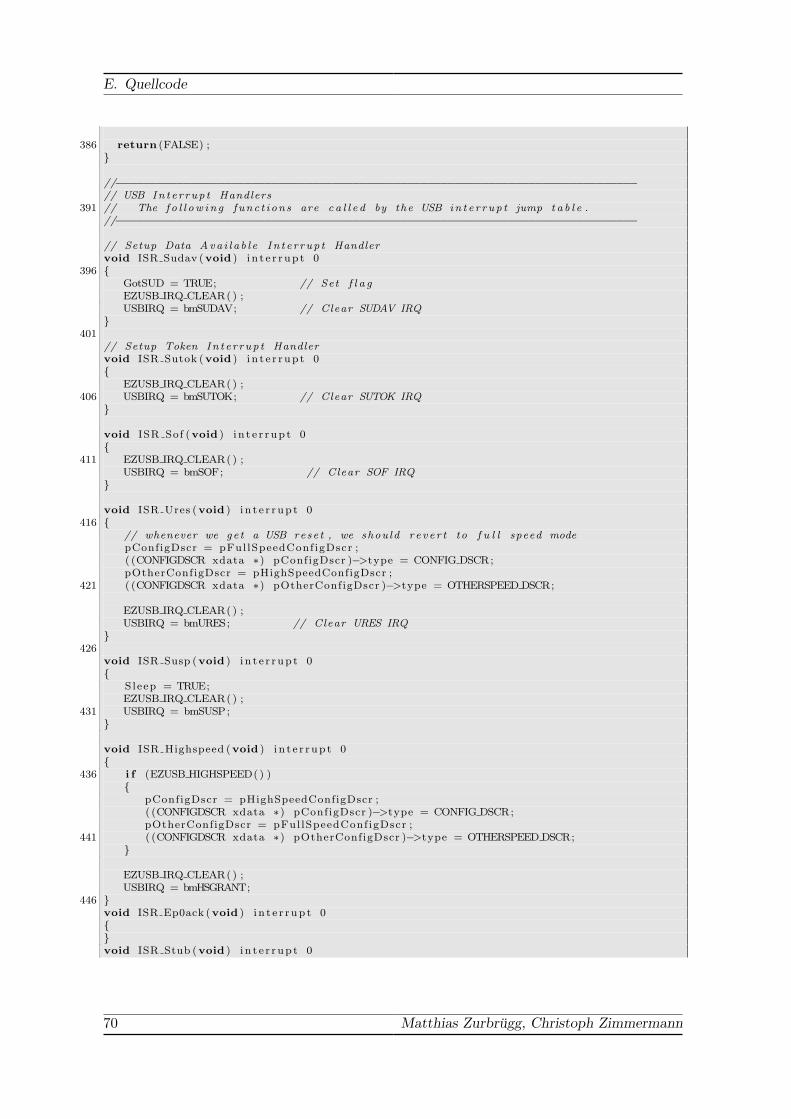
E. Quellcode
386 return (FALSE) ;}
//−−−−−−−−−−−−−−−−−−−−−−−−−−−−−−−−−−−−−−−−−−−−−−−−−−−−−−−−−−−−−−−−−−−−−−−−−−−−−// USB In t e r rup t Handlers
391 // The f o l l ow i n g func t i on s are c a l l e d by the USB in t e r r up t jump t a b l e .//−−−−−−−−−−−−−−−−−−−−−−−−−−−−−−−−−−−−−−−−−−−−−−−−−−−−−−−−−−−−−−−−−−−−−−−−−−−−−
// Setup Data Ava i l a b l e In t e r rup t Handlervoid ISR Sudav (void ) i n t e r r up t 0
396 {GotSUD = TRUE; // Set f l a gEZUSB IRQ CLEAR() ;USBIRQ = bmSUDAV; // Clear SUDAV IRQ
}401
// Setup Token In t e r rup t Handlervoid ISR Sutok (void ) i n t e r r up t 0{
EZUSB IRQ CLEAR() ;406 USBIRQ = bmSUTOK; // Clear SUTOK IRQ
}
void ISR Sof (void ) i n t e r r up t 0{
411 EZUSB IRQ CLEAR() ;USBIRQ = bmSOF; // Clear SOF IRQ
}
void ISR Ures (void ) i n t e r r up t 0416 {
// whenever we ge t a USB rese t , we shou ld r e v e r t to f u l l speed modepConfigDscr = pFul lSpeedConf igDscr ;( (CONFIGDSCR xdata ∗) pConfigDscr )−>type = CONFIG DSCR;pOtherConfigDscr = pHighSpeedConfigDscr ;
421 ( (CONFIGDSCR xdata ∗) pOtherConfigDscr )−>type = OTHERSPEED DSCR;
EZUSB IRQ CLEAR() ;USBIRQ = bmURES; // Clear URES IRQ
}426
void ISR Susp (void ) i n t e r r up t 0{
Sleep = TRUE;EZUSB IRQ CLEAR() ;
431 USBIRQ = bmSUSP;}
void ISR Highspeed (void ) i n t e r r up t 0{
436 i f (EZUSB HIGHSPEED() ){
pConfigDscr = pHighSpeedConfigDscr ;( (CONFIGDSCR xdata ∗) pConfigDscr )−>type = CONFIG DSCR;pOtherConfigDscr = pFul lSpeedConf igDscr ;
441 ( (CONFIGDSCR xdata ∗) pOtherConfigDscr )−>type = OTHERSPEED DSCR;}
EZUSB IRQ CLEAR() ;USBIRQ = bmHSGRANT;
446 }void ISR Ep0ack (void ) i n t e r r up t 0{}void ISR Stub (void ) i n t e r r up t 0
70 Matthias Zurbrugg, Christoph Zimmermann

E.1. Firmware
451 {}void ISR Ep0in (void ) i n t e r r up t 0{}
456 void ISR Ep0out (void ) i n t e r r up t 0{}void ISR Ep1in (void ) i n t e r r up t 0{
461 }void ISR Ep1out (void ) i n t e r r up t 0{}void ISR Ep2inout (void ) i n t e r r up t 0
466 {}void ISR Ep4inout (void ) i n t e r r up t 0{}
471 void ISR Ep6inout (void ) i n t e r r up t 0{}void ISR Ep8inout (void ) i n t e r r up t 0{
476 }void ISR Ibn (void ) i n t e r r up t 0{}void ISR Ep0pingnak (void ) i n t e r r up t 0
481 {}void ISR Ep1pingnak (void ) i n t e r r up t 0{}
486 void ISR Ep2pingnak (void ) i n t e r r up t 0{}void ISR Ep4pingnak (void ) i n t e r r up t 0{
491 }void ISR Ep6pingnak (void ) i n t e r r up t 0{}void ISR Ep8pingnak (void ) i n t e r r up t 0
496 {}void ISR Erro r l im i t (void ) i n t e r r up t 0{}
501 void ISR Ep2piderror (void ) i n t e r r up t 0{}void ISR Ep4piderror (void ) i n t e r r up t 0{
506 }void ISR Ep6piderror (void ) i n t e r r up t 0{}void ISR Ep8piderror (void ) i n t e r r up t 0
511 {}void ISR Ep2pflag (void ) i n t e r r up t 0{}
516 void ISR Ep4pflag (void ) i n t e r r up t 0
Project Report 71

E. Quellcode
{}void ISR Ep6pflag (void ) i n t e r r up t 0{
521 }void ISR Ep8pflag (void ) i n t e r r up t 0{}void ISR Ep2ef lag (void ) i n t e r r up t 0
526 {}void ISR Ep4ef lag (void ) i n t e r r up t 0{}
531 void ISR Ep6ef lag (void ) i n t e r r up t 0{}void ISR Ep8ef lag (void ) i n t e r r up t 0{
536 }void ISR Ep2f f lag (void ) i n t e r r up t 0{}void ISR Ep4f f lag (void ) i n t e r r up t 0
541 {}void ISR Ep6f f lag (void ) i n t e r r up t 0{}
546 void ISR Ep8f f lag (void ) i n t e r r up t 0{}void ISR GpifComplete (void ) i n t e r r up t 0{
551 }void ISR GpifWaveform (void ) i n t e r r up t 0{}
E.1.3. FPGA Konfiguration
/∗ ∗∗∗∗∗∗∗∗∗∗∗∗∗∗∗∗∗∗∗∗∗∗∗∗∗∗∗∗∗∗∗∗∗∗∗∗∗∗∗∗∗∗∗∗∗∗∗∗∗∗∗∗∗∗∗∗∗∗∗ Diplomwork :∗ Gecko3 SoC HW/SW Development Board∗
5 ∗ ( ‘\ ( ) ( ) ( )∗ | ( ) ) | ( | | | | Berne Unive r s i t y o f Appl ied Sciences∗ | < ’| ) | | School o f Engineering and∗ | ( ) ) | | | | | | Information Technology∗ ( / ’( ) ( ) ( )
10 ∗∗∗ Author : Matthias Zurbrugg∗ Date o f c rea t i on : 31.10.2006∗ Descr ip t ion :
15 ∗ Source code FPGA con f i gu ra t i on from Host over USB∗∗∗∗∗∗∗∗∗∗∗∗∗∗∗∗∗∗∗∗∗∗∗∗∗∗∗∗∗∗∗∗∗∗∗∗∗∗∗∗∗∗∗∗∗∗∗∗∗∗∗∗∗∗∗∗∗∗∗ ∗/
#include ” fx2 . h”20 #include ” f x2 r e g s . h”
#include ” fx2 sd l y . h” // SYNCDELAY macro
72 Matthias Zurbrugg, Christoph Zimmermann
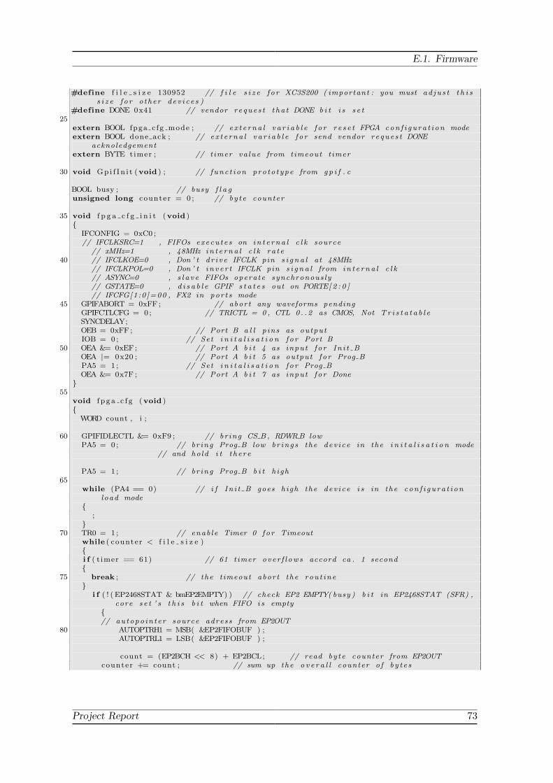
E.1. Firmware
#define f i l e s i z e 130952 // f i l e s i z e f o r XC3S200 ( important : you must ad ju s t t h i ss i z e f o r o ther dev i c e s )
#define DONE 0x41 // vendor reque s t t ha t DONE b i t i s s e t25
extern BOOL fpga cfg mode ; // e x t e rna l v a r i a b l e f o r r e s e t FPGA con f i gu ra t i on modeextern BOOL done ack ; // e x t e rna l v a r i a b l e f o r send vendor reque s t DONE
acknoledgementextern BYTE timer ; // timer va lue from timeout t imer
30 void Gp i f I n i t (void ) ; // func t ion pro to type from gp i f . c
BOOL busy ; // busy f l a gunsigned long counter = 0 ; // by te counter
35 void f p g a c f g i n i t (void ){
IFCONFIG = 0xC0 ;// IFCLKSRC=1 , FIFOs execu te s on i n t e r na l c l k source
// xMHz=1 , 48MHz in t e r na l c l k ra t e40 // IFCLKOE=0 , Don ’ t d r i v e IFCLK pin s i g n a l at 48MHz
// IFCLKPOL=0 , Don ’ t i n v e r t IFCLK pin s i g n a l from in t e rna l c l k// ASYNC=0 , s l a v e FIFOs operate synchronous ly// GSTATE=0 , d i s a b l e GPIF s t a t e s out on PORTE[ 2 : 0 ]// IFCFG[1:0 ]=00 , FX2 in por t s mode
45 GPIFABORT = 0xFF ; // abor t any waveforms pendingGPIFCTLCFG = 0 ; // TRICTL = 0 , CTL 0 . . 2 as CMOS, Not T r i s t a t a b l eSYNCDELAY;OEB = 0xFF ; // Port B a l l p ins as outputIOB = 0 ; // Set i n i t a l i s a t i o n fo r Port B
50 OEA &= 0xEF ; // Port A b i t 4 as input f o r In i t BOEA |= 0x20 ; // Port A b i t 5 as output f o r Prog BPA5 = 1 ; // Set i n i t a l i s a t i o n fo r Prog BOEA &= 0x7F ; // Port A b i t 7 as input f o r Done
}55
void f p g a c f g (void ){
WORD count , i ;
60 GPIFIDLECTL &= 0xF9 ; // br ing CS B , RDWRB lowPA5 = 0 ; // br ing Prog B low br ing s the dev i ce in the i n i t a l i s a t i o n mode
// and ho ld i t t he re
PA5 = 1 ; // br ing Prog B b i t h igh65
while (PA4 == 0) // i f In i t B goes high the dev i ce i s in the con f i gu ra t i onload mode
{;
}70 TR0 = 1 ; // enab le Timer 0 fo r Timeout
while ( counter < f i l e s i z e ){i f ( t imer == 61) // 61 timer ove r f l ows accord ca . 1 second{
75 break ; // the t imeout abor t the rou t ine}
i f ( ! ( EP2468STAT & bmEP2EMPTY) ) // check EP2 EMPTY( busy ) b i t in EP2468STAT (SFR) ,core s e t ’ s t h i s b i t when FIFO i s empty
{// autopo in ter source adress from EP2OUT
80 AUTOPTRH1 = MSB( &EP2FIFOBUF ) ;AUTOPTRL1 = LSB( &EP2FIFOBUF ) ;
count = (EP2BCH << 8) + EP2BCL; // read by te counter from EP2OUTcounter += count ; // sum up the o v e r a l l counter o f b y t e s
Project Report 73

E. Quellcode
85for ( i = 0x0000 ; i < count ; i++ )
{IOB = EXTAUTODAT1; // dr i v e Port B with data from EP2 FIFO
90 GPIFIDLECTL &= 0xFE ; // br ing CCLK lowGPIFIDLECTL |= 0x01 ; // br ing CCLK high
// check f o r busydo {
95 busy = ( (GPIFREADYSTAT & 0x02 ) >> 1) ; // read busy b i ti f ( busy == 1) // i f FPGA busy , t o g g l e CCLK{
GPIFIDLECTL &= 0xFE ; // br ing CCLK lowGPIFIDLECTL |= 0x01 ; // br ing CCLK high
100 }i f ( t imer >= 61) // 61 timer ove r f l ows accord ca . 1 second{
TR0 = 0 ;break ; // the t imeout abor t the rou t ine
105 }} while ( busy == 1) ; // loop wh i l e busy i s t rue
}t imer = 0 ; // r e s e t t imer va lueSYNCDELAY;
110 EP2BCL = 0x80 ; // rearm EP2OUTSYNCDELAY;
}}GPIFIDLECTL |= 0x06 ; // br ing CS B , RDWRB high
115for ( i =0; i <4; i++) // t o g g l e CCLK four t imes more to complete the s t a r tup
sequenze{
GPIFIDLECTL &= 0xFE ; // br ing CCLK lowGPIFIDLECTL |= 0x01 ; // br ing CCLK high
120 }i f (PA7 == TRUE){
done ack = TRUE; // i f DONE i s set , g i v e vendor reque s t DONE acknoledgement}
125 t imer = 0 ; // r e s e t t imer va lueTR0 = 0 ; // d i s a b l e Timer 0counter = 0 ; // r e s e t by te counterfpga c fg mode = FALSE; // r e s e t FPGA con f i gu ra t i on modeGp i f I n i t ( ) ; // c a l l GPIF i n i t i a l i s a t i o n
130 }
E.1.4. EEPROM schreiben und lesen
/∗ ∗∗∗∗∗∗∗∗∗∗∗∗∗∗∗∗∗∗∗∗∗∗∗∗∗∗∗∗∗∗∗∗∗∗∗∗∗∗∗∗∗∗∗∗∗∗∗∗∗∗∗∗∗∗∗∗∗∗∗ Diplomwork :∗ Gecko3 SoC HW/SW Development Board∗
5 ∗ ( ‘\ ( ) ( ) ( )∗ | ( ) ) | ( | | | | Berne Unive r s i t y o f Appl ied Sciences∗ | < ’| ) | | School o f Engineering and∗ | ( ) ) | | | | | | Information Technology∗ ( / ’( ) ( ) ( )
10 ∗∗∗ Author : Matthias Zurbrugg∗ Date o f c rea t i on : 08.11.2006∗ Descr ip t ion :
74 Matthias Zurbrugg, Christoph Zimmermann

E.1. Firmware
15 ∗ Source code o f EEPROM read/wr i t e f unc t i ons∗∗∗∗∗∗∗∗∗∗∗∗∗∗∗∗∗∗∗∗∗∗∗∗∗∗∗∗∗∗∗∗∗∗∗∗∗∗∗∗∗∗∗∗∗∗∗∗∗∗∗∗∗∗∗∗∗∗∗ ∗/
#include ” fx2 . h”20 #include ” f x2 r e g s . h”
#include ” fx2 sd l y . h” // SYNCDELAY macro
#define wri te nok 1 // d e f i n i t i o n fo r wr i t e s t a t e#define wr i t e ok 0 // d e f i n i t i o n fo r wr i t e s t a t e
25 #define i n i t 0 // d e f i n i t i o n fo r read s t a t e#define read 1 // d e f i n i t i o n fo r read s t a t e#define ep4in arm 2 // d e f i n i t i o n fo r read s t a t e#define i d l e 3 // d e f i n i t i o n fo r read s t a t e#define con t ro lby t e 0xA2 // EEPROM and dev i ce adress
30// ex tern BOOL eeprom write mode ;extern BOOL s t a r t t r a n s a c t i o n ; // fo r s t a r t wr i t e t ransac t i on with vendor reque s t
EEPROM WRITEextern BYTE eeprom read s ta te ; // fo r s t a r t read t ransac t i on with vendor reque s t
EEPROMREADextern WORD eeprom address ; // fo r r e s e t the s t a r t adress o f EEPROM with vendro
reque s t DOWNLOADOK35
BOOL wr i t e s t a t e = 1 ; // s e t the wr i t e s t a t e on not okBYTE loop ;BYTE con t r o l = ( cont ro lby t e >> 1) ; // one l e f t s h i f t because the the cypress i2c
func t i on ( show i2c . c )BYTE xdata bu f f e r [ 6 6 ] ; // temporary s t o r e array
40 BYTE length ; // l eng t h o f temporary s t o r e array ( f o r EEPROM wri t e func t i onfrom Cypress )
WORD bytecount = 0 ; // by te counter f o r read func t ion
void eeprom wr (void )45 {
WORD count , i ;
i f ( s t a r t t r a n s a c t i o n == 1) // i f a new firmware download i s s t a r t e d{
50 bu f f e r [ 0 ] = 0x00 ; // f i r s t two by t e s in b u f f e r are always high and low by teadress from EEPROM memory
bu f f e r [ 1 ] = 0x00 ;s t a r t t r a n s a c t i o n = 0 ;
}
55 while ( ! ( EP2468STAT & bmEP2EMPTY) ) // check EP2 EMPTY( busy ) b i t in EP2468STAT (SFR) ,core s e t ’ s t h i s b i t when FIFO i s empty
{//Autopointer source adress
AUTOPTRH1 = MSB( &EP2FIFOBUF ) ;AUTOPTRL1 = LSB( &EP2FIFOBUF ) ;
60count = (EP2BCH << 8) + EP2BCL; // counted by t e s in EP2FIFO
while ( w r i t e s t a t e ) {
65 //Autopointer d e s t i na t i on adressAUTOPTRH2 = MSB( &bu f f e r [ 2 ] ) ;
AUTOPTRL2 = LSB( &bu f f e r [ 2 ] ) ;
i f ( count > 64) {70 loop = 64 ; // the page wr i t e o f EEPROM may not be longer than 64
by t e scount −= 64 ; // the t o t a l b y t e s in the FIFO minus 64 by t e s
} else {
Project Report 75

E. Quellcode
loop = count ; // i f the end o f t ransac t i on the by t e s in the FIFOcounter i s <= 64
wr i t e s t a t e = wr i t e ok ; // in t h i s case the t ransac t i on i s f i n i s h75 }
for ( i = 0x0000 ; i < loop ; i++ ) {EXTAUTODAT2 = EXTAUTODAT1; // se tup to t r an s f e r EP2OUT bu f f e r to
temporary b u f f e r us ing AUTOPOINTER( s ) in SFR space}
l ength = loop + 2 ; // the l eng t h o f data stream i s data p lu s twoadress by t e s
80EZUSB WriteI2C ( cont ro l , length , &bu f f e r [ 0 ] ) ; // wr i t e on I2C ( Cypress func t i on
in Lib/ i2c rw . c )// func t ion pa rame t e r l i s t : [ c on t ro l by t e o f EEPROM] ,
[ l en g t h o f array ] , [ po in t e r to the array ]EZUSB WaitForEEPROMWrite( c on t r o l ) ; // wait f o r EEPROM a f t e r wr i t e
( Cypress func t i on in Lib/ i2c . c )// func t ion pa rame t e r l i s t : [ c on t ro l by t e o f EEPROM]
85 eeprom address += loop ; // next memory adress from EEPROMbu f f e r [ 0 ] = ( eeprom address & 0xFF00) >> 8 ; // wr i t e h igh by te o f memory
adressbu f f e r [ 1 ] = eeprom address & 0xFF ; // wr i t e low by te o f memory adress
}wr i t e s t a t e = wr i te nok ; // rearm wr i t e t ransac t i on
90 SYNCDELAY;EP2BCL = 0x80 ; // re (arm) EP2OUT
SYNCDELAY;}
}95
void eeprom rd (WORD read count ) // read count i s the number o f by t e s to readtha t have to send the Host with the correspondet
{ // vendor reque s tWORD count , i , temp=0;
100 switch ( eeprom read s ta te ){
case i n i t :{
bu f f e r [ 0 ] = 0x00 ; // f i r s t two by t e s in b u f f e r are always high and lowby te adress from EEPROM memory
105 bu f f e r [ 1 ] = 0x00 ;
//Autopointer d e s t i na t i on adressAUTOPTRH2 = MSB( &EP4FIFOBUF ) ;AUTOPTRL2 = LSB( &EP4FIFOBUF ) ;
110EZUSB WriteI2C ( cont ro l , 0x02 , &bu f f e r [ 0 ] ) ; // s e t wr i t e operat ion and wr i t e
the adress wordEZUSB WaitForEEPROMWrite( c on t r o l ) ; // wait t i l l EEPROM i s ready fo r next
datacount = read count ; // s e t counter equa l number o f by t e s to readeeprom read s ta te = read ; // s e t read s t a t e
115 break ;}case read :{
i f ( ! ( EP2468STAT & bmEP4FULL) ) { // check EP4 FULL( busy ) b i t inEP2468STAT (SFR) , core s e t ’ s t h i s b i t when FIFO i s f u l l
120 //Autopointer source adressAUTOPTRH1 = MSB( &bu f f e r [ 0 ] ) ;
AUTOPTRL1 = LSB( &bu f f e r [ 0 ] ) ;
i f ( count > 64) {125 loop = 64 ; // bu f f e r array i s 64 by t e s because page wr i t e
l im i t a t i o n o f EEPROM
76 Matthias Zurbrugg, Christoph Zimmermann

E.1. Firmware
count −= 64 ; // the t o t a l b y t e s in the b u f f e r array minus 64by t e s
} else {loop = count ; // i f the end o f t ransac t i on the by t e s in the
b u f f e r array are <= 64eeprom read s ta te = ep4in arm ; // in t h i s case the t ransac t i on i s
f i n i s h130 }
EZUSB ReadI2C( cont ro l , loop , &bu f f e r [ 0 ] ) ; // read from I2C ( Cypressfunc t i on in Lib/ i2c rw . c )
// func t ion pa rame t e r l i s t : [ c on t ro l by t e o f EEPROM] ,[ l en g t h o f array ] , [ po in t e r to the array ]
for ( i = 0x0000 ; i < loop ; i++ ) {135 bytecount++; // number o f by t e s t ha t are wr i t t en to EP4FIFO
EXTAUTODAT2 = EXTAUTODAT1; // se tup to t r an s f e r b u f f e r array toEP4IN bu f f e r us ing AUTOPOINTER( s ) in SFR space
}i f ( bytecount >= read count ) { // i f the number o f by t e s wr i t t en equa l
number o f by t e s to readbytecount = 0 ;
140 eeprom read s ta te = ep4in arm ; // s e t EP4 rearm s t a t e}
}break ;
}145 case ep4in arm :
{SYNCDELAY;EP4BCH = MSB( read count ) ;SYNCDELAY;
150 EP4BCL = LSB( read count ) ; // arm EP4IN∗/SYNCDELAY;eeprom read s ta te = i d l e ; // s e t read s t a t e to i d l e
}default :
155 break ;}
}
E.1.5. SPI Flash schreiben und lesen
/∗ ∗∗∗∗∗∗∗∗∗∗∗∗∗∗∗∗∗∗∗∗∗∗∗∗∗∗∗∗∗∗∗∗∗∗∗∗∗∗∗∗∗∗∗∗∗∗∗∗∗∗∗∗∗∗∗∗∗∗2 ∗ Diplomwork :
∗ Gecko3 SoC HW/SW Development Board∗∗ ( ‘\ ( ) ( ) ( )∗ | ( ) ) | ( | | | | Berne Unive r s i t y o f Appl ied Sciences
7 ∗ | < ’| ) | | School o f Engineering and∗ | ( ) ) | | | | | | Information Technology∗ ( / ’( ) ( ) ( )∗∗
12 ∗ Author : Matthias Zurbrugg∗ Date o f c rea t i on : 30.10.2006∗ Descr ip t ion :∗ Source code o f SPI Flash read/wr i t e f unc t i ons and the∗ au tocon f i gu ra t i on func t ion
17 ∗∗∗∗∗∗∗∗∗∗∗∗∗∗∗∗∗∗∗∗∗∗∗∗∗∗∗∗∗∗∗∗∗∗∗∗∗∗∗∗∗∗∗∗∗∗∗∗∗∗∗∗∗∗∗∗∗∗∗ ∗/
#include ” fx2 . h”#include ” f x2 r e g s . h”
22 #include ” fx2 sd l y . h” // SYNCDELAY macro
Project Report 77

E. Quellcode
#include ” sp i . h”#include ”m25p16 . h”#include ” i i c e x t c h i p c om . h”
27 #define wri te nok 1 // d e f i n i t i o n fo r wr i t e s t a t e#define wr i t e ok 0 // d e f i n i t i o n fo r wr i t e s t a t e#define f i l e s i z e 130952 // f i l e s i z e f o r XC3S200 ( important : you must
ad ju s t t h i s s i z e f o r o ther dev i c e s )#define highaddr memory range 0x01 // 1 stand fo r the high address range in the SPI
Flash
32 extern BOOL f l a s h r d e n ;extern BOOL new cfg ; // de t e c t a new con f i gu ra t i onextern unsigned long s p i f l a s h a d d r e s s ; // memory adress from SPI Flash
BOOL wr i t e s t a t u s = 1 ; // s e t wr i t e s t a t e on not ok37 unsigned int o f f s e t ; // o f f s e t f o r wr i t e t ransac t i on
// unsigned i n t r e ad s t a t u s ;
void s p i f l a s h i n i t (void ){
42 // Set Port A s e t t i n g s f o r SPI Flash communicationOEA |= 0x01 ; // Port A b i t 0 output f o r SCLKOEA |= 0x02 ; // Port A b i t 1 output f o r MOSIOEA &= 0xFB; // Port A b i t 2 input f o r MISOOEA |= 0x08 ; // Port A b i t 3 output f o r SPI CS F
47 }
void s p i f l a s h w r (void ){
WORD count , i ;52 i f ( sw i t ch rd ( ) == highaddr memory range )
{l ed wr (0 x06 ) ;s p i f l a s h a d d r e s s = 0x100000 ;
}57 while ( ! ( EP2468STAT & bmEP2EMPTY) ) // check EP2 EMPTY( busy ) b i t in EP2468STAT (SFR) ,
core s e t ’ s t h i s b i t when FIFO i s empty{
//Autopointer source adressAUTOPTRH1 = MSB( &EP2FIFOBUF ) ;AUTOPTRL1 = LSB( &EP2FIFOBUF ) ;
62count = (EP2BCH << 8) + EP2BCL; // read by te counter from EP2OUT
i f ( new cfg ) // i f a new con f i gu ra t i on f i r s t the SPI Flash have toerase
{67 s e c to rEra s e (0 ) ; // erase a s e c t o r from the s t a r t adress ( func t i on in
m25p16 . c )s e c to rEra s e (0 x10000 ) ; // erase a s e c t o r from the s t a r t adress ( func t i on in
m25p16 . c )}new cfg = 0 ; // r e s e t new con f i gu ra t i on
72 i f ( count > 256) // i f inputdata longer than 257 Bytes{
o f f s e t = count − 254 ; // we must c a l c u l a t e the o f f s e t// e . g . the EP2 FIFO content ( count ) i s 280 bytes , the o f f s e t
i s 26// and the for−l oop ( writePageProgram () ) repea t 254 times
77 // two by te send the startPageProgramm () andlastPageProgramm () func t i ons
} else{
o f f s e t = 2 ; // i f inputdata shor ter , the o f f s e t i s two because we
78 Matthias Zurbrugg, Christoph Zimmermann

E.1. Firmware
// must loop the writePageProgram () twice fewer than82 // the va lue in count
// twice fewer because the startPageProgramm () andlastPageProgramm ()
// send a l ready one by te per func t i on}while ( w r i t e s t a t u s ) // wr i t e s t a t u s i s ok i f the FIFO bu f f e r content i s
send87 {
startPageProgram ( s p i f l a s h a dd r e s s , EXTAUTODAT1) ; // s t a r t the communicationwith the SPI Flash and
// wr i t e the f i r s t data by te from soucre adress toSPI Flash ( func t i on in m25p16 . c )
for ( i = 0x0000 ; i < ( count−o f f s e t ) ; i++ ) // countinue the page programsequenz and loop EP2OUT data to SPI Flash
92 {writePageProgram (EXTAUTODAT1) ; // wr i t e data by te from soucre adress to
SPI Flash ( func t i on in m25p16 . c )}
lastPageProgram (EXTAUTODAT1) ; // wr i t e the l a s t data by te and c l o s e thecommunication with the SPI Flash ( func t i on in m25p16 . c )
97 i f ( count > 256) { // i f the EP2 counter longer than 256 by t e s than wehave send now the maximum page programm
count −= 256 ; // va lue o f 256 Bytes and must su b t r a c t t h i s numberfrom the EP2 content counter
o f f s e t = 2 ; // and can s e t the o f f s e t to two because the EP2 FIFObu f f e r have now at the most once more 256 Bytes
// hence we must loop the writePageProgram () in maximum 254times
// e . g . the EP2 FIFO content ( count ) i s 280 by t e s then 254by t e s was send and 26 by t e s are l e f t to send
102 // thus the o f f s e t i s two and the for−l oop( writePageProgram () ) repea t 24 times
// two by te send the startPageProgramm () andlastPageProgramm () func t i ons
} else{
wr i t e s t a t u s = wr i t e ok ; // i f EP2 counter shor t e r than 257 by t e s theEP2 content was send
107 }s p i f l a s h a d d r e s s += 256 ; // s e t the next s t a r t adress f o r SPI Flase
wr i t e func t i on startPageProgramm ()}wr i t e s t a t u s = wr i te nok ; // r e s e t wr i t e s t a t e f o r next communication
SYNCDELAY;112 EP2BCL = 0x80 ; // re (arm) EP2OUT
SYNCDELAY;}
}
117 void s p i f l a s h r d (void ){
WORD i ; // counter f o r read i n s t r u c t i on
i f ( ! ( EP2468STAT & bmEP4FULL) ) // check EP4 FULL( busy ) b i t in EP2468STAT (SFR) ,core s e t ’ s t h i s b i t when FIFO i s f u l l
122 {// autopo in ter d e s t i n a t i on adress from EP4IN
AUTOPTRH2 = MSB( &EP4FIFOBUF ) ;AUTOPTRL2 = LSB( &EP4FIFOBUF ) ;
127 EXTAUTODAT2 = startBlockRead ( s p i f l a s h a d d r e s s ) ; // wr i t e data by te from SPIFlash to d e s t i na t i on adress
Project Report 79

E. Quellcode
for ( i = 0x0000 ; i < 510 ; i++ ) // loop SPI Flash data to EP6IN{
EXTAUTODAT2 = readBlock ( ) ; // wr i t e data by te from SPI Flash tod e s t i na t i on adress
132 }EXTAUTODAT2 = lastBlockRead ( ) ; // wr i t e data by te from SPI Flash to
d e s t i na t i on adress
SYNCDELAY;EP4BCH = 0x02 ;
137 SYNCDELAY;EP4BCL = 0x00 ; // arm EP6INs p i f l a s h a d d r e s s=0x200 ;
}f l a s h r d e n = 0 ;
142 }
void boo t l oad c f g (void ){
BOOL busy ; // va i a b l e f o r busy check147 WORD i ; // counter f o r s t a r tup sequence
unsigned long address = 0 , counter ; // s t a r t adress f o r read in s t ruc t i on , by tecounter
// Read the swi tch to d e t e c t in wi tch address range the con f i gu ra t i on shou ld bewr i t t en
i f ( sw i t ch rd ( ) == highaddr memory range ){
152 led wr (0 x06 ) ;address = 0x100000 ;
}
GPIFIDLECTL &= 0xF9 ; // br ing CS B , RDWRB low157 PA5 = 0 ; // br ing Prog B low br ing s the dev i ce in the i n i t a l i s a t i o n mode
// and ho ld i t t he re
PA5 = 1 ; // br ing Prog B b i t h igh
162 while (PA4 == 0) // i f In i t B goes high the dev i ce i s in the con f i gu ra t i onload mode
{;
}
167 IOB = startBlockRead ( address ) ; // dr i v e Port B with f i r s t data by te
GPIFIDLECTL &= 0xFE ; // br ing CCLK lowGPIFIDLECTL |= 0x01 ; // br ing CCLK high
172 for ( counter = 0 ; counter < ( f i l e s i z e −2) ; counter++){
IOB = readBlock ( ) ; // dr i v e Port B with data by te
GPIFIDLECTL &= 0xFE ; // br ing CCLK low177 GPIFIDLECTL |= 0x01 ; // br ing CCLK high
// check f o r busydo{
182 busy = PA7; // read busy b i ti f ( busy == TRUE){
GPIFIDLECTL &= 0xFE ; // br ing CCLK lowGPIFIDLECTL |= 0x01 ; // br ing CCLK high
187 }i f (PA7 == TRUE) // i f DONE i s set , abor t the busy check because a f t e r{ // con f i gu ra t i on i s complete the DONE b i t has a undef ined va lue
80 Matthias Zurbrugg, Christoph Zimmermann

E.1. Firmware
busy = FALSE;}
192 } while ( busy == TRUE) ;}
IOB = lastBlockRead ( ) ; // dr i v e Port B with l a s t data by te
197 GPIFIDLECTL &= 0xFE ; // br ing CCLK lowGPIFIDLECTL |= 0x01 ; // br ing CCLK high
GPIFIDLECTL |= 0x06 ; // br ing CS B , RDWRB high
202 for ( i =0; i <4; i++) // t o g g l e CCLK four t imes more to complete the s t a r tupsequence
{GPIFIDLECTL &= 0xFE ; // br ing CCLK lowGPIFIDLECTL |= 0x01 ; // br ing CCLK high
}207 }
E.1.6. SPI Flash Ansteuerung
/∗ ∗∗∗∗∗∗∗∗∗∗∗∗∗∗∗∗∗∗∗∗∗∗∗∗∗∗∗∗∗∗∗∗∗∗∗∗∗∗∗∗∗∗∗∗∗∗∗∗∗∗∗∗∗∗∗∗∗∗∗ Diplomwork :
3 ∗ Gecko3 SoC HW/SW Development Board∗∗ ( ‘\ ( ) ( ) ( )∗ | ( ) ) | ( | | | | Berne Unive r s i t y o f Appl ied Sciences∗ | < ’| ) | | School o f Engineering and
8 ∗ | ( ) ) | | | | | | Information Technology∗ ( / ’( ) ( ) ( )∗∗∗ Author : Chris toph Zimmermann
13 ∗ Date o f c rea t i on : 31.10.2006∗ Descr ip t ion :∗ Library to access the M25P16 SPI Flash from ST∗ Microe l e c t ron i c s . The S25FL016 SPI Flash from∗ Spansion i s so f tware and pin compat ib le
18 ∗∗∗∗∗∗∗∗∗∗∗∗∗∗∗∗∗∗∗∗∗∗∗∗∗∗∗∗∗∗∗∗∗∗∗∗∗∗∗∗∗∗∗∗∗∗∗∗∗∗∗∗∗∗∗∗∗∗∗ ∗/
#include ” sp i . h”#include ”m25p16 . h”
23// checks i f the co r r ec t dev i ce i s s e l e c t e db i t isM25P16 ( ) {
b i t va lue=FALSE;SPI se l e c tDev i c e (M25P16) ;
28 SPIwriteByte (RDID) ;i f ( SPIreadByte ( )==MANUFACTURER) {
i f ( SPIreadByte ( )==MEMTYPE) {i f ( SPIreadByte ( )==MEMCAPACITY) {
value=TRUE;33 }
}}SPIdese l e c tDev i ce (M25P16) ;return value ;
38 }
// checks i f the dev i ce i s busy or ready to r e c e i v e the next i n s t r u c t i onb i t isBusy ( ) {
b i t va lue=FALSE;
Project Report 81

E. Quellcode
43 SPI se l e c tDev i c e (M25P16) ;SPIwriteByte (RDSR) ;i f ( SPIreadByte ( )&&0x01==1){
value=TRUE;}
48 SPIdese l e c tDev i ce (M25P16) ;return value ;
}
// read one by te at the g iven adress53 byte readByte ( long adre s s ) {
byte value ;SPI s e l e c tDev i c e (M25P16) ;SPIwriteByte (READ) ;sendAdress ( adre s s ) ;
58 va lue = SPIreadByte ( ) ;SPIdese l e c tDev i ce (M25P16) ;return value ;
}
63 // s t a r t s a b l o c k read from the g iven adressbyte startBlockRead ( long adre s s ) {
SPIse l e c tDev i c e (M25P16) ;SPIwriteByte (READ) ;sendAdress ( adre s s ) ;
68 return SPIreadByte ( ) ;}
// reads the next by te ( s e q u en t i a l readout )byte readBlock ( ) {
73 return SPIreadByte ( ) ;}
// reads the l a s t by te from a b l ock and terminates the b lockreadbyte lastBlockRead ( ) {
78 byte value ;va lue = SPIreadByte ( ) ;SPIdese l e c tDev i ce (M25P16) ;return value ;
}83
// enab le wr i t e accessvoid writeEnable ( ) {
SPIse l e c tDev i c e (M25P16) ;SPIwriteByte (WREN) ;
88 SPIdese l e c tDev i ce (M25P16) ;}
// erases the s e c t o r in wich the g iven adress i svoid s e c to rEra s e ( long adre s s ) {
93 writeEnable ( ) ;SPI s e l e c tDev i c e (M25P16) ;SPIwriteByte (SE) ;sendAdress ( adre s s ) ;SPIdese l e c tDev i ce (M25P16) ;
98 while ( isBusy ( ) ) {}
}
// erases the whole f l a s h103 void bulkErase ( ) {
writeEnable ( ) ;SPI s e l e c tDev i c e (M25P16) ;SPIwriteByte (BE) ;SPIdese l e c tDev i ce (M25P16) ;
108 while ( isBusy ( ) ) {
82 Matthias Zurbrugg, Christoph Zimmermann
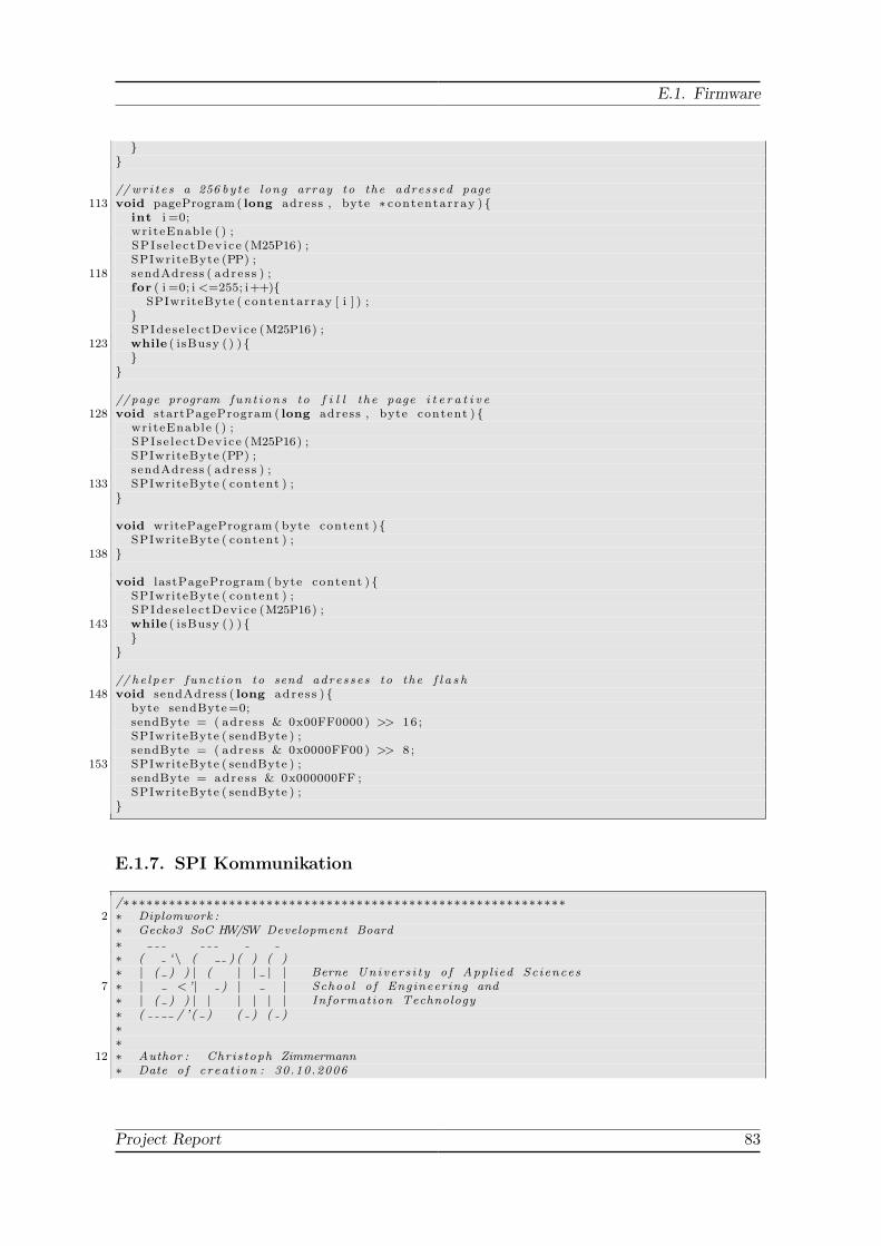
E.1. Firmware
}}
// wr i t e s a 256 by te long array to the adressed page113 void pageProgram ( long adress , byte ∗ contentar ray ) {
int i =0;wr iteEnable ( ) ;SPI s e l e c tDev i c e (M25P16) ;SPIwriteByte (PP) ;
118 sendAdress ( adre s s ) ;for ( i =0; i <=255; i++){
SPIwriteByte ( contentar ray [ i ] ) ;}SPIdese l e c tDev i ce (M25P16) ;
123 while ( isBusy ( ) ) {}
}
//page program fun t i on s to f i l l the page i t e r a t i v e128 void startPageProgram ( long adress , byte content ) {
writeEnable ( ) ;SPI s e l e c tDev i c e (M25P16) ;SPIwriteByte (PP) ;sendAdress ( adre s s ) ;
133 SPIwriteByte ( content ) ;}
void writePageProgram ( byte content ) {SPIwriteByte ( content ) ;
138 }
void lastPageProgram ( byte content ) {SPIwriteByte ( content ) ;SPIdese l e c tDev i ce (M25P16) ;
143 while ( isBusy ( ) ) {}
}
// he l pe r func t i on to send adres se s to the f l a s h148 void sendAdress ( long adre s s ) {
byte sendByte=0;sendByte = ( adre s s & 0x00FF0000 ) >> 16 ;SPIwriteByte ( sendByte ) ;sendByte = ( adre s s & 0x0000FF00 ) >> 8 ;
153 SPIwriteByte ( sendByte ) ;sendByte = adre s s & 0x000000FF ;SPIwriteByte ( sendByte ) ;
}
E.1.7. SPI Kommunikation
/∗ ∗∗∗∗∗∗∗∗∗∗∗∗∗∗∗∗∗∗∗∗∗∗∗∗∗∗∗∗∗∗∗∗∗∗∗∗∗∗∗∗∗∗∗∗∗∗∗∗∗∗∗∗∗∗∗∗∗∗2 ∗ Diplomwork :
∗ Gecko3 SoC HW/SW Development Board∗∗ ( ‘\ ( ) ( ) ( )∗ | ( ) ) | ( | | | | Berne Unive r s i t y o f Appl ied Sciences
7 ∗ | < ’| ) | | School o f Engineering and∗ | ( ) ) | | | | | | Information Technology∗ ( / ’( ) ( ) ( )∗∗
12 ∗ Author : Chris toph Zimmermann∗ Date o f c rea t i on : 30.10.2006
Project Report 83

E. Quellcode
∗ Descr ip t ion :∗ Library to access SPI Devices∗
17 ∗∗∗∗∗∗∗∗∗∗∗∗∗∗∗∗∗∗∗∗∗∗∗∗∗∗∗∗∗∗∗∗∗∗∗∗∗∗∗∗∗∗∗∗∗∗∗∗∗∗∗∗∗∗∗∗∗∗ ∗/
#include ” sp i . h”
void SPIse l e c tDev i c e ( byte dev i ce ) {22 switch ( dev i c e ) {
case 0 : DEVICE0 = 0 ;break ;
// case 1 : DEVICE1 = 0;// break ;
27 // case 2 : DEVICE2 = 0;// break ;
default : break ;}
}32
void SPIdese l e c tDev i ce ( byte dev i ce ) {switch ( dev i c e ) {
case 0 : DEVICE0 = 1 ;break ;
37 // case 1 : DEVICE1 = 1;// break ;// case 2 : DEVICE2 = 1;// break ;
default : break ;42 }
}
void SPIwriteByte ( byte outputdata ) {byte i =8;
47for ( i ; i >0; i−−){
SCLK = 0 ;i f ( outputdata > 127) {
MOSI = 1 ;52 }
else {MOSI = 0 ;
}SCLK = 1 ;
57 outputdata = outputdata << 1 ;}SCLK = 0 ;
}
62 byte SPIreadByte ( ) {byte i =0;byte inputdata =0;
SCLK = 0 ;67
for ( i ; i <7; i++){SCLK = 1 ;i f (MISO==1){
inputdata+=1;72 }
SCLK = 0 ;inputdata = inputdata << 1 ;
}SCLK = 1 ;
77 i f (MISO==1){inputdata+=1;
}
84 Matthias Zurbrugg, Christoph Zimmermann

E.1. Firmware
SCLK = 0 ;
82 return inputdata ;}
E.1.8. Kommunikation zwischen Host und FPGA
/∗ ∗∗∗∗∗∗∗∗∗∗∗∗∗∗∗∗∗∗∗∗∗∗∗∗∗∗∗∗∗∗∗∗∗∗∗∗∗∗∗∗∗∗∗∗∗∗∗∗∗∗∗∗∗∗∗∗∗∗∗ Diplomwork :∗ Gecko3 SoC HW/SW Development Board∗
5 ∗ ( ‘\ ( ) ( ) ( )∗ | ( ) ) | ( | | | | Berne Unive r s i t y o f Appl ied Sciences∗ | < ’| ) | | School o f Engineering and∗ | ( ) ) | | | | | | Information Technology∗ ( / ’( ) ( ) ( )
10 ∗∗∗ Author : Matthias Zurbrugg∗ Date o f c rea t i on : 16.11.2006∗ Descr ip t ion :
15 ∗ Source code o f read/wr i t e waveforms func t i ons∗∗∗∗∗∗∗∗∗∗∗∗∗∗∗∗∗∗∗∗∗∗∗∗∗∗∗∗∗∗∗∗∗∗∗∗∗∗∗∗∗∗∗∗∗∗∗∗∗∗∗∗∗∗∗∗∗∗∗ ∗/
#include ” fx2 . h”20 #include ” f x2 r e g s . h”
#include ” fx2 sd l y . h”
#define GPIFREAD 4 // read b i t in GPIFTRIG r e g i s t e r#define GPIF EP6 2 // EP6 b i t in GPIFTRIG r e g i s t e r
25 #define GPIF EP8 3 // EP8 b i t in GPIFTRIG r e g i s t e r
BYTE temp = 0 , i ; // temporary v a r i a b l e s f o r GPIF s t a t e machine breakcond i t i on
stat ic WORD FIFOBC IN = 0x0000 ; // v a r i a b l e t ha t conta ins EP6FIFOBCH/L va luestat ic WORD xdata Tcount = 0x01 ; // s e t t ransac t i on count to one fo r run the
read waveform one times30
void gpi f wr waveform (void ){
i f ( GPIFTRIG & 0x80 ) // i f GPIF i n t e r f a c e IDLE{
35 EP6GPIFFLGSEL = 0x01 ; // Set GPIF FIFO f l a g i f EP2 i s emptySYNCDELAY;
GPIFTRIG = GPIF EP6 ; // launch GPIF FIFO WRITE Transaction fromEP6 FIFO
SYNCDELAY;
40 do{
temp=(IOE&0x07 ) ; // read GPIF debug pins PE[ 0 : 2 ] f o r l ook ing thecurrent s t a t e ( show GSTAT in TRM)
i f ( temp==(IOE&0x07 ) ) // i f GPIF in the same s t a t e{
45 for ( i =0; i <3; i++){} // wait s e v e r a l timei f ( temp==(IOE&0x07 ) ) // i f GPIF in the same s t a t e{
for ( i =0; i <10; i++){} // wait s e v e r a l timei f ( temp==(IOE&0x07 ) ) // i f GPIF in the same s t a t e
50 {GPIFABORT = 0xFF ; // the GPIF s t a t e machine i s looked in a s t a t e and
must be abortedSYNCDELAY;
Project Report 85

E. Quellcode
FIFORESET = 0x80 ; // s e t NAKALL b i t to NAK a l l t r an s f e r s from hos tSYNCDELAY;
55 FIFORESET = 0x06 ; // r e s e t EP6 FIFOSYNCDELAY;FIFORESET = 0x00 ; // c l e a r NAKALL b i t to resume normal opera t ionSYNCDELAY;
}60 }
}} while ( ! ( GPIFTRIG & 0x80 ) ) ; // wait f o r DONE b i t from waveform
SYNCDELAY;65 EP6BCL = 0x00 ;
SYNCDELAY;EP6BCL = 0x80 ; // rearm EP2OUT
SYNCDELAY;}
70 }
void gp i f rd wave form (void ){
EP8GPIFFLGSEL = 0x10 ; // s e t GPIF FIFO f l a g to f u l l75 i f ( GPIFTRIG & 0x80 ) // i f GPIF i n t e r f a c e IDLE
{i f ( ! ( EP2468STAT & bmEP8FULL ) ) // check EP8 FULL( busy ) b i t in EP2468STAT
(SFR) , core s e t ’ s t h i s b i t when FIFO i s f u l l{
GPIFTCB1 = MSB( Tcount ) ; // se tup t ransac t i on count with Tcountva lue
80 SYNCDELAY;GPIFTCB0 = LSB( Tcount ) ;
SYNCDELAY;GPIFTRIG = GPIFREAD | GPIF EP8 ; // launch GPIF FIFO READ Transaction to
EP8IN ( p o l l i n g )85 SYNCDELAY;
do{
temp=(IOE&0x07 ) ; // read GPIF debug pins PE[ 0 : 2 ] f o r l ook ing thecurrent s t a t e ( show GSTAT in TRM)
i f ( temp==(IOE&0x07 ) ) // i f GPIF in the same s t a t e90 {
for ( i =0; i <4; i++){} // wait s e v e r a l timei f ( temp==(IOE&0x07 ) ) // i f GPIF in the same s t a t e{
for ( i =0; i <10; i++){} // wait s e v e r a l time95 i f ( temp==(IOE&0x07 ) ) // i f GPIF in the same s t a t e
{GPIFABORT = 0xFF ; // the GPIF s t a t e machine i s looked in a s t a t e
and must be abor ted}
}100 }
} while ( ! ( GPIFTRIG & 0x80 ) ) ; // wait f o r DONE b i t from waveform
SYNCDELAY;FIFOBC IN = ( ( EP8FIFOBCH << 8 ) + EP8FIFOBCL ) ; // ge t by te counter o f EP8IN
105i f ( FIFOBC IN < 0x0200 ) // i f packet i s shor t than a f u l l FIFO
bu f f e r{
INPKTEND = 0x08 ; // fo rce a commit to the hos t}
110 }}
}
86 Matthias Zurbrugg, Christoph Zimmermann

E.1. Firmware
E.1.9. GPIF Waveform Source Code
// This program con f i gu r e s the General Programmable In t e r f a c e (GPIF) fo r FX2.// Please do not modify s e c t i on s o f t e x t which are marked as ”DO NOT EDIT . . . ” .
3 //// DO NOT EDIT . . .// GPIF I n i t i a l i z a t i o n// In t e r f a c e Timing Sync// In t e rna l Ready I n i t IntRdy=1
8 // CTL Out Tr i s ta te−ab l e Binary// Sing leWri te WF Se l e c t 3// SingleRead WF Se l e c t 2// FifoWrite WF Se l e c t 1// FifoRead WF Se l e c t 0
13 // Data Bus I d l e Drive Tr i s t a t e// END DO NOT EDIT
// DO NOT EDIT . . .// GPIF Wave Names
18 // Wave 0 = FIFORd// Wave 1 = FIFOWr// Wave 2 = SnglWr2// Wave 3 = SnglWr1
23 // GPIF Ctr l Outputs Leve l// CTL 0 = WRU CMOS// CTL 1 = WRU CMOS// CTL 2 = RDYU CMOS// CTL 3 = unused CMOS
28 // CTL 4 = unused CMOS// CTL 5 = unused CMOS
// GPIF Rdy Inputs// RDY0 = WRX
33 // RDY1 = RDYX// RDY2 = unused// RDY3 = unused// RDY4 = unused// RDY5 = TCXpire
38 // FIFOFlag = FIFOFlag// IntReady = IntReady// END DO NOT EDIT// DO NOT EDIT . . .//
43 // GPIF Waveform 0: FIFORd//// In t e r v a l 0 1 2 3 4 5 6
I d l e (7)//
//48 // AddrMode Same Val Same Val Same Val Same Val Same Val Same Val Same Val
// DataMode NO Data NO Data NO Data Act i va te NO Data NO Data NO Data// NextData SameData SameData SameData SameData NextData SameData SameData// In t Trig No Int No Int No Int No Int No Int No Int No Int// IF/Wait IF IF IF Wait 1 IF IF IF
53 // Term A WRX FIFOFlag WRX WRX WRX RDYX// LFunc AND AND AND OR AND AND// Term B WRX FIFOFlag WRX RDYX WRX RDYX// Branch1 Then 1 Then 2 Then 2 Then 5 Then 1 Then 6// Branch0 Else 0 Else 1 Else 3 Else 4 Else 6 E l s e I d l e
58 // Re−Exec No No No No No No// Sngl /CRC Defau l t De fau l t De fau l t De fau l t De fau l t De fau l t De fau l t// WRU 0 0 0 0 0 0 0
0
Project Report 87

E. Quellcode
// WRU 0 0 0 0 0 0 00
// RDYU 0 0 1 1 0 0 10
63 // unused 0 0 0 0 0 0 00
// unused 0 0 0 0 0 0 00
// unused 0 0 0 0 0 0 00
//// END DO NOT EDIT
68 // DO NOT EDIT . . .//// GPIF Waveform 1: FIFOWr//// In t e r v a l 0 1 2 3 4 5 6
I d l e (7)73 //
//// AddrMode Same Val Same Val Same Val Same Val Same Val Same Val Same Val// DataMode NO Data NO Data Act i va te NO Data NO Data NO Data NO Data// NextData SameData SameData SameData NextData SameData SameData SameData
78 // In t Trig No Int No Int No Int No Int No Int No Int No Int// IF/Wait IF IF Wait 1 IF IF IF Wait 1// Term A WRX RDYX FIFOFlag RDYX RDYX// LFunc OR AND AND AND AND// Term B RDYX RDYX FIFOFlag RDYX RDYX
83 // Branch1 Then 0 Then 2 Then 4 Then 4 ThenIdle// Branch0 Else 1 Else 1 Else 0 Else 5 Else 5// Re−Exec No No No No No// Sngl /CRC Defau l t De fau l t De fau l t De fau l t De fau l t De fau l t De fau l t// WRU 0 0 0 0 0 0 0
088 // WRU 0 1 1 0 0 0 0
0// RDYU 0 0 0 0 0 1 1
0// unused 0 0 0 0 0 0 0
0// unused 0 0 0 0 0 0 0
0// unused 0 0 0 0 0 0 0
093 //
// END DO NOT EDIT// DO NOT EDIT . . .//// GPIF Waveform 2: SnglWr2
98 //// In t e r v a l 0 1 2 3 4 5 6
I d l e (7)//
//// AddrMode Same Val Same Val Same Val Same Val Same Val Same Val Same Val
103 // DataMode NO Data NO Data NO Data NO Data NO Data NO Data NO Data// NextData SameData SameData SameData SameData SameData SameData SameData// In t Trig No Int No Int No Int No Int No Int No Int No Int// IF/Wait Wait 1 Wait 1 Wait 1 Wait 1 Wait 1 Wait 1 Wait 1// Term A
108 // LFunc// Term B// Branch1// Branch0
88 Matthias Zurbrugg, Christoph Zimmermann

E.1. Firmware
// Re−Exec113 // Sngl /CRC Defau l t De fau l t De fau l t De fau l t De fau l t De fau l t De fau l t
// WRU 0 0 0 0 0 0 00
// WRU 0 0 0 0 0 0 00
// RDYU 0 0 0 0 0 0 00
// unused 0 0 0 0 0 0 00
118 // unused 0 0 0 0 0 0 00
// unused 0 0 0 0 0 0 00
//// END DO NOT EDIT// DO NOT EDIT . . .
123 //// GPIF Waveform 3: SnglWr1//// In t e r v a l 0 1 2 3 4 5 6
I d l e (7)//
128 //// AddrMode Same Val Same Val Same Val Same Val Same Val Same Val Same Val// DataMode NO Data NO Data NO Data NO Data NO Data NO Data NO Data// NextData SameData SameData SameData SameData SameData SameData SameData// In t Trig No Int No Int No Int No Int No Int No Int No Int
133 // IF/Wait Wait 1 Wait 1 Wait 1 Wait 1 Wait 1 Wait 1 Wait 1// Term A// LFunc// Term B// Branch1
138 // Branch0// Re−Exec// Sngl /CRC Defau l t De fau l t De fau l t De fau l t De fau l t De fau l t De fau l t// WRU 0 0 0 0 0 0 0
0// WRU 0 0 0 0 0 0 0
0143 // RDYU 0 0 0 0 0 0 0
0// unused 0 0 0 0 0 0 0
0// unused 0 0 0 0 0 0 0
0// unused 0 0 0 0 0 0 0
0//
148 // END DO NOT EDIT
// GPIF Program Code
// DO NOT EDIT . . .153 #include ” fx2 . h”
#include ” f x2 r e g s . h”#include ” fx2 sd l y . h” // SYNCDELAY macro// END DO NOT EDIT
158 // DO NOT EDIT . . .const char xdata WaveData [ 1 2 8 ] ={// Wave 0/∗ LenBr ∗/ 0x08 , 0x11 , 0x13 , 0x01 , 0x2C , 0x0E , 0x37 ,
0x07 ,
Project Report 89
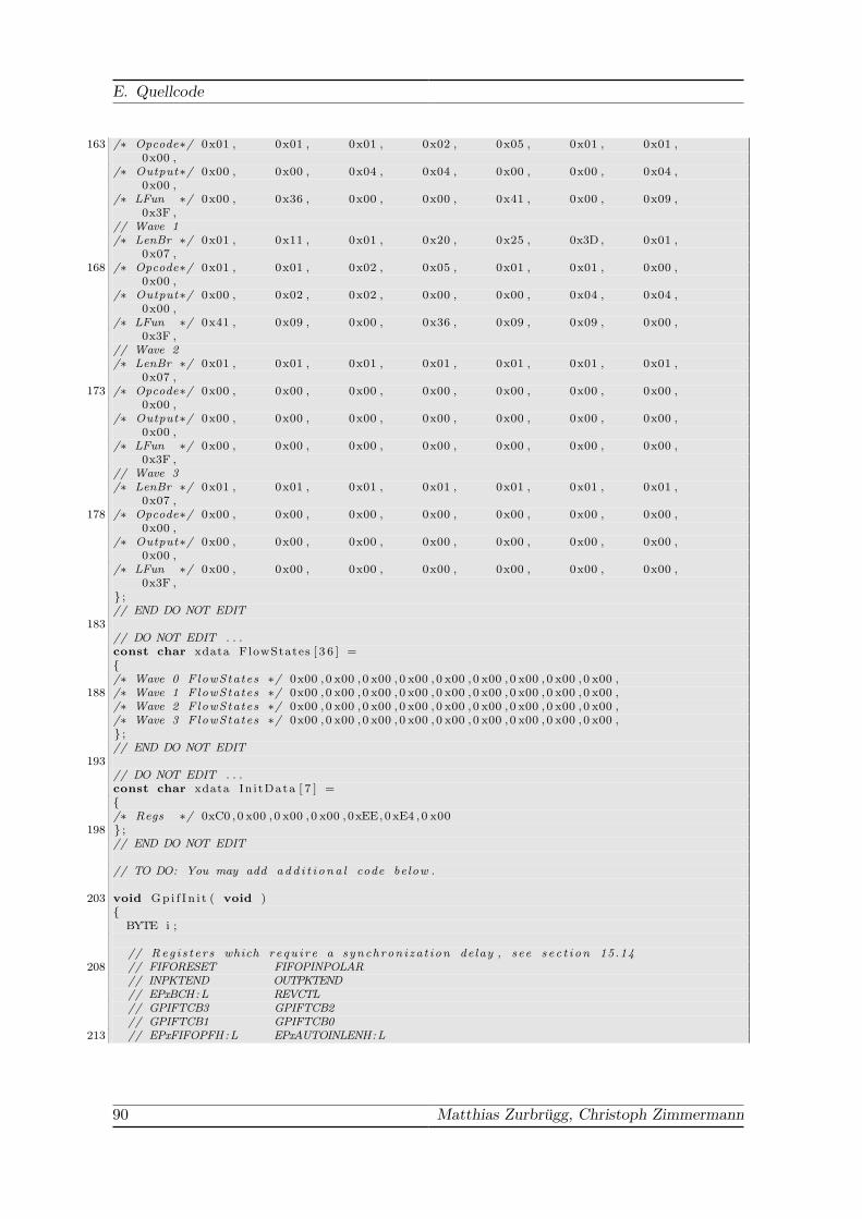
E. Quellcode
163 /∗ Opcode∗/ 0x01 , 0x01 , 0x01 , 0x02 , 0x05 , 0x01 , 0x01 ,0x00 ,
/∗ Output∗/ 0x00 , 0x00 , 0x04 , 0x04 , 0x00 , 0x00 , 0x04 ,0x00 ,
/∗ LFun ∗/ 0x00 , 0x36 , 0x00 , 0x00 , 0x41 , 0x00 , 0x09 ,0x3F ,
// Wave 1/∗ LenBr ∗/ 0x01 , 0x11 , 0x01 , 0x20 , 0x25 , 0x3D , 0x01 ,
0x07 ,168 /∗ Opcode∗/ 0x01 , 0x01 , 0x02 , 0x05 , 0x01 , 0x01 , 0x00 ,
0x00 ,/∗ Output∗/ 0x00 , 0x02 , 0x02 , 0x00 , 0x00 , 0x04 , 0x04 ,
0x00 ,/∗ LFun ∗/ 0x41 , 0x09 , 0x00 , 0x36 , 0x09 , 0x09 , 0x00 ,
0x3F ,// Wave 2/∗ LenBr ∗/ 0x01 , 0x01 , 0x01 , 0x01 , 0x01 , 0x01 , 0x01 ,
0x07 ,173 /∗ Opcode∗/ 0x00 , 0x00 , 0x00 , 0x00 , 0x00 , 0x00 , 0x00 ,
0x00 ,/∗ Output∗/ 0x00 , 0x00 , 0x00 , 0x00 , 0x00 , 0x00 , 0x00 ,
0x00 ,/∗ LFun ∗/ 0x00 , 0x00 , 0x00 , 0x00 , 0x00 , 0x00 , 0x00 ,
0x3F ,// Wave 3/∗ LenBr ∗/ 0x01 , 0x01 , 0x01 , 0x01 , 0x01 , 0x01 , 0x01 ,
0x07 ,178 /∗ Opcode∗/ 0x00 , 0x00 , 0x00 , 0x00 , 0x00 , 0x00 , 0x00 ,
0x00 ,/∗ Output∗/ 0x00 , 0x00 , 0x00 , 0x00 , 0x00 , 0x00 , 0x00 ,
0x00 ,/∗ LFun ∗/ 0x00 , 0x00 , 0x00 , 0x00 , 0x00 , 0x00 , 0x00 ,
0x3F ,} ;// END DO NOT EDIT
183// DO NOT EDIT . . .const char xdata FlowStates [ 3 6 ] ={/∗ Wave 0 FlowStates ∗/ 0x00 , 0 x00 , 0 x00 , 0 x00 , 0 x00 , 0 x00 , 0 x00 , 0 x00 , 0 x00 ,
188 /∗ Wave 1 FlowStates ∗/ 0x00 , 0 x00 , 0 x00 , 0 x00 , 0 x00 , 0 x00 , 0 x00 , 0 x00 , 0 x00 ,/∗ Wave 2 FlowStates ∗/ 0x00 , 0 x00 , 0 x00 , 0 x00 , 0 x00 , 0 x00 , 0 x00 , 0 x00 , 0 x00 ,/∗ Wave 3 FlowStates ∗/ 0x00 , 0 x00 , 0 x00 , 0 x00 , 0 x00 , 0 x00 , 0 x00 , 0 x00 , 0 x00 ,} ;// END DO NOT EDIT
193// DO NOT EDIT . . .const char xdata In i tData [ 7 ] ={/∗ Regs ∗/ 0xC0 , 0 x00 , 0 x00 , 0 x00 , 0xEE,0 xE4 , 0 x00
198 } ;// END DO NOT EDIT
// TO DO: You may add add i t i ona l code below .
203 void Gp i f I n i t ( void ){
BYTE i ;
// Reg i s t e r s which requ i r e a synchron i za t ion delay , see s e c t i on 15.14208 // FIFORESET FIFOPINPOLAR
// INPKTEND OUTPKTEND// EPxBCH:L REVCTL// GPIFTCB3 GPIFTCB2// GPIFTCB1 GPIFTCB0
213 // EPxFIFOPFH:L EPxAUTOINLENH:L
90 Matthias Zurbrugg, Christoph Zimmermann
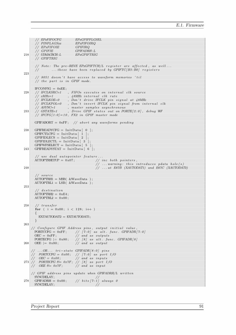
E.1. Firmware
// EPxFIFOCFG EPxGPIFFLGSEL// PINFLAGSxx EPxFIFOIRQ// EPxFIFOIE GPIFIRQ// GPIFIE GPIFADRH:L
218 // UDMACRCH:L EPxGPIFTRIG// GPIFTRIG
// Note : The pre−REVE EPxGPIFTCH/L r e g i s t e r are a f f e c t ed , as we l l . . .// . . . t h e s e have been rep laced by GPIFTC[B3 :B0 ] r e g i s t e r s
223// 8051 doesn ’ t have access to waveform memories ’ t i l// the par t i s in GPIF mode .
IFCONFIG = 0xEE;228 // IFCLKSRC=1 , FIFOs execu te s on i n t e r na l c l k source
// xMHz=1 , 48MHz in t e r na l c l k ra t e// IFCLKOE=0 , Don ’ t d r i v e IFCLK pin s i g n a l at 48MHz// IFCLKPOL=0 , Don ’ t i n v e r t IFCLK pin s i g n a l from in t e rna l c l k// ASYNC=1 , master samples asynchronous
233 // GSTATE=1 , Drive GPIF s t a t e s out on PORTE[ 2 : 0 ] , debug WF// IFCFG[1:0 ]=10 , FX2 in GPIF master mode
GPIFABORT = 0xFF ; // abor t any waveforms pending
238 GPIFREADYCFG = InitData [ 0 ] ;GPIFCTLCFG = InitData [ 1 ] ;GPIFIDLECS = InitData [ 2 ] ;GPIFIDLECTL = InitData [ 3 ] ;GPIFWFSELECT = InitData [ 5 ] ;
243 GPIFREADYSTAT = InitData [ 6 ] ;
// use dual au topo in te r f e a t u r e . . .AUTOPTRSETUP = 0x07 ; // inc both po in ters ,
// . . . warning : t h i s in t roduces pdata ho l e ( s )248 // . . . a t E67B (XAUTODAT1) and E67C (XAUTODAT2)
// sourceAUTOPTRH1 = MSB( &WaveData ) ;AUTOPTRL1 = LSB( &WaveData ) ;
253// de s t i na t i onAUTOPTRH2 = 0xE4 ;AUTOPTRL2 = 0x00 ;
258 // t r an s f e rfor ( i = 0x00 ; i < 128 ; i++ ){
EXTAUTODAT2 = EXTAUTODAT1;}
263// Configure GPIF Address pins , output i n i t i a l value ,
PORTCCFG = 0xFF ; // [ 7 : 0 ] as a l t . func . GPIFADR[ 7 : 0 ]OEC = 0xFF ; // and as outputsPORTECFG |= 0x80 ; // [ 8 ] as a l t . func . GPIFADR[ 8 ]
268 OEE |= 0x80 ; // and as output
// . . .OR. . . t r i−s t a t e GPIFADR[ 8 : 0 ] p ins// PORTCCFG = 0x00 ; // [ 7 : 0 ] as por t I /O// OEC = 0x00 ; // and as inpu t s
273 // PORTECFG &= 0x7F ; // [ 8 ] as por t I /O// OEE &= 0x7F ; // and as input
// GPIF address p ins update when GPIFADRH/L wr i t t enSYNCDELAY; //
278 GPIFADRH = 0x00 ; // b i t s [ 7 : 1 ] always 0SYNCDELAY; //
Project Report 91
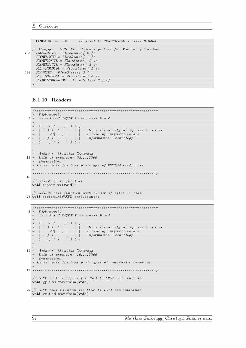
E. Quellcode
GPIFADRL = 0x00 ; // po in t to PERIPHERAL address 0x0000
/∗ Configure GPIF FlowStates r e g i s t e r s f o r Wave 0 o f WaveData283 FLOWSTATE = FlowStates [ 0 ] ;
FLOWLOGIC = FlowStates [ 1 ] ;FLOWEQ0CTL = FlowStates [ 2 ] ;FLOWEQ1CTL = FlowStates [ 3 ] ;FLOWHOLDOFF = FlowStates [ 4 ] ;
288 FLOWSTB = FlowStates [ 5 ] ;FLOWSTBEDGE = FlowStates [ 6 ] ;FLOWSTBHPERIOD = FlowStates [ 7 ] ; ∗/
}
E.1.10. Headers
/∗ ∗∗∗∗∗∗∗∗∗∗∗∗∗∗∗∗∗∗∗∗∗∗∗∗∗∗∗∗∗∗∗∗∗∗∗∗∗∗∗∗∗∗∗∗∗∗∗∗∗∗∗∗∗∗∗∗∗∗∗ Diplomwork :
3 ∗ Gecko3 SoC HW/SW Development Board∗∗ ( ‘\ ( ) ( ) ( )∗ | ( ) ) | ( | | | | Berne Unive r s i t y o f Appl ied Sciences∗ | < ’| ) | | School o f Engineering and
8 ∗ | ( ) ) | | | | | | Information Technology∗ ( / ’( ) ( ) ( )∗∗∗ Author : Matthias Zurbrugg
13 ∗ Date o f c rea t i on : 08.11.2006∗ Descr ip t ion :∗ Header with func t i on pro to type o f EEPROM read/wr i t e∗∗∗∗∗∗∗∗∗∗∗∗∗∗∗∗∗∗∗∗∗∗∗∗∗∗∗∗∗∗∗∗∗∗∗∗∗∗∗∗∗∗∗∗∗∗∗∗∗∗∗∗∗∗∗∗∗∗∗ ∗/
18// EEPROM wri t e func t i onvoid eeprom wr (void ) ;
// EEPROM read func t i on with number o f by t e s to read23 void eeprom rd (WORD read count ) ;
/∗ ∗∗∗∗∗∗∗∗∗∗∗∗∗∗∗∗∗∗∗∗∗∗∗∗∗∗∗∗∗∗∗∗∗∗∗∗∗∗∗∗∗∗∗∗∗∗∗∗∗∗∗∗∗∗∗∗∗∗2 ∗ Diplomwork :
∗ Gecko3 SoC HW/SW Development Board∗∗ ( ‘\ ( ) ( ) ( )∗ | ( ) ) | ( | | | | Berne Unive r s i t y o f Appl ied Sciences
7 ∗ | < ’| ) | | School o f Engineering and∗ | ( ) ) | | | | | | Information Technology∗ ( / ’( ) ( ) ( )∗∗
12 ∗ Author : Matthias Zurbrugg∗ Date o f c rea t i on : 16.11.2006∗ Descr ip t ion :∗ Header with func t i on pro to types o f read/wr i t e waveforms∗
17 ∗∗∗∗∗∗∗∗∗∗∗∗∗∗∗∗∗∗∗∗∗∗∗∗∗∗∗∗∗∗∗∗∗∗∗∗∗∗∗∗∗∗∗∗∗∗∗∗∗∗∗∗∗∗∗∗∗∗ ∗/
// GPIF wr i t e waveform for Host to FPGA communicationvoid gpi f wr waveform (void ) ;
22 // GPIF read waveform for FPGA to Host communicationvoid gp i f rd wave form (void ) ;
92 Matthias Zurbrugg, Christoph Zimmermann
E.1. Firmware
/∗ ∗∗∗∗∗∗∗∗∗∗∗∗∗∗∗∗∗∗∗∗∗∗∗∗∗∗∗∗∗∗∗∗∗∗∗∗∗∗∗∗∗∗∗∗∗∗∗∗∗∗∗∗∗∗∗∗∗∗2 ∗ Diplomwork :
∗ Gecko3 SoC HW/SW Development Board∗∗ ( ‘\ ( ) ( ) ( )∗ | ( ) ) | ( | | | | Berne Unive r s i t y o f Appl ied Sciences
7 ∗ | < ’| ) | | School o f Engineering and∗ | ( ) ) | | | | | | Information Technology∗ ( / ’( ) ( ) ( )∗∗
12 ∗ Author : Chris toph Zimmermann∗ Date o f c rea t i on : 30.10.2006∗ Descr ip t ion :∗ Header f i l e to use the SPI l i b r a r y∗
17 ∗ Changelog :∗ 30.10.2006∗ f i r s t ver s ion∗∗∗∗∗∗∗∗∗∗∗∗∗∗∗∗∗∗∗∗∗∗∗∗∗∗∗∗∗∗∗∗∗∗∗∗∗∗∗∗∗∗∗∗∗∗∗∗∗∗∗∗∗∗∗∗∗∗ ∗/
22 #include ” fx2 . h”#include ” f x2 r e g s . h”
#define MOSI PA1#define MISO PA2
27 #define SCLK PA0#define DEVICE0 PA3//#de f ine DEVICE1//#de f ine DEVICE2//#de f ine DEVICE3
32typedef unsigned char byte ;
void SPIse l e c tDev i c e ( byte dev i ce ) ;
37 void SPIdese l e c tDev i ce ( byte dev i ce ) ;
void SPIwriteByte ( byte outputdata ) ;
byte SPIreadByte (void ) ;
/∗ ∗∗∗∗∗∗∗∗∗∗∗∗∗∗∗∗∗∗∗∗∗∗∗∗∗∗∗∗∗∗∗∗∗∗∗∗∗∗∗∗∗∗∗∗∗∗∗∗∗∗∗∗∗∗∗∗∗∗∗ Diplomwork :∗ Gecko3 SoC HW/SW Development Board
4 ∗∗ ( ‘\ ( ) ( ) ( )∗ | ( ) ) | ( | | | | Berne Unive r s i t y o f Appl ied Sciences∗ | < ’| ) | | School o f Engineering and∗ | ( ) ) | | | | | | Information Technology
9 ∗ ( / ’( ) ( ) ( )∗∗∗ Author : Matthias Zurbrugg∗ Date o f c rea t i on : 31.10.2006
14 ∗ Descr ip t ion :∗ Header with func t i on pro to type o f FPGA con f i gu ra t i on from Host over USB∗∗∗∗∗∗∗∗∗∗∗∗∗∗∗∗∗∗∗∗∗∗∗∗∗∗∗∗∗∗∗∗∗∗∗∗∗∗∗∗∗∗∗∗∗∗∗∗∗∗∗∗∗∗∗∗∗∗∗ ∗/
19 // i n i t i a l i s a t i o n fo r FPGA con f i gu ra t i onvoid f p g a c f g i n i t (void ) ;
// func t ion tha t con f i gure the FPGAvoid f p g a c f g (void ) ;
Project Report 93
E. Quellcode
/∗ ∗∗∗∗∗∗∗∗∗∗∗∗∗∗∗∗∗∗∗∗∗∗∗∗∗∗∗∗∗∗∗∗∗∗∗∗∗∗∗∗∗∗∗∗∗∗∗∗∗∗∗∗∗∗∗∗∗∗2 ∗ Diplomwork :
∗ Gecko3 SoC HW/SW Development Board∗∗ ( ‘\ ( ) ( ) ( )∗ | ( ) ) | ( | | | | Berne Unive r s i t y o f Appl ied Sciences
7 ∗ | < ’| ) | | School o f Engineering and∗ | ( ) ) | | | | | | Information Technology∗ ( / ’( ) ( ) ( )∗∗
12 ∗ Author : Chris toph Zimmermann∗ Date o f c rea t i on : 31.10.2006∗ Descr ip t ion :∗ Header f i l e f o r the M25P16 Library∗ Library to access the M25P16 SPI Flash from ST
17 ∗ Microe l e c t ron i c s . The S25FL016 SPI Flash from∗ Spansion i s so f tware and pin compat ib le∗∗ Changelog :∗ 31.10.2006
22 ∗ f i r s t ver s ion∗∗∗∗∗∗∗∗∗∗∗∗∗∗∗∗∗∗∗∗∗∗∗∗∗∗∗∗∗∗∗∗∗∗∗∗∗∗∗∗∗∗∗∗∗∗∗∗∗∗∗∗∗∗∗∗∗∗ ∗/
// de f i n e s wich dev i ce in the SPI subsytem i s the M25P16#define M25P16 0
27 #define MANUFACTURER 0x20#define MEMTYPE 0x20#define MEMCAPACITY 0x15
#define MAXADRESS 0x1FFFFF32
// f l a s h memory opcodes#define WREN 0x06#define WRDI 0x04#define RDID 0x9F
37 #define RDSR 0x05#define WRSR 0x01#define READ 0x03#define FAST READ 0x0B#define PP 0x02
42 #define SE 0xD8#define BE 0xC7#define DP 0xB9#define RES 0xAB
47 // checks i f the co r r ec t dev i ce i s s e l e c t e db i t isM25P16 ( ) ;
// checks i f the dev i ce i s busy or ready to r e c e i v e the next i n s t r u c t i onb i t isBusy ( ) ;
52// he l pe r func t i on to send adres se s to the f l a s hvoid sendAdress ( long adre s s ) ;
// enab le wr i t e access57 void writeEnable ( ) ;
// read one by te at the g iven adressbyte readByte ( long adre s s ) ;
62 // s t a r t s a b l o c k read from the g iven adressbyte startBlockRead ( long adre s s ) ;
// reads the next by te ( s e q u en t i a l readout )byte readBlock ( ) ;
94 Matthias Zurbrugg, Christoph Zimmermann
E.2. Loopback Core
67// reads the l a s t by te from a b l ock and terminates the b lockreadbyte lastBlockRead ( ) ;
// erases the s e c t o r in wich the g iven adress i s72 void s e c to rEra s e ( long adre s s ) ;
// erases the whole f l a s hvoid bulkErase ( ) ;
77 // wr i t e s a 256 by te long array to the adressed pagevoid pageProgram ( long adress , byte ∗ contentar ray ) ;
//page program fun t i on s to f i l l the page i t e r a t i v evoid startPageProgram ( long adress , byte content ) ;
82void writePageProgram ( byte content ) ;
void lastPageProgram ( byte content ) ;
/∗ ∗∗∗∗∗∗∗∗∗∗∗∗∗∗∗∗∗∗∗∗∗∗∗∗∗∗∗∗∗∗∗∗∗∗∗∗∗∗∗∗∗∗∗∗∗∗∗∗∗∗∗∗∗∗∗∗∗∗∗ Diplomwork :∗ Gecko3 SoC HW/SW Development Board∗
5 ∗ ( ‘\ ( ) ( ) ( )∗ | ( ) ) | ( | | | | Berne Unive r s i t y o f Appl ied Sciences∗ | < ’| ) | | School o f Engineering and∗ | ( ) ) | | | | | | Information Technology∗ ( / ’( ) ( ) ( )
10 ∗∗∗ Author : Matthias Zurbrugg∗ Date o f c rea t i on : 30.10.2006∗ Descr ip t ion :
15 ∗ Header with func t i on pro to types o f SPI Flash read/wr i t e and the∗ au tocon f i gu ra t i on∗∗∗∗∗∗∗∗∗∗∗∗∗∗∗∗∗∗∗∗∗∗∗∗∗∗∗∗∗∗∗∗∗∗∗∗∗∗∗∗∗∗∗∗∗∗∗∗∗∗∗∗∗∗∗∗∗∗∗ ∗/
20 // i n i t i a l i s a t i o n fo r SPI Flash communicationvoid s p i f l a s h i n i t (void ) ;
// SPI Flash wr i t e func t i onvoid s p i f l a s h w r (void ) ;
25// SPI Flash read func t ionvoid s p i f l a s h r d (void ) ;
// Booload func t i on tha t con f i gure the FPGA from SPI Flash30 void boo t l oad c f g (void ) ;
E.2. Loopback Core
E.2.1. Top
−−−−−−−−−−−−−−−−−−−−−−−−−−−−−−−−−−−−−−−−−−−−−−−−−−−−−−−−−−−−−−−−−−−−−−−−−−−−−−−−−−−− Diplomwork :−− Gecko3 SoC HW/SW Development Board−−
5 −− ( ‘\ ( ) ( ) ( )−− | ( ) ) | ( | | | | Berne Unive r s i t y o f Appl ied Sciences−− | < ’| ) | | School o f Engineering and
Project Report 95

E. Quellcode
−− | ( ) ) | | | | | | Information Technology−− ( / ’( ) ( ) ( )
10 −−−−−− Author : Chris toph Zimmermann−− Date o f c rea t i on : 8 .11.2006−− Descr ip t ion :
15 −− FPGA Module to t e s t the communication between the EZ−USB and the FPGA.−− The EZ−USB sends data (16 b i t wide ) to the FPGA. they are s to red and when−− the s e l e c t e d number o f data ( s e l e c t e d by the sw i t che s ) i s reached the FPGA−− s t a r t s to send back the data to the EZ−USB in reversed order (FILO)−−
20 −− Target Devices : X i l inx Spartan3 FPGA’ s ( usage o f BlockRam in the Datapath )−− Tool ve r s i ons : 8.2 i−− Dependencies :−−−−
25 −−−−−−−−−−−−−−−−−−−−−−−−−−−−−−−−−−−−−−−−−−−−−−−−−−−−−−−−−−−−−−−−−−−−−−−−−−−−−−−−−−
l ibrary IEEE ;use IEEE . STD LOGIC 1164 .ALL;use IEEE .STD LOGIC ARITH.ALL;
30 use IEEE .STD LOGIC UNSIGNED.ALL;
−−−− Uncomment the f o l l ow i n g l i b r a r y de c l a ra t i on i f i n s t a n t i a t i n g−−−− any Xi l inx p r im i t i v e s in t h i s code .l ibrary UNISIM ;
35 use UNISIM . VComponents . a l l ;
entity loopback i sport (
DATA: inout s t d l o g i c v e c t o r (15 downto 0) ;40 CLK, RESET, WRU, RDYU: in s t d l o g i c ; −−r e s e t but ton on development board i s 1
when pressedWRX, RDYX, PW: out s t d l o g i c
) ;end loopback ;
45 architecture Behaviora l of loopback i s
signal up , down , zero , writeEN , we : s t d l o g i c ;signal WRUint , RDYUint : s t d l o g i c ;
50 component STMPORT (
CLK, RDYU, RESET, WRU, zero : IN s t d l o g i c ;down , RDYX, up , we , writeEN , WRX : OUT s t d l o g i c
) ;55 end component ;
component datapathport (
c lk , r e s e t , we , up , down , writeEN : IN s t d l o g i c ;60 zero : OUT s t d l o g i c ;
data : inout s t d l o g i c v e c t o r (15 downto 0)) ;
end component ;
65 begin
PW <= ’1 ’ ; −−power led , to show tha t the core i s loaded
−−doub le b u f f e r i n g o f the stm inpu t s70 process ( c lk , r e s e t )
begini f r e s e t = ’1 ’ then
96 Matthias Zurbrugg, Christoph Zimmermann

E.2. Loopback Core
WRUint <= ’0 ’ ;RDYUint <= ’0 ’ ;
75 e l s i f c l k = ’1 ’ and c lk ’ event then
WRUint <= WRU;
RDYUint <= RDYU;80 end i f ;
end process ;
i s tm : STMport map(
85 CLK => CLK, RESET => RESET, WRU => WRUint , WRX => WRX, RDYU => RDYUint , RDYX =>RDYX,
zero => zero , writeEN => writeEN , we => we , up => up , down => down) ;
i datapath : datapathport map(
90 c l k => CLK, r e s e t => RESET, zero => zero , we => we , up => up , down => down ,writeEN => writeEN , data => DATA
) ;
end Behaviora l ;
E.2.2. Datenpfad
1 −−−−−−−−−−−−−−−−−−−−−−−−−−−−−−−−−−−−−−−−−−−−−−−−−−−−−−−−−−−−−−−−−−−−−−−−−−−−−−−−−−−− Diplomwork :−− Gecko3 SoC HW/SW Development Board−−−− ( ‘\ ( ) ( ) ( )
6 −− | ( ) ) | ( | | | | Berne Unive r s i t y o f Appl ied Sciences−− | < ’| ) | | School o f Engineering and−− | ( ) ) | | | | | | Information Technology−− ( / ’( ) ( ) ( )−−
11 −−−− Author : Chris toph Zimmermann−− Date o f c rea t i on : 8 .11.2006−− Descr ip t ion :−− Datapath f o r the loopback module
16 −−−− Target Devices : X i l inx Spartan3 FPGA’ s ( usage o f BlockRam in the Datapath )−− Tool ve r s i ons : 8.2 i−− Dependencies :−−
21 −−−−−−−−−−−−−−−−−−−−−−−−−−−−−−−−−−−−−−−−−−−−−−−−−−−−−−−−−−−−−−−−−−−−−−−−−−−−−−−−−−−−
l ibrary IEEE ;use IEEE . STD LOGIC 1164 .ALL;
26 use IEEE .STD LOGIC ARITH.ALL;use IEEE .STD LOGIC UNSIGNED.ALL;
−−−− Uncomment the f o l l ow i n g l i b r a r y de c l a ra t i on i f i n s t a n t i a t i n g−−−− any Xi l inx p r im i t i v e s in t h i s code .
31 l ibrary UNISIM ;use UNISIM . VComponents . a l l ;
entity datapath i sport (
36 c lk , r e s e t , we , up , down , writeEN : IN s t d l o g i c ;ze ro : OUT s t d l o g i c ;data : inout s t d l o g i c v e c t o r (15 downto 0)
Project Report 97
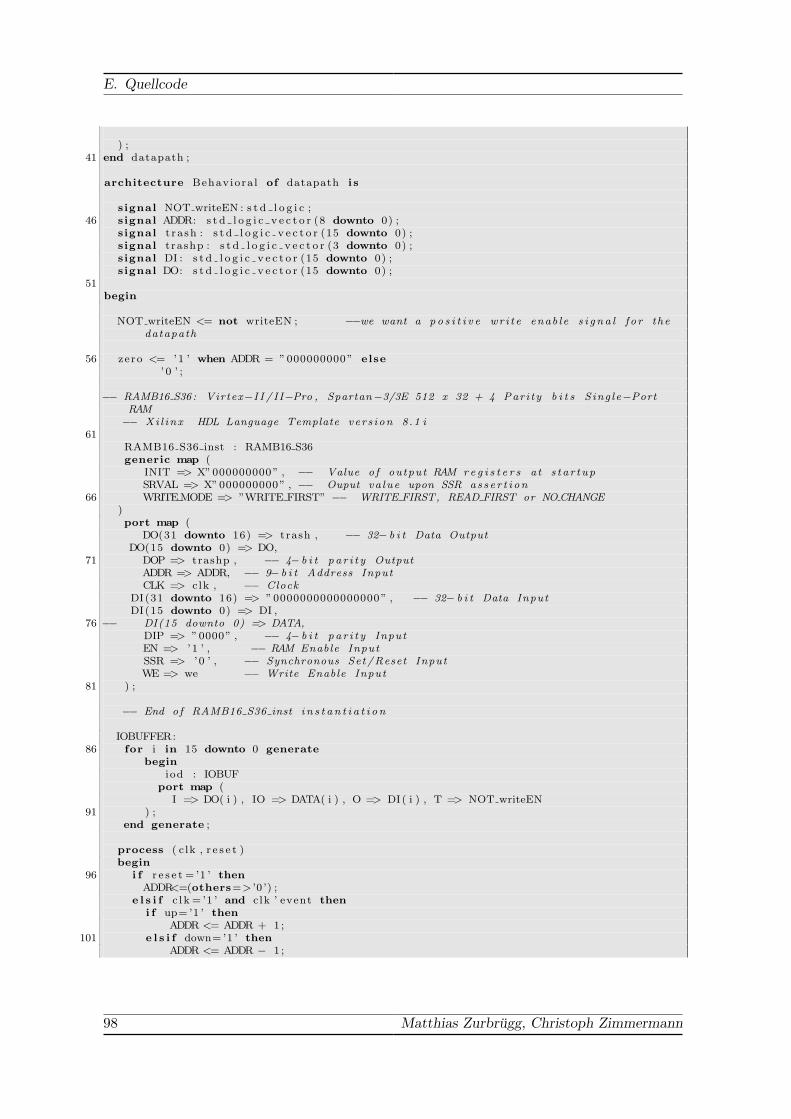
E. Quellcode
) ;41 end datapath ;
architecture Behaviora l of datapath i s
signal NOT writeEN : s t d l o g i c ;46 signal ADDR: s t d l o g i c v e c t o r (8 downto 0) ;
signal t ra sh : s t d l o g i c v e c t o r (15 downto 0) ;signal trashp : s t d l o g i c v e c t o r (3 downto 0) ;signal DI : s t d l o g i c v e c t o r (15 downto 0) ;signal DO: s t d l o g i c v e c t o r (15 downto 0) ;
51begin
NOT writeEN <= not writeEN ; −−we want a p o s i t i v e wr i t e enab le s i g n a l f o r thedatapath
56 zero <= ’1 ’ when ADDR = ”000000000” else’ 0 ’ ;
−− RAMB16 S36 : Virtex−I I / II−Pro , Spartan−3/3E 512 x 32 + 4 Pari ty b i t s S ing le−PortRAM
−− Xi l inx HDL Language Template ver s ion 8.1 i61
RAMB16 S36 inst : RAMB16 S36generic map (
INIT => X”000000000” , −− Value o f output RAM r e g i s t e r s at s t a r t upSRVAL => X”000000000” , −− Ouput va lue upon SSR as s e r t i on
66 WRITE MODE => ”WRITE FIRST” −− WRITE FIRST, READ FIRST or NO CHANGE)port map (
DO(31 downto 16) => trash , −− 32− b i t Data OutputDO(15 downto 0) => DO,
71 DOP => trashp , −− 4− b i t p a r i t y OutputADDR => ADDR, −− 9− b i t Address InputCLK => c lk , −− Clock
DI(31 downto 16) => ”0000000000000000” , −− 32− b i t Data InputDI(15 downto 0) => DI ,
76 −− DI(15 downto 0) => DATA,DIP => ”0000” , −− 4− b i t p a r i t y InputEN => ’ 1 ’ , −− RAM Enable InputSSR => ’ 0 ’ , −− Synchronous Set /Reset InputWE => we −− Write Enable Input
81 ) ;
−− End of RAMB16 S36 inst i n s t a n t i a t i o n
IOBUFFER:86 for i in 15 downto 0 generate
begini od : IOBUF
port map (I => DO( i ) , IO => DATA( i ) , O => DI( i ) , T => NOT writeEN
91 ) ;end generate ;
process ( c lk , r e s e t )begin
96 i f r e s e t = ’1 ’ thenADDR<=(others=> ’0 ’) ;
e l s i f c l k = ’1 ’ and c lk ’ event theni f up= ’1 ’ then
ADDR <= ADDR + 1 ;101 e l s i f down= ’1 ’ then
ADDR <= ADDR − 1 ;
98 Matthias Zurbrugg, Christoph Zimmermann
E.2. Loopback Core
end i f ;end i f ;
end process ;106
end Behaviora l ;
E.2.3. Statemachine
−− C:\DOCUMENTS AND SETTINGS\ZIMMC5\GECKO3 LOOPBACK\STM. vhd2 −− VHDL code crea ted by Xi l inx ’ s StateCAD 8.2 i−− Fri Dec 08 10:49:11 2006
−− This VHDL code ( f o r use with Xi l inx XST) was generated us ing :−− enumerated s t a t e assignment with s t ruc tu r ed code format .
7 −− Minimization i s enabled , imp l i ed e l s e i s enabled ,−− and outputs are speed opt imized .
LIBRARY i e e e ;USE i e e e . s t d l o g i c 1 1 6 4 . a l l ;
12ENTITY STM IS
PORT (CLK,RDYU,RESET,WRU, zero : IN s t d l o g i c ;down ,RDYX, up , we , writeEN ,WRX : OUT s t d l o g i c ) ;
END;17
ARCHITECTURE BEHAVIOR OF STM ISTYPE t ype s r e g IS (ADRESS UP,CHECK END,CHECKWRU,END PACKET,GET REQUEST, IDLE
,PKTEND,SAVE DATA,SEND DATA,SEND REQUEST,VALID DATA,WAIT END) ;SIGNAL sreg , n ex t s r e g : t ype s r e g ;
22 SIGNAL next down , next RDYX , next up , next we , next writeEN , next WRX :s t d l o g i c ;
BEGINPROCESS (CLK, RESET, next s reg , next down , next RDYX , next up , next we ,
next writeEN , next WRX)27 BEGIN
IF ( RESET= ’1 ’ ) THENs r eg <= IDLE ;down <= ’0 ’ ;RDYX <= ’0 ’ ;
32 up <= ’0 ’ ;we <= ’0 ’ ;writeEN <= ’0 ’ ;WRX <= ’0 ’ ;
ELSIF CLK= ’1 ’ AND CLK’ event THEN37 s r eg <= next s r e g ;
down <= next down ;RDYX <= next RDYX ;up <= next up ;we <= next we ;
42 writeEN <= next writeEN ;WRX <= next WRX ;
END IF ;END PROCESS;
47 PROCESS ( sreg ,RDYU,WRU, zero )BEGIN
next down <= ’0 ’ ; next RDYX <= ’0 ’ ; next up <= ’0 ’ ; next we <= ’0 ’ ;next writeEN <= ’0 ’ ; next WRX <= ’0 ’ ;
52 next s reg<=ADRESS UP;
CASE s r eg ISWHEN ADRESS UP =>
next s reg<=IDLE ;
Project Report 99

E. Quellcode
57 next writeEN <=’0 ’;next we <=’0 ’;next up <=’0 ’;next down <=’0 ’;next WRX<=’0 ’;
62 next RDYX<=’0 ’;WHEN CHECK END =>
IF ( ze ro = ’1 ’ ) THENnext s reg<=END PACKET;next writeEN <=’0 ’;
67 next we <=’0 ’;next up <=’0 ’;next down <=’0 ’;next WRX<=’0 ’;next RDYX<=’1 ’;
72 END IF ;IF ( ze ro = ’0 ’ ) THEN
next s reg<=CHECKWRU;next writeEN <=’0 ’;next we <=’0 ’;
77 next up <=’0 ’;next down <=’1 ’;next WRX<=’0 ’;next RDYX<=’0 ’;
END IF ;82 WHEN CHECKWRU =>
IF ( WRU= ’0 ’ ) THENnext s reg<=SEND REQUEST;next writeEN <=’0 ’;next we <=’0 ’;
87 next up <=’0 ’;next down <=’0 ’;next WRX<=’1 ’;next RDYX<=’0 ’;
ELSE92 next s reg<=CHECKWRU;
next writeEN <=’0 ’;next we <=’0 ’;next up <=’0 ’;next down <=’1 ’;
97 next WRX<=’0 ’;next RDYX<=’0 ’;
END IF ;WHEN END PACKET =>
IF ( RDYU= ’1 ’ ) THEN102 next s reg<=WAIT END;
next writeEN <=’0 ’;next we <=’0 ’;next up <=’0 ’;next down <=’0 ’;
107 next WRX<=’0 ’;next RDYX<=’0 ’;
ELSEnext s reg<=END PACKET;next writeEN <=’0 ’;
112 next we <=’0 ’;next up <=’0 ’;next down <=’0 ’;next WRX<=’0 ’;next RDYX<=’1 ’;
117 END IF ;WHEN GET REQUEST =>
IF ( WRU= ’0 ’ ) THENnext s reg<=SAVE DATA;next writeEN <=’0 ’;
122 next we <=’1 ’;
100 Matthias Zurbrugg, Christoph Zimmermann
E.2. Loopback Core
next up <=’0 ’;next down <=’0 ’;next WRX<=’0 ’;next RDYX<=’0 ’;
127 ELSEnext s reg<=GET REQUEST;next writeEN <=’0 ’;next we <=’0 ’;next up <=’0 ’;
132 next down <=’0 ’;next WRX<=’0 ’;next RDYX<=’1 ’;
END IF ;WHEN IDLE =>
137 IF ( RDYU= ’1 ’ AND WRU= ’1 ’ ) OR ( WRU= ’0 ’ AND RDYU= ’0 ’ ) THENnext s reg<=IDLE ;next writeEN <=’0 ’;next we <=’0 ’;next up <=’0 ’;
142 next down <=’0 ’;next WRX<=’0 ’;next RDYX<=’0 ’;
END IF ;IF ( WRU= ’1 ’ AND RDYU= ’0 ’ ) THEN
147 next s reg<=GET REQUEST;next writeEN <=’0 ’;next we <=’0 ’;next up <=’0 ’;next down <=’0 ’;
152 next WRX<=’0 ’;next RDYX<=’1 ’;
END IF ;IF ( WRU= ’0 ’ AND RDYU= ’1 ’ ) THEN
next s reg<=PKTEND;157 next writeEN <=’0 ’;
next we <=’0 ’;next up <=’0 ’;next down <=’0 ’;next WRX<=’0 ’;
162 next RDYX<=’1 ’;END IF ;
WHEN PKTEND =>IF ( RDYU= ’0 ’ ) THEN
next s reg<=CHECKWRU;167 next writeEN <=’0 ’;
next we <=’0 ’;next up <=’0 ’;next down <=’1 ’;next WRX<=’0 ’;
172 next RDYX<=’0 ’;ELSE
next s reg<=PKTEND;next writeEN <=’0 ’;next we <=’0 ’;
177 next up <=’0 ’;next down <=’0 ’;next WRX<=’0 ’;next RDYX<=’1 ’;
END IF ;182 WHEN SAVE DATA =>
next s reg<=ADRESS UP;next writeEN <=’0 ’;next we <=’0 ’;next up <=’1 ’;
187 next down <=’0 ’;next WRX<=’0 ’;
Project Report 101

E. Quellcode
next RDYX<=’0 ’;WHEN SEND DATA =>
next s reg<=VALID DATA;192 next writeEN <=’1 ’;
next we <=’0 ’;next up <=’0 ’;next down <=’0 ’;next WRX<=’0 ’;
197 next RDYX<=’0 ’;WHEN SEND REQUEST =>
IF ( RDYU= ’1 ’ ) THENnext s reg<=SEND DATA;next writeEN <=’1 ’;
202 next we <=’0 ’;next up <=’0 ’;next down <=’0 ’;next WRX<=’1 ’;next RDYX<=’0 ’;
207 ELSEnext s reg<=SEND REQUEST;next writeEN <=’0 ’;next we <=’0 ’;next up <=’0 ’;
212 next down <=’0 ’;next WRX<=’1 ’;next RDYX<=’0 ’;
END IF ;WHEN VALID DATA =>
217 IF ( RDYU= ’0 ’ ) THENnext s reg<=CHECK END;next writeEN <=’0 ’;next we <=’0 ’;next up <=’0 ’;
222 next down <=’0 ’;next WRX<=’0 ’;next RDYX<=’0 ’;
ELSEnext s reg<=VALID DATA;
227 next writeEN <=’1 ’;next we <=’0 ’;next up <=’0 ’;next down <=’0 ’;next WRX<=’0 ’;
232 next RDYX<=’0 ’;END IF ;
WHEN WAIT END =>IF ( RDYU= ’0 ’ ) THEN
next s reg<=IDLE ;237 next writeEN <=’0 ’;
next we <=’0 ’;next up <=’0 ’;next down <=’0 ’;next WRX<=’0 ’;
242 next RDYX<=’0 ’;ELSE
next s reg<=WAIT END;next writeEN <=’0 ’;next we <=’0 ’;
247 next up <=’0 ’;next down <=’0 ’;next WRX<=’0 ’;next RDYX<=’0 ’;
END IF ;252 WHENOTHERS =>
END CASE;END PROCESS;
102 Matthias Zurbrugg, Christoph Zimmermann
E.3. Hostsoftware
END BEHAVIOR;
E.3. Hostsoftware
E.3.1. Klasse QGecko
/∗ ∗∗∗∗∗∗∗∗∗∗∗∗∗∗∗∗∗∗∗∗∗∗∗∗∗∗∗∗∗∗∗∗∗∗∗∗∗∗∗∗∗∗∗∗∗∗∗∗∗∗∗∗∗∗∗∗∗∗∗ Diplomwork :∗ Gecko3 SoC HW/SW Development Board∗
5 ∗ ( ‘\ ( ) ( ) ( )∗ | ( ) ) | ( | | | | Berne Unive r s i t y o f Appl ied Sciences∗ | < ’| ) | | School o f Engineering and∗ | ( ) ) | | | | | | Information Technology∗ ( / ’( ) ( ) ( )
10 ∗∗∗ Author : Chris toph Zimmermann∗ Date o f c rea t i on : 4 .12.2006∗ Descr ip t ion :
15 ∗ Gecko 3 c l a s s h e a d e r f i l e∗ a l l hardware r e l a t e d func t i ons are in t h i s c l a s s to ge t an∗ easy access to the gecko func t i on s∗∗ Changelog :
20 ∗ 4.12.2006∗ f i r s t ver s ion∗∗ 5.12.2006∗ t e s t i n g and bu g f i x e s
25 ∗∗∗∗∗∗∗∗∗∗∗∗∗∗∗∗∗∗∗∗∗∗∗∗∗∗∗∗∗∗∗∗∗∗∗∗∗∗∗∗∗∗∗∗∗∗∗∗∗∗∗∗∗∗∗∗∗∗∗ ∗/
#ifndef GECKO H#define GECKO H
30#include <QString>#include <QChar>#include <QFile>#include <QByteArray>
35#include <usb . h>
//vendor and product id o f the gecko board :#define ID VENDOR GECKO3 0X0547
40 #define ID PRODUCT GECKO3 0X8888
// requ i red informat ion about the i n t e r f a c e s and as soc i a t ed endpoints#define GECKO COM INTERFACE 0#define GECKO COM EP READ 8
45 #define GECKO COM EP WRITE 6
#define GECKO ADM INTERFACE 1#define GECKO ADM EP READ 4#define GECKO ADM EP WRITE 2
50//number o f con f i gu ra t i on s s t o r a b l e in the sp i f l a s h#define GECKO MAX CONFIGS 2
// the de f ined vendorreques t s o f the gecko55 #define GECKO SEND FW 0xC2
#define GECKO GET FW 0xC3#define GECKO SEND CONFIGURATION 0xC4
Project Report 103
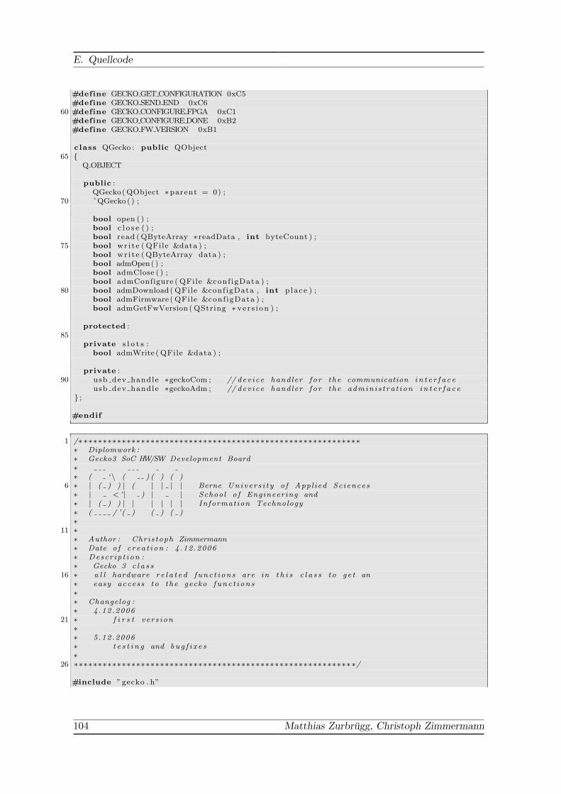
E. Quellcode
#define GECKO GET CONFIGURATION 0xC5#define GECKO SEND END 0xC6
60 #define GECKO CONFIGURE FPGA 0xC1#define GECKO CONFIGURE DONE 0xB2#define GECKO FW VERSION 0xB1
class QGecko : public QObject65 {
Q OBJECT
public :QGecko( QObject ∗parent = 0) ;
70 ˜QGecko ( ) ;
bool open ( ) ;bool c l o s e ( ) ;bool read (QByteArray ∗ readData , int byteCount ) ;
75 bool wr i t e ( QFile &data ) ;bool wr i t e (QByteArray data ) ;bool admOpen( ) ;bool admClose ( ) ;bool admConfigure ( QFile &conf igData ) ;
80 bool admDownload( QFile &configData , int p lace ) ;bool admFirmware ( QFile &conf igData ) ;bool admGetFwVersion ( QString ∗ ve r s i on ) ;
protected :85
private s l o t s :bool admWrite ( QFile &data ) ;
private :90 usb dev handle ∗geckoCom ; // dev i ce handler f o r the communication i n t e r f a c e
usb dev handle ∗geckoAdm ; // dev i ce handler f o r the admin i s t ra t ion i n t e r f a c e} ;
#endif
1 /∗ ∗∗∗∗∗∗∗∗∗∗∗∗∗∗∗∗∗∗∗∗∗∗∗∗∗∗∗∗∗∗∗∗∗∗∗∗∗∗∗∗∗∗∗∗∗∗∗∗∗∗∗∗∗∗∗∗∗∗∗ Diplomwork :∗ Gecko3 SoC HW/SW Development Board∗∗ ( ‘\ ( ) ( ) ( )
6 ∗ | ( ) ) | ( | | | | Berne Unive r s i t y o f Appl ied Sciences∗ | < ’| ) | | School o f Engineering and∗ | ( ) ) | | | | | | Information Technology∗ ( / ’( ) ( ) ( )∗
11 ∗∗ Author : Chris toph Zimmermann∗ Date o f c rea t i on : 4 .12.2006∗ Descr ip t ion :∗ Gecko 3 c l a s s
16 ∗ a l l hardware r e l a t e d func t i ons are in t h i s c l a s s to ge t an∗ easy access to the gecko func t i on s∗∗ Changelog :∗ 4.12.2006
21 ∗ f i r s t ver s ion∗∗ 5.12.2006∗ t e s t i n g and bu g f i x e s∗
26 ∗∗∗∗∗∗∗∗∗∗∗∗∗∗∗∗∗∗∗∗∗∗∗∗∗∗∗∗∗∗∗∗∗∗∗∗∗∗∗∗∗∗∗∗∗∗∗∗∗∗∗∗∗∗∗∗∗∗ ∗/
#include ”gecko . h”
104 Matthias Zurbrugg, Christoph Zimmermann

E.3. Hostsoftware
#include <iostream>31
QGecko : : QGecko( QObject ∗parent ): QObject ( parent )
{u s b i n i t ( ) ; // i n i t i a l i s i z e the l i b u s b
36 geckoAdm = 0 ;geckoCom = 0 ;
}
41 QGecko : : ˜ QGecko ( ){}
//−−−−−−−−−−−−−−−−−−−−−−−−−−−−−−−−−−−−−−−−−−−−−−−−−−−−−−−−−−−46 // func t i on s f o r normal communication with the gecko board
bool QGecko : : open ( ) {struct usb bus ∗ busses ;
u sb f i nd bu s s e s ( ) ;51 u s b f i n d d e v i c e s ( ) ; // rescan a l l usb t h in g s
busses = usb ge t bu s s e s ( ) ; // re turns the l i s t o f a l l usb busses
struct usb bus ∗bus ;56
for ( bus = busses ; bus ; bus = bus−>next ) {struct usb dev i c e ∗dev ;
for ( dev = bus−>dev i c e s ; dev ; dev = dev−>next ) { //go through a l l busses anda l l d e v i c e s and check i f i t i s a gecko
61 i f ( dev−>d e s c r i p t o r . idVendor == ID VENDOR GECKO3) {i f ( dev−>d e s c r i p t o r . idProduct == ID PRODUCT GECKO3) {
geckoCom = usb open ( dev ) ; //we found a gecko , now we open the dev i cechar dr name [ 1 0 0 ] ;int np = usb g e t d r i v e r np (geckoCom , 0 , dr name , 100) ; // checks i f t he re
i s a ke rne l d r i v e r loaded fo r t h i s dev i ce66 i f (np==0) {
u sb de t a ch ke rn e l d r i v e r np (geckoCom , 0) ; // unloads the ke rne l d r i v e ri f t he re i s one . e l s e the dev i ce i s not a v i a b l e f o r us
}int t = u sb c l a im i n t e r f a c e ( geckoCom , GECKO COM INTERFACE) ; //bound the
i n t e r f a c e from the os . now we can use t h i s i n t e r f a c ei f ( t == 0) {
71 return true ; //end of search ing f o r dev i c e s . the f i r s t founddev i ce i s used
}else {
return fa l se ;}
76 }}
}}return fa l se ;
81 }
bool QGecko : : c l o s e ( ){
i f ( geckoCom != 0) {86 u s b r e l e a s e i n t e r f a c e ( geckoCom , GECKO COM INTERFACE) ; // unr e g i s t e r the i n t e r f a c e
from the osu sb c l o s e ( geckoCom) ; // c l o s e the usb connect iongeckoCom = 0 ; // r e s e t s the dev i ce handler so we can de t e c t t ha t i t i s c l o s ed
Project Report 105

E. Quellcode
return true ;}
91 return fa l se ;}
bool QGecko : : read ( QByteArray ∗ readData , int byteCount ){
96 // reads data through the communication i n t e r f a c e from the fpgai f ( geckoCom != 0) {
char data [ 3 2 7 6 8 ] ;int r = usb bu lk read (geckoCom , GECKO COM EP READ, data , byteCount , 5000) ;i f ( r != 0) {
101 readData−>append (QByteArray ( data , byteCount ) ) ;return true ;
}}return fa l se ;
106 }
bool QGecko : : wr i t e ( QFile &data ) { // wr i t e s a whole f i l e through the communicationi n t e r f a c e to the fpga
i f ( geckoCom != 0) {bool loop = true ;
111 char targetArray [ 3 2 7 6 8 ] ;int t a r g e t S i z e = 0 ;
// the l i b u s b use an in t va lue as s i z e , so we must s p l i t the f i l e in to mu l t i p l et r an s f e r s
while ( loop == true ) {116 t a r g e t S i z e = data . read ( targetArray , 32768 ) ;
i f ( t a r g e t S i z e > 0) {int w = usb bu lk wr i t e ( geckoCom , GECKO COM EP WRITE, targetArray ,
t a r g e tS i z e , 5000) ;i f (w<=0){
return fa l se ;121 }
}else {
loop = fa l se ;}
126 }return true ;
}return fa l se ;
}131
bool QGecko : : wr i t e (QByteArray data ) { // wr i t e s a byteArray through the communicationi n t e r f a c e to the fpga
i f ( geckoCom != 0) {int w = usb bu lk wr i t e ( geckoCom , GECKO COM EP WRITE, data . data ( ) , data . s i z e ( ) ,
5000) ;i f (w>0){
136 return true ;}
}return fa l se ;
}141
//−−−−−−−−−−−−−−−−−−−−−−−−−−−−−−−−−−−−−−−−−−−−−−−−−−−−−−−−−−−// func t i on s f o r a l l the admin i s t r a t i v s t u f f :bool QGecko : : admOpen( ) {
//same th ing as QGecko : : open () only f o r the admin i s t ra t ion i n t e r f a c e146 struct usb bus ∗ busses ;
u sb f i nd bu s s e s ( ) ;u s b f i n d d e v i c e s ( ) ;
106 Matthias Zurbrugg, Christoph Zimmermann

E.3. Hostsoftware
151 busses = usb ge t bu s s e s ( ) ;
struct usb bus ∗bus ;
for ( bus = busses ; bus ; bus = bus−>next ) {156 struct usb dev i c e ∗dev ;
for ( dev = bus−>dev i c e s ; dev ; dev = dev−>next ) {i f ( dev−>d e s c r i p t o r . idVendor == ID VENDOR GECKO3) {
i f ( dev−>d e s c r i p t o r . idProduct == ID PRODUCT GECKO3) {161 geckoAdm = usb open ( dev ) ;
char dr name [ 1 0 0 ] ;int np = usb g e t d r i v e r np (geckoAdm , 0 , dr name , 100) ;i f (np==0) {
u sb de t a ch ke rn e l d r i v e r np (geckoAdm , 0) ;166 }
int t = u sb c l a im i n t e r f a c e (geckoAdm , GECKO ADM INTERFACE) ;i f ( t == 0) {
return true ; //end of search ing f o r dev i c e s . the f i r s t founddev i ce i s used
}171 else {
return fa l se ;}
}}
176 }}return fa l se ;
}
181 bool QGecko : : admClose ( ){
//same th ing as QGecko : : c l o s e () only f o r the admin i s t ra t ion i n t e r f a c ei f (geckoAdm != 0) {
u s b r e l e a s e i n t e r f a c e (geckoAdm , GECKO ADM INTERFACE) ;186 u sb c l o s e (geckoAdm) ;
geckoAdm = 0 ;return true ;
}return fa l se ;
191 }
bool QGecko : : admWrite ( QFile &data ) {//same th ing as QGecko : : wr i t e ( QFile &data ) only f o r the admin i s t ra t ion i n t e r f a c ei f (geckoAdm != 0) {
196 bool loop = true ;char targetArray [ 3 2 7 6 8 ] ;int t a r g e t S i z e = 0 ;
while ( loop == true ) {201 t a r g e t S i z e = data . read ( targetArray , 32768 ) ;
i f ( t a r g e t S i z e > 0) {int w = usb bu lk wr i t e (geckoAdm , GECKO ADM EP WRITE, targetArray ,
t a r g e tS i z e , 5000) ;i f (w<=0){
return fa l se ;206 }
}else {
loop = fa l se ;}
211 }return true ;
}
Project Report 107

E. Quellcode
return fa l se ;}
216bool QGecko : : admConfigure ( QFile &conf igData ) {
i f (geckoAdm != 0) {// send the vendor reque s t to s t a r t the fpga con f i gu ra t i onint b = usb contro l msg (geckoAdm , USB TYPE VENDOR, GECKO CONFIGURE FPGA, 0 , 0 ,
”” , 0 , 1000) ;221
i f (b>=0){// wr i t e s the b i t s t r eam in to the fpgai f ( admWrite ( conf igData ) ) {
char done [ 2 ] ;226 // checks i f the done s i g n a l from the fpga i s a s s e r t ed
int w = usb contro l msg (geckoAdm , USB TYPE VENDOR | USB ENDPOINT DIR MASK,GECKO CONFIGURE DONE, 0 , 0 , done , 1 , 1000) ;
i f (w>=0 && done [ 0 ] == char (GECKO CONFIGURE DONE) ) {return true ;
231 }}
}}return fa l se ;
236 }
bool QGecko : : admDownload( QFile &conf igData , int p lace ) {i f (geckoAdm != 0) {
// send the vendor reque s t to s t a r t the download o f a b i t s t r eam to the f l a s h ,i n c l ud ing the de s i r ed memory s l o t
241 int b = usb contro l msg (geckoAdm , USB TYPE VENDOR, GECKO SEND CONFIGURATION,place , 0 , ”” , 0 , 1000) ;
i f (b>=0){// wr i t e s the b i t s t r eam in to the sp i f l a s hi f ( admWrite ( conf igData ) ) {
// send the vendor reque s t to s i g n a l i s e the end o f the b i t s t r eam download246 int w = usb contro l msg (geckoAdm , USB TYPE VENDOR, GECKO SEND END, 0 , 0 , ”” ,
0 , 1000) ;i f (w>=0) {
return true ;}
}251 }
}return fa l se ;
}
256 bool QGecko : : admFirmware ( QFile &conf igData ) {i f (geckoAdm != 0) {
// send the vendor reque s t to s t a r t the download o f a cypress firmware f i l e ( inthe i i c format )
int b = usb contro l msg (geckoAdm , USB TYPE VENDOR, GECKO SEND FW, 0 , 0 , ”” , 0 ,1000) ;
i f (b>=0){261 // wr i t e s the b i t s t r eam in to the eeprom
i f ( admWrite ( conf igData ) ) {// send the vendor reque s t to s i g n a l i s e the end o f the firmware downloadint w = usb contro l msg (geckoAdm , USB TYPE VENDOR, GECKO SEND END, 0 , 0 , ”” ,
0 , 1000) ;i f (w>=0) {
266 return true ;}
}}
}271 return fa l se ;
108 Matthias Zurbrugg, Christoph Zimmermann

E.3. Hostsoftware
}
bool QGecko : : admGetFwVersion ( QString ∗ ve r s i on ) {i f (geckoAdm != 0) {
276 char fw [ 5 ] = ”” ;// send the vendor reque s t to r eque s t the firmware vers ion . the number i s in the
format X.XXint b = usb contro l msg (geckoAdm , USB TYPE VENDOR | USB ENDPOINT DIR MASK,
GECKO FW VERSION, 0 , 0 , fw , 4 , 1000) ;
i f (b>=0){281 //append the rece i v ed ver s ion to the passed QString
vers ion−>append (QByteArray ( fw , 4) ) ;return true ;
}}
286 return fa l se ;}
E.3.2. Gecko Administrator
/∗ ∗∗∗∗∗∗∗∗∗∗∗∗∗∗∗∗∗∗∗∗∗∗∗∗∗∗∗∗∗∗∗∗∗∗∗∗∗∗∗∗∗∗∗∗∗∗∗∗∗∗∗∗∗∗∗∗∗∗∗ Diplomwork :
3 ∗ Gecko3 SoC HW/SW Development Board∗∗ ( ‘\ ( ) ( ) ( )∗ | ( ) ) | ( | | | | Berne Unive r s i t y o f Appl ied Sciences∗ | < ’| ) | | School o f Engineering and
8 ∗ | ( ) ) | | | | | | Information Technology∗ ( / ’( ) ( ) ( )∗∗∗ Author : Chris toph Zimmermann
13 ∗ Date o f c rea t i on : 3 .12.2006∗ Descr ip t ion :∗ main f i l e o f the Gecko Administrator programm∗ accep t s the f o l l ow i n g command l i n e arguments :∗ −−f irmware shows the download firmware tab . d e f a u l t i t i s i n v i s i b l e
18 ∗∗ Changelog :∗ 3.12.2006∗ f i r s t ver s ion∗
23 ∗∗∗∗∗∗∗∗∗∗∗∗∗∗∗∗∗∗∗∗∗∗∗∗∗∗∗∗∗∗∗∗∗∗∗∗∗∗∗∗∗∗∗∗∗∗∗∗∗∗∗∗∗∗∗∗∗∗ ∗/
#include <qapp l i c a t i on . h>#include ”geckoadm . h”
28 int main ( int argc , char ∗∗ argv ) {QApplication a ( argc , argv ) ;geckoadm ∗ mw = new geckoadm ( ) ;mw−>show ( ) ;a . connect ( &a , SIGNAL( lastWindowClosed ( ) ) , &a , SLOT( qu i t ( ) ) ) ;
33 return a . exec ( ) ;}
1 /∗ ∗∗∗∗∗∗∗∗∗∗∗∗∗∗∗∗∗∗∗∗∗∗∗∗∗∗∗∗∗∗∗∗∗∗∗∗∗∗∗∗∗∗∗∗∗∗∗∗∗∗∗∗∗∗∗∗∗∗∗ Diplomwork :∗ Gecko3 SoC HW/SW Development Board∗∗ ( ‘\ ( ) ( ) ( )
6 ∗ | ( ) ) | ( | | | | Berne Unive r s i t y o f Appl ied Sciences∗ | < ’| ) | | School o f Engineering and
Project Report 109

E. Quellcode
∗ | ( ) ) | | | | | | Information Technology∗ ( / ’( ) ( ) ( )∗
11 ∗∗ Author : Chris toph Zimmermann∗ Date o f c rea t i on : 3 .12.2006∗ Descr ip t ion :∗ Header f i l e f o r the gecko 3 hos t so f tware
16 ∗∗ Changelog :∗ 3.12.2006∗ f i r s t ver s ion∗
21 ∗∗∗∗∗∗∗∗∗∗∗∗∗∗∗∗∗∗∗∗∗∗∗∗∗∗∗∗∗∗∗∗∗∗∗∗∗∗∗∗∗∗∗∗∗∗∗∗∗∗∗∗∗∗∗∗∗∗ ∗/
#ifndef SIMPLECOM H#define SIMPLECOM H
26 #include <iostream>
#include <QPushButton>#include <QTextEdit>#include <QFile>
31 #include <QFileDialog>#include <QApplication>#include <QVBoxLayout>#include <QHBoxLayout>#include <QWidget>
36 #include <QLineEdit>#include <QValidator>#include <QString>#include <QChar>#include <QFile>
41 #include <QByteArray>#include <QStatusBar>#include <QTabWidget>#include <QLabel>#include <QSize>
46 #include <QSpinBox>#include <QMessageBox>#include <QSettings>
#include ”gecko . h” //header f i l e o f the gecko c l a s s51
class QTextEdit ;
class geckoadm : public QWidget{
56 Q OBJECT
public :geckoadm (QWidget ∗parent = 0) ;˜geckoadm ( ) ;
61protected :
private s l o t s :void c loseEvent ( QCloseEvent ∗) ;
66 void c on f i gu r e ( ) ;void chooseConf igure ( ) ;void download ( ) ;void chooseDownload ( ) ;void f i rmware ( ) ;
71 void chooseFirmware ( ) ;void getFirmwareVersion ( ) ;
110 Matthias Zurbrugg, Christoph Zimmermann
E.3. Hostsoftware
private :QStr ingLi s t ∗arguments ;
76 QGecko ∗gecko ;QString ∗ conf igPath ;QString ∗downloadPath ;QString ∗ f irmwarePath ;QVBoxLayout ∗ layMain ;
81 QStatusBar ∗ s tatusBar ;QTabWidget ∗ tab ;QSize ∗ l i n eEd i t S i z e ;
QWidget ∗ tabConf igure ;86 QVBoxLayout ∗ l ayConf igure ;
QLineEdit ∗ l eCon f i gF i l e ;QPushButton ∗ btCon f i gF i l e ;QHBoxLayout ∗ layConfigFPGA ;QPushButton ∗btConfigFPGA ;
91QWidget ∗tabDownload ;QLineEdit ∗ l eDownloadFi le ;QPushButton ∗btDownloadFile ;QPushButton ∗btDownload ;
96 QHBoxLayout ∗ layDownloadButton ;QSpinBox ∗ s e l e c tCon f i g ;QLabel ∗ l a S e l e c tCon f i g ;QHBoxLayout ∗ l a yS e l e c tCon f i g ;QVBoxLayout ∗ layDownload ;
101
QWidget ∗ tabFirmware ;QLineEdit ∗ l eFirmwareVers ion ;QPushButton ∗btFirmwareVersion ;
106 QLabel ∗ laFirmwareVersion ;QLineEdit ∗ l eF i rmwareFi l e ;QPushButton ∗btFirmwareFi le ;QPushButton ∗btFirmware ;QHBoxLayout ∗ layFirmwareButton ;
111 QHBoxLayout ∗ layFirmwareVersion ;QVBoxLayout ∗ layFirmware ;
QWidget ∗ tabAbout ;QVBoxLayout ∗ layAbout ;
116 QHBoxLayout ∗ layHAbout ;QLabel ∗ laGecko ;QLabel ∗ l aVer s i on ;QLabel ∗ laDate ;QLabel ∗ l aDeve loper s ;
121 QLabel ∗ l aOrgan i sa t i on ;QLabel ∗ l aUr l ;
} ;
#endif
/∗ ∗∗∗∗∗∗∗∗∗∗∗∗∗∗∗∗∗∗∗∗∗∗∗∗∗∗∗∗∗∗∗∗∗∗∗∗∗∗∗∗∗∗∗∗∗∗∗∗∗∗∗∗∗∗∗∗∗∗∗ Diplomwork :∗ Gecko3 SoC HW/SW Development Board∗
5 ∗ ( ‘\ ( ) ( ) ( )∗ | ( ) ) | ( | | | | Berne Unive r s i t y o f Appl ied Sciences∗ | < ’| ) | | School o f Engineering and∗ | ( ) ) | | | | | | Information Technology∗ ( / ’( ) ( ) ( )
10 ∗∗∗ Author : Chris toph Zimmermann∗ Date o f c rea t i on : 20.11.2006
Project Report 111

E. Quellcode
∗ Descr ip t ion :15 ∗ Gecko 3 hos t so f tware . a l l admin i s t r a t i v e t a s k s o f the gecko board
∗ are usab l e with t h i s so f tware :∗ con f i gure the fpga∗ download fpga c o n f i g f i l e s to the onboard memory∗ download new ez−usb firmware
20 ∗∗ Changelog :∗ 3.12.2006∗ f i r s t vers ion , GUI implemented∗
25 ∗ 4.12.2006∗ usb func t i ons implemented∗ use o f QSet t ings to save informat ion fo r b e t t e r u s a b i l i t y∗∗ 5.12.2006
30 ∗ t e s t i n g and bu g f i x e s∗∗∗∗∗∗∗∗∗∗∗∗∗∗∗∗∗∗∗∗∗∗∗∗∗∗∗∗∗∗∗∗∗∗∗∗∗∗∗∗∗∗∗∗∗∗∗∗∗∗∗∗∗∗∗∗∗∗∗ ∗/
#include ”geckoadm . h”35
#define VERSION QString ( ” 0 .1 ” )#define DATE QString ( ” 3 . 12 . 2006 ” )#define DEVELOPERS QString ( ”Matthias Zurbrgg , Christoph Zimmermann” )#define ORGANISATION QString ( ”Berne Un ive r s i ty o f Applied Sc i ences , Microlab ” )
40 #define URL QString ( ”<a h r e f=\”http ://www. micro lab . ch\”>www. micro lab . ch</a>” )
geckoadm : : geckoadm (QWidget ∗parent ): QWidget ( parent )
{45 gecko = new QGecko ( ) ;
QSett ings : : setPath ( QSett ings : : IniFormat , QSett ings : : UserScope , 0) ;QCoreApplication : : setOrganizationName ( ”BFH Microlab ” ) ;QCoreApplication : : setOrganizationDomain ( ”micro lab . ch” ) ;
50 QCoreApplication : : setApplicationName ( ”Gecko 3 Administat ion Program” ) ;QSett ings s e t t i n g s ;i f ( s e t t i n g s . conta in s ( ” conf igPath ” ) ) {
conf igPath = new QString ( s e t t i n g s . va lue ( ” conf igPath ” ) . t oS t r i ng ( ) ) ;}
55 else {conf igPath = new QString ( ) ;
}i f ( s e t t i n g s . conta in s ( ”downloadPath” ) ) {
downloadPath = new QString ( s e t t i n g s . va lue ( ”downloadPath” ) . t oS t r i ng ( ) ) ;60 }
else {downloadPath = new QString ( ) ;
}i f ( s e t t i n g s . conta in s ( ” firmwarePath” ) ) {
65 firmwarePath = new QString ( s e t t i n g s . va lue ( ” firmwarePath” ) . t oS t r i ng ( ) ) ;}else {
f irmwarePath = new QString ( ) ;}
70// crea t e the con f i gure FPGA tabtabConf igure = new QWidget ( ) ;l eCon f i gF i l e = new QLineEdit ( ) ;l eCon f i gF i l e−>setReadOnly ( true ) ;
75 l eCon f i gF i l e−>setText (∗ conf igPath ) ;l eCon f i gF i l e−>setMinimumSize ( QSize ( 100 ,
QFontMetrics ( l eCon f i gF i l e−>f on t ( ) ) . he ight ( ) ) ) ;b tCon f i gF i l e = new QPushButton ( t r ( ” S e l e c t c o n f i g f i l e ” ) ) ;connect ( btConf igF i l e , SIGNAL( c l i c k e d ( ) ) , this , SLOT( chooseConf igure ( ) ) ) ;
112 Matthias Zurbrugg, Christoph Zimmermann

E.3. Hostsoftware
btConfigFPGA = new QPushButton ( t r ( ”Conf igure FPGA” ) ) ;80 btConfigFPGA−>s e tF ix edS i z e ( 140 , 50 ) ;
connect (btConfigFPGA , SIGNAL( c l i c k e d ( ) ) , this , SLOT( con f i gu r e ( ) ) ) ;
layConfigFPGA = new QHBoxLayout ( ) ;layConfigFPGA−>addWidget ( btConfigFPGA) ;
85layConf igure = new QVBoxLayout ( ) ;layConf igure−>addWidget ( b tCon f i gF i l e ) ;layConf igure−>addWidget ( l eCon f i gF i l e ) ;layConf igure−>addLayout ( layConfigFPGA) ;
90 tabConf igure−>setLayout ( layConf igure ) ;
// crea t e the download con f i gu ra t i on tabtabDownload = new QWidget ( ) ;leDownloadFi le = new QLineEdit ( ) ;
95 leDownloadFile−>setReadOnly ( true ) ;leDownloadFile−>setText (∗ downloadPath ) ;leDownloadFile−>setMinimumSize ( QSize ( 100 ,
QFontMetrics ( leDownloadFile−>f on t ( ) ) . he ight ( ) ) ) ;btDownloadFile = new QPushButton ( t r ( ” S e l e c t c o n f i g f i l e ” ) ) ;connect ( btDownloadFile , SIGNAL( c l i c k e d ( ) ) , this , SLOT( chooseDownload ( ) ) ) ;
100 btDownload = new QPushButton ( t r ( ”Download” ) ) ;btDownload−>s e tF ix edS i z e ( 140 , 50 ) ;connect ( btDownload , SIGNAL( c l i c k e d ( ) ) , this , SLOT( download ( ) ) ) ;
layDownloadButton = new QHBoxLayout ( ) ;105 layDownloadButton−>addWidget ( btDownload ) ;
s e l e c tCon f i g = new QSpinBox ( ) ;s e l e c tCon f i g−>setRange (0 , GECKO MAX CONFIGS−1) ;s e l e c tCon f i g−>s e tF ix edS i z e ( QSize ( 40 ,
2∗QFontMetrics ( leDownloadFile−>f on t ( ) ) . he ight ( ) ) ) ;110 l aS e l e c tCon f i g = new QLabel ( t r ( ”Choose c o n f i g f i l e t a r g e t memory : ” ) ) ;
l a ySe l e c tCon f i g = new QHBoxLayout ( ) ;l aySe l e c tCon f i g−>addWidget ( l a S e l e c tCon f i g ) ;l aySe l e c tCon f i g−>addWidget ( s e l e c tCon f i g ) ;
115 layDownload = new QVBoxLayout ( ) ;layDownload−>addWidget ( btDownloadFile ) ;layDownload−>addWidget ( leDownloadFi le ) ;layDownload−>addLayout ( l a ySe l e c tCon f i g ) ;layDownload−>addLayout ( layDownloadButton ) ;
120 tabDownload−>setLayout ( layDownload ) ;
// crea t e the download firmware tabtabFirmware = new QWidget ( ) ;laFirmwareVersion = new QLabel ( t r ( ”Current f irmware ve r s i on : ” ) ) ;
125 leFirmwareVers ion = new QLineEdit ( ) ;leFirmwareVersion−>setReadOnly ( true ) ;leFirmwareVersion−>s e tF ix edS i z e ( QSize ( 60 ,
QFontMetrics ( leFirmwareVersion−>f on t ( ) ) . he ight ( ) ) ) ;btFirmwareVersion = new QPushButton ( t r ( ”Get f irmware ve r s i on ” ) ) ;connect ( btFirmwareVersion , SIGNAL( c l i c k e d ( ) ) , this , SLOT( getFirmwareVersion ( ) ) ) ;
130layFirmwareVersion = new QHBoxLayout ( ) ;layFirmwareVersion−>addWidget ( laFirmwareVersion ) ;layFirmwareVersion−>addWidget ( leFirmwareVers ion ) ;
135 leFi rmwareFi l e = new QLineEdit ( ) ;l eFirmwareFi le−>setReadOnly ( true ) ;l eFirmwareFi le−>setText (∗ f irmwarePath ) ;leFirmwareFi le−>setMinimumSize ( QSize ( 100 ,
QFontMetrics ( leFirmwareFi le−>f on t ( ) ) . he ight ( ) ) ) ;btFirmwareFi le = new QPushButton ( t r ( ” S e l e c t f irmware f i l e ” ) ) ;
140 connect ( btFirmwareFile , SIGNAL( c l i c k e d ( ) ) , this , SLOT( chooseFirmware ( ) ) ) ;
Project Report 113

E. Quellcode
btFirmware = new QPushButton ( t r ( ”Download firmware ” ) ) ;btFirmware−>s e tF ix edS i z e ( 140 , 50 ) ;connect ( btFirmware , SIGNAL( c l i c k e d ( ) ) , this , SLOT( firmware ( ) ) ) ;
145 layFirmwareButton = new QHBoxLayout ( ) ;layFirmwareButton−>addWidget ( btFirmware ) ;
layFirmware = new QVBoxLayout ( ) ;layFirmware−>addWidget ( btFirmwareVersion ) ;
150 layFirmware−>addLayout ( layFirmwareVersion ) ;layFirmware−>addWidget ( btFirmwareFi le ) ;layFirmware−>addWidget ( l eF i rmwareFi l e ) ;layFirmware−>addLayout ( layFirmwareButton ) ;tabFirmware−>setLayout ( layFirmware ) ;
155// crea t e the about tabtabAbout = new QWidget ( ) ;laGecko = new QLabel ( t r ( ”Gecko 3 Administrat ion Program” ) ) ;l aVer s i on = new QLabel ( t r ( ”Vers ion : ” ) + VERSION) ;
160 laDate = new QLabel ( t r ( ”Date : ” ) + DATE) ;l aDeve loper s = new QLabel (DEVELOPERS) ;l aOrgan i sa t i on = new QLabel (ORGANISATION) ;l aUr l = new QLabel (URL) ;layAbout = new QVBoxLayout ( ) ;
165 layAbout−>addWidget ( laGecko ) ;layAbout−>addWidget ( l aVer s i on ) ;layAbout−>addWidget ( laDate ) ;layAbout−>addWidget ( l aDeve loper s ) ;layAbout−>addWidget ( l aOrgan i sa t i on ) ;
170 layAbout−>addWidget ( l aUr l ) ;layHAbout = new QHBoxLayout ( ) ;layHAbout−>addLayout ( layAbout ) ;tabAbout−>setLayout ( layHAbout ) ;
175 // crea t e the s t a t u s bars tatusBar = new QStatusBar ( ) ;statusBar−>setS izeGr ipEnabled ( fa l se ) ;statusBar−>showMessage ( t r ( ”Ready” ) ) ;
180 //add anything t o ghe t e r in the tab stab = new QTabWidget ( ) ;tab−>addTab( tabConf igure , t r ( ”Conf igure FPGA” ) ) ;tab−>addTab( tabDownload , t r ( ”Download Con f i gu ra t i ons ” ) ) ;tab−>addTab( tabFirmware , t r ( ”Download Firmware” ) ) ;
185 tab−>addTab( tabAbout , t r ( ”About” ) ) ;
// crea t e the main windowlayMain = new QVBoxLayout ( ) ;layMain−>addWidget ( tab ) ;
190 layMain−>addWidget ( statusBar ) ;setLayout ( layMain ) ;setWindowTitle ( t r ( ”Gecko 3 Administrator ” ) ) ;se tFixedHeight (260) ;r e s i z e ( 450 , 260 ) ;
195 }
geckoadm : : ˜ geckoadm ( ){}
200void geckoadm : : c loseEvent ( QCloseEvent ∗){
QSett ings s e t t i n g s ;s e t t i n g s . setValue ( ” conf igPath ” , ∗ conf igPath ) ;
205 s e t t i n g s . setValue ( ”downloadPath” , ∗downloadPath ) ;s e t t i n g s . setValue ( ” firmwarePath” , ∗ f irmwarePath ) ;
114 Matthias Zurbrugg, Christoph Zimmermann
E.3. Hostsoftware
}
void geckoadm : : c on f i gu r e ( )210 {
i f ( ! conf igPath−>isEmpty ( ) ) {bool t = gecko−>admOpen( ) ;i f ( t == true ) {
statusBar−>showMessage ( t r ( ”Device found and ready” ) ) ;215 QFile f ( ∗ conf igPath ) ;
i f ( ! f . open (QIODevice : : ReadOnly ) ) {statusBar−>showMessage ( t r ( ”Error : F i l e could not be opend” ) ) ;return ;
}220
bool s t a t e = gecko−>admConfigure ( f ) ;i f ( s t a t e ) {
statusBar−>showMessage ( t r ( ”FPGA s u c c e s s f u l l y con f i gu r ed ” ) ) ;}
225 else {statusBar−>showMessage ( t r ( ”Error : FPGA could not be con f i gu r ed . Check the
FPGA type” ) ) ;}
f . c l o s e ( ) ;230 gecko−>admClose ( ) ;
}else {
statusBar−>showMessage ( t r ( ”Error : No Gecko found . Please check the USBconnect ion ” ) ) ;
}235 }
else {QMessageBox : : warning ( this , t r ( ”No f i l e s e l e c t e d ” ) , t r ( ”You have to s e l e c t a F i l e
be f o r e you can con f i gu r e the FPGA” ) , QMessageBox : : Ok, QMessageBox : : NoButton ) ;}
}240
void geckoadm : : chooseConf igure ( ){
∗ conf igPath = QFileDia log : : getOpenFileName ( this , t r ( ”Choose FPGA con f i g F i l e ” ) ,∗ conf igPath , ” X i l i nx Bin F i l e s ( ∗ . bin ) ” ) ;
l eCon f i gF i l e−>setText (∗ conf igPath ) ;245 }
void geckoadm : : download ( ){
i f ( ! downloadPath−>isEmpty ( ) ) {250 bool t = gecko−>admOpen( ) ;
i f ( t == true ) {statusBar−>showMessage ( t r ( ”Device found and ready” ) ) ;QFile f ( ∗downloadPath ) ;i f ( ! f . open (QIODevice : : ReadOnly ) ) {
255 statusBar−>showMessage ( t r ( ”Error : F i l e could not be opend” ) ) ;return ;
}
bool s t a t e = gecko−>admDownload( f , s e l e c tCon f i g−>value ( ) ) ;260 i f ( s t a t e ) {
statusBar−>showMessage ( t r ( ” Conf igurat ion s u c c e s s f u l l y downloaded” ) ) ;}else {
statusBar−>showMessage ( t r ( ”Error : Conf igurat ion not downloaded” ) ) ;265 }
f . c l o s e ( ) ;gecko−>admClose ( ) ;
Project Report 115

E. Quellcode
}270 else {
statusBar−>showMessage ( t r ( ”Error : No Gecko found . Please check the USBconnect ion ” ) ) ;
}}else {
275 QMessageBox : : warning ( this , t r ( ”No f i l e s e l e c t e d ” ) , t r ( ”You have to s e l e c t a F i l ebe f o r e you can con f i gu r e the FPGA” ) , QMessageBox : : Ok, QMessageBox : : NoButton ) ;
}}
void geckoadm : : chooseDownload ( )280 {
∗downloadPath = QFileDia log : : getOpenFileName ( this , t r ( ”Choose FPGA con f i g F i l e ” ) ,∗downloadPath , ” X i l i nx Bin F i l e s ( ∗ . bin ) ” ) ;
leDownloadFile−>setText (∗ downloadPath ) ;}
285 void geckoadm : : f irmware ( ){
i f ( ! firmwarePath−>isEmpty ( ) ) {bool t = gecko−>admOpen( ) ;i f ( t == true ) {
290 statusBar−>showMessage ( t r ( ”Device found and ready” ) ) ;QFile f ( ∗ f irmwarePath ) ;i f ( ! f . open (QIODevice : : ReadOnly ) ) {
statusBar−>showMessage ( t r ( ”Error : F i l e could not be opend” ) ) ;return ;
295 }
bool s t a t e = gecko−>admFirmware ( f ) ;i f ( s t a t e ) {
statusBar−>showMessage ( t r ( ”Firmware s u c c e s s f u l l y downloaded” ) ) ;300 }
else {statusBar−>showMessage ( t r ( ”Error : Firmware not downloaded” ) ) ;
}
305 f . c l o s e ( ) ;gecko−>admClose ( ) ;
}else {
statusBar−>showMessage ( t r ( ”Error : No Gecko found . Please check the USBconnect ion ” ) ) ;
310 }}else {
QMessageBox : : warning ( this , t r ( ”No f i l e s e l e c t e d ” ) , t r ( ”You have to s e l e c t aF i rmware f i l e b e f o r e you can download i t ” ) , QMessageBox : : Ok,QMessageBox : : NoButton ) ;
}315 }
void geckoadm : : chooseFirmware ( ){
∗ f irmwarePath = QFileDia log : : getOpenFileName ( this , t r ( ”Choose Cypress FirmwareF i l e ” ) , ∗ firmwarePath , ”Cypress Firmware F i l e ( ∗ . i i c ) ” ) ;
320 leFirmwareFi le−>setText (∗ f irmwarePath ) ;}
void geckoadm : : getFirmwareVersion ( ){
325 bool t = gecko−>admOpen( ) ;i f ( t == true ) {
statusBar−>showMessage ( t r ( ”Device found and ready” ) ) ;
116 Matthias Zurbrugg, Christoph Zimmermann

E.3. Hostsoftware
QString ∗ ve r s i on = new QString ( ) ;bool s t a t e = gecko−>admGetFwVersion ( ve r s i on ) ;
330 i f ( s t a t e ) {leFirmwareVersion−>setText (∗ ve r s i on ) ;statusBar−>showMessage ( t r ( ”Firmwarevers ion s u c c e s s f u l l y read ” ) ) ;
}else {
335 statusBar−>showMessage ( t r ( ”Error : Firmwarevers ion could not be read ” ) ) ;}
gecko−>admClose ( ) ;}
340 else {statusBar−>showMessage ( t r ( ”Error : No Gecko found . Please check the USB
connect ion ” ) ) ;}
}
E.3.3. Simplecom
/∗ ∗∗∗∗∗∗∗∗∗∗∗∗∗∗∗∗∗∗∗∗∗∗∗∗∗∗∗∗∗∗∗∗∗∗∗∗∗∗∗∗∗∗∗∗∗∗∗∗∗∗∗∗∗∗∗∗∗∗2 ∗ Diplomwork :
∗ Gecko3 SoC HW/SW Development Board∗∗ ( ‘\ ( ) ( ) ( )∗ | ( ) ) | ( | | | | Berne Unive r s i t y o f Appl ied Sciences
7 ∗ | < ’| ) | | School o f Engineering and∗ | ( ) ) | | | | | | Information Technology∗ ( / ’( ) ( ) ( )∗∗
12 ∗ Author : Chris toph Zimmermann∗ Date o f c rea t i on : 20.11.2006∗ Descr ip t ion :∗∗
17 ∗ Changelog :∗ 29.11.2006∗ f i r s t ver s ion∗∗ 5.12.2006
22 ∗ new vers ion tha t use the QGecko c l a s s to show how easy you can∗ implement a own communication so f tware∗∗∗∗∗∗∗∗∗∗∗∗∗∗∗∗∗∗∗∗∗∗∗∗∗∗∗∗∗∗∗∗∗∗∗∗∗∗∗∗∗∗∗∗∗∗∗∗∗∗∗∗∗∗∗∗∗∗∗ ∗/
27 #ifndef SIMPLECOM H#define SIMPLECOM H
#include <iostream>
32 #include <QPushButton>#include <QTextEdit>#include <QFile>#include <QFileDialog>#include <QApplication>
37 #include <QVBoxLayout>#include <QWidget>#include <QLineEdit>#include <QValidator>#include <QString>
42 #include <QChar>#include <QFile>#include <QByteArray>
Project Report 117

E. Quellcode
#include ”gecko . h”47
class QTextEdit ;
class simplecom : public QWidget{
52 Q OBJECT
public :simplecom (QWidget ∗parent = 0) ;˜ simplecom ( ) ;
57protected :
private s l o t s :void c loseEvent ( QCloseEvent ∗) ;
62 void send ( ) ;void r e c e i v e ( ) ;bool geckoConnect ( ) ;QString toHex (QByteArray data ) ;uchar nibbleToHex ( uchar va lue ) ;
67private :
QTextEdit ∗e ;QPushButton ∗ f i l eOpen ;
QPushButton ∗ rece iveData ;72 QLineEdit ∗numberInput ;
QVBoxLayout ∗ l ayout ;QGecko ∗gecko ;QString path ;
} ;77
#endif
/∗ ∗∗∗∗∗∗∗∗∗∗∗∗∗∗∗∗∗∗∗∗∗∗∗∗∗∗∗∗∗∗∗∗∗∗∗∗∗∗∗∗∗∗∗∗∗∗∗∗∗∗∗∗∗∗∗∗∗∗2 ∗ Diplomwork :
∗ Gecko3 SoC HW/SW Development Board∗∗ ( ‘\ ( ) ( ) ( )∗ | ( ) ) | ( | | | | Berne Unive r s i t y o f Appl ied Sciences
7 ∗ | < ’| ) | | School o f Engineering and∗ | ( ) ) | | | | | | Information Technology∗ ( / ’( ) ( ) ( )∗∗
12 ∗ Author : Chris toph Zimmermann∗ Date o f c rea t i on : 20.11.2006∗ Descr ip t ion :∗∗
17 ∗ Changelog :∗ 29.11.2006∗ f i r s t ver s ion∗∗∗∗∗∗∗∗∗∗∗∗∗∗∗∗∗∗∗∗∗∗∗∗∗∗∗∗∗∗∗∗∗∗∗∗∗∗∗∗∗∗∗∗∗∗∗∗∗∗∗∗∗∗∗∗∗∗∗ ∗/
22#include ” simplecom . h”
simplecom : : simplecom (QWidget ∗parent ): QWidget ( parent )
27 {gecko = new QGecko ( ) ;
QString path = QString : : nu l l ;
118 Matthias Zurbrugg, Christoph Zimmermann

E.3. Hostsoftware
32 f i l eOpen = new QPushButton ( ) ;connect ( f i l eOpen , SIGNAL( c l i c k e d ( ) ) , this , SLOT( send ( ) ) ) ;f i l eOpen−>setText ( t r ( ”Send F i l e ” ) ) ;
r ece iveData = new QPushButton ( ) ;37 connect ( rece iveData , SIGNAL( c l i c k e d ( ) ) , this , SLOT( r e c e i v e ( ) ) ) ;
rece iveData−>setText ( t r ( ”Read Data” ) ) ;
numberInput = new QLineEdit ( ) ;numberInput−>s e tVa l i da t o r (new QIntVal idator ( 0 , 3000 , this ) ) ;
42 connect ( numberInput , SIGNAL( re turnPres sed ( ) ) , this , SLOT( r e c e i v e ( ) ) ) ;
e = new QTextEdit ( ) ;e−>setReadOnly ( true ) ;
47 layout = new QVBoxLayout ;setLayout ( layout ) ;layout−>addWidget ( f i l eOpen ) ;layout−>addWidget ( rece iveData ) ;layout−>addWidget ( numberInput ) ;
52 layout−>addWidget ( e ) ;
r e s i z e ( 450 , 600 ) ;//geckoConnect ( ) ;
}57
simplecom : : ˜ simplecom ( ){}
62void simplecom : : c lo seEvent ( QCloseEvent ∗){
//gecko−>c l o s e () ;}
67void simplecom : : send ( ){
i f ( geckoConnect ( ) == true ) {QString f i leName = QFileDia log : : getOpenFileName ( this , QString : : nu l l , path ) ;
72 path = fi leName ;
i f ( ! f i leName . isEmpty ( ) ) {
QFile f ( f i leName ) ;77 i f ( ! f . open (QIODevice : : ReadOnly ) ) {
e−>append ( t r ( ”Error opening f i l e ” ) ) ;return ;
}i f ( gecko−>wr i t e ( f ) ) {
82 f . r e s e t ( ) ;QByteArray data = f . r eadAl l ( ) ;e−>append ( t r ( ”Sent Data:<br>” ) + toHex ( data ) ) ;
}// QByteArray data = f . readAl l ( ) ;
87 // i f ( gecko−>wr i t e ( data ) ) {// e−>append ( t r (” Sent Data:<br >”) + toHex ( data ) ) ;// }
else {e−>append ( t r ( ”Error sending data” ) ) ;
92 }f . c l o s e ( ) ;gecko−>c l o s e ( ) ;
}}
97 else
Project Report 119

E. Quellcode
{e−>append ( t r ( ”No dev i c e connected . Can ’ t send f i l e ” ) ) ;
}}
102void simplecom : : r e c e i v e ( ){
i f ( geckoConnect ( ) == true ) {bool ok ;
107 int number = numberInput−>t ex t ( ) . t o In t (&ok ) ;
i f ( ok == true ) {QByteArray ∗ bla = new QByteArray ( ) ;
112 bool t = gecko−>read ( bla , number ) ;i f ( t ) {
QString r e c e i v ed = QString ( toHex (∗ bla ) ) ;e−>append ( t r ( ”Received Data : ” ) + r e c e i v ed ) ;
}117 else {
e−>append ( t r ( ”Error read ing data” ) ) ;}
}else {
122 e−>append ( t r ( ” Please ente r the number o f bytes to read ” ) ) ;}
}else{
127 e−>append ( t r ( ”No dev i c e connected . Can ’ t r e c e i v e data” ) ) ;}gecko−>c l o s e ( ) ;
}
132 bool simplecom : : geckoConnect ( ){
int t = gecko−>open ( ) ;i f ( t == true ) {
e−>append ( t r ( ”Device found and ready” ) ) ;137 return true ;
}else {
e−>append ( t r ( ”Error opening the Device ” ) ) ;return fa l se ;
142 }}
QString simplecom : : toHex (QByteArray data ) {QString ∗ s t r i n g = new QString ( ”” ) ;
147for ( int i = 0 ; i < data . s i z e ( ) −1; i++) {
s t r i ng−>append ( ”0x” ) ;uchar va lue = uchar ( data . at ( i ) ) ;s t r i ng−>append (QChar( nibbleToHex ( ( value >>4)& 0x0F) ) ) ;
152 s t r i ng−>append (QChar( nibbleToHex ( value & 0x0F) ) ) ;s t r i ng−>append ( ” , ” ) ;
}s t r i ng−>append ( ”0x” ) ;uchar va lue = uchar ( data . at ( data . s i z e ( ) ) ) ;
157 s t r i ng−>append (QChar( nibbleToHex ( ( value >>4)& 0x0F) ) ) ;s t r i ng−>append (QChar( nibbleToHex ( value & 0x0F) ) ) ;
return ∗ s t r i n g ;}
162uchar simplecom : : nibbleToHex ( uchar va lue ) {
120 Matthias Zurbrugg, Christoph Zimmermann

E.3. Hostsoftware
uchar hex = ’X ’ ;switch ( va lue ) {
case 0 : hex = ’ 0 ’ ;167 break ;
case 1 : hex = ’ 1 ’ ;break ;case 2 : hex = ’ 2 ’ ;break ;
172 case 3 : hex = ’ 3 ’ ;break ;case 4 : hex = ’ 4 ’ ;break ;case 5 : hex = ’ 5 ’ ;
177 break ;case 6 : hex = ’ 6 ’ ;break ;case 7 : hex = ’ 7 ’ ;break ;
182 case 8 : hex = ’ 8 ’ ;break ;case 9 : hex = ’ 9 ’ ;break ;case 10 : hex = ’A ’ ;
187 break ;case 11 : hex = ’B ’ ;break ;case 12 : hex = ’C ’ ;break ;
192 case 13 : hex = ’D’ ;break ;case 14 : hex = ’E ’ ;break ;case 15 : hex = ’F ’ ;
197 break ;default : hex = ’X ’ ;
}return hex ;
}
Project Report 121

F. Schemas
F.1. Gecko 3, Stand 9. Dezember 2006
122 Christoph Zimmermann

F.1. Gecko 3, Stand 9. Dezember 2006
11
22
33
44
55
66
77
88
DD
CC
BB
AA
pow
erpo
wer
.SC
HD
OC
PWR
_DO
WN
/IN
TE
TH_R
ESE
T
Flas
h_D
1_[0
..15]
Power GoodLow Battery
Flas
h_D
0_[0
..15]
Flas
h_B
YTE
Flas
h_W
EFl
ash_
RP
Flas
h_O
EFl
ash_
CE
0
SDA_extSCL_ext
nOEnWE
RDnWR
nCS4nCS3nCS1
RDY
PWM[0..7]
GPIO1_[0..59]
Encoder[0..7]Sensors[0..5]
GPIO2[0..34]
Flas
h_A
[0..2
3]
DREQ[1..2]
MD[0..31]MA[0..25]
DQM[0..3]
MOSISCLK
MISOSPI_CS_F
Dra
m_D
1_[0
..15]
Dra
m_A
1_[0
..13]
Dra
m_L
DM
1D
ram
_UD
M1
Dra
m_C
S1D
ram
_WE1
Dra
m_C
AS1
Dra
m_R
AS1
Dra
m_C
KE1
Dra
m_C
K1
Dra
m_C
K1
Dra
m_B
A1_
1D
ram
_BA
1_0
Dra
m_L
DQ
S1D
ram
_UD
QS1
LED
[0..7
]
But
ton[
0..2
]Sw
itch[
0..3
]
TX
_CLK
RX
D_[
0..3
]
RX
_CL
KR
X_D
VR
X_E
R
CR
SC
OL
TX
_EN
TX
D_[
0..3
]
MD
CM
DIO
D[0
..15]
DO
NE
INIT
_B/W
RX
PRO
G_B
RD
WR
_B/W
RU
BU
SY/R
DY
X
CS_
B/R
DY
U
CC
LK
Dra
m_D
0_[0
..15]
Dra
m_A
0_[0
..13]
Dra
m_L
DM
0D
ram
_UD
M0
Dra
m_C
S0D
ram
_WE0
Dra
m_C
AS0
Dra
m_R
AS0
Dra
m_C
KE0
Dra
m_C
K0
Dra
m_C
K0
Dra
m_B
A0_
1D
ram
_BA
0_0
Dra
m_L
DQ
S0D
ram
_UD
QS0
EXTCLK0EXTCLK1
TCKTDI
TMSTDO
Serial outSerial in
Reset
fpga
fpga
.SC
HD
OC
Flas
h_D
Q[0
..15]
Flas
h_A
[0..2
3]
Flas
h_B
YTE
Flas
h_W
EFl
ash_
RP
Flas
h_O
EFl
ash_
CE
0
FL flas
h.Sc
hDoc
1
Ber
ne S
choo
l of A
pplie
d S
cien
ce
Sch
ool o
f Eng
inee
ring
and
Info
rmat
ion
Tech
nolo
gyQ
uellg
asse
21
CH
-250
1 Bi
el18
Gec
ko3:
So
C D
evel
opm
ent
Plat
form
0.7
08.1
2.20
0615
:21:
29C
:\Doc
umen
ts a
nd S
ettin
gs\z
imm
c5\s
vn\to
p.Sc
hDoc
Tite
l
Bla
ttgrö
sse:
Num
mer
:
Dat
um:
Dat
ei:
Rev
isio
n:
Bla
ttvo
nZe
it:
A3
Dra
m_D
Q[0
..15]
Dra
m_A
[0..1
3]
Dra
m_L
DM
Dra
m_U
DM
Dra
m_C
SD
ram
_WE
Dra
m_C
AS
Dra
m_R
AS
Dra
m_C
KE
Dra
m_C
KD
ram
_CK
Dra
m_B
A1
Dra
m_B
A0
Dra
m_L
DQ
SD
ram
_UD
QS
RA
Mdr
am.S
CH
DO
C
MO
SI
SPI_
CS_
F
SCL
K
MIS
O
spi-
flash
spi-
flash
.Sch
Doc
PWR
_DO
WN
/IN
TE
TH_R
ESE
T
TX
_CLK
RX
D_[
0..3
]
RX
_CL
KR
X_D
VR
X_E
R
CR
SC
OL
TX
_EN
TX
D_[
0..3
]
MD
CM
DIO
ethe
rnet
ethe
rnet
.SC
HD
OC
D[0
..15]
Vbu
s
DO
NE
INIT
_B/W
RX
PRO
G_B
RD
WR
_B/W
RU
BU
SY/R
DY
X
RE
SET
CS_
B/R
DY
U
CC
LK
MIS
OSP
I_C
S_F
MO
SISC
LK
SDA
SCL
Vbu
s_sw
usb
usb.
SCH
DO
C
Dra
m_D
1_[0
..15]
Dra
m_A
1_[0
..13]
Dra
m_A
0_[0
..13]
Dra
m_D
0_[0
..15]
Dra
m_D
Q[0
..15]
Dra
m_A
[0..1
3]
Dra
m_L
DM
Dra
m_U
DM
Dra
m_C
SD
ram
_WE
Dra
m_C
AS
Dra
m_R
AS
Dra
m_C
KE
Dra
m_C
KD
ram
_CK
Dra
m_B
A1
Dra
m_B
A0
Dra
m_L
DQ
SD
ram
_UD
QS
RA
Mdr
am.S
CH
DO
C
Flas
h_D
Q[0
..15]
Flas
h_A
[0..2
3]
Flas
h_B
YTE
Flas
h_W
EFl
ash_
RP
Flas
h_O
EFl
ash_
CE
0
FL flas
h.Sc
hDoc
TCKTDI
TMSTDO
Serial outSerial in
jtag
jtag.
SchD
oc
SDA
SCL
Vbu
s_sw
i2c
i2c.
SchD
oc
Vbus
PWM[0..7]
GPIO1_[0..59]
Encoder[0..7]Sensors[0..5]
Power GoodLow Battery
io-b
usio
-bus
.Sch
Doc
SDA_ext
DREQ[1..2]
Reset
MD[0..31]
GPIO2[0..34]
MA[0..25]
DQM[0..3]
SCL_ext
nOEnWE
RDnWR
nCS4nCS3nCS1
RDY
EXTCLK0EXTCLK1
io-b
us2
io-b
us2.
SchD
oc
LED
[0..7
]
But
ton[
0..2
]Sw
itch[
0..3
]
Res
et
switc
hes
switc
hes.S
chD
oc
Flas
h_A
[0..2
3]
Abbildung F.1.: Blockdiagramm
Project Report 123

F. Schemas
11
22
33
44
55
66
77
88
DD
CC
BB
AA
PWR
_DO
WN
/IN
T
ETH
_RE
SET
Flas
h_D
0_[0
..15]
Pow
er G
ood
Low
Bat
tery
Flas
h_D
1_[0
..15]
Flas
h_B
YTE
Flas
h_W
E
Flas
h_R
P
Flas
h_O
E
Flas
h_C
E0
SDA
SCL
SSPS
CL
K
SSPS
FRM
SSPT
XD
SSPR
XD
nOE
nWE
RD
nWR
nCS4
nCS3
nCS1
RD
Y
FF_R
XD
FF_C
TS
FF_D
CD
FF_D
SR
FF_R
I
FF_R
TS
FF_D
TR
FF_T
XD
PWM
[0..7
]
GPI
O1_
[0..5
]
Enc
oder
[0..7
]
Sens
ors[
0..5
]
1-H
z-C
lock
SSPE
XT
CLK
SSPS
YSC
LK
GPI
O2[
0..1
8]
Flas
h_A
[0..2
3]
DR
EQ[1
..2]
MD
[0..3
1]
MA
[0..2
5]
DQ
M[0
..3]
MO
SI
SCL
K
MIS
O
SPI_
CS_
F
LED
[0..7
]
But
ton[
0..3
]
Switc
h[0.
.3]
TX
_CLK
RX
D_[
0..3
]
RX
_CL
K
RX
_DV
RX
_ER
CR
S
CO
L
TX
_EN
TX
D_[
0..3
]
MD
C
MD
IO
D[0
..15]
DO
NE
INIT
_B/W
RX
PRO
G_B
RD
WR
_B/W
RU
BU
SY/R
DY
X
PKTE
ND
CS_
B/R
DY
U
CC
LK
2
Ber
ne S
choo
l of A
pplie
d S
cien
ce
Sch
ool o
f Eng
inee
ring
and
Info
rmat
ion
Tech
nolo
gyQ
uellg
asse
21
CH
-250
1 Bi
el18
Gec
ko3:
FP
GA
Par
ts
0.7
08.1
2.20
0615
:17:
53C
:\Doc
umen
ts a
nd S
ettin
gs\z
imm
c5\s
vn\fp
ga.S
CH
DO
C
Tite
l
Bla
ttgrö
sse:
Num
mer
:
Dat
um:
Dat
ei:
Rev
isio
n:
Bla
ttvo
nZe
it:
A3
D[0
..15]
2.5V
I/O
Ban
k ne
eded
FPG
A B
anks
0,2
,4,6
FPG
A B
anks
1,3
,5,7
EX
TC
LK0
EX
TC
LK1
TC
K
TD
I
TM
S
TD
O
DO
NE
PRO
G_B
CC
LK
TC
K
TD
I
TM
S
TD
O
fpga
-con
fig
fpga
-con
fig.
SCH
DO
C
Seri
al o
ut
Seri
al in
Dra
m_D
1_[0
..15]
Dra
m_A
1_[0
..13]
Dra
m_L
DM
1D
ram
_UD
M1
Dra
m_C
S1D
ram
_WE1
Dra
m_C
AS1
Dra
m_R
AS1
Dra
m_C
KE1
Dra
m_C
K1
Dra
m_C
K1
Dra
m_B
A1_
1D
ram
_BA
1_0
Dra
m_L
DQ
S1D
ram
_UD
QS1
Dra
m_D
0_[0
..15]
Dra
m_A
0_[0
..13]
Dra
m_L
DM
0D
ram
_UD
M0
Dra
m_C
S0D
ram
_WE0
Dra
m_C
AS0
Dra
m_R
AS0
Dra
m_C
KE0
Dra
m_C
K0
Dra
m_C
K0
Dra
m_B
A0_
1D
ram
_BA
0_0
Dra
m_L
DQ
S0D
ram
_UD
QS0
D[0
..15]
CS_
B/R
DY
UR
DW
R_B
/WR
UE
XT
CLK
0E
XT
CLK
1D
ram
_D1_
[0..1
5]D
ram
_A1_
[0..1
3]D
ram
_LD
M1
Dra
m_U
DM
1D
ram
_CS1
Dra
m_W
E1D
ram
_CA
S1D
ram
_RA
S1D
ram
_CK
E1D
ram
_CK
1D
ram
_CK
1D
ram
_BA
1_1
Dra
m_B
A1_
0D
ram
_LD
QS1
Dra
m_U
DQ
S1D
ram
_D0_
[0..1
5]D
ram
_A0_
[0..1
3]D
ram
_LD
M0
Dra
m_U
DM
0D
ram
_CS0
Dra
m_W
E0D
ram
_CA
S0D
ram
_RA
S0D
ram
_CK
E0D
ram
_CK
0D
ram
_CK
0D
ram
_BA
0_1
Dra
m_B
A0_
0D
ram
_LD
QS0
Dra
m_U
DQ
S0
fpga
2fp
ga2.
SCH
DO
C
Dra
m_D
0_[0
..15]
Dra
m_A
0_[0
..13]
Dra
m_L
DM
0D
ram
_UD
M0
Dra
m_C
S0D
ram
_WE0
Dra
m_C
AS0
Dra
m_R
AS0
Dra
m_C
KE0
Dra
m_C
K0
Dra
m_C
K0
Dra
m_B
A0_
1D
ram
_BA
0_0
Dra
m_L
DQ
S0D
ram
_UD
QS0
Dra
m_D
1_[0
..15]
Dra
m_A
1_[0
..13]
Dra
m_L
DM
1D
ram
_UD
M1
Dra
m_C
S1D
ram
_WE1
Dra
m_C
AS1
Dra
m_R
AS1
Dra
m_C
KE1
Dra
m_C
K1
Dra
m_C
K1
Dra
m_B
A1_
1D
ram
_BA
1_0
Dra
m_L
DQ
S1D
ram
_UD
QS1
D[0
..15]
INIT
_B/W
RX
BU
SY/R
DY
XD
ram
_D1_
[0..1
5]D
ram
_A1_
[0..1
3]D
ram
_LD
M1
Dra
m_U
DM
1D
ram
_CS1
Dra
m_W
E1D
ram
_CA
S1D
ram
_RA
S1D
ram
_CK
E1D
ram
_CK
1D
ram
_CK
1D
ram
_BA
1_1
Dra
m_B
A1_
0D
ram
_LD
QS1
Dra
m_U
DQ
S1D
ram
_D0_
[0..1
5]D
ram
_A0_
[0..1
3]D
ram
_LD
M0
Dra
m_U
DM
0D
ram
_CS0
Dra
m_W
E0D
ram
_CA
S0D
ram
_RA
S0D
ram
_CK
E0D
ram
_CK
0D
ram
_CK
0D
ram
_BA
0_1
Dra
m_B
A0_
0D
ram
_LD
QS0
Dra
m_U
DQ
S0Fl
ash_
A[0
..23]
fpga
1fp
ga1.
SchD
oc
Flash_A[0..23]
Abbildung F.2.: FPGA Blockdiagramm
124 Christoph Zimmermann
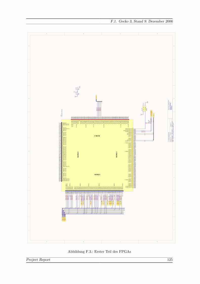
F.1. Gecko 3, Stand 9. Dezember 2006
11
22
33
44
55
66
77
88
DD
CC
BB
AA
D[0
..15]
INIT_B/WRXBUSY/RDYX
4.7K
R1_
FP1
3.3V
INIT
_B/W
RX
D[0
..15]
3
Ber
ne S
choo
l of A
pplie
d Sc
ienc
e
Sch
ool o
f Eng
inee
ring
and
Info
rmat
ion
Tech
nolo
gyQ
uellg
asse
21
CH
-250
1 B
iel
18
Gec
ko3:
FPG
A F
irst P
art
0.7
08.1
2.20
0615
:10:
25C
:\Doc
umen
ts a
nd S
ettin
gs\z
imm
c5\s
vn\fp
ga1.
Sch
Doc
Tite
l
Bla
ttgrö
sse:
Num
mer
:
Dat
um:
Dat
ei:
Rev
isio
n:
Bla
ttvo
nZe
it:
A3
39pF
C1_
FP1
39pF
C2_
FP1
2.5V
GN
D
Vre
f
INIT
_B/W
RX
BU
SY/R
DY
XB
USY
/RD
YX
OE
1
GN
D2
OU
T3
VC
C4
50M
Hz
Q1_
FP1
3.3V
GN
D
IO_L
01N
_6/V
RP_
6A
D2
IO_L
01P_
6/V
RN
_6A
D1
IO_L
02N
_6A
B4
IO_L
02P_
6A
B3
IO_L
03N
_6/V
RE
F_6
AC
2
IO_L
03P_
6A
C1
IO_L
05N
_6A
B2
IO_L
05P_
6A
B1
NC
AA
5
IO_L
06N
_6Y
7
IO_L
06P_
6Y
6
IO_L
07N
_6A
A4
IO_L
07P_
6A
A3
IO_L
08N
_6Y
5
IO_L
08P_
6Y
4
IO_L
09N
_6/V
RE
F_6
AA
2
IO_L
09P_
6A
A1
IO_L
10N
_6Y
2
IO_L
10P_
6Y
1
IO_L
14N
_6W
7
IO_L
14P_
6W
6
IO_L
16P_
6W
5
IO_L
16N
_6V
6
IO_L
17N
_6W
4
IO_L
17P_
6/V
REF
_6W
3
IO_L
19N
_6W
2
IO_L
19P_
6W
1
IO_L
20N
_6V
7
IO_L
20P_
6U
7
IO_L
21N
_6V
5
IO_L
21P_
6V
4
IO_L
22N
_6V
3
IO_L
22P_
6V
2
IO_L
23N
_6U
6
IO_L
23P_
6U
5
IO_L
24N
_6/V
RE
F_6
U4
IO_L
24P_
6U
3
IO_L
26N
_6U
2
IO_L
26P_
6U
1
IO_L
27N
_6T8
IO_L
27P_
6T7
IO_L
28N
_6T6
IO_L
28P_
6T5
IO_L
29N
_6T2
IO_L
29P_
6T1
IO_L
31N
_6R
8
IO_L
31P_
6R
7
IO_L
32N
_6R
6
IO_L
32P_
6R
5
IO_L
33N
_6T4
IO_L
33P_
6R
3
IO_L
34N
_6/V
RE
F_6
R2
IO_L
34P_
6R
1
IO_L
35N
_6P8
IO_L
35P_
6P7
IO_L
38N
_6P6
IO_L
38P_
6P5
IO_L
39N
_6P4
IO_L
39P_
6P3
IO_L
40N
_6P2
IO_L
40P_
6/V
REF
_6P1
IO_L01N_4/VRP_4 AB22
IO_L01P_4/VRN_4 AC22
IO/VREF_4 AD25
IO_L04N_4 AE24
IO_L04P_4 AF24
IO AD23
IO_L05N_4 AE23
IO_L05P_4 AF23
IO_L06N_4/VREF_4 AD22
IO_L06P_4 AE22
IO AF22
IO_L07N_4 AB21
IO_L07P_4 AC21
IO_L08N_4 AD21
IO_L08P_4 AE21
IO AF21
IO AA20
IO_L09N_4 AB20
IO_L09P_4 AC20
IO_L10N_4 AE20
IO_L10P_4 AF20
IO_L11N_4 Y19
IO_L11P_4 AA19
IO_L12N_4 AB19
IO_L12P_4 AC19
IO AD19
IO_L15N_4 AE19
IO_L15P_4 AF19
IO_L16N_4 Y18
IO_L16P_4 AA18
IO_L17N_4 AB18
IO_L17P_4 AC18
IO_L18N_4 AD18
IO_L18P_4 AE18
IO/VREF_4 Y17
IO_L19P_4 AA17
IO_L19N_4 AC17
IO_L22P_4 AB17
IO_L22N_4/VREF_4 AD17
IO_L23N_4 AE17
IO_L23P_4 AF17
IO W16
IO_L24N_4 Y16
IO_L24P_4 AA16
IO_L25N_4 AB16
IO_L25P_4 AC16
IO_L26N_4 AE16
IO_L26P_4/VREF_4 AF16
IO W15
IO_L27N_4/DIN/D0 Y15
IO_L27P_4/D1 W14
IO_L28N_4 AA15
IO_L28P_4 AB15
IO AD15
IO_L29N_4 AE15
IO_L29P_4 AF15
IO_L30N_4/D2 Y14
IO_L30P_4/D3 AA14
IO/VREF_4 AB14
IO_L31N_4/INIT_B AC14
IO_L31P_4/DOUT/BUSY AD14
IO_L32N_4/GCLK1 AE14
IO_L32P_4/GCLK0 AF14
IO_L
01N
_2/V
RP_
2C
25
IO_L
01P_
2/V
RN
_2C
26
IO_L
02N
_2E2
3
IO_L
02P_
2E2
4
IO_L
03P_
2D
26
IO_L
03N
_2/V
RE
F_2
D25
IO_L
05N
_2E2
5
IO_L
05P_
2E2
6
NC
F22
IO_L
06N
_2G
20
IO_L
06P_
2G
21
IO_L
07N
_2F2
3
IO_L
07P_
2F2
4
IO_L
08N
_2G
22
IO_L
08P_
2G
23
IO_L
09N
_2/V
RE
F_2
F25
IO_L
09P_
2F2
6
IO_L
10N
_2G
25
IO_L
10P_
2G
26
IO_L
14N
_2H
20
IO_L
14P_
2H
21
IO_L
16N
_2H
22
IO_L
16P_
2J2
1
IO_L
17P_
2/V
REF
_2H
24
IO_L
17N
_2H
23
IO_L
19N
_2H
25
IO_L
19P_
2H
26
IO_L
20N
_2J2
0
IO_L
20P_
2K
20
IO_L
21N
_2J2
2
IO_L
21P_
2J2
3
IO_L
22N
_2J2
4
IO_L
22P_
2J2
5
IO_L
23P_
2K
22
IO_L
23N
_2/V
RE
F_2
K21
IO_L
24N
_2K
23
IO_L
24P_
2K
24
IO_L
26N
_2K
25
IO_L
26P_
2K
26
IO_L
27N
_2L1
9
IO_L
27P_
2L2
0
IO_L
28N
_2L2
1
IO_L
28P_
2L2
2
IO_L
29N
_2L2
5
IO_L
29P_
2L2
6
IO_L
31N
_2M
19
IO_L
31P_
2M
20
IO_L
32N
_2M
21
IO_L
32P_
2M
22
IO_L
33P_
2M
24
IO_L
33N
_2L2
3
IO_L
34P_
2M
26
IO_L
34N
_2/V
RE
F_2
M25
IO_L
35N
_2N
19
IO_L
35P_
2N
20
IO_L
38N
_2N
21
IO_L
38P_
2N
22
IO_L
39N
_2N
23
IO_L
39P_
2N
24
IO_L
40N
_2N
25
IO_L
40P_
2/V
REF
_2N
26
IO_L32P_0/GCLK6A13
IO_L32N_0/GCLK7B13
IO_L31P_0/VREF_0C13
IO_L31N_0D13
IOE13
IO_L30P_0F13
IO_L30N_0G13
IO_L29P_0A12
IO_L29N_0B12
IOC12
IO_L28P_0E12
IO_L28N_0F12
IO_L27P_0H13
IO_L27N_0G12
IOH12
IO_L26P_0/VREF_0A11
IO_L26N_0B11
IO_L25P_0D11
IO_L25N_0E11
IO_L24P_0F11
IO_L24N_0G11
IOH11
IO_L23P_0A10
IO_L23N_0B10
IO_L22P_0C10
IO_L22N_0D10
IO_L19P_0E10
IO_L19N_0F10
IO/VREF_0G10
IO_L18P_0B9
IO_L18N_0C9
IO_L17P_0D9
IO_L17N_0E9
IO_L16P_0F9
IO_L16N_0G9
IO_L15P_0A8
IO_L15N_0B8
IOC8
IO_L12P_0D8
IO_L12N_0E8
IO_L11P_0F8
IO_L11N_0G8
IO_L10P_0A7
IO_L10N_0B7
IO_L09P_0D7
IO_L09N_0E7
IO/VREF_0F7
IOA6
IO_L08P_0B6
IO_L08N_0C6
IO_L07P_0D6
IO_L07N_0E6
IOA5
IO_L06P_0B5
IO_L06N_0C5
IO_L05P_0/VREF_0A4
IO_L05N_0B4
IOC4
IOA3
IO_L01P_0/VRN_0D5
IO_L01N_0/VRP_0E5
IO/VREF_0B3
BANK 6
BA
NK
0
BA
NK
4
BANK 2
XC
3S15
00-5
FG67
6CU
1A
Dra
m_D
1_[0
..15]
Dra
m_A
1_[0
..13]
Dra
m_U
DM
1
Dra
m_C
S1
Dra
m_C
KE1
Dra
m_C
K1
Dra
m_C
K1
Dra
m_U
DQ
S1
Dra
m_D
0_[0
..15]
Dra
m_A
0_[0
..13]
Dra
m_L
DM
0
Dra
m_U
DM
0
Dra
m_C
KE0
Dra
m_C
K0
Dra
m_C
K0
Dra
m_B
A0_
1
Dra
m_L
DQ
S0
Dra
m_U
DQ
S0
Dra
m_C
KE
0
Dra
m_U
DM
0
Dra
m_U
DQ
S0
Dra
m_C
K0
Dra
m_C
K0 V
ref
Vre
f
Vre
f
Vre
f
Vre
f
Vre
f
Dra
m_D
0_8
Dra
m_A
0_12
Dra
m_D
0_9
Dra
m_D
0_10
Dra
m_D
0_11
Dra
m_D
0_12
Dra
m_D
0_13
Dra
m_D
0_14
Dra
m_D
0_15
Dra
m_D
0_[0
..15]
Dra
m_C
S1
Dra
m_A
1_4
Dra
m_A
1_3
Dra
m_A
1_10
Dra
m_A
1_2
Dra
m_A
1_1
Dra
m_A
1_0
Dra
m_B
A0_
1
Dra
m_A
0_[0
..15]
Dra
m_D
1_[0
..15]
Dra
m_A
1_[0
..15]
Dra
m_D
0_0
Dra
m_D
0_1
Dra
m_D
0_2
Dra
m_D
0_3
Dra
m_D
0_4
Dra
m_D
0_5
Dra
m_D
0_6
Dra
m_D
0_13
Dra
m_L
DQ
S0
Dra
m_A
0_13
Dra
m_L
DM
0
Dra
m_A
1_5
Dra
m_A
1_6
Dra
m_A
1_7
Dra
m_A
1_8
Dra
m_A
1_9
Dra
m_A
1_11
Dra
m_A
1_12
Dra
m_C
KE1
Dra
m_C
K1
Dra
m_C
K1
Dra
m_U
DM
1D
ram
_UD
QS1
Flas
h_A
[0..2
3]Fl
ash_
A0
Flas
h_A
1Fl
ash_
A2
Flas
h_A
3Fl
ash_
A4
D6D7
D4D5
Abbildung F.3.: Erster Teil des FPGAs
Project Report 125

F. Schemas
11
22
33
44
55
66
77
88
DD
CC
BB
AA
RDWR_B/WRUCS_B/RDYU
4
Ber
ne S
choo
l of A
pplie
d Sc
ienc
e
Sch
ool o
f Eng
inee
ring
and
Info
rmat
ion
Tech
nolo
gyQ
uellg
asse
21
CH
-250
1 B
iel
18
Gec
ko3:
FPG
A S
econ
d P
art
0.7
08.1
2.20
0615
:10:
43C
:\Doc
umen
ts a
nd S
ettin
gs\z
imm
c5\s
vn\fp
ga2.
SC
HD
OC
Tite
l
Bla
ttgrö
sse:
Num
mer
:
Dat
um:
Dat
ei:
Rev
isio
n:
Bla
ttvo
nZe
it:
A3
39pF
C1_
FP2
39pF
C2_
FP2
2.5V
GN
D
Vre
f
D[0
..15]
D[0
..15]
CS_
B/R
DY
UR
DW
R_B
/WR
UC
S_B
/RD
YU
RD
WR
_B/W
RU
EXTCLK0EXTCLK1
IO_L
01P_
7/V
RN
_7F6
IO_L
01N
_7/V
RP_
7F5
IO_L
02P_
7E4
IO_L
02N
_7E3
IO_L
03P_
7D
2
IO_L
03N
_7/V
RE
F_7
D1
IO_L
05P_
7G
7
IO_L
05N
_7G
6
IO_L
06P_
7E2
IO_L
06N
_7E1
IO_L
07P_
7F4
IO_L
07N
_7F3
IO_L
08P_
7G
5
IO_L
08N
_7G
4
IO_L
09P_
7F2
IO_L
09N
_7F1
IO_L
10P_
7/V
REF
_7H
7
IO_L
10N
_7H
6
IO_L
14P_
7G
2
IO_L
14N
_7G
1
IO_L
16P_
7/V
REF
_7H
5
IO_L
16N
_7J6
IO_L
17P_
7H
4
IO_L
17N
_7H
3
IO_L
19P_
7H
2
IO_L
19N
_7/V
RE
F_7
H1
IO_L
20P_
7J7
IO_L
20N
_7K
7
IO_L
21P_
7J5
IO_L
21N
_7J4
IO_L
22P_
7J3
IO_L
22N
_7J2
IO_L
23P_
7K
6
IO_L
23N
_7K
5
IO_L
24P_
7K
4
IO_L
24N
_7K
3
IO_L
26P_
7K
2
IO_L
26N
_7K
1
IO_L
27P_
7/V
REF
_7L8
IO_L
27N
_7L7
IO_L
28P_
7L6
IO_L
28N
_7L5
IO_L
29P_
7L2
IO_L
29N
_7L1
IO_L
31P_
7M
8
IO_L
31N
_7M
7
IO_L
32N
_7M
6
IO_L
32P_
7M
5
IO_L
33P_
7L4
IO_L
33N
_7M
3
IO_L
34P_
7M
2
IO_L
34N
_7M
1
IO_L
35P_
7N
8
IO_L
35N
_7N
7
IO_L
38P_
7N
6
IO_L
38N
_7N
5
IO_L
39P_
7N
4
IO_L
39N
_7N
3
IO_L
40P_
7N
2
IO_L
40N
_7/V
RE
F_7
N1
IO AF4
IO_L01P_5/CS_B AB5
IO_L01N_5/RDWR_B AC5
IO_L04P_5 AD4
IO_L04N_5 AE4
IO/VREF_5 AF5
IO_L05P_5 AA6
IO_L05N_5 AB6
IO_L06P_5 AD5
IO_L06N_5 AE5
IO_L07P_5 AC6
IO_L07N_5 AD6
IO_L08P_5 AE6
IO_L08N_5 AF6
IO AA7
IO_L09P_5 AB7
IO_L09N_5 AC7
IO_L10P_5/VRN_5 AE7
IO_L10N_5/VRP_5 AF7
IO Y8
IO_L11P_5 AA8
IO_L11N_5/VREF_5 AB8
IO_L12P_5 AC8
IO_L12N_5 AD8
IO_L15P_5 AE8
IO_L15N_5 AF8
IO_L16P_5 Y9
IO_L16N_5 AA9
IO AB9
IO AC9
IO_L18P_5 AD9
IO_L18N_5 AE9
IO_L19P_5/VREF_5 Y10
IO_L19N_5 AA10
IO_L22P_5 AB10
IO_L22N_5 AC10
IO AD10
IO_L23P_5 AE10
IO_L23N_5 AF10
IO_L24P_5 W11
IO_L24N_5 Y11
IO_L25P_5 AA11
IO_L25N_5 AB11
IO AC11
IO_L26P_5 AE11
IO_L26N_5 AF11
IO_L27P_5 W12
IO_L27N_5/VREF_5 Y12
IO_L28P_5/D7 AA12
IO_L28N_5/D6 AB12
IO AD12
IO_L29P_5/VREF_5 AE12
IO_L29N_5 AF12
IO_L30P_5 W13
IO_L30N_5 Y13
IO AA13
IO_L31P_5/D5 AB13
IO_L31N_5/D4 AC13
IO_L32P_5/GCLK2 AD13
IO_L32N_5/GCLK3 AE13
IO/VREF_5 AF13
IO_L
40N
_3/V
RE
F_3
P26
IO_L
40P_
3P2
5
IO_L
39N
_3P2
4
IO_L
39P_
3P2
3
IO_L
38N
_3P2
2
IO_L
38P_
3P2
1
IO_L
35N
_3P2
0
IO_L
35P_
3P1
9
IO_L
34N
_3R
26
IO_L
34P_
3/V
REF
_3R
25
IO_L
33N
_3R
24
IO_L
33P_
3T2
3
IO_L
32N
_3R
22
IO_L
32P_
3R
21
IO_L
31N
_3R
20
IO_L
31P_
3R
19
IO_L
29N
_3T2
6
IO_L
29P_
3T2
5
IO_L
28N
_3T2
2
IO_L
28P_
3T2
1
IO_L
27N
_3T2
0
IO_L
27P_
3T1
9
IO_L
26N
_3U
26
IO_L
26P_
3U
25
IO_L
24N
_3U
24
IO_L
24P_
3U
23
IO_L
23N
_3U
22
IO_L
23P_
3/V
REF
_3U
21
IO_L
22N
_3V
25
IO_L
22P_
3V
24
IO_L
21N
_3V
23
IO_L
21P_
3V
22
IO_L
20N
_3U
20
IO_L
20P_
3V
20
IO_L
19N
_3W
26
IO_L
19P_
3W
25
IO_L
17N
_3W
24
IO_L
17P_
3/V
REF
_3W
23
IO_L
16N
_3V
21
IO_L
16P_
3W
22
IO_L
14N
_3Y
26
IO_L
14P_
3Y
25
IO_L
10N
_3W
21
IO_L
10P_
3W
20
IO_L
09N
_3A
A26
IO_L
09P_
3/V
REF
_3A
A25
IO_L
08N
_3Y
23
IO_L
08P_
3Y
22
IO_L
07N
_3A
A24
IO_L
07P_
3A
A23
IO_L
06N
_3A
B26
IO_L
06P_
3A
B25
IO_L
05N
_3Y
21
IO_L
05P_
3Y
20
IO_L
03N
_3A
C26
IO_L
03P_
3A
C25
IO_L
02N
_3/V
RE
F_3
AB
24
IO_L
02P_
3A
B23
IO_L
01N
_3/V
RP_
3A
A22
IO_L
01P_
3/V
RN
_3A
A21
IOA14
IO_L32N_1/GCLK5B14
IO_L32P_1/GCLK4C14
IO_L31N_1/VREF_1D14
IO_L31P_1E14
IOF14
IO_L30N_1G14
IO_L30P_1H14
IO_L29N_1A15
IO_L29P_1B15
IO/VREF_1C15
IO_L28N_1E15
IO_L28P_1F15
IO_L27N_1G15
IO_L27P_1H15
IO_L26N_1A16
IO_L26P_1B16
IOD16
IO_L25N_1E16
IO_L25P_1F16
IO_L24N_1G16
IO_L24P_1H16
IO_L23N_1A17
IO_L23P_1B17
IO/VREF_1C17
IO_L22N_1D17
IO_L22P_1E17
IO_L19N_1F17
IO_L19P_1G17
IO_L18N_1B18
IO_L18P_1C18
IO/VREF_1D18
IOE18
IO_L16N_1F18
IO_L16P_1G18
IO_L15N_1A19
IO_L15P_1B19
IO_L12N_1C19
IO_L12P_1D19
IO_L11N_1E19
IO_L11P_1F19
IOG19
IO_L10N_1/VREF_1A20
IO_L10P_1B20
IO_L09N_1D20
IO_L09P_1E20
IOF20
IO_L08N_1A21
IO_L08P_1B21
IO_L07N_1C21
IO_L07P_1D21
IO_L06N_1/VREF_1B22
IO_L06P_1C22
IO_L05N_1E21
IO_L05P_1F21
IOA22
IO_L04N_1B23
IO_L04P_1C23
IO_L01N_1/VRP_1D22
IO_L01P_1/VRN_1E22
IOA23
BANK 7
BA
NK
1
BA
NK
5
BANK 3
XC
3S15
00-5
FG67
6CU
1B
Dra
m_D
1_[0
..15]
Dra
m_A
1_[0
..13]
Dra
m_L
DM
1
Dra
m_W
E1D
ram
_CA
S1
Dra
m_R
AS1
Dra
m_B
A1_
1
Dra
m_B
A1_
0
Dra
m_C
S0
Dra
m_W
E0D
ram
_CA
S0
Dra
m_R
AS0
Dra
m_B
A0_
0
Dra
m_L
DQ
S1
2.5V
I/O
Ban
k ne
eded
Vre
f
Vre
f
Vre
f
Vre
f
Vre
f
Vre
f
Dra
m_A
0_5
Dra
m_A
0_6
Dra
m_A
0_7
Dra
m_A
0_8
Dra
m_A
0_9
Dra
m_A
0_11
Dra
m_A
0_[0
..13]
Dra
m_D
1_0
Dra
m_D
1_1
Dra
m_D
1_2
Dra
m_D
1_3
Dra
m_D
1_4
Dra
m_D
1_5
Dra
m_D
1_6
Dra
m_D
1_13
Dra
m_L
DQ
S1
Dra
m_A
1_13
Dra
m_C
AS1
Dra
m_B
A1_
1D
ram
_RA
S1
Dra
m_W
E1
Dra
m_L
DM
1
Dra
m_D
0_[0
..15]D
ram
_D0_
[0..1
5]D
ram
_A0_
[0..1
5]D
ram
_D1_
[0..1
5]D
ram
_A1_
[0..1
5]
Dra
m_W
E0
Dra
m_B
A0_
0
Dra
m_C
AS0
Dra
m_R
AS0
Dra
m_C
S0
Dra
m_B
A1_
0D
ram
_A0_
0
Dra
m_A
0_1
Dra
m_A
0_2
Dra
m_A
0_10
Dra
m_A
0_3
Dra
m_A
0_4
Dra
m_D
1_8
Dra
m_D
1_9
Dra
m_D
1_10
Dra
m_D
1_11
Dra
m_D
1_12
Dra
m_D
1_13
Dra
m_D
1_14
Dra
m_D
1_15
D0D1
D2D3
Abbildung F.4.: Zweiter Teil des FPGAs
126 Christoph Zimmermann
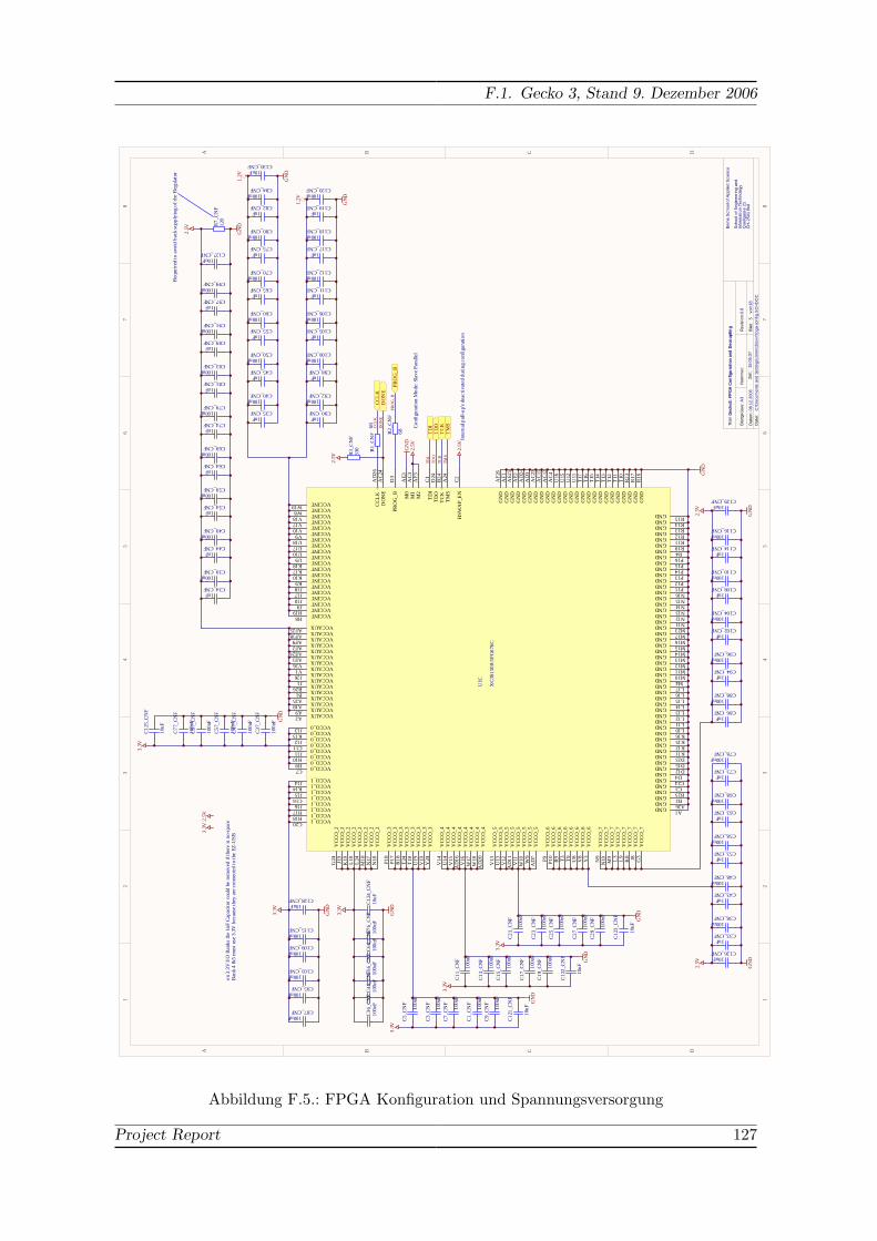
F.1. Gecko 3, Stand 9. Dezember 2006
11
22
33
44
55
66
77
88
DD
CC
BB
AA
3.3V
1.2V
2.5V
CCL
KD
ON
E
PRO
G_B
Ban
k 4
&5
mus
t use
3.3
V b
ecau
se th
ey a
re c
onne
cted
to th
e EZ
-USB
68R
1_C
NF
330
R3_
CN
F
68R2_
CN
F
2.5V
120
R7_
CN
F
Req
urir
ed to
avo
id b
ack
supp
lyin
g of
the
Reg
ulat
or
2.5V
2.5V
GN
D
Con
figu
ratio
n M
ode:
Sla
ve P
aral
lel
5
Ber
ne S
choo
l of A
pplie
d S
cien
ce
Sch
ool o
f Eng
inee
ring
and
Info
rmat
ion
Tech
nolo
gyQ
uellg
asse
21
CH
-250
1 Bi
el18
Gec
ko3:
FP
GA
Con
figu
rati
on a
nd D
eco
uplin
g
0.8
08.1
2.20
0615
:06:
37C
:\Doc
umen
ts a
nd S
ettin
gs\z
imm
c5\s
vn\fp
ga-c
onfig
.SC
HD
OC
Tite
l
Bla
ttgrö
sse:
Num
mer
:
Dat
um:
Dat
ei:
Rev
isio
n:
Bla
ttvo
nZe
it:
A3
3.3V
100nFC40_CNF
1nFC35_CNF
GN
D
100nFC50_CNF
1nFC45_CNF
100nFC60_CNF
1nFC55_CNF
100nFC70_CNF
1nFC65_CNF
100nFC80_CNF
1nFC75_CNF
100nFC84_CNF
1nFC82_CNF
100nFC92_CNF
1nFC90_CNF
100nFC100_CNF
1nFC98_CNF
100nFC106_CNF
1nFC105_CNF
100nFC112_CNF
1nFC111_CNF
100nFC118_CNF
1nFC117_CNF
100nFC120_CNF
1nFC119_CNF
100nFC39_CNF
1nFC34_CNF
100nFC49_CNF
1nFC44_CNF
100nFC59_CNF
1nFC54_CNF
100nFC69_CNF
1nFC64_CNF
100nFC79_CNF
1nFC74_CNF
100nFC83_CNF
1nFC81_CNF
100nFC91_CNF
1nFC89_CNF
100nFC99_CNF
1nFC97_CNF
GN
D
2.5V
100nFC38_CNF
1nFC33_CNF
100nFC48_CNF
1nFC43_CNF
100nFC58_CNF
1nFC53_CNF
100nFC68_CNF
1nFC63_CNF
100nFC78_CNF
1nFC73_CNF
100nFC88_CNF
1nFC86_CNF
100nFC96_CNF
1nFC94_CNF
100nFC104_CNF
1nFC102_CNF
100nFC110_CNF
1nFC108_CNF
100nFC116_CNF
1nFC114_CNF
GN
D
100n
F
C37
_CN
F10
0nF
C47
_CN
F10
0nF
C57
_CN
F10
0nF
C67
_CN
F10
0nF
C77
_CN
F
GN
D
100nFC87_CNF
100nFC95_CNF
100nFC103_CNF
100nFC109_CNF
100nFC115_CNF
GN
D
100n
FC
36_C
NF
100n
FC
46_C
NF 10
0nF
C56
_CN
F10
0nF
C66
_CN
F 100n
FC
76_C
NF G
ND
100n
F
C21
_CN
F
100n
F
C23
_CN
F
100n
F
C25
_CN
F
100n
F
C27
_CN
F
100n
F
C29
_CN
F GN
D
100n
F
C11
_CN
F
100n
F
C13
_CN
F
100n
F
C15
_CN
F
100n
F
C17
_CN
F
100n
F
C19
_CN
F GN
D
100n
F
C1_
CN
F
100n
F
C3_
CN
F
100n
F
C5_
CN
F
100n
F
C7_
CN
F
100n
F
C9_
CN
F GN
D
3.3V
on 3
.3V
I/O
Ban
ks th
e 1n
F C
apac
itor
coul
d be
rem
oved
if th
ere
is n
o sp
ace
DO
NE
PRO
G_B
CC
LK
Inte
rnal
pul
l-up'
s de
activ
ated
dur
ing
conf
igur
atio
n
TDI
TDO
TCK
TMS
TC
K
TD
I
TM
S
TD
O
10uF
C12
1_C
NF
10uF
C12
2_C
NF
10uF
C12
3_C
NF
10uFC130_CNF
10uFC127_CNF
10uFC129_CNF
10uFC128_CNF
10uF
C12
4_C
NF
10uF
C12
5_C
NF
2.5V
2.5V
3.3V
3.3V
3.3V
3.3V
TM
SA
24
DO
NE
AC
24
M1
AC
3
CC
LK
AD
26
M0
AE3
M2
AF3
TC
KB
24
HSW
AP_
EN
C2
TD
IC
1
PRO
G_B
D3
TD
OD
24GND A1
GND A26
GND B2
GND B25
GND C3
GND C24
GND D4
GND D12
GND D15
GND D23
GND K11
GND K12
GND K15
GND K16
GND L10
GND L11
GND L12
GND L13
GND L14
GND L15
GND L16
GND L17
GND M4
GND M10
GND M11
GND M12
GND M13
GND M14
GND M15
GND M16
GND M17
GND M23
GND N11
GND N12
GND N13
GND N14
GND N15
GND N16
GND P11
GND P12
GND P13
GND P14
GND P15
GND P16
GND R4
GND R10
GND R11
GND R12
GND R13
GND R14
GND R15
GN
DR
16G
ND
R17
GN
DR
23G
ND
T10
GN
DT
11G
ND
T12
GN
DT
13G
ND
T14
GN
DT
15G
ND
T16
GN
DT
17G
ND
U11
GN
DU
12G
ND
U15
GN
DU
16G
ND
AC
4G
ND
AC
12G
ND
AC
15G
ND
AC
23G
ND
AD
3G
ND
AD
24G
ND
AE2
GN
DA
E25
GN
DA
F1G
ND
AF2
6
VCCAUXA2
VCCAUXA9
VCCAUXA18
VCCAUXA25
VCCAUXB1
VCCAUXB26
VCCAUXJ1
VCCAUXJ26
VCCAUXV1
VCCAUXV26
VCCAUXAE1
VCCAUXAE26
VCCAUXAF2
VCCAUXAF9
VCCAUXAF18
VCCAUXAF25
VCCINTH8
VCCINTH19
VCCINTJ9
VCCINTJ10
VCCINTJ17
VCCINTJ18
VCCINTK9
VCCINTK10
VCCINTK17
VCCINTK18
VCCINTU9
VCCINTU10
VCCINTU17
VCCINTU18
VCCINTV9
VCCINTV10
VCCINTV17
VCCINTV18
VCCINTW8
VCCINTW19
VC
CO
_6Y
3V
CC
O_6
V8
VC
CO
_6U
8V
CC
O_6
T9
VC
CO
_6T
3V
CC
O_6
R9
VC
CO
_6P1
0V
CC
O_6
P9
VC
CO
_4A
D20
VC
CO
_4W
18V
CC
O_4
W17
VC
CO
_4V
16V
CC
O_4
AD
16V
CC
O_4
V15
VC
CO
_4U
14V
CC
O_4
V14
VC
CO
_2G
24
VC
CO
_2J1
9
VC
CO
_2K
19
VC
CO
_2L
18
VC
CO
_2L
24
VC
CO
_2M
18
VC
CO
_2N
17
VC
CO
_2N
18
VCCO_0J13 VCCO_0K13 VCCO_0J12 VCCO_0C11 VCCO_0J11 VCCO_0H10 VCCO_0H9 VCCO_0C7
VC
CO
_7G
3V
CC
O_7
J8V
CC
O_7
K8
VC
CO
_7L
9V
CC
O_7
L3
VC
CO
_7M
9V
CC
O_7
N10
VC
CO
_7N
9
VC
CO
_5A
D7
VC
CO
_5W
9V
CC
O_5
W10
VC
CO
_5V
11V
CC
O_5
AD
11V
CC
O_5
V12
VC
CO
_5U
13V
CC
O_5
V13
VC
CO
_3P1
8
VC
CO
_3P1
7
VC
CO
_3R
18
VC
CO
_3T
24
VC
CO
_3T
18
VC
CO
_3U
19
VC
CO
_3V
19
VC
CO
_3Y
24
VCCO_1J14 VCCO_1K14 VCCO_1J15 VCCO_1C16 VCCO_1J16 VCCO_1H17 VCCO_1H18 VCCO_1C20
XC
3S15
00-5
FG67
6C
U1C
GN
D
1.2V
GN
D
GN
D10uFC126_CNF
Abbildung F.5.: FPGA Konfiguration und Spannungsversorgung
Project Report 127
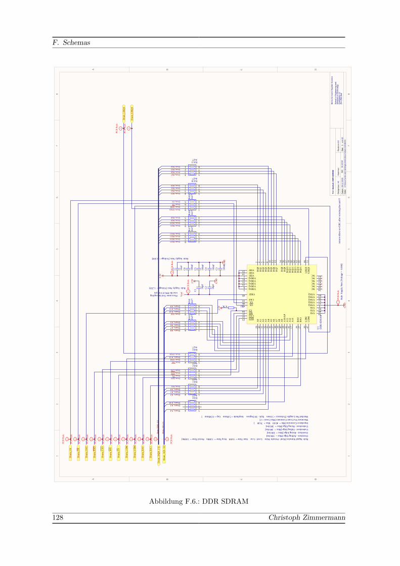
F. Schemas
11
22
33
44
55
66
77
88
DD
CC
BB
AA
Dra
m_D
Q[0
..15]
Dra
m_A
[0..1
3]
GN
D
2.5V
100n
F
C6
39pF
C1 39
pF
C2
2.5V
GN
D
Vre
f
VDD1
DQ
02
VDDQ3
DQ
14
VSSQ 6
DQ
25
VDDQ9
DQ
37
VSSQ 12
VDD18
NC 14
WE21 CAS22 RAS23
CS24
BA
026
BA
127
A10
/AP
28
A0
29
A1
30
A2
31
A3
32
VDD33
VSS 66
A4
35
A5
36
A6
37
A7
38
A8
39
A9
40
A11
41
A12
42
CKE44
NC 19
VSS 48
NC 43VDDQ55
DQ
48
NC 50
VSSQ 52
DQ
510
NC 53
VDDQ15
DQ
611
NC 25
VSSQ 58
DQ
713
VSS 34
A13
17
VSSQ 64
VDDQ61D
Q8
54
DQ
956
DQ
1057
DQ
1159
DQ
1260
DQ
1362
DQ
1463
DQ
1565
CK45
CK46
LD
M20
UD
M47
UD
QS
51L
DQ
S16
VREF49
DD
R-S
DR
AM
U1
GN
D
Place same Vref decoupling
100n
F
C5
100n
F
C4
100n
F
C3
1234 5
678
4x27RA1
iPC
B R
ule
Rule: Supply Nets [Voltage = 2.500]
iPC
B R
ule
Rule: Supply Nets [Voltage = 1.250]
iPC
B R
ule
Rul
e: S
uppl
y N
ets
[Vol
tage
= 0
.000
]
i
PCB
Rul
e
4.7K R1
2.5V
Dram_BA0
Dram_BA1
Dram_LDM
Dram_UDMDram_UDQS
Dram_LDQS
Dram_DQ0Dram_DQ1Dram_DQ2Dram_DQ3
Dram_DQ4Dram_DQ5Dram_DQ6Dram_DQ7
Dram_DQ8Dram_DQ9Dram_DQ10Dram_DQ11
Dram_DQ12Dram_DQ13Dram_DQ14Dram_DQ15
Dram_RASDram_CAS
Dram_WE
Dram_CS
Dram_CKDram_CK
Dram_CKE
i
PCB
Rul
e
Rule: Signal Stimulus [Kind - Periodic Pulse Level - Low Start Time = 0.000 Stop Time = 1.800n Period Time = 3.600n]Overshoot - Falling Edge [Max = 300.0m]Overshoot - Rising Edge [Max = 300.0m]Undershoot - Falling Edge [Max = 300.0m]Undershoot - Rising Edge [Max = 300.0m]Impedance Constraint [Min = 40.00 Max = 70.00 ]Maximum Via Count Constraint [Max Count = 2]Matched Net Lengths [Tolerance = 3.6mm Style - 90 Degrees Amplitude = 5.08mm Gap = 0.508mm ]
Dra
m_A
[0..1
3]
Dra
m_D
Q[0
..15]
Dra
m_L
DM
Dra
m_U
DM
6
Ber
ne S
choo
l of A
pplie
d S
cien
ce
Sch
ool o
f Eng
inee
ring
and
Info
rmat
ion
Tech
nolo
gyQ
uellg
asse
21
CH
-250
1 Bi
el18
Gec
ko3:
DD
R S
DR
AM
0.8
08.1
2.20
0615
:14:
54C
:\Doc
umen
ts a
nd S
ettin
gs\z
imm
c5\s
vn\d
ram
.SC
HD
OC
Tite
l
Bla
ttgrö
sse:
Num
mer
:
Dat
um:
Dat
ei:
Rev
isio
n:
Bla
ttvo
nZe
it:
A3
1234 5
678
4x27RA2
1234 5
678
4x27RA3
1234 5
678
4x27RA4
12345
678
4x27
RA
5
12345
678
4x27
RA
6
12345
678
4x27
RA
7
12345
678
4x27
RA
8
12345
678
4x27
RA
9
1234 5
678
4x27RA10
1234 5
678
4x27RA11
i
PCB
Rul
e
i
PCB
Rul
e
i
PCB
Rul
e
i
PCB
Rul
e
i
PCB
Rul
e
i
PCB
Rul
e
i
PCB
Rul
e
i
PCB
Rul
e
Dra
m_C
S
Dra
m_W
E
Dra
m_C
AS
Dra
m_R
AS
Dra
m_C
KE
Dra
m_C
K
Dra
m_C
K
Dra
m_B
A1
i
PCB
Rul
eD
ram
_BA
0i
PCB
Rul
e
Dra
m_L
DQ
S
Dra
m_U
DQ
S
i
PCB
Rul
e
i
PCB
Rul
e
i
PCB
Rul
e
rem
ove
thes
e no
-ER
C a
fter
wir
erin
g th
e ra
m!!
!
10uF
C7
near the FPGA Vref pin
Dram_A0Dram_A1Dram_A2
Dram_A3
Dram_A4
Dram_A5Dram_A6Dram_A7Dram_A8
Dram_A9
Dram_A10
Dram_A11Dram_A12
Dram_A13
Abbildung F.6.: DDR SDRAM
128 Christoph Zimmermann

F.1. Gecko 3, Stand 9. Dezember 2006
11
22
33
44
DD
CC
BB
AA
A19
5A
186
A17
7A
168
A15
10A
1411
A13
12A
1213
CE0 14
VCC37
Vpen15
RP16
A11
17A
1018
A9
19A
820
A7
22A
623
A5
24A
425
A3
26A
227
A1
28A
032
DQ
033
DQ
135
DQ
238
DQ
340
GND 42GND 21
VCCQ43
DQ
444
DQ
546
DQ
649
DQ
751
STS
53
OE54
WE55
A20
4
DQ
834
DQ
936
DQ
1039
DQ
1141
DQ
1245
DQ
1347
DQ
1450
DQ
1552
A21
3
A22
1
A23
30
GND 48
NC 56
CE1 2
CE2 29
VCC9
BYTE31JS
28F1
28J3
D-7
5U
2
Flas
h_D
Q[0
..15]
Flas
h_A
[0..2
3]
7
Ber
ne S
choo
l of A
pplie
d S
cien
ce
Sch
ool o
f Eng
inee
ring
and
Info
rmat
ion
Tech
nolo
gyQ
uellg
asse
21
CH
-250
1 Bi
el18
Gec
ko3:
NO
R F
lash
0.7
08.1
2.20
0614
:57:
43C
:\Doc
umen
ts a
nd S
ettin
gs\z
imm
c5\s
vn\fl
ash.
Sch
Doc
Tite
l
Bla
ttgrö
sse:
Num
mer
:
Dat
um:
Dat
ei:
Rev
isio
n:
Bla
ttvo
nZe
it:
A4
4.7K
R2
3.3V
GN
DG
ND
Dis
able
s Fla
sh d
urin
g FP
GA
con
figur
atio
n
3.3V
4.7KR3
GN
D
100nFC10
100nFC9
100nFC8
4.7KR4
Flas
h_A
0Fl
ash_
A1
Flas
h_A
2Fl
ash_
A3
Flas
h_A
4Fl
ash_
A5
Flas
h_A
6Fl
ash_
A7
Flas
h_A
8Fl
ash_
A9
Flas
h_A
10Fl
ash_
A11
Flas
h_A
12Fl
ash_
A13
Flas
h_A
14Fl
ash_
A15
Flas
h_A
16Fl
ash_
A17
Flas
h_A
18Fl
ash_
A19
Flas
h_A
20Fl
ash_
A21
Flas
h_A
22Fl
ash_
A23
Flas
h_C
E0
Flas
h_O
EFl
ash_
RP
Flas
h_W
EFl
ash_
BY
TE
Flas
h_D
Q0
Flas
h_D
Q1
Flas
h_D
Q2
Flas
h_D
Q3
Flas
h_D
Q4
Flas
h_D
Q5
Flas
h_D
Q6
Flas
h_D
Q7
Flas
h_D
Q8
Flas
h_D
Q9
Flas
h_D
Q10
Flas
h_D
Q11
Flas
h_D
Q12
Flas
h_D
Q13
Flas
h_D
Q14
Flas
h_D
Q15
Flas
h_D
Q[0
..15]
Flas
h_B
YTE
Flas
h_W
EFl
ash_
RP
Flas
h_O
E
Flas
h_C
E0
Flas
h_A
[0..2
3]
Abbildung F.7.: paralleles NOR Flash
Project Report 129

F. Schemas
11
22
33
44
DD
CC
BB
AA
D[0
..15]
VccB5 VccC5 VccE8 VccE7 VccG1 VccA5
GND A4GND C4GND D8GND D7GND H1GND B4
INT0
/PA
0G
8IN
T1/P
A1
G6
SLO
E/P
A2
F8W
U2/
PA3
F7FI
FOA
DR
0/PA
4F6
FIFO
AD
R1/
PA5
C8
PKTE
ND
/PA
6C
7Fl
agD
/SL
CS/
PA7
C6
PB0/
FD0
H3
PB1/
FD1
F4PB
2/FD
2H
4PB
3/FD
3G
4PB
4/FD
4H
5PB
5/FD
5G
5PB
6/FD
6F5
PB7/
FD7
H6
PD0/
FD8
A8
PD1/
FD9
A7
PD2/
FD10
B6
PD3/
FD11
A6
PD4/
FD12
B3
PD5/
FD13
A3
PD6/
FD14
C3
PD7/
FD15
A2
AVccD2 AVccD1 AGND F2AGND F1
Reserved H2
RE
SET
B8
Wak
eup
B7
Xta
lIn
C1
Xta
lOut
C2
IFC
LK
G2
CL
KO
UT
B2
D+
E2
D-
E1
SCL
F3
SDA
G3
SLR
D/R
DY
0A
1
SLW
R/R
DY
1B
1
Flag
A/C
TL0
H7
Flag
B/C
TL1
G7
Flag
C/C
TL2
H8
EZ-
USB
FX
2LP
CY
7C68
013A
-56B
AX
C
U1_
USB
D+ID D-
GN
D
Vbu
s
shieldshieldU
SB-M
INIB
JP1_
USB
avoi
ds th
at th
e cu
rren
t on
Vbu
s ca
n fl
ow in
rev
erse
dir
ectio
n
22pF
C2_
USB
22pF
C3_
USB
GN
DG
ND
CT
L3
GN
D2
IN1
OU
T5
STA
T4
LTC
4411
U2_
USB
GN
D
GN
D
Vbu
s
GN
D
3.3V
1M_2
50V
R1_
USB
100nF
C6_
USB
10nF
C5_
USB
3.3V
GN
D
100n
F
C7_
USB
1nF
C8_
USB
100n
F
C9_
USB
100n
F
C10
_USB
100n
F
C11
_USB
GN
D10
0nF
C12
_USB
300k
R2_
USB 10
0nF
C4_
USB
GN
D
3.3V
D0
D1
D2
D3
D4
D5
D6
D7
D8
D9
D10
D11
D12
D13
D14
D15
INIT
_B/W
RX
BU
SY/R
DY
X
CC
LKR
DW
R_B
/WR
UC
S_B
/RD
YU
DO
NE
DO
NE
RES
ET
SCLK
MO
SIM
ISO
SPI_
CS_
F
PRO
G_B
Vbu
s
D[0
..15]
8
Ber
ne S
choo
l of A
pplie
d S
cien
ce
Sch
ool o
f Eng
inee
ring
and
Info
rmat
ion
Tech
nolo
gyQ
uellg
asse
21
CH
-250
1 Bi
el18
Gec
ko3:
US
B a
nd
FPG
A B
oot S
yste
m
0.8
08.1
2.20
0615
:14:
23C
:\Doc
umen
ts a
nd S
ettin
gs\z
imm
c5\s
vn\u
sb.S
CH
DO
C
Tite
l
Bla
ttgrö
sse:
Num
mer
:
Dat
um:
Dat
ei:
Rev
isio
n:
Bla
ttvo
nZe
it:
A4
MLB-160808-S600Q
FB1_USB
DO
NE
INIT
_B/W
RX
PRO
G_B
RD
WR
_B/W
RU
BU
SY/R
DY
X
RE
SET
CS_
B/R
DY
U
CC
LK
MIS
OSP
I_C
S_F
MO
SISC
LK
RES
ET
PRO
G_B
INIT
_B/W
RX
BU
SY/R
DY
XC
CLK
RD
WR
_B/W
RU
CS_
B/R
DY
U
(exa
mpl
e fr
om th
e C
olib
ri b
oard
to th
e G
ecko
)
SDA
SCL
24M
Hz
Q1_
USB
2.2u
F
C13
_USB
4.7n
F_25
0VC
1_U
SB
SDA
SCL
2.2K
R3_USB 2.2K
R4_USB
3.3V
Rep
rogr
amm
But
ton
S1_U
SB
Vbu
s_sw
Abbildung F.8.: USB 2.0 und FPGA Boot System
130 Christoph Zimmermann
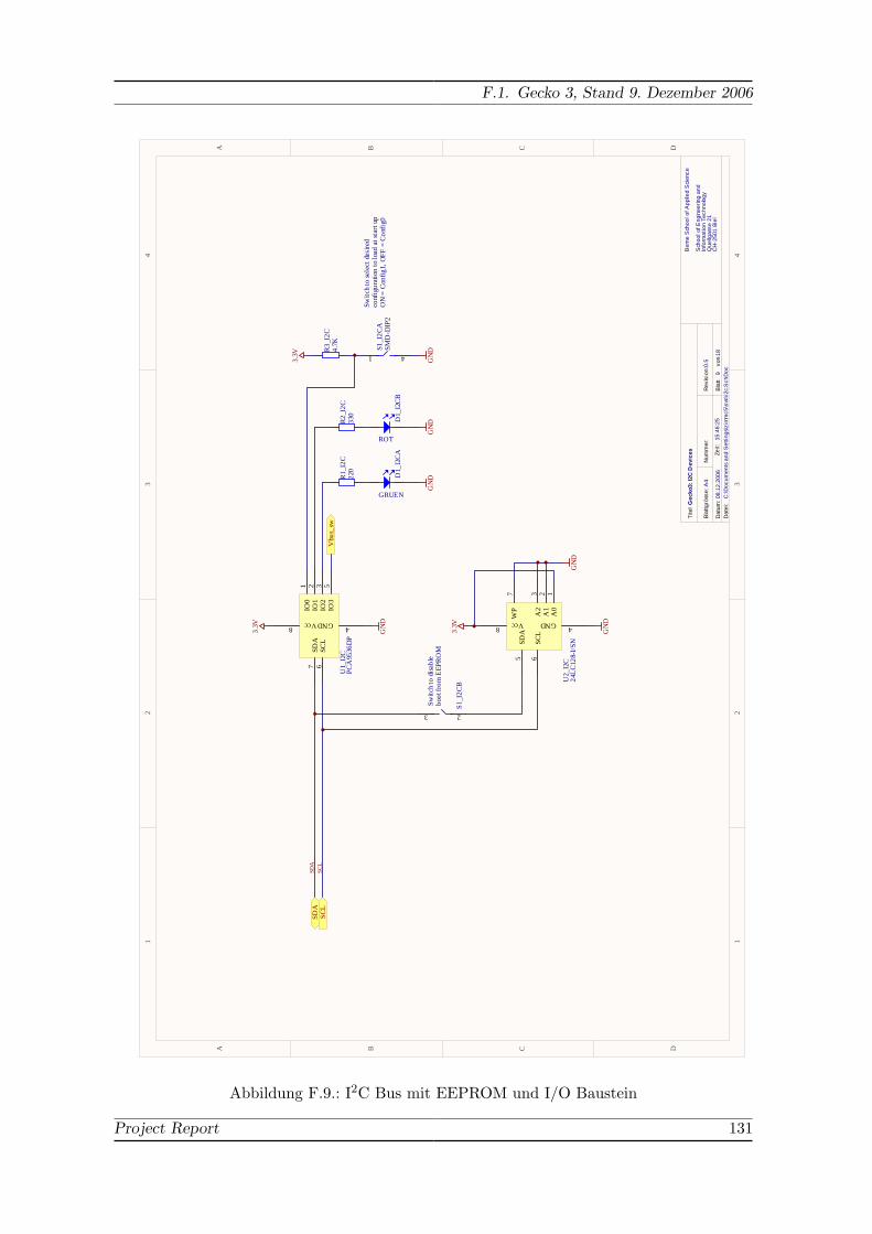
F.1. Gecko 3, Stand 9. Dezember 2006
11
22
33
44
DD
CC
BB
AA
9
Ber
ne S
choo
l of A
pplie
d S
cien
ce
Sch
ool o
f Eng
inee
ring
and
Info
rmat
ion
Tech
nolo
gyQ
uellg
asse
21
CH
-250
1 Bi
el18
Gec
ko3:
I2C
Dev
ices
0.5
08.1
2.20
0615
:46:
25C
:\Doc
umen
ts a
nd S
ettin
gs\z
imm
c5\s
vn\i2
c.S
chD
oc
Tite
l
Bla
ttgrö
sse:
Num
mer
:
Dat
um:
Dat
ei:
Rev
isio
n:
Bla
ttvo
nZe
it:
A4
GN
D
3.3V
GN
D
23
S1_I
2CB
Switc
h to
dis
able
boot
from
EEP
RO
M
SDA
SCL
SDA
SCL
ROT
D1_
I2C
B
330
R2_
I2C
1 4
SMD
-DIP
2S1
_I2C
A
220
R1_
I2C
GRUEN
D1_
I2C
A
GN
D
Switc
h to
sel
ect d
esire
dco
nfig
urat
ion
to lo
ad a
t sta
rt u
pO
N =
Con
fig1,
OFF
= C
onfi
g0
IO2
3
IO3
5
GND 4Vcc8
SDA
7
SCL
6
IO0
1
IO1
2
PCA
9536
DP
U1_
I2C
GN
D
3.3V
4.7K
R3_
I2C
GN
D
3.3V
GN
D
Vbu
s_sw
GND 4Vcc8
SDA
5
SCL
6
WP
7
A2
3
A1
2
A0
1
24L
C12
8-I/
SNU
2_I2
C
Abbildung F.9.: I2C Bus mit EEPROM und I/O Baustein
Project Report 131
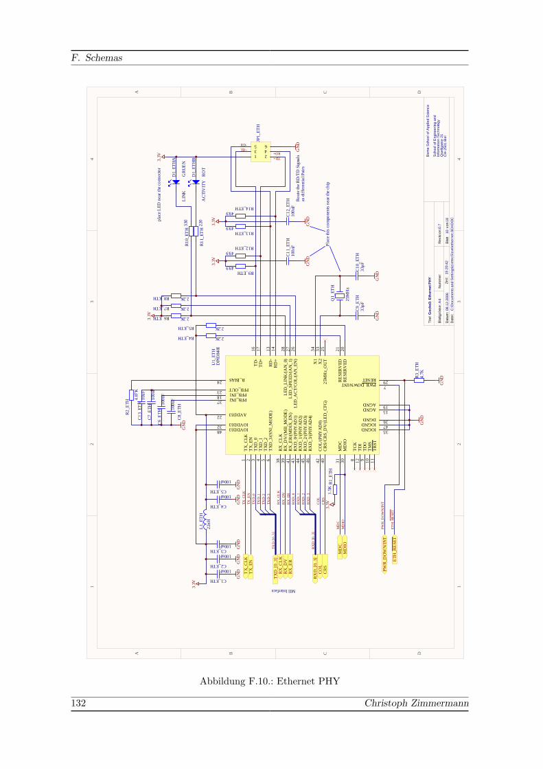
F. Schemas
11
22
33
44
DD
CC
BB
AA
PWR
_DO
WN
/IN
T
ETH
_RE
SET
22nH
L1_
ETH
1.5K
R1_
ETH
100nFC3_ETH
GN
D
GN
D
33pF
C9_
ETH
33pF
C10
_ET
H
GN
DG
ND
49.9R12_ETH
49.9R9_ETH
100n
FC
11_E
TH
3.3V
3.3V
GN
D
GN
D
49.9R14_ETH
49.9R13_ETH
100n
FC
12_E
TH
3.3V
3.3V
2.2KR4_ETH
2.2KR5_ETH
2.2KR6_ETH
2.2KR7_ETH
2.2KR8_ETH
330
R10
_ET
H
220
R11
_ET
H
LIN
K
AC
TIV
ITY
4.87
K
R2_
ETH
100n
FC
8_E
TH
100n
FC
6_E
TH10
0nF
C7_
ETH
GN
D
100nF
C4_ETH
100nF
C5_ETH
GN
DG
ND
100nF
C2_ETH100nF
C1_ETH
GN
DG
ND
GN
D
3.3V
3.3VTX
_CLK
TX_E
NTX
D_0
TXD
_1TX
D_2
TXD
_3
RX
D_0
RX
D_1
RX
D_2
RX
D_3
RX
_CL
KR
X_D
VR
X_E
R
CO
LC
RS
Plac
e th
is c
ompo
nent
s ne
ar th
e ch
ip
PWR
_DO
WN
/INT
ETH
_RE
SET
10
Ber
ne S
choo
l of A
pplie
d S
cien
ce
Sch
ool o
f Eng
inee
ring
and
Info
rmat
ion
Tech
nolo
gyQ
uellg
asse
21
CH
-250
1 Bi
el18
Gec
ko3:
Eth
erne
t PH
Y
0.7
08.1
2.20
0615
:20:
42C
:\Doc
umen
ts a
nd S
ettin
gs\z
imm
c5\s
vn\e
ther
net.S
CH
DO
C
Tite
l
Bla
ttgrö
sse:
Num
mer
:
Dat
um:
Dat
ei:
Rev
isio
n:
Bla
ttvo
nZe
it:
A4
TD-
TD+
RD-
RD+
Rou
te th
e R
D/T
D S
igna
lsas
dif
fere
ntia
l Pai
rs
1 23 45 6
JP1_
ETH
GR
UE
N
D1_
ETH
A
RO
T
D1_
ETH
B
MD
C31
MD
IO30
TX
_CLK
1
TX
_EN
2
TX
D_0
3
TX
D_1
4
TX
D_2
5
TX
D_3
/(SN
I_M
OD
E)
6
RX
_CL
K38
RX
_DV
/(M
II_M
OD
E)
39
RX
_ER
/(MD
IX_E
N)
41
RX
D_0
/(PH
YA
D1)
43
RX
D_1
/(PH
YA
D2)
44
RX
D_2
/(PH
YA
D3)
45
RX
D_3
/(PH
YA
D4)
46
CR
S/C
RS_
DV
/(LE
D_C
FG)
40C
OL/
(PH
YA
D0)
42X
134
X2
33
25M
Hz_
OU
T25
LED
_LIN
K/(A
N_0
)28
LED
_SPE
ED/(A
N_1
)27
LED
_AC
T/C
OL
/(AN
_EN
)26
TC
K8
TD
I12
TD
O9
TM
S10
TR
ST11
RESET 29PWR_DOWN/INT 7
TD
-16
TD
+17
RD
-13
RD
+14
R_BIAS24
PFB_OUT23 PFB_IN118 PFB_IN237
RE
SER
VED
20R
ESE
RV
ED21
IOVDD3332 IOVDD3348 IOGND 35
IOGND 47
DGND 36
AVDD3322
AGND 15
AGND 19
DP8
3848
IU
1_ET
H
plac
e L
ED n
ear t
he c
onne
ctor
4.7K
R3_
ETH
GN
D
TX
_CLK
RX
D_[
0..3
]
RX
_CL
KR
X_D
VR
X_E
R
CR
SC
OL
TX
_EN
TX
D_[
0..3
]
MD
CM
DIO
MD
CM
DIO
MII Interface
TXD
_[0.
.3]
RX
D_[
0..3
]
25M
Hz
Q1_
ETH
10uF
C13
_ET
H
Abbildung F.10.: Ethernet PHY
132 Christoph Zimmermann
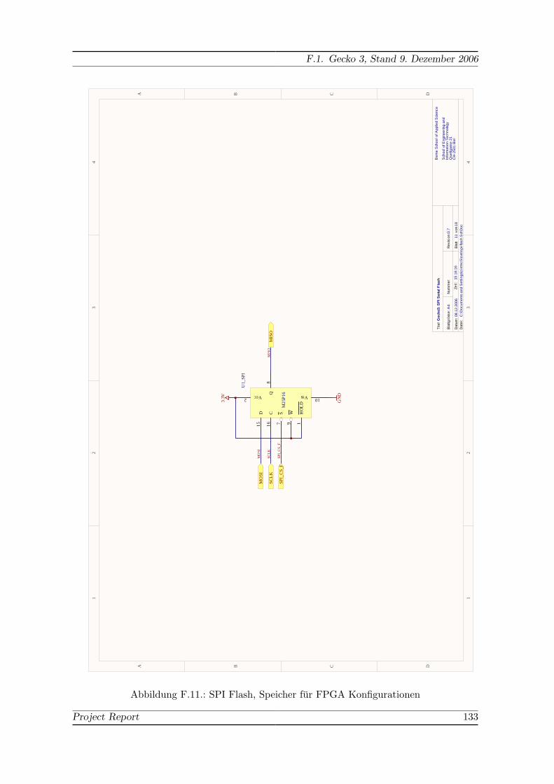
F.1. Gecko 3, Stand 9. Dezember 2006
11
22
33
44
DD
CC
BB
AA
11
Ber
ne S
choo
l of A
pplie
d S
cien
ce
Sch
ool o
f Eng
inee
ring
and
Info
rmat
ion
Tech
nolo
gyQ
uellg
asse
21
CH
-250
1 Bi
el18
Gec
ko3:
SP
I Ser
ial F
lash
0.7
08.1
2.20
0615
:16:
16C
:\Doc
umen
ts a
nd S
ettin
gs\z
imm
c5\s
vn\s
pi-f
lash
.Sch
Doc
Tite
l
Bla
ttgrö
sse:
Num
mer
:
Dat
um:
Dat
ei:
Rev
isio
n:
Bla
ttvo
nZe
it:
A4
S7
C16
D15
W9
HO
LD
1
Q8
Vcc2 Vss 10
M25
P16
U1_
SPI
GN
D
3.3V
MO
SI
SCLK
MIS
O
SPI_
CS_
F
MO
SI
SPI_
CS_
F
SCL
KM
ISO
Abbildung F.11.: SPI Flash, Speicher fur FPGA Konfigurationen
Project Report 133

F. Schemas
11
22
33
44
DD
CC
BB
AA
GR
UE
ND1_
SWA
RO
T
D1_
SWB
RO
T
D3_
SWB
GR
UE
ND2_
SWA
RO
T
D2_
SWB
GR
UE
ND4_
SWA
RO
T
D4_
SWB
Res
et B
utto
n
S4_S
W
But
ton2
S3_S
W
But
ton1
S2_S
W
But
ton0
S1_S
W
1234 5
678
S5_S
W
3.3V
LED
[0..7
]
12
Ber
ne S
choo
l of A
pplie
d S
cien
ce
Sch
ool o
f Eng
inee
ring
and
Info
rmat
ion
Tech
nolo
gyQ
uellg
asse
21
CH
-250
1 Bi
el18
Gec
ko3:
Sw
itche
s an
d LE
Ds
0.8
08.1
2.20
0614
:56:
55C
:\Doc
umen
ts a
nd S
ettin
gs\z
imm
c5\s
vn\s
witc
hes.
SchD
oc
Tite
l
Bla
ttgrö
sse:
Num
mer
:
Dat
um:
Dat
ei:
Rev
isio
n:
Bla
ttvo
nZe
it:
A4
GN
D
4.7K
R9_
SW
GN
DG
ND
220
R1_
SW
330
R2_
SW
220
R3_
SW
330
R4_
SW
220
R5_
SW
330
R6_
SW
220
R7_
SW
330
R8_
SW
But
ton0
But
ton1
But
ton2
Res
et
Switc
h0Sw
itch1
Switc
h2Sw
itch3
4.7K
R10
_SW
4.7K
R11
_SW
4.7K
R12
_SW
4.7K
R13_SW
4.7K
R14_SW
4.7K
R15_SW
4.7K
R16_SW
But
ton[
0..2
]
Switc
h[0.
.3]
LED
0
LED
1
LED
2
LED
3
LED
4
LED
5
LED
6
LED
7
GR
UE
ND3_
SWA
LED
[0..7
]
But
ton[
0..2
]
Switc
h[0.
.3]
3.3V
Res
etR
eset
Abbildung F.12.: Schalter, Taster und LEDs
134 Christoph Zimmermann

F.1. Gecko 3, Stand 9. Dezember 2006
11
22
33
44
55
66
77
88
DD
CC
BB
AA
3.3V
Uba
tt
GN
D
220u
FC
2_IO
Vbu
s
PWM[0..7]
GPIO1_[0..59]
eBot ChassisM
LB
-160
808-
S600
Q
FB2_
IO
ML
B-1
6080
8-S6
00Q
FB1_
IO
GN
D
Encoder[0..7]
Sensors[0..5]
GPIO1_[0..59]
PWM[0..7]
Encoder[0..7]
Sensors[0..5]
GN
D
PWM0PWM1PWM2PWM3PWM4PWM5PWM6PWM7
Encoder0Encoder1Encoder2Encoder3Encoder4Encoder5Encoder6Encoder7
Sensors0Sensors1Sensors2Sensors3
Sensors4Sensors5
GPIO1_0
Power Good
Low Battery
Low Battery
Low Battery
Power Good
Power Good
Vbu
s
220u
FC
1_IO
13
Ber
ne S
choo
l of A
pplie
d S
cien
ce
Sch
ool o
f Eng
inee
ring
and
Info
rmat
ion
Tech
nolo
gyQ
uellg
asse
21
CH
-250
1 Bi
el18
Gec
ko3:
Po
wer
and
I/O
Bus
0.8
08.1
2.20
0614
:56:
04C
:\Doc
umen
ts a
nd S
ettin
gs\z
imm
c5\s
vn\io
-bus
.Sch
Doc
Tite
l
Bla
ttgrö
sse:
Num
mer
:
Dat
um:
Dat
ei:
Rev
isio
n:
Bla
ttvo
nZe
it:
A3
123579111315171921232527293133353739414345474951535557596163656769717375777981838587899193959799
468
101214161820222426283032343638404244464850525456586062646668707274767880828486889092949698
100101102103104105106107108109110111112113114115116117118119120
AMP-FH-120-RECEPTABLE-H9-H13
fh-1
20r
top
JP2_IO
123579111315171921232527293133353739414345474951535557596163656769717375777981838587899193959799
468
101214161820222426283032343638404244464850525456586062646668707274767880828486889092949698
100101103105107109111113115117119
102104106108110112114116118120
AMP-FH-120-Plug
bottom
fh-1
20p
JP1_IO
VbusVbus
Ubatt
3.3V 3.3V
Ubatt
GPIO1_1GPIO1_2GPIO1_3GPIO1_4GPIO1_5GPIO1_6GPIO1_7GPIO1_8GPIO1_9GPIO1_10GPIO1_11GPIO1_12GPIO1_13GPIO1_14GPIO1_15GPIO1_16GPIO1_17GPIO1_18GPIO1_19GPIO1_20GPIO1_21GPIO1_22GPIO1_23GPIO1_24GPIO1_25
GPIO1_26GPIO1_27GPIO1_28GPIO1_29GPIO1_30GPIO1_31
GPIO1_32GPIO1_33GPIO1_34GPIO1_35GPIO1_36GPIO1_37GPIO1_38GPIO1_39GPIO1_40GPIO1_41GPIO1_42GPIO1_43GPIO1_44GPIO1_45GPIO1_46GPIO1_47GPIO1_48GPIO1_49GPIO1_50GPIO1_51GPIO1_52GPIO1_53GPIO1_54GPIO1_55GPIO1_56GPIO1_57GPIO1_58GPIO1_59
GN
DPWM0PWM1PWM2PWM3PWM4PWM5PWM6PWM7
Encoder0Encoder1Encoder2Encoder3Encoder4Encoder5Encoder6Encoder7
Sensors0Sensors1Sensors2Sensors3
Sensors4Sensors5
GPIO1_0
Low BatteryPower Good
VbusVbus
Ubatt
3.3V 3.3V
Ubatt
GPIO1_1GPIO1_2GPIO1_3GPIO1_4GPIO1_5GPIO1_6GPIO1_7GPIO1_8GPIO1_9GPIO1_10GPIO1_11GPIO1_12GPIO1_13GPIO1_14GPIO1_15GPIO1_16GPIO1_17GPIO1_18GPIO1_19GPIO1_20GPIO1_21GPIO1_22GPIO1_23GPIO1_24GPIO1_25
GPIO1_26GPIO1_27GPIO1_28GPIO1_29GPIO1_30GPIO1_31
GPIO1_32GPIO1_33GPIO1_34GPIO1_35GPIO1_36GPIO1_37GPIO1_38GPIO1_39GPIO1_40GPIO1_41GPIO1_42GPIO1_43GPIO1_44GPIO1_45GPIO1_46GPIO1_47GPIO1_48GPIO1_49GPIO1_50GPIO1_51GPIO1_52GPIO1_53GPIO1_54GPIO1_55GPIO1_56GPIO1_57GPIO1_58GPIO1_59
Abbildung F.13.: Erweiterungsbus, 1. Teil
Project Report 135

F. Schemas
11
22
33
44
55
66
77
88
DD
CC
BB
AA
SDA_ext
DREQ[1..2]
Reset
MD[0..31]
Col
ibri
bus
or u
sed
as G
PIO
GPIO2[0..34]
GPIO2_0
MA[0..25]
DQM[0..3]
123579111315171921232527293133353739414345474951535557596163656769717375777981838587899193959799
468
101214161820222426283032343638404244464850525456586062646668707274767880828486889092949698
100101102103104105106107108109110111112113114115116117118119120
AMP-FH-120-RECEPTABLE-H9-H13
fh-1
20r
top
JP1_IO2
123579111315171921232527293133353739414345474951535557596163656769717375777981838587899193959799
468
101214161820222426283032343638404244464850525456586062646668707274767880828486889092949698
100101103105107109111113115117119
102104106108110112114116118120
AMP-FH-120-Plug
bottom
fh-1
20p
JP2_IO2
GN
D
MD0MD1MD2MD3MD4MD5MD6MD7MD8MD9MD10MD11MD12MD13MD14MD15MD16MD17MD18MD19MD20MD21MD22MD23MD24MD25MD26MD27MD28MD29MD30MD31
MA0MA1MA2MA3MA4MA5MA6MA7MA8MA9MA10MA11MA12MA13MA14MA15MA16MA17MA18MA19MA20MA21MA22MA23MA24MA25
DREQ1DREQ2
DQM0DQM1DQM2DQM3
nOEnWERDnWR
nCS1RDY
nCS3nCS4
GPIO2_1GPIO2_2GPIO2_3GPIO2_4GPIO2_5GPIO2_6GPIO2_7GPIO2_8GPIO2_9GPIO2_10GPIO2_11GPIO2_12GPIO2_13GPIO2_14GPIO2_15GPIO2_16GPIO2_17
SDA_extSCL_ext
SCL_ext
GPIO2[0..34]
14
Ber
ne S
choo
l of A
pplie
d S
cien
ce
Sch
ool o
f Eng
inee
ring
and
Info
rmat
ion
Tech
nolo
gyQ
uellg
asse
21
CH
-250
1 Bi
el18
Gec
ko3:
Sys
tem
an
d I/O
Bu
s
0.7
08.1
2.20
0615
:15:
51C
:\Doc
umen
ts a
nd S
ettin
gs\z
imm
c5\s
vn\io
-bus
2.S
chD
oc
Tite
l
Bla
ttgrö
sse:
Num
mer
:
Dat
um:
Dat
ei:
Rev
isio
n:
Bla
ttvo
nZe
it:
A3
RDYnCS1nCS3nCS4RDnWRnWE
DREQ[1..2]
MD[0..31]
MA[0..25]
DQM[0..3]
nOEnWERDnWRnCS4nCS3nCS1RDY
nOE
I2C
EXTCLK0EXTCLK1
EXTCLK0EXTCLK1EXTCLK0
EXTCLK1
GPIO2_18GPIO2_19GPIO2_20GPIO2_21GPIO2_22GPIO2_23GPIO2_24GPIO2_25GPIO2_26GPIO2_27GPIO2_28GPIO2_29GPIO2_30GPIO2_31GPIO2_32GPIO2_33
Reset
SCL_extSDA_ext
GPIO2_0
MD0MD1MD2MD3MD4MD5MD6MD7MD8MD9MD10MD11MD12MD13MD14MD15MD16MD17MD18MD19MD20MD21MD22MD23MD24MD25MD26MD27MD28MD29MD30MD31
MA0MA1MA2MA3MA4MA5MA6MA7MA8MA9MA10MA11MA12MA13MA14MA15MA16MA17MA18MA19MA20MA21MA22MA23MA24MA25
DREQ1DREQ2
DQM0DQM1DQM2DQM3
nOEnWERDnWR
nCS1RDY
nCS3nCS4
GPIO2_1GPIO2_2GPIO2_3GPIO2_4GPIO2_5GPIO2_6GPIO2_7GPIO2_8GPIO2_9GPIO2_10GPIO2_11GPIO2_12GPIO2_13GPIO2_14GPIO2_15GPIO2_16GPIO2_17
SDA_extSCL_ext
EXTCLK0EXTCLK1
GPIO2_18GPIO2_19GPIO2_20GPIO2_21GPIO2_22GPIO2_23GPIO2_24GPIO2_25GPIO2_26GPIO2_27GPIO2_28GPIO2_29GPIO2_30GPIO2_31GPIO2_32GPIO2_33
Reset Reset
GN
D
Abbildung F.14.: Erweiterungsbus, 2. Teil
136 Christoph Zimmermann

F.1. Gecko 3, Stand 9. Dezember 2006
11
22
33
44
DD
CC
BB
AA
GN
D
1.2V
2.5V
Uba
tt
22uF
C7_
PWR
22uF
C5_
PWR
GN
D
GN
D
2.2M
R1_
PWR
1nF
X7R
C1_
PWR
180K
R2_
PWR
82K
R5_
PWR
160K
R4_
PWR
22pF
X5R
C6_
PWR
GN
D
GN
D
GN
D6.2K
R3_
PWR
1nF
X7R
C3_
PWR
22pF
C2_
PWR
15
Ber
ne S
choo
l of A
pplie
d S
cien
ce
Sch
ool o
f Eng
inee
ring
and
Info
rmat
ion
Tech
nolo
gyQ
uellg
asse
21
CH
-250
1 Bi
el18
Gec
ko3:
Pow
er S
uplie
s
0.7
08.1
2.20
0614
:56:
39C
:\Doc
umen
ts a
nd S
ettin
gs\z
imm
c5\s
vn\p
ower
.SC
HD
OC
Tite
l
Bla
ttgrö
sse:
Num
mer
:
Dat
um:
Dat
ei:
Rev
isio
n:
Bla
ttvo
nZe
it:
A4
DC
/DC
Con
verte
r for
the
FPG
A C
ore S
uppl
y, 1
.2 V
, 2.5
A
3.3V
GN
D
Bul
k C
apac
itor f
or b
oth
Flas
h C
hips
100
R6_
PWR
100
R7_
PWR
2.5V
GN
D
Vre
f
100n
FC
8_PW
R
GN
DG
ND
100n
FC
9_PW
R
1nF
C4_
PWR G
ND
3.3V
GN
DG
ND
GN
D
TP1
_PW
R
GN
D
2.5
V, 0
.5 A
and
1.25
V R
efer
nce
Supp
lyG
ND
Tes
tpad
for P
robe
s
RT
15
Run
/SS
1
Ith
13
Sync
/Mod
e16
Vfb
14
SGND 2
PGND 7Pg
ood
12PVin3
SVin11
SW4
PVin10
SW5
SW8
SW9
PGND 6
SGND 17
LTC
3412
AU
1_PW
R
GND 4
IN3
OU
T1
LP8
340C
DT
-2.5
U2_
PWR
10uF
C12
_PW
R2.
2uF
C11
_PW
R
10uF
C10
_PW
R
2uH
SD14
-2R
0-R
L1_
PWR
Abbildung F.15.: Spannungsversorgung
Project Report 137

F. Schemas
11
22
33
44
DD
CC
BB
AA
1 2 3 4 5 6
Hea
der 1
x6, r
ight
ang
le
JP1_
JTA
G
JTA
G C
onne
ctor
GN
D
TDI
TDO
TCK
TMS
for t
he D
igile
nt P
rogr
amm
ing
Cab
le
16
Ber
ne S
choo
l of A
pplie
d S
cien
ce
Sch
ool o
f Eng
inee
ring
and
Info
rmat
ion
Tech
nolo
gyQ
uellg
asse
21
CH
-250
1 Bi
el18
Gec
ko3:
Jta
g an
d R
S23
2 C
onne
cto
r
0.7
08.1
2.20
0615
:45:
01C
:\Doc
umen
ts a
nd S
ettin
gs\z
imm
c5\s
vn\jt
ag.S
chD
oc
Tite
l
Bla
ttgrö
sse:
Num
mer
:
Dat
um:
Dat
ei:
Rev
isio
n:
Bla
ttvo
nZe
it:
A4
100
R2_
JTA
G3.
3V10
0R
3_JT
AG
100
R1_
JTA
GT
CK
TD
IT
MS
TD
O
1234
JP2_
JTA
G
GN
D3.3V
Seri
al o
ut
Seri
al in
Con
nect
or fo
r se
rial
com
mun
icat
ion
Abbildung F.16.: JTAG Anschluss
138 Christoph Zimmermann
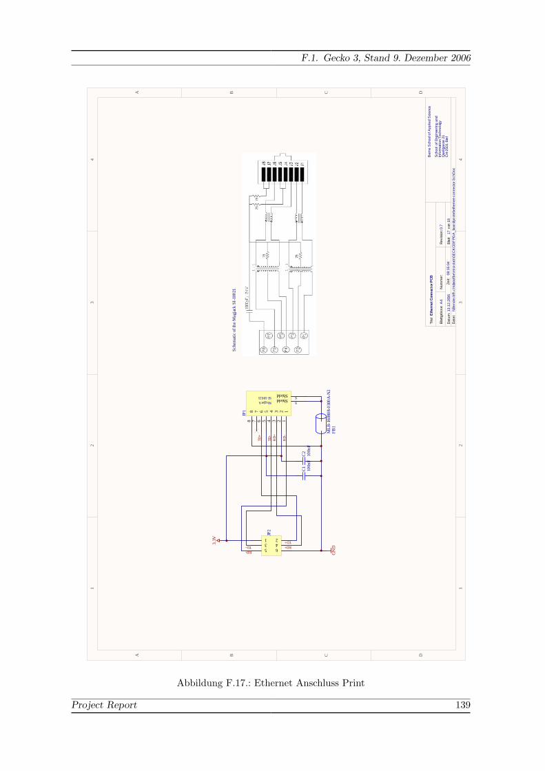
F.1. Gecko 3, Stand 9. Dezember 2006
11
22
33
44
DD
CC
BB
AA
3.3V
Sche
mat
ic o
f the
Mag
jack
SI-
1002
1
GN
DTD-TD+
RD-RD+
MLB
-160
808-
0300
A-N
2FB
1
RD
-
RD
+TD
-
TD+
17
Ber
ne S
choo
l of A
pplie
d S
cien
ce
Sch
ool o
f Eng
inee
ring
and
Info
rmat
ion
Tec
hnol
ogy
Que
llgas
se 2
1C
H-2
501
Bie
l18
Eth
erne
t Con
nec
tor P
CB
0.7
13.1
2.20
0608
:35:
04\\B
lend
er.b
fh.c
h\da
ta\fb
e\m
icro
lab\
GE
CK
O3\
FPG
A_b
oard
\pro
tel\e
ther
net-c
onne
ctor
.Sch
Doc
Tite
l
Bla
ttgrö
sse:
Num
mer
:
Dat
um:
Dat
ei:
Rev
isio
n:
Bla
ttvo
nZe
it:
A4
100n
FC
110
0nF
C2
1 23 45 6
JP2
11
88
77
66
55
44
33
22
Magjack Shield s
Shield sSI-10021
JP1
Abbildung F.17.: Ethernet Anschluss Print
Project Report 139
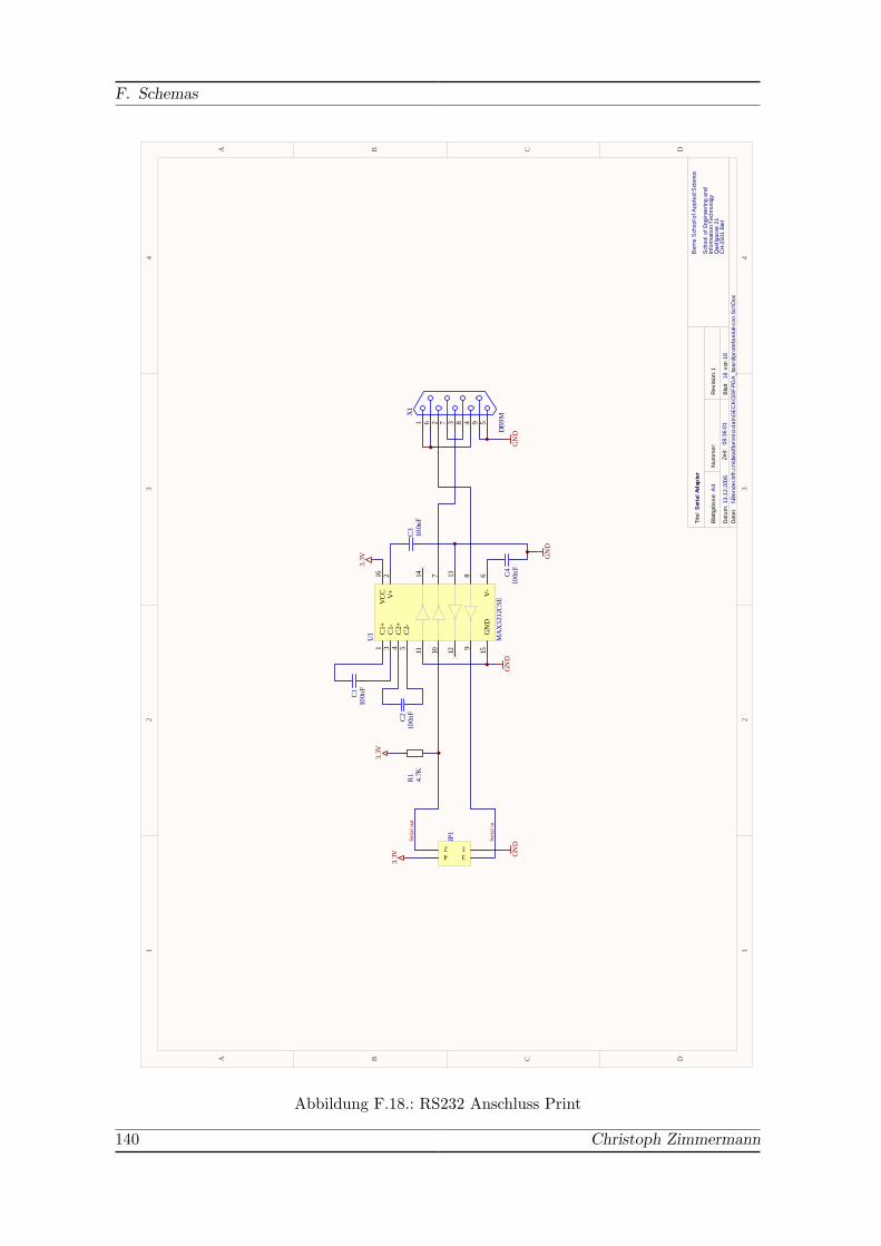
F. Schemas
11
22
33
44
DD
CC
BB
AA
18
Ber
ne S
choo
l of A
pplie
d S
cien
ce
Sch
ool o
f Eng
inee
ring
and
Info
rmat
ion
Tec
hnol
ogy
Que
llgas
se 2
1C
H-2
501
Bie
l18
Ser
ial A
dap
ter
1
13.1
2.20
0608
:36:
01\\B
lend
er.b
fh.c
h\da
ta\fb
e\m
icro
lab\
GE
CK
O3\
FPG
A_b
oard
\pro
tel\s
eria
l-con
.Sch
Doc
Tite
l
Bla
ttgrö
sse:
Num
mer
:
Dat
um:
Dat
ei:
Rev
isio
n:
Bla
ttvo
nZe
it:
A4
13
1011
8
12 9
14 7
C1+
1
C2+
4
GN
D15
C1-
3V
CC
16
C2-
5
V-
6
V+
2
MA
X32
32C
SE
U1
1 6 2 7 3 8 4 9 5
DB
9M
X1
1234
JP1
GN
D
3.3V
4.7K
R1
100n
FC
1
GN
DG
ND
Seria
l out
Seria
l in
3.3V
100n
FC
2
100n
FC
4
GN
D
100n
FC
3
3.3V
Abbildung F.18.: RS232 Anschluss Print
140 Christoph Zimmermann
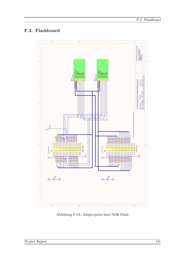
F.2. Flashboard
F.2. Flashboard
11
22
33
44
DD
CC
BB
AA
Flas
h_D
Q[0
..15]
Flas
h_A
[0..2
3]Fl
ash_
BY
TEFl
ash_
WE
Flas
h_R
PFl
ash_
OE
Flas
h_C
E0
flash
flash
.Sch
Doc
1
Ber
ne S
choo
l of A
pplie
d S
cien
ce
Sch
ool o
f Eng
inee
ring
and
Info
rmat
ion
Tec
hnol
ogy
Que
llgas
se 2
1C
H-2
501
Bie
l1
Flas
h M
emor
y B
oar
d fo
r the
Sp
arta
n3 D
evel
opm
entb
oard
0.2
08.1
2.20
0617
:51:
37C
:\Doc
umen
ts a
nd S
ettin
gs\z
imm
c5\fl
ash-
boar
d\fla
shbo
ard.
Sch
Doc
Tite
l
Bla
ttgrö
sse:
Num
mer
:
Dat
um:
Dat
ei:
Rev
isio
n:
Bla
ttvo
nZe
it:
A4
12
34
56
78
910
1112
1314
1516
1718
1920
2122
2324
2526
2728
2930
3132
3334
3536
3738
3940
Hea
der
20X
2
Con
nect
or: A
1
JP1 1
23
45
67
89
1011
1213
1415
1617
1819
2021
2223
2425
2627
2829
3031
3233
3435
3637
3839
40
Hea
der
20X
2
Con
nect
or: A
2
JP2
Flas
h_D
Q[0
..15]
Flas
h_A
[0..2
3]Fl
ash_
BY
TEFl
ash_
WE
Flas
h_R
PFl
ash_
OE
Flas
h_C
E0
flash
flash
.Sch
Doc
Bus
y
X1
Flas
h_W
EFl
ash_
OE
Flas
h_BY
TE
Flas
h_RP
Flas
h_CE
0 GN
D
3.3V G
ND
3.3V
with
this
boar
d yo
u ca
n't u
se th
e se
cond
osc
ilato
r!
3.3V
GN
D10uF
C4
3.3V
GN
D10uF
C5
Flas
h1_D
Q0
Flas
h1_D
Q1
Flas
h1_D
Q2
Flas
h1_D
Q3
Flas
h1_D
Q4
Flas
h1_D
Q5
Flas
h1_D
Q6
Flas
h1_D
Q7
Flas
h1_D
Q8
Flas
h1_D
Q9
Flas
h1_D
Q10
Flas
h1_D
Q11
Flas
h1_D
Q12
Flas
h1_D
Q13
Flas
h1_D
Q14
Flas
h1_D
Q15
Flas
h2_D
Q0
Flas
h2_D
Q1
Flas
h2_D
Q2
Flas
h2_D
Q3
Flas
h2_D
Q4
Flas
h2_D
Q5
Flas
h2_D
Q6
Flas
h2_D
Q7
Flas
h2_D
Q8
Flas
h2_D
Q9
Flas
h2_D
Q10
Flas
h2_D
Q11
Flas
h2_D
Q12
Flas
h2_D
Q13
Flas
h2_D
Q14
Flas
h2_D
Q15
Flas
h1_D
Q[0
..15]
Flas
h2_D
Q[0
..15]
Flas
h_A
ddr[0
..23]
Flas
h_A
ddr[0
..23]
Flas
h_A
ddr0
Flas
h_A
ddr1
Flas
h_A
ddr2
Flas
h_A
ddr3
Flas
h_A
ddr4
Flas
h_A
ddr5
Flas
h_A
ddr6
Flas
h_A
ddr7
Flas
h_A
ddr8
Flas
h_A
ddr9
Flas
h_A
ddr1
0Fl
ash_
Add
r11
Flas
h_A
ddr1
2Fl
ash_
Add
r13
Flas
h_A
ddr1
4Fl
ash_
Add
r15
Flas
h_A
ddr1
6Fl
ash_
Add
r17
Flas
h_A
ddr1
8Fl
ash_
Add
r19
Flas
h_A
ddr2
0Fl
ash_
Add
r21
Flas
h_A
ddr2
2Fl
ash_
Add
r23
Abbildung F.19.: Adapterprint Intel NOR Flash
Project Report 141
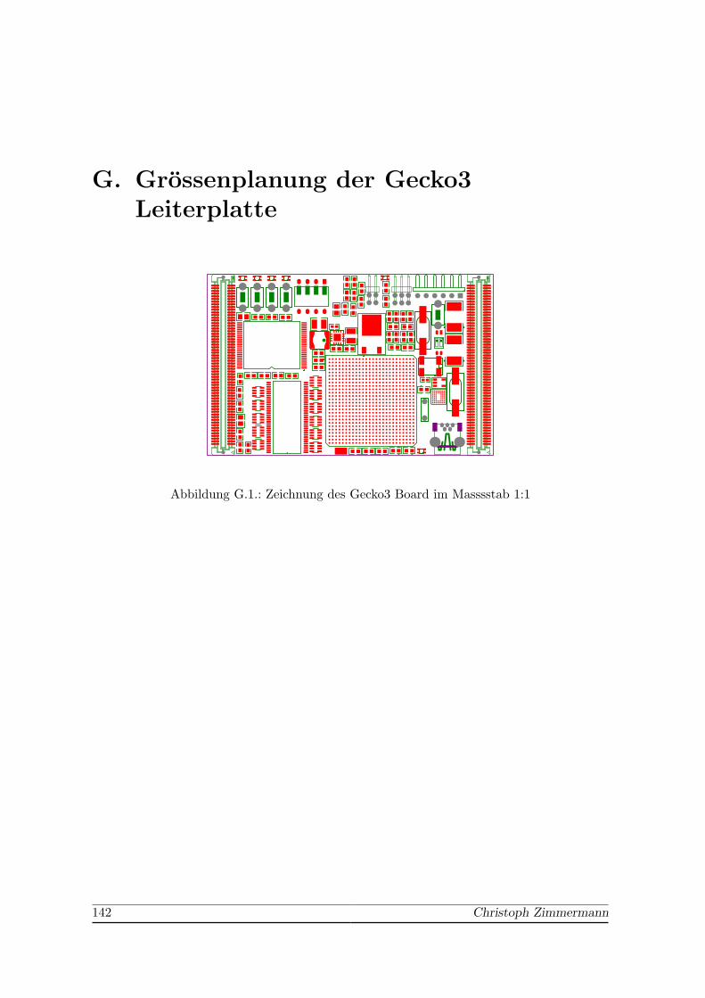
G. Grossenplanung der Gecko3Leiterplatte
Abbildung G.1.: Zeichnung des Gecko3 Board im Masssstab 1:1
142 Christoph Zimmermann
Literaturverzeichnis
[Bre03] Ulrich Breymann. C++ Einfuhrung und professionelle Programmierung. Hanser,2003.
[Cad00] Gerhard R. Cadek. Digital Design Guidelines for FPGA Design. ArbeitsgruppeCAD - Institut fur Computertechnik - TU Wien, May 2000.
[Cyp03] Cypress Semiconductor Corporation, 3901 North First Street San Jose, CA 95134.EZ-USB FX2 GPIF Primer, April 2003.
[Cyp06] Cypress. EZ-USB Technical Reference Manual. Cypress, 2006.
[Hyd99] John Hyde. USB Desing by Example (A practical Guide to building I/O Devices).Intel, 1999.
[Jac] Dr. Marcel Jacomet. VLSI System Design. Berne School of Applied Sciences.
[Mic] Microchip. I2C CMOS Serial EEPROM.
[NP02] Mark Ng and Mike Peattie. Using a Microprocessor to Configure Xilinx FPGAs viaSlave Serial or SelectMAP Mode. Xilinx, November 2002.
[Sch03] J. Reichardt/ B. Schwarz. VHDL-Synthese. Oldenbourg, 2003.
[Tse04] Chen Wei Tseng. Spartan-3 Advanced Configuration Architecture. Xilinx, Inc, 1.0edition, December 2004.
Project Report 143