gan fet-based high ccm totem-pole bridgeless pfc psds ... · totem-pole bridgeless pfc + good...
TRANSCRIPT
GaN FET-Based High CCM Totem-Pole Bridgeless PFC
Zhong Ye
Alvaro Aguilar Yitzhak Bolurian Brian Daugherty

Agenda
6-2
• AC/DC efficiency standard and PFC efficiency requirement
• Bridgeless PFC topologies and development trend
• GaN ( Gallium Nitride) FET overview
• Totem-pole CCM bridgeless PFC control - UCD3138 control implementation - Ideal diode emulation - AC crossover detection and control
• GaN device test in FET mode and diode mode
• Totem-pole CCM bridgeless PFC test
• Summary
Texas Instruments – 2014/15 Power Supply Design Seminar

AC/DC Efficiency Level Certifications
6-3 Texas Instruments – 2014/15 Power Supply Design Seminar
80 Plus Test Type
115 V Internal Non-Redundant
230 V Internal Redundant
Fraction of rated load
10% 20% 50% 100% 10% 20% 50% 100%
80 Plus 80% 80% 80% 80 Plus Bronze 82% 85% 82% 81% 85% 81% 80 Plus Silver 85% 88% 85% 85% 89% 85% 80 Plus Gold 87% 90% 87% 88% 92% 88% 80 Plus Platinum 90% 92% 89% 90% 94% 91% 80 Plus Titanium 90% 92% 94% 90% 90% 94% 96% 91%
Energy Star Specification

PFC Efficiency Budget
Texas Instruments – 2014/15 Power Supply Design Seminar 6-4
• PFC design becomes more challenging at Platinum level efficiency and much harder at Titanium level efficiency
• Well designed single-phase PFC and interleaved PFC achieve around 97.5% efficiency and are just able to meet Platinum efficiency requirement
• Bridgeless seems to be the only way to reach Titanium efficiency level
80 Plus Test Type
Efficiency at 115 V Internal Non-Redundant
Efficiency at 230 95.5%V Internal Redundant
Fraction of rated load 10% 20% 50% 100% 10% 20% 50% 100%
80 Plus Platinum
PFC 95.8% 95.4% 93.7% 95.7% 97.4% 95.8%
DC/DC 94% 96.5% 95% 94% 96.5% 95%
80 Plus Titanium
PFC 95.5% 95.8% 96.4% 93.8% 95.8% 98% 98.5% 94.8%
DC/DC 94% 96% 97.5% 96% 94% 96% 97.5% 96%

6-5
Existing Bridgeless PFC Application Status Basic Bridgeless PFC + Good efficiency
+ Easy control
- High component count
- Low component utilization
- Low density
Totem-Pole Bridgeless PFC + Good efficiency
+ Fixed frequency
+ Easy control
- DCM only
- For power < 300 W
Texas Instruments – 2014/15 Power Supply Design Seminar
D1
Q1
D2
Q2
D5
D5
D3
D4
+
-
COC1
C2 C3 C4
L2
Lb1
Lb2
Lb
Q1
Q2
D1
D2
D3
D4
+
-
COC1
C2 C3 C4
L2
Line
Line/
Neutral
Earth
Line
Line/
Neutral
Earth

6-6
New PFC Development Trends
Texas Instruments – 2014/15 Power Supply Design Seminar
Transition-Mode Totem-Pole PFC • ZVS operation • Interleaved configuration for high power application (around max 300 W per phase) • Variable frequency control • Phase shedding and adding to optimize light load efficiency • Suitable for MOSFET applications Continuous-Conduction-Mode Totem-Pole PFC • Low component count • Fixed switching frequency, zero reverse recovery switch should be used • GaN is a good candidate for the application • Possible to operate TM and ZVS at light loads
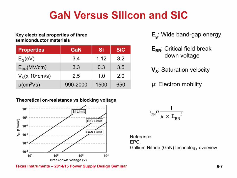
GaN Versus Silicon and SiC Eg: Wide band-gap energy EBR: Critical field break down voltage VS: Saturation velocity µ: Electron mobility
6-7 Texas Instruments – 2014/15 Power Supply Design Seminar
Properties GaN Si SiC EG(eV) 3.4 1.12 3.2 EBR(MV/cm) 3.3 0.3 3.5 VS(x 107cm/s) 2.5 1.0 2.0 µ(cm2Vs) 990-2000 1500 650
Theoretical on-resistance vs blocking voltage
101
100
10-1
10-2
10-3
10-4
101 102 103 104
RO
N �ȍ
PP
2)
Breakdown Voltage (V)
6L�/LPLW
6L&�/LPLW
*D1�/LPLWReference: EPC, Gallium Nitride (GaN) technology overview
rONα1
µ × EBR3
Key electrical properties of three semiconductor materials

100
10
1
0.1
0.01
7000
6000
5000
4000
3000
2000
1000
0
0 400 800 1200 1600 2000 2400
0 50 100 150 200
Ke
y F
igu
re
of
Me
rit
(R
ON
x Q
G�>ȍ
�Q&@
VDSS�>9@
6ZLWFKLQJ�)LJXUH�RI�0HULW�±�6L�YV��6L&�YV��*D1
}
}
1200 V GaN cascode
performance range
600/650 V GaN cascode
performance range
LV GaN FET
(Enhancement)
RF GaN FET
(Depletion)
Si FETs
GaN 66 V/µmGaN 66 V/µmSilicon transistors
6LOLFRQ *D1
6L&Cree
Infineon
ST
International Rectifier
Toshiba
6L&�&DVFRGHAOS/SemiSouth
EPC-CO
International Rectifier
Micro GaN
GaN Systems 2012 rON x QG�>ȍ x S&@R
ON
x &
OS
S�>P
ȍ x
S)@
Power Electronics Technology Feb. 2013
Figure of Merit Comparison
Figure of Merit depicts fundamental characteristics of switching devices – Rds_on, Qg, COSS and breakdown voltage
6-8 Texas Instruments – 2014/15 Power Supply Design Seminar
6-9
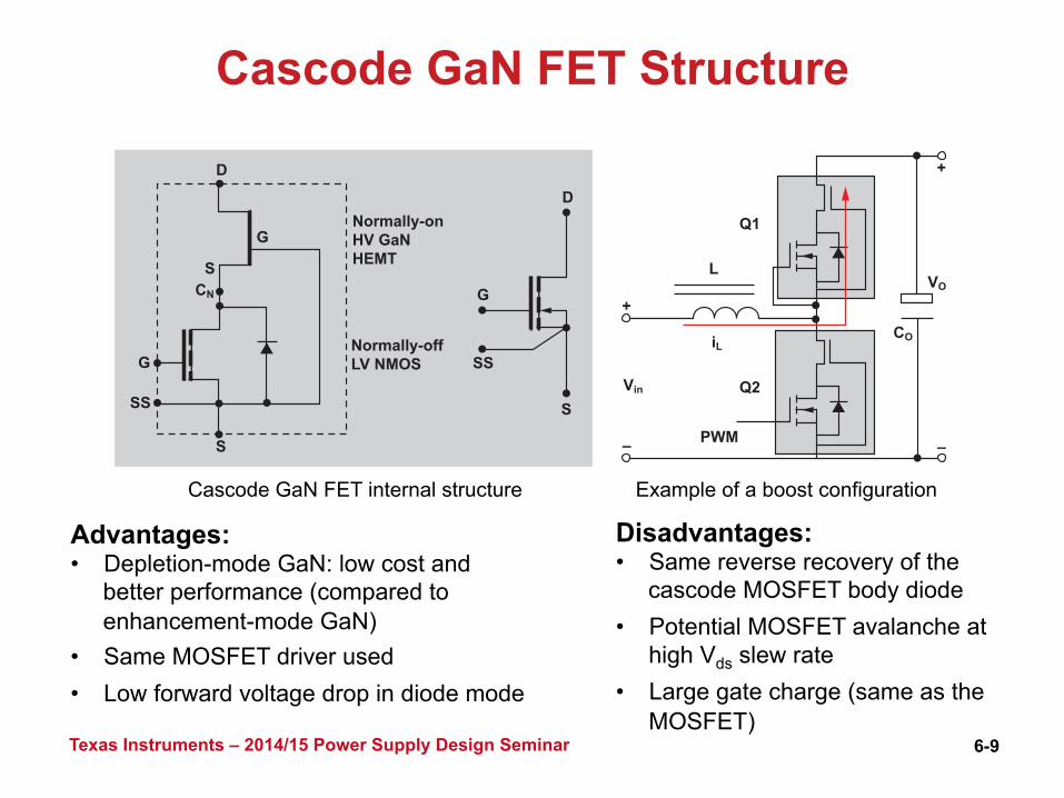
Cascode GaN FET Structure
Texas Instruments – 2014/15 Power Supply Design Seminar
Cascode GaN FET internal structure Example of a boost configuration
Advantages: • Depletion-mode GaN: low cost and
better performance (compared to enhancement-mode GaN)
• Same MOSFET driver used • Low forward voltage drop in diode mode
Disadvantages: • Same reverse recovery of the
cascode MOSFET body diode • Potential MOSFET avalanche at high Vds slew rate • Large gate charge (same as the MOSFET)
Normally-onHV GaNHEMT
Normally-offLV NMOS SS
G
D
SSS
G
D
G
S
SCN
+
–
+
–
VO
CO
Q1
Q2
L
iL
Vin
PWM

Dmode-GaN + Safety FET Structure
6-10 Texas Instruments – 2014/15 Power Supply Design Seminar
PWM
D
GND
VCC
S
Normally onHV GaN
StartupMOSFET
GateDriver
StartupLogic
Advantages: • Zero reverse recovery • Low gate charge • No LV MOSFET switching loss • Suitable for high switching frequency applications • Integrated gate driver circuit to ease applications
Disadvantages: • High forward voltage drop in
diode mode • Complicated gate driver circuit (IC design)

+
–
VO
CO
Q1
Q2
Q3
Q4
PWM
GND
VCC D
S
PWM
GND
ZCD
VCC D
S
StartupLogic
StartupLogic
IsolatedPower
DigitalISO
HallSensor
AC1
AC2
Earth
Iac
12 V
Vg3
12 V12 V
Vg1
Vg2
Vg4
Driv
er
6-11
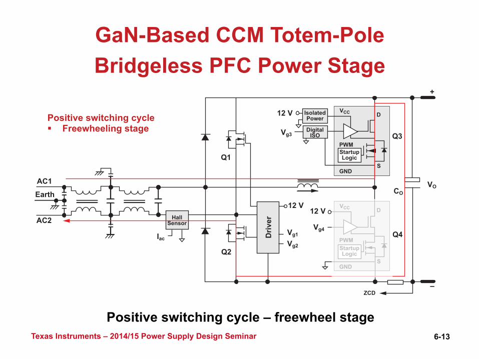
GaN-Based CCM Totem-Pole Bridgeless PFC Power Stage
Texas Instruments – 2014/15 Power Supply Design Seminar
Positive switching cycle § Active switching stage
• Q1 and Q2 are low frequency switches.
• Q3 and Q4 are an active switch and a SyncFET.

Positive switching cycle – active switching stage
6-12 Texas Instruments – 2014/15 Power Supply Design Seminar
GaN-Based CCM Totem-Pole Bridgeless PFC Power Stage
Positive switching cycle § Active switching stage
+
–
VOCO
Q1
Q2
Q3
Q4
PWM
GND
VCC D
S
PWM
GND
VCC D
S
StartupLogic
StartupLogic
IsolatedPower
DigitalISO
HallSensor
AC1
AC2
Earth
Iac
12 V
Vg3
12 V12 V
Vg1
Vg2
Vg4
Driv
er
ZCD
+
–
VOCO
Q1
Q2
Q3
Q4
PWM
GND
VCC D
S
PWM
GND
ZCD
VCC D
S
StartupLogic
StartupLogic
IsolatedPower
DigitalISO
HallSensor
AC1
AC2
Earth
Iac
12 V
Vg3
12 V12 V
Vg1
Vg2
Vg4
Driv
er
6-13 Texas Instruments – 2014/15 Power Supply Design Seminar
Positive switching cycle – freewheel stage
GaN-Based CCM Totem-Pole Bridgeless PFC Power Stage
Positive switching cycle § Freewheeling stage
+
–
+
–
VO
CO
Q3
PWM1A
PWM1B
iL
Q4
PWM
GNDL
VCC
VCC
D
S
PWM
GND
D
S
Startup
Logic
Startup
Logic
100
80
60
40
20
0
-20
-40
-60
-80
-100
-3.0 -2.0 -1.0 0 1.0 2.0 3.0
VD
VGS
I D
0 V
-1 V
-1.5 V
-2 V
-2.5 V
-3.3 V
VDS of Q3
-iQ3iQ4 -iQ3iQ4
Vg of Q4
VDS of Q3
Vg of Q4 Vg of Q3
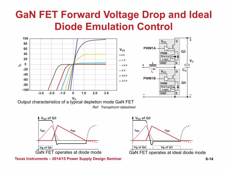
GaN FET Forward Voltage Drop and Ideal Diode Emulation Control
6-14 Texas Instruments – 2014/15 Power Supply Design Seminar
Output characteristics of a typical depletion mode GaN FET Ref: Transphorm datasheet
GaN FET operates at diode mode GaN FET operates at ideal diode mode
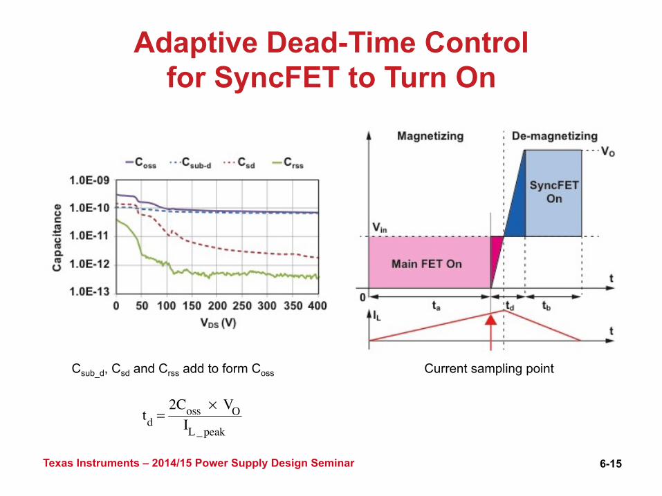
Adaptive Dead-Time Control for SyncFET to Turn On
6-15 Texas Instruments – 2014/15 Power Supply Design Seminar
Csub_d, Csd and Crss add to form Coss Current sampling point
td =2Coss × VO
IL_peak
Da Db Da Db Da DaDb
DbDa Da
ZCD
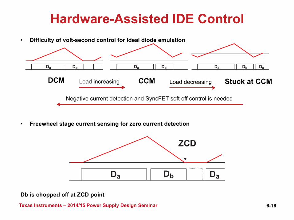
Hardware-Assisted IDE Control
6-16 Texas Instruments – 2014/15 Power Supply Design Seminar
• Difficulty of volt-second control for ideal diode emulation
CCM Load increasing Stuck at CCM
Negative current detection and SyncFET soft off control is needed
• Freewheel stage current sensing for zero current detection
Db is chopped off at ZCD point
DCM Load decreasing

UDC3138 Digital Controller
Q3 Q4Q2Q1
VO
Vref
Iref
AB
C
+
-+
-
IS
SyncFET
Programmable NCD Ref
Main FET
Comparator
Iac
AC1
AC2
Current Loop
Voltage Loop
Main FET and SyncFET
Selection
EADC + CLA + DPWM
GVKmABC
ZCD
1/Vrms2Vrms
Kf|x|ADC
ADC
Crossover
Detection
UCD3138 – Based Control Circuit
6-17 Texas Instruments – 2014/15 Power Supply Design Seminar

Test Results – GaN FET Performance in FET Mode
6-18 Texas Instruments – 2014/15 Power Supply Design Seminar
Test Conditions: • Vin = 200 VDC, Iin = 2 ADC, VO = 400 V • Q4: 600 V 150 mΩ depletion-mode GaN power transistor • D3: Cree SiC diode C3D04060A • Gate turn-off resistance = 2.2 Ω, turn-on resistance=15 Ω Test Results: • Turn-on time = 9 nS • Max turn-on dV/dt = 79 V/nS • Coss is linearly charged up to VO at turn-off • About 18 V ringing when freewheel diode conducts
+
–
VO
CO
Q3
Q4
SiC
D3
PWM
GND
VCCD
S
Startup
Logic
12 V
Vg4Vin
+
–
IL

6-19 Texas Instruments – 2014/15 Power Supply Design Seminar
Test Results – GaN FET Forward Voltage Drop in Diode Mode
Test Conditions: • Current = 0.1 A – 3 A, dead-time = 100 nS Test Results: • Forward voltage drop varies from 4.3 V to 7.3 V device-to-device when GaN is off
+
–
VO
CO
Q3
Q4
PWM
GND
VCCD
S
PWM
GND
VCCD
S
Startup
Logic
Startup
Logic
Isolated
Power
Digital
ISO
12 V
Vg3
12 V
Vg4
Vin
+
–
IL
GaN
Si: STTH8R06D
SiC
+
–
VO
CO
Q3
Q4
PWM
GND
VCC D
S
PWM
GND
VCC D
S
StartupLogic
StartupLogic
IsolatedPower
DigitalISO
12 V
Vg3
12 V
Vg4Vin
IL
+–
6-20 Texas Instruments – 2014/15 Power Supply Design Seminar
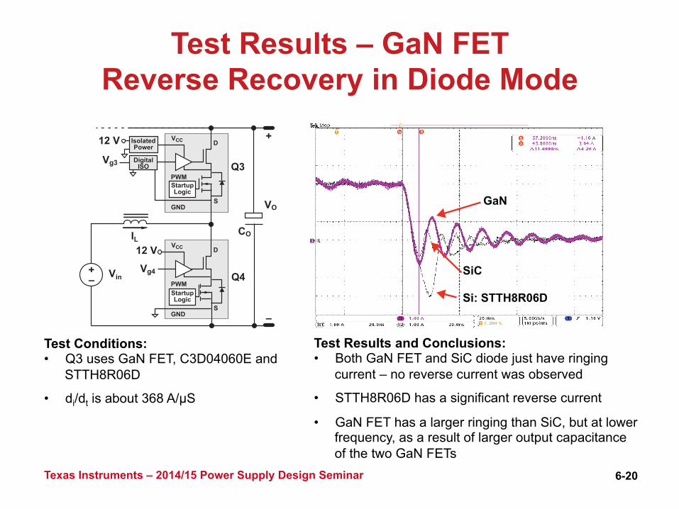
Test Results – GaN FET Reverse Recovery in Diode Mode
Test Conditions: • Q3 uses GaN FET, C3D04060E and
STTH8R06D
• di/dt is about 368 A/µS
Test Results and Conclusions: • Both GaN FET and SiC diode just have ringing
current – no reverse current was observed
• STTH8R06D has a significant reverse current
• GaN FET has a larger ringing than SiC, but at lower frequency, as a result of larger output capacitance of the two GaN FETs

6-21 Texas Instruments – 2014/15 Power Supply Design Seminar
AC Current Crossover Control
115 Vac
230 Vac|Vac_L – Vac_N|
0
|Vac|
VT_H
VT_L
Vg_Q1 Vg_Q2
Vg_Q3 Vg_Q4
RectifierFETs
ActiveGaN FETs
Integrator Running Integrator RunningIntegrator Stall
Turn-on Delay
Soft Turning On
Negative Half Cycle Positive Half Cycle

6-22 Texas Instruments – 2014/15 Power Supply Design Seminar
Current Spike Root Causes and Solutions
Root Causes: • Inaccurate a.c. voltage sensing • Turning on rectifier FET too early
cause a.c. line short sircuit • Current loop disturbed by current spike • Rectifier FET hard switching • Current loop compensation not
optimized
Solutions: • Differential a.c. voltage sensing with low
phase offset • Using different a.c. crossover voltage
thresholds for high line and low line • Sufficient blanking time • Disable PWM and stall integrator during
blanking time • Rectifier FET soft switching on • Inserting PWM turn-on delay time • Optimize current loop compensation
6-23 Texas Instruments – 2014/15 Power Supply Design Seminar
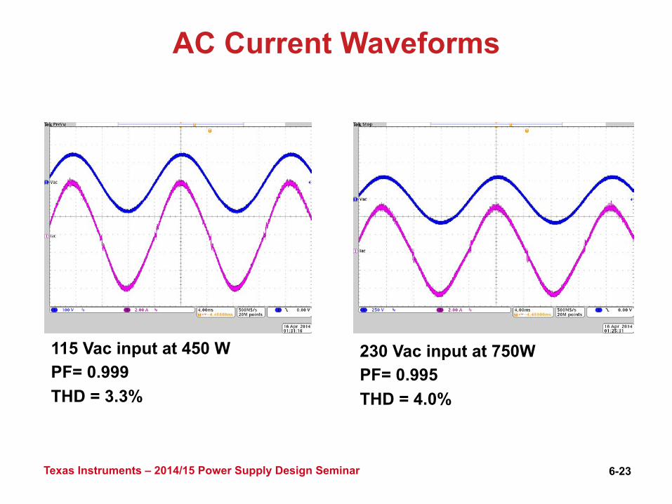
AC Current Waveforms
115 Vac input at 450 W PF= 0.999 THD = 3.3%
230 Vac input at 750W PF= 0.995 THD = 4.0%
6-24 Texas Instruments – 2014/15 Power Supply Design Seminar
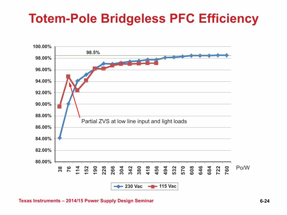
Totem-Pole Bridgeless PFC Efficiency
38 76 114
152
190
228
266
304
342
380
418
456
494
532
570
608
646
684
722
760
100.00%
98.00%
96.00%
94.00%
92.00%
90.00%
88.00%
86.00%
84.00%
82.00%
80.00%
98.5%
230 Vac 115 Vac
Partial ZVS at low line input and light loads
Po/W

6-25 Texas Instruments – 2014/15 Power Supply Design Seminar
750 W Totem-Pole Bridgeless PFC Prototype

6-26 Texas Instruments – 2014/15 Power Supply Design Seminar
Summary • GaN FET exhibits superior switching characteristics • Safety GaN FETs has zero reverse recovery
• Suitable for high-frequency hard-switching applications
• Relative high “body diode” forward drop • Sophisticated ideal-diode-emulation is the key to the success of Safety
GaN FET applications
• Enables Totem-Pole PFC CCM operation • AC crossover current spike root causes were analyzed and solutions
provided
• High efficiency potential
• Possible TM ZVS control to optimize light loads efficiency
IMPORTANT NOTICE
Texas Instruments Incorporated and its subsidiaries (TI) reserve the right to make corrections, enhancements, improvements and otherchanges to its semiconductor products and services per JESD46, latest issue, and to discontinue any product or service per JESD48, latestissue. Buyers should obtain the latest relevant information before placing orders and should verify that such information is current andcomplete. All semiconductor products (also referred to herein as “components”) are sold subject to TI’s terms and conditions of salesupplied at the time of order acknowledgment.TI warrants performance of its components to the specifications applicable at the time of sale, in accordance with the warranty in TI’s termsand conditions of sale of semiconductor products. Testing and other quality control techniques are used to the extent TI deems necessaryto support this warranty. Except where mandated by applicable law, testing of all parameters of each component is not necessarilyperformed.TI assumes no liability for applications assistance or the design of Buyers’ products. Buyers are responsible for their products andapplications using TI components. To minimize the risks associated with Buyers’ products and applications, Buyers should provideadequate design and operating safeguards.TI does not warrant or represent that any license, either express or implied, is granted under any patent right, copyright, mask work right, orother intellectual property right relating to any combination, machine, or process in which TI components or services are used. Informationpublished by TI regarding third-party products or services does not constitute a license to use such products or services or a warranty orendorsement thereof. Use of such information may require a license from a third party under the patents or other intellectual property of thethird party, or a license from TI under the patents or other intellectual property of TI.Reproduction of significant portions of TI information in TI data books or data sheets is permissible only if reproduction is without alterationand is accompanied by all associated warranties, conditions, limitations, and notices. TI is not responsible or liable for such altereddocumentation. Information of third parties may be subject to additional restrictions.Resale of TI components or services with statements different from or beyond the parameters stated by TI for that component or servicevoids all express and any implied warranties for the associated TI component or service and is an unfair and deceptive business practice.TI is not responsible or liable for any such statements.Buyer acknowledges and agrees that it is solely responsible for compliance with all legal, regulatory and safety-related requirementsconcerning its products, and any use of TI components in its applications, notwithstanding any applications-related information or supportthat may be provided by TI. Buyer represents and agrees that it has all the necessary expertise to create and implement safeguards whichanticipate dangerous consequences of failures, monitor failures and their consequences, lessen the likelihood of failures that might causeharm and take appropriate remedial actions. Buyer will fully indemnify TI and its representatives against any damages arising out of the useof any TI components in safety-critical applications.In some cases, TI components may be promoted specifically to facilitate safety-related applications. With such components, TI’s goal is tohelp enable customers to design and create their own end-product solutions that meet applicable functional safety standards andrequirements. Nonetheless, such components are subject to these terms.No TI components are authorized for use in FDA Class III (or similar life-critical medical equipment) unless authorized officers of the partieshave executed a special agreement specifically governing such use.Only those TI components which TI has specifically designated as military grade or “enhanced plastic” are designed and intended for use inmilitary/aerospace applications or environments. Buyer acknowledges and agrees that any military or aerospace use of TI componentswhich have not been so designated is solely at the Buyer's risk, and that Buyer is solely responsible for compliance with all legal andregulatory requirements in connection with such use.TI has specifically designated certain components as meeting ISO/TS16949 requirements, mainly for automotive use. In any case of use ofnon-designated products, TI will not be responsible for any failure to meet ISO/TS16949.
Products ApplicationsAudio www.ti.com/audio Automotive and Transportation www.ti.com/automotiveAmplifiers amplifier.ti.com Communications and Telecom www.ti.com/communicationsData Converters dataconverter.ti.com Computers and Peripherals www.ti.com/computersDLP® Products www.dlp.com Consumer Electronics www.ti.com/consumer-appsDSP dsp.ti.com Energy and Lighting www.ti.com/energyClocks and Timers www.ti.com/clocks Industrial www.ti.com/industrialInterface interface.ti.com Medical www.ti.com/medicalLogic logic.ti.com Security www.ti.com/securityPower Mgmt power.ti.com Space, Avionics and Defense www.ti.com/space-avionics-defenseMicrocontrollers microcontroller.ti.com Video and Imaging www.ti.com/videoRFID www.ti-rfid.comOMAP Applications Processors www.ti.com/omap TI E2E Community e2e.ti.comWireless Connectivity www.ti.com/wirelessconnectivity
Mailing Address: Texas Instruments, Post Office Box 655303, Dallas, Texas 75265Copyright © 2015, Texas Instruments Incorporated