future & growth of semiconductor industry in india
TRANSCRIPT

By – Rajendra Kumar SinghSales & Marketing Executive
Boson Techno Systems Pvt. Ltd .

Introduction of Company
Presence and Team
Branch and Division
Semiconductor Sector Overview
Semiconductor - An Upcoming Sector
Regulatory Frame work in Semiconductor Sector
List of Universities involved in Nano technology R & D
Nano Technology R & D Centre
Our Installation List
Major Customer List
Our Business Plan

Headquarter
Nature of business
Human resource
Focus
Products
Boson Techno Systems Pvt. Ltd. C-2694 Sushant Lok-1 Gurgaon.
Distribution of “State of the art” technology products & Service support .
Technically skilled and experience Sales & Technical staff.
Defense , Aerospace, DRDO units Automotive Semiconductor Industry.
Semiconductor, Electronics manufacturing, Precision Industry, Various Chambers & Shakers.

Group of Techno Crates with 14 year of
experience in the same field
Year of establishment :- -2010
Five offices in North, West & South India
like Gurgoan , Pune , Ahemdabad ,
Banglore and Chandigarh .
Last year turn over was USD 3 million
This year target is USD 4 million
Highly experienced, skilled and most
important focused sales & service team.
Singapore office to be opened by May
2014

Boson Techno Systems Pvt. Ltd.
Bare PCB & PCBA Division
Mr. Nabeel Khan in North & West India
Sales Service
Environmental Testing equipment Division
Mr. Vijay Sharma In North & South India
Sales Service
Semiconductor & Process Equipment Division
Mr. Rajendra Singh In North & West India
Sales Service
Mr. Vibhu Swaroop Saxena , DGM
The semiconductor sector involves pre-fabrication, fabrication (fab) and post-fabrication verticals. In the last four years, the Indian semiconductor market has grown from approximately USD 6.5 billion (2011) to approximately USD 9.7 billion (2013).
The demand for semiconductor solutions, the heart of the electronic systems, is also expected to get a fillip as the consumption of electronic equipment in India will grow at a CAGR of 29.8 percent from USD 28.3 billion in 2005 to reach USD 363 billion by 2015.
Both the electronics and the semiconductor sectors are mutually beneficial for each other and the growth in one sector leads to growth in the other.
The major semiconductor end-user segments have been communications, IT and consumer electronics.
Semiconductors are poised to impact human life far more as they open up new possibilities in nano-sciences, biotechnology, medical sciences, electro-mechanical devices, photonics, remote sensing and so on. India has a great potential to become a global hub.

The semiconductor design requirements of such verticals provide an opportunity to
multinational companies to come to India and tap the potential.
Reasons for Growth in
Semiconductor Industry
Growth in the Chip Design industry
Unprecedented growth in domestic
consumption of electronic goods
Significant export potential for this industry
Increased semiconductor content
in the electronic industry

9
29.0
35.4
43.1
23.7
14.4
2.4
18.5
11.28.6
6.64.6
3.3
0
5
10
15
20
25
30
35
40
45
50
2004 2005 2006E 2007E 2008E 2009E 2010E 2011E 2012E 2013E 2014E 2015E
US
D B
illio
n
0.10
0.230.29
0.36
0.45
0.55
0.65
0.78
0.18
0.100.07
0.00
0.15
0.30
0.45
0.60
0.75
0.90
2005 2006E 2007E 2008E 2009E 2010E 2011E 2012E 2013E 2014E 2015E
Num
ber
in M
illio
n
Semiconductor design revenues to witness CAGR
of 29.5 percent
India is on the world map in chip designing; the growing production and consumption of electronics across
various sectors is further driving growth of semiconductor designing in the country.
The semiconductor designing segment
generated revenues worth USD 3.25 billion
in 2005 and is expected to reach
approximately USD 14.4 billion and USD
43.1 billion by 2010 and 2015, respectively.
During 2005–2015, it is expected to
register growth at a CAGR of
approximately 29.5 percent.
The growth in the Indian semiconductor design
market will lead to the growth in the
engineering workforce employed by this
segment. It employed 0.07 million engineers in
2005 and the employment figure is likely to
grow to 0.78 million by 2015 at a CAGR of
approximately 27 percent during 2005–2015.
Total Semiconductor Designing Market in India (in USD billion)
Engineering Workforce Employed by Indian Semiconductor Design Market

10
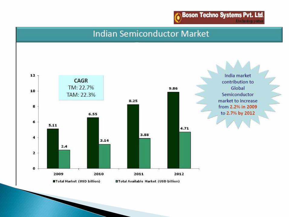
Semiconductor Manufacturing in India
The increasing spending on electronics products offers a large opportunity to global semiconductor
companies to set up their manufacturing plants in the country.
It is estimated that approximately seven to eight
Solar Photovoltaic (SPV) units will be set up in
India, with an investment of USD 5–6 billion.
The number of solar chip fab units in India is
expected to surpass the number of semiconductor
chip fab units in the country in the next few years.
Currently, there are no operational wafer
fabs in the country and the semiconductor
manufacturing is limited to only three
government companies (Bharat
Electronics Limited, Society for Integrated
Circuit Technology and Applied Research,
and Semi-Conductor Laboratory).
Semiconductor Manufacturing in India

India with the govt. support for setting up the lab firming up at about 40 percent of
the total cost , officials going ahead with the two big company – IBM and ST
Microelectronics . Typically , setting up a chip foundry cost around 4- 5 billion
USD .
India is trying to create an electronics manufacturing ecosystem to prevent the loss of
billions of dollars of foreign exchange in such imports every year . This bill, expected to
reach $SS billion (about Rs 3.4 lakh crore ) by 2020 from about $7 billion (Rs 43,600 crore ).
The centre has approved the setting up of two semiconductor wafer fabrication (FAB)
facilities in the country, involving total investment of Rs 63,410 crore.
These FAB units are to be set up by two consortia , one led by Jai Prakash Associate and other
led by HSMC Technologies India Pvt. Ltd. .
Jai Prakash Associates limited will partner IBM and Tower Jazz of Israel to invest.Rs34,399
crore . In a project to manufacture 90/65/45/28 nm chips, with an overall capacity of
40,000 WSPM. The project will be located along the Yamuna Expressway in Uttar Pradesh.
The project, to be located in Prantij, Gujarat, will have a capacity to manufacture 40,000
WSPM of 90/65/45/28/22 nm size.

12
Incentives under
National
Semiconductor
Policy
Assuming a 1:1 debt to equity
ratio for the project,
government restricts its
participation to 26 percent of
the equity capital.
There is also an option that
state governments can
provide additional incentives
to semiconductor companies.
In case of units located
outside the SEZ, the
Countervailing Duties
(CVD) on capital goods will
be exempted.
20 percent of the capital
expenditure of a
semiconductor manufacturing
unit located inside of Special
Economic Zone (SEZ) will be
carried by the government for
the first 10 years.
In case of units located
outside SEZ, government
will carry 25 percent of the
capital expenditure for the
stated time duration.
The policy covers LCDs,
storage devices, plasmas,
photo-voltaics, solar cells
and nanotechnology
products, and also includes
assembly and testing of
these products.
The threshold
investment for a
semiconductor
manufacturing (wafer
fabs) plant would be
approximately USD 575
million and for other
ancillary units (storage
devices, organic LED,
micro or nano-
technology products)
approximately USD 220
million.
These incentives are not extended
to older plants having second-
hand equipment.
Regulation of NSP
Incentives offered by the Government to the Companies
Regulatory Policy and Incentives Offered in
Semiconductor Sector

Sr. No Nano Technology Research Centre Place/Year of
Establishment
1 Bhabha Atomic Research Centre Mumbai ( 1954)
2 Center of Materials for Electronics
Technology
Pune ( 1990)
3 Central Electronics Research Institute Rajasthan (1953)
4. SSPL New Delhi (1962)
5 Saha Institute of Nuclear Physics Kolkata ( 1949)
6. S. N. Bose National Center for Basic
Sciences (DST)
Kolkata (1986)
7 National Physics Laboratories New Delhi
8 Defence Research and Development
Establishment (DRDE)
Gwalior (1973)
9 Regional Research Laboratories Trivandrum

10. Indian Association for the Cultivation of
Sciences (IACS)
Kolkata
11. Institute of Fundamental Research Mumbai
12. Central Scientific Instruments Organization Chandigarh
13 National Centre for Biological Sciences Karnataka
14 National Metallurgical Laboratory Jamshedpur
15 Raman Research Institute Bangalore
16 National Chemical Laboratories Pune
17 Central Glass and Ceramic Research Institute Kolkata


We are offering a business proposal to you in which we both can penetrate
Indian Semiconductor Market , which is full of lots of opportunities .
As I discussed Government of India promoting Investors to make their
products in India according to Make IN India scheme .
As we know your company has a brand name in manufacturing of Vacuum
coating equipments and process equipment like Sputtering , PECVD , CVD
etc.
We will make a marketing strategy for expansion of business and implement
those strategies with the help our skilled team in all over India .
Our team will bring enquiries by finding potential customer in all over india.
I believe , we both can create a land mark in semiconductor industry and this
will create history .

I would like to share that in India there are more than 500 educational institutes & universities , R&D center , Defense Institutes , which can be the target and new potential customers for the manual and small wire bonder equipments
Indian Government is injecting more money to modernize all above institutes , specially their NANOTECHNOLOGY and SEMICON departments therefore, we have been finding lots and lots of query from our these customers to enquire about manual and semi Automatic wire bonding equipments
As these are our existing customers for other range of products like plasma coating , PECVD and sputtering systems. Few customers are like
DMSRDE-Kanpur, Jamia Humdard University, Gurukul Kangri –Haridwar, IIT Ropar, S.N.Bose National Centre for Basic Sciences-Kolkata, JNCASR-Banglore and other DRDO and ISRO Labs.

We, Boson techno Systems, have our offices in 5 places across Indian and
enjoy the demographical advantage.
Right now we have 5 sales person and one service guy dedicated for the
wire bonder products, However as demand increases , we have willingness
and resources to add more head counts to cater to market and customers.
We normally share the manpower of our other division to tap the
semiconductor market, whenever the other division guy visit to any
customer, they share the complete product profile and share the lead with
SEMICON guys in case customer share interest for that.

Thanks !!!!!